Acer ACERPOWER M ACCURA User Manual

System Board
The M1A is a high-performance Pentium PCI-based system board
that supports the 64-bit Pentium microprocessor running at
75/90/100/120/133/ 150/166 MHz and has a 16-KB internal writ e-back
cache. It utilizes the Peripheral Component Inter connect (PCI) local
bus architecture. The PCI local bus maximizes the system
perform ance by enabling hi gh-speed peripherals to mat ch the speed
of the microprocessor with its 100/120/132 MB per second transfer
rate in burst mode.
The board has two memory banks composed of two 72-pin SIMM
sockets each that support a maximum system memory of 128 MB
using 32-MB SIMMs. The onboard 1-MB video memory is
upgradable to 2 MB for a higher vi deo r esol ution.
The system board f eatures a slot for the PCI/ ISA slot board and two
Mode 4 PCI enhanced IDE interfaces that support up to four IDE
devices. A 50- pin Fast SCSI-II i nterface with 10 MB/s transfer rate
come with t he system board to connect S CS I devices.
Standard I/O features such as two serial ports (COM1, COM2), one
parallel port, a di sket te drive inter face, and PS /2 mouse and keyboard
connectors reside on the system board.
System Board 1-1

1.1 Major Features
The system board has the following major features:
•
Pentium 75/90/ 100/120/ 133/150/ 166 MHz CPU i n an SP GA 296pin zero-insertion force (ZIF) socket
•
Two DRAM banks composed of f our 72-pin SIMM sockets that
support 4/8/16/32-MB 60/70ns SIMMs
•
16-KB internal cache (CPU)
•
256-KB synchronous or asynchronous second-level cache
•
128-KB Flash ROM for system BI OS and VGA BIOS
•
EISA-type connector f or the slot board t hat cont ains two PCI and
three ISA slots (for desktop housing) or three PCI and 5 ISA sl ots
(for minitower housing)
•
Two Enhanced IDE int er faces that support up to
four IDE devi c es
•
System clock/cal endar with 128/256 bytes CMOS RA M
•
External ports:
• PS/2 keyboard/ mouse ports
• Two buff er ed high-speed serial port s
• One ECP/EPP high-speed parall el port
• Video port
• RJ-45 Ethernet c onnec tor
1-2 User’s Guide

1.1.1 Layout
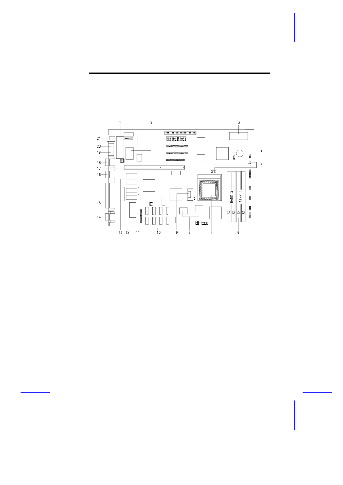
Figure 1-1 shows the locations of the system board major
components.
1 Keyboard controller
2 Real-time clock (RTC)
3 Flash ROM BIOS
4 Buzzer
5 Fan connectors
6 SIMM sockets
7 CPU socket
8 Synchronous cache (optional)
9 CPU voltage regulator
10 Asynchronous cache
11 VGA BIO S
1
12 Video upgrade sockets
13 Video RAM
14 Video port
15 Parallel port
16 COM 2
17 Slot board connector
18 COM 1
19 PS/2 mouse connector
20 PS/2 keyboard connector
21 RJ-45 connector
Figure 1-1 System Board Layout
1
For SCSI models onl y
System Board 1-3

1.1.2 Slot Board
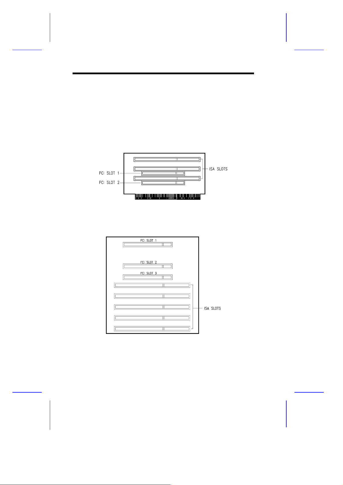
The system board com es with a slot board al ready i nstal l ed. The slot
board carries two PCI and three ISA bus slots for system
enhancements and future expansi on.
The slot board may v ar y i n size and l ayout depending on y our system
housing. Figur es 1-2 and 1-3 show the two kinds of slot boards.
Figure 1-2 2-PCI/3-ISA Slot Board (for desktop systems)
Figure 1-3 3-PCI/5-ISA Slot Board (for minitower systems)
1-4 User’s Guide

1.2 Jumpers and Connectors
1.2.1 Jumper and Connector Locations
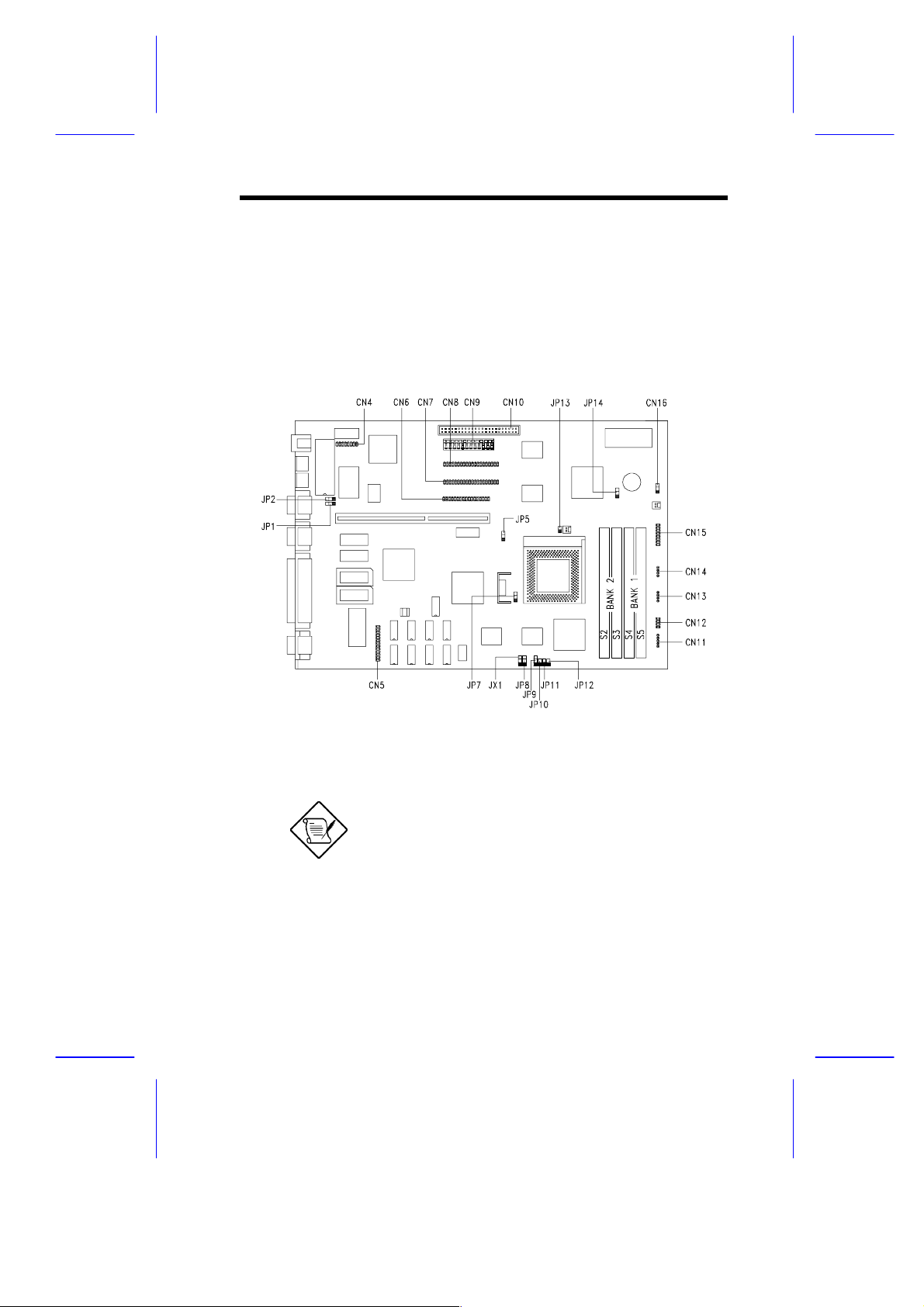
Figure 1-4 shows the jum per and connector l ocations on t he system
board.
Figure 1-4 System Board Jumper and Connector Locations
Jumpers are prefixed “JP”. Connectors are
prefixed “CN”.
The blackened pin of a jumper represents
pin 1.
System Board 1-5

1.2.2 Jumper Settings
Table 1-1 lists the system board jumpers with their corresponding
settings and func tions.
Table 1-1 System Board Jumper Settings
Jumper Setting Function
BIOS Type
JP1 1-2
2-3
Password Security
JP2 1-2
2-3
CPU Bus Frequency
JP5 Open
1-2
2-3
CPU Voltage
JP7 1-2
2-3
Reserved
JP9 2-3* Fixed setting. Do not reconfigure.
Reserved
JP14 Open* Leave open. Do not reconfigure.
For models with Acer BIOS
For models with OEM BIOS
Enable password
Disable password
50 MHz (Pentium 75 MHz)
60 MHz (Pentium 90/120/150 MHz)
66 MHz (Pentium 100/133/166
MHz)
VR (3.3V ± 5% - 0%)
VRE (3.45V ~ 3.6V)
1-6 User’s Guide
 Loading...