ZILOG Z8018933ASC, Z8018933FSC, Z8L18920ASC, Z8L18920FSC Datasheet

Zilog
FEATURES
PRELIMINARY
P
RELIMINARY PRODUCT SPECIFICATION
Z80189/Z8L189
GENERAL-PURPOSE
EMBEDDED CONTROLLERS
GENERAL-PURPOSE EMBEDDED CONTROLLERS
Z80189/Z8L189
Part CPU UART I/O Speed (MHz)
Z80189 S180* 16550 24 33
Z8L189 S180* 16550 24 20
■ Fully Static Z180™ MPU Core*
– On-Chip 1 MByte MMU
– Two Enhanced UART Channels (up to 512 Kbps)†
– Two Chain-Linked DMA Channels†
– x 2 Clock Multiplier
– Low-Power Consumption Modes
– Two 16-Bit Timer/Counters
– Clocked Serial I/O
– On-Chip Wait State Generator (WSG)
– On-Chip Interrupt Controller
On-Chip Clock Oscillator/Generator
–
■ 16550 Compatible MIMIC Interface
– 16 mA MIMIC Output Drive Capability
GENERAL DESCRIPTION
The Z80189/Z8L189 are cost-effective modem controllers
that address a new generation of data pumps having the
HDLC formatting feature. Data pumps of these types do
not require an HDLC interface; therefore, the Z80189 does
not need the ESCC™. The addition of the PC DMA Mailbox
Registers allow DMA data transfer between the PC memory
and the modem speaker/microphone CODEC. The Z80189
is a smart peripheral controller chip for modem (in particular V.34 applications), fax, voice messaging, and other
communications applications.
The Z80189/Z8L189 consists of an enhanced Z8S180
microprocessor, a 16550 MIMIC with increased MIMIC
drive capability for direct connection to the IBM PC, XT, AT
bus, and 24 bits of parallel I/O. Current PC modem software compatibility can be maintained with the Z80189's
ability to mimic the 16550 UART chip. The Z80180 core is
the intelligent controller between the data pump and
16550 MIMIC interface when used in internal applications.
This intelligent controller performs the data compression
and error correction on outgoing and incoming data.
■ Com Port Decode
■ PC DMA Mailbox Registers
■ Host I/O Mailbox
■ Programmable Fixed /ROMCS and
/RAMCS Boundaries
■ 100-Pin QFP and VQFP Packages
■ 3.3 and 5.0-Volt Operating Ranges
■ 0°C to +70°C Temperature Range
Notes:
† Enhancements from the Discrete S180 device.
The integration of COM Port Decode circuitry to the Z80189
allows the MIMIC to be selected for a specific COM Port
Address (PC COM Port Address 1-4). COM Port Decode
circuitry is simplified by allowing the user to select the
MIMIC COM Port addresses through software, in addition
to eliminating the need for external circuitry required for
COM Port Decode logic.
The PC DMA and I/O Mailbox Interface can be used to
provide communication paths between the PC Host and
the Z80189. These new communication paths can be used
for voice, DTAD, or jumperless COM Port selection.
Notes:
All Signals with a preceding front slash, "/", are active Low, e.g.:
B//W (WORD is active Low); /B/W (BYTE is active Low, only).
Power connections follow conventional descriptions below:
Connection Circuit Device
Power V
Ground GND V
CC
V
DD
SS
DS971890301
1
Zilog
PRELIMINARY
GENERAL DESCRIPTION (Continued)
GENERAL-PURPOSE EMBEDDED CONTROLLERS
Z80189/Z8L189
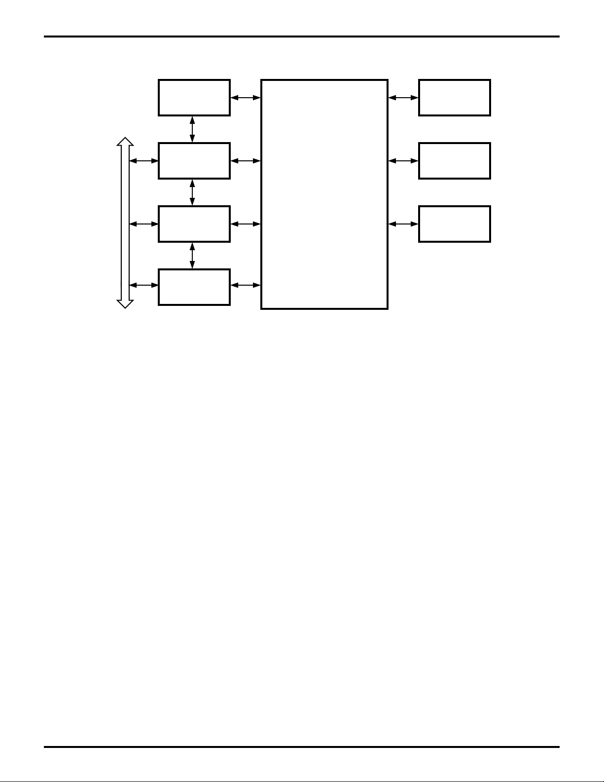
PC ISA BUS
Baud Rate
Generator
16550 MIMIC
Interface
COM Decoder
PC DMA
DMA & I/O
Interface
8-Bit Parallel
Port A
8-Bit Parallel
Port B
Enhanced
S180 MPU
8-Bit Parallel
Port C
Figure 1. Z80189 Block Diagram
2
DS971890301
Zilog
PIN DESCRIPTION
/NMI
/RESET
/HDACK1//BUSREQ
PRELIMINARY
PHI
VSS
/RD
/WR
/M1
/IOCS2/E
EXTAL
HA4//WAIT
XTAL
HDRQ1//BUSACK
/MRD//MREQ
/IORQ
HA3//RFSH
/HALT
/HCS/HC1
GENERAL-PURPOSE EMBEDDED CONTROLLERS
Z80189/Z8L189
HA2
HA1/RXA0
/INT0
/INT1/PC6
/INT2/PC7
ST
A0
A1
A2
A3
A4
A5
A6
A7
A8
A9
A10
A11
A12
VSS
A13
A14
A15
A16
A17
A18
VDD
A19
D0
D1
D2
D3
100
1
95
90
85
80
HA0
/HDDIS/TXA0
/HWR//CTS0
/HRD//DCD0
5
75
HINTR2
HAEN
HA6
VDD
HA7/IEI
10
70
/IOCS1/IEO
VSS
HA8
PC4
15
100-Pin QFP
65
Z80189/Z8L189
PC0
PC1
/MWR/PC2
PC3
PC5
HD7/PA7
20
60
HD6/PA6
HD5/PA5
HD4/PA4
HD3/PA3
HD2/PA2
25
55
HD1/PA1
HD0/PA0
EV2
EV1
30
50454035
/ROMCS
/RAMCS
DS971890301
D4
PB0/TXS
PB1//CTS0
PB4/RXA0
PB3/TXA0
PB2//DCD0
PB5/TXA1
PB6/RXA1
VSS
PB7/RXS//CTS1
/HDACK0/CKA0//DREQ0
HINTR1/TOUT
HA9/CKA1//TEND0
HC2/CKS
HA5//DREQ1
VDD
HDRQ0//RTS0
D7
D5
D6
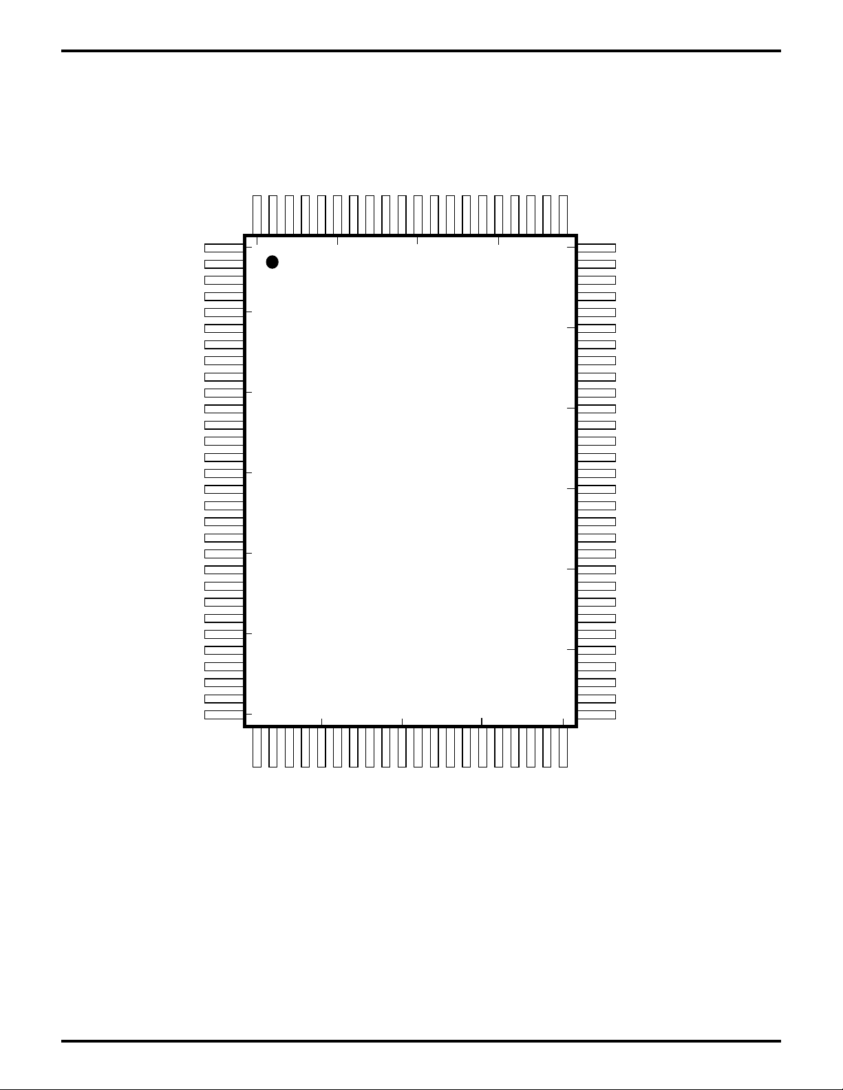
Figure 2. Z80189/Z8L189 100-Lead QFP Pin Identification
3
Zilog
PIN DESCRIPTION (Continued)
PRELIMINARY
GENERAL-PURPOSE EMBEDDED CONTROLLERS
Z80189/Z8L189
/HDDIS/TXA0
HA0
HA1/RXA0
HA2
/HCS/HC1
/HALT
HA3//RFSH
/IORQ
/MRD//MREQ
/IOCS2/E
/M1
/WR
/RD
PHI
VSS
XTAL
EXTAL
HA4//WAIT
HDRQ1//BUSACK
/HDACK1//BUSREQ
/RESET
/NMI
/INT0
/INT1/PC6
/INT2/PC7
/HRD//DCD0
/HWR//CTS0
75 51
76
80
85
90
95
100
125
HINTR2
HAEN
HA6
5
VDD
HA7/IEI
/IOCS/IEO
VSS
HA8
PC0
PC1
PC4
Z80189/Z8L189
100-Pin VQFP
10 15 20
/MWR/PC2
PC3
PC5
6070 5565
HD7/PA7
HD6/PA6
HD5/PA5
HD4/PA4
HD3/PA3
HD2/PA2
HD1/PA1
HD0/PA0
EV2
50
45
40
35
30
26
EV1
/ROMCS
/RAMCS
HDRQ0/RTS0
VDD
HA5//DREQ1
HC2/CKS
HINTR1/TOUT
HA9/CKA1//TEND0
VSS
/HDACK0/CKA0//DREQ0
PB7/RXS//CTS1
PB6/RXA1
PB5/TXA1
PB4/RXA0
PB3/TXA0
PB2//DCD0
PB1//CTS0
PB0/TXS
D7
D6
D5
D4
D3
D2
ST
A0A1A2
A3A4A5
A6A7A8
A9
A11
A10
A12
A14
A15
A16
A17
VSS
A13
A18
VDD
A19
D1
D0
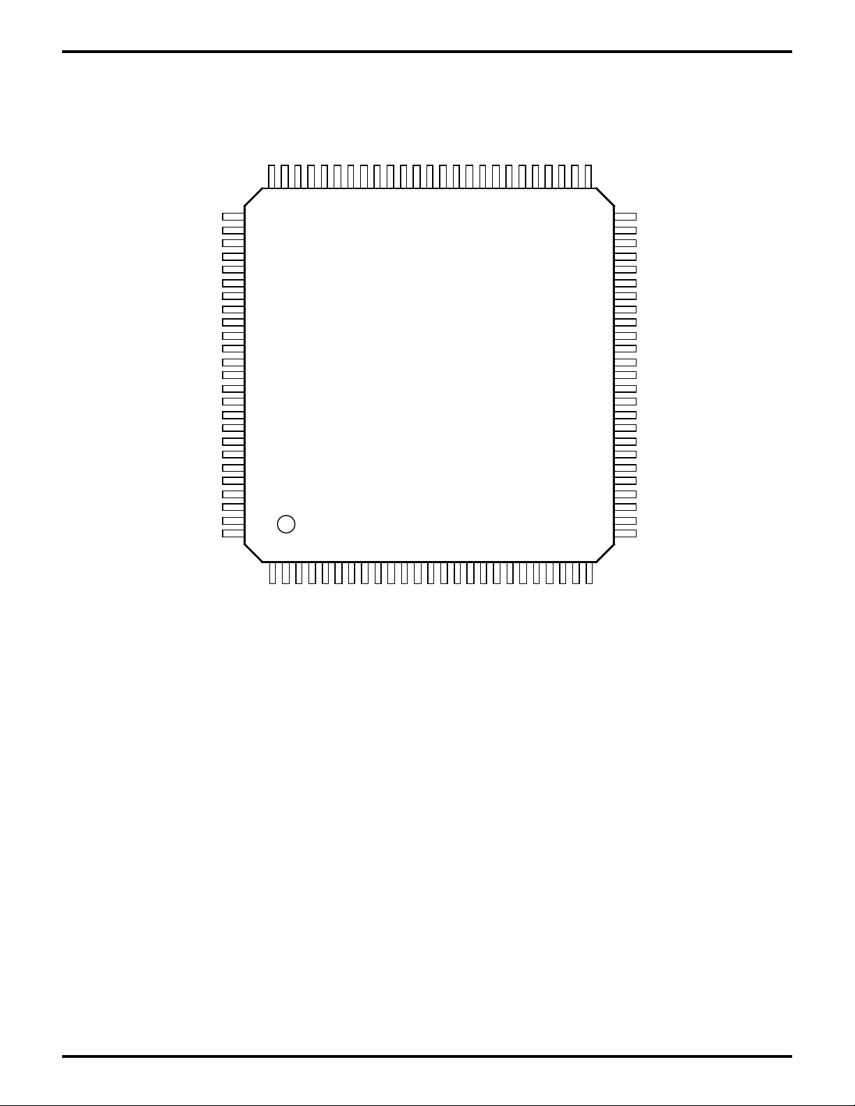
Figure 3. Z80189/Z8L189 100-Lead VQFP Pin Identification
4
DS971890301
Zilog
ABSOLUTE MAXIMUM RATINGS
PRELIMINARY
GENERAL-PURPOSE EMBEDDED CONTROLLERS
Z80189/Z8L189
Symbol Description Min Max Units
V
CC
V
IN
T
OPR
T
STG
Notes:
(*) Voltage on all pins with respect to GND.
Supply Voltage (*) –0.3 +7.0 V
Input Voltage –0.3 VCC+0.3 V
Operating Temp. 0 70 °C
Storage Temp. –55 +150 °C
STANDARD TEST CONDITIONS
The DC Characteristics and capacitance sections below
apply for the following standard test conditions, unless
otherwise noted. All voltages are referenced to GND (0V).
Positive current flows into the referenced pin (Test Load).
Available operating temperature range is:
S=0°C to 70°C
Voltage Supply Range:
+4.5V ≤ VCC ≤ +5.5V
+3.0V ≤ VCC ≤ +3.6V
Stresses greater than those listed under Absolute Maximum Ratings may cause permanent damage to the device. This is a stress rating only; operation of the device at
any condition above those indicated in the operational
sections of these specifications is not implied. Exposure to
absolute maximum rating conditions for extended periods
may affect device reliability.
= 2 mA
I
OL
1.4 V
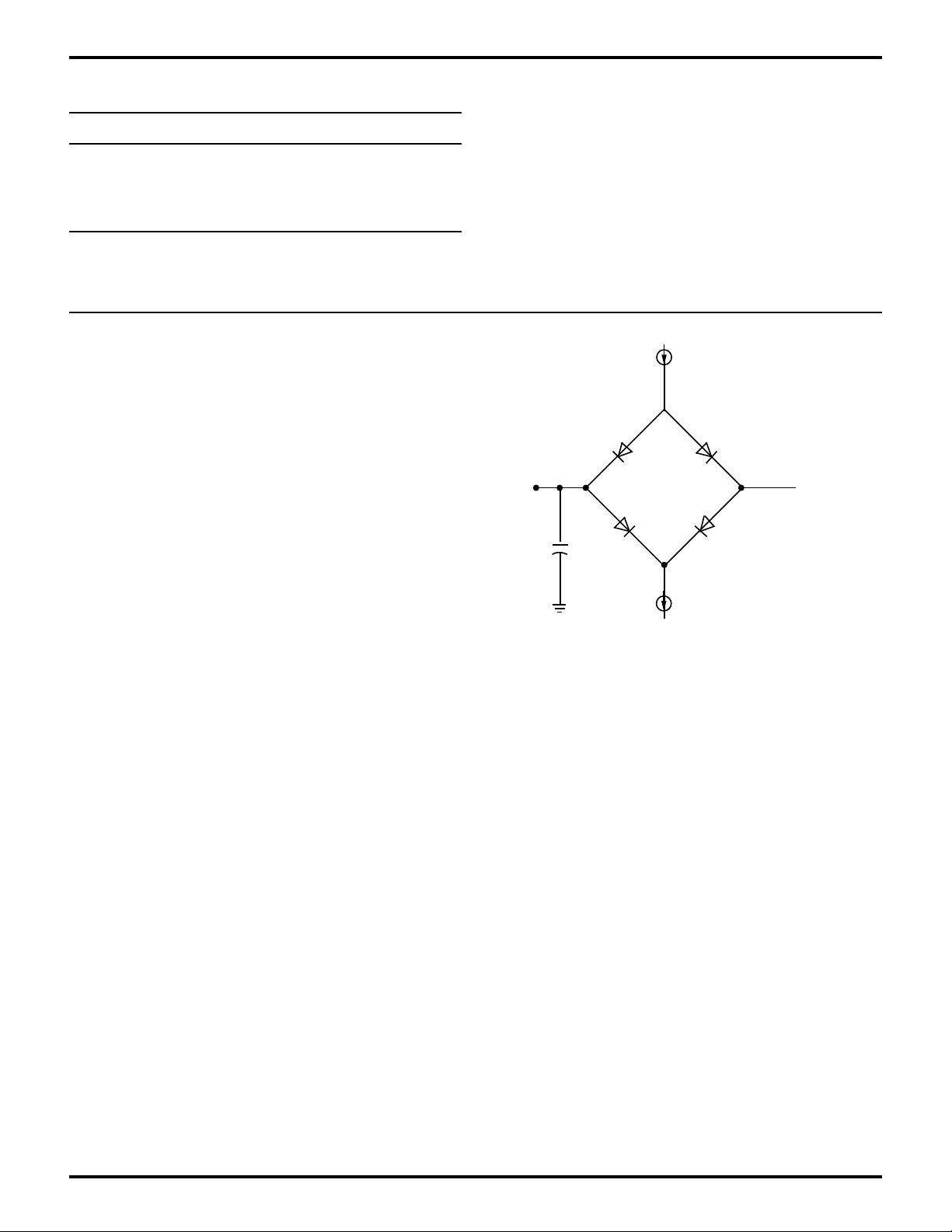
100 pF
All AC parameters assume a load capacitance of 50 pF.
Add 10 ns delay for each 50 pF increase in load up to a
maximum of 150 pF for the data bus and 100 pF for
address and control lines. AC timing measurements are
referenced to 1.5 volts (except for clock, which is referenced to the 10% and 90% points). Maximum capacitive
load for PHI is 125 pF.
= 250 µA
I
OH
Figure 4. Test Load Diagram
DS971890301
5

Zilog
PRELIMINARY
GENERAL-PURPOSE EMBEDDED CONTROLLERS
DC CHARACTERISTICS
Z80189
(V
= 5.0V ±10% or VCC = 3.3v ±10%, over specified temperature range unless otherwise noted.)
CC
Symbol Parameter Min Typ Max Unit Condition
Z80189/Z8L189
V
IH1
Input H Voltage VCC –0.6 VCC +0.3 V
RESET, EXTAL, NMI, INT0, INT1, INT2
V
IH2
Input H Voltage 2.0 VCC +0.3 V
Except RESET, EXTAL, NMI, INT0, INT1, INT2
V
IL1
Input L Voltage –0.3 0.6 V
RESET, EXTAL, NMI, INT0, INT1, INT2
V
IL2
Input L Voltage –0.3 0.8 V
Except RESET, EXTAL, NMI, INT0, INT1, INT2
V
OH1
Output H Voltage V
All outputs 2.4 V IOH = –200 µA
V
OH2
V
OL1
Output H PHI VCC –0.6 V I
= –200 µA
OH
Output L Voltage 0.40 V IOL = 2.2 mA
All outputs
V
OL2
V
OH
V
OL
V
OH
V
OL
I
IL
Output L PHI 0.40 V IOL= 2.2 mA
All MIMIC Outputs 2.4 V IOH = 16 mA,**
All MIMIC Outputs 0.4 V I
= 16 mA,**
OL
All MIMIC Outputs 2.4 V IOH =8 mA,VCC= 3.3 V**
All MIMIC Outputs 0.4 V I
=8 mA,VCC= 3.3 V**
OL
Input Leakage 10 µAVIN = 0 to VCC 5
Current All Inputs
Except XTAL, EXTAL
I
TL
Tri-State Leakage Current 10 µAVIN = 0 to VCC 5
ICC* Power Dissipation* 18 30 mA f = 20 MHz, 3.3v
Normal Operation 80 120 mA f = 33 MHz, 5v
ICC* Power Dissipation* 1.8 3.6 mA f = 20 MHz, 3.3v
(System STOP Mode) 6 9 mA f = 33 MHz, 5v
Power Dissipation 15 50 µA
(Standby Mode)
Notes:
* VIH Min = VCC -1.0 V, V
** Total loading current in or out of the Z189 cannot exceed 150 mA from
pins 41 to 70.
Max = 0.8 V (all output terminals are at no load).
IL
6
DS971890301
Zilog
TIMING DIAGRAMS
PRELIMINARY
GENERAL-PURPOSE EMBEDDED CONTROLLERS
Z80189/Z8L189
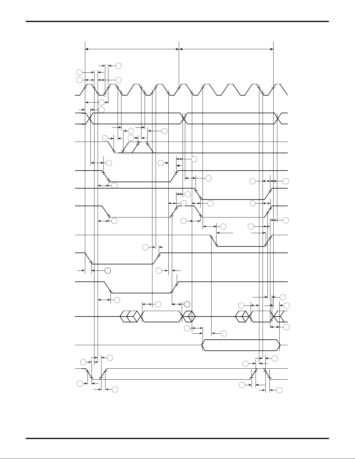
ø
Address
/WAIT
/MREQ
/IORQ
/RD
/WR
Opcode Fetch Cycle
I/O Write Cycle †
I/O Read Cycle †
T1 T2 TW T3 T1 T2 TW T3 T1
5
4
32
1
6
19
20
19
7
8
9
14
12
20
11
7
11
13 28
9
22
13
25
26 and 26a
1129
11
/M1
ST
Data
IN
Data
OUT
/RESET
68
62
10
17
63
67
15
18
23
16
15
24
62
67
Figure 5. CPU Timing
(Opcode Fetch Cycle, Memory Read/Write Cycle I/O Read/Write Cycle)
16
21
27
63
68
DS971890301
7
Zilog
TIMING DIAGRAMS (Continued)
Ø
32
31
/INTI
33
/NMI
/INTSCC
/M1 [1]
PRELIMINARY
C7
30
GENERAL-PURPOSE EMBEDDED CONTROLLERS
Z80189/Z8L189
/IORQ [1]
/Data IN [1]
/MREQ [2]
/RFSH [2]
/BUSREQ
/BUSACK
Address
Data /MREQ,
/RD, /WR,
/IORQ
16
15
39
4041 42
35 35
34
43
[3]
34
3736
3838
44
/HALT
Notes:
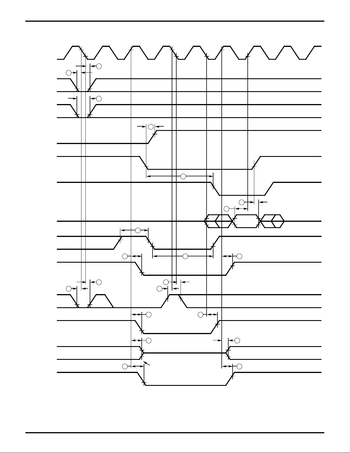
[1] During /INT0 acknowledge cycle
[2] During refresh cycle
[3] Output buffer is off at this point
Figure 6. CPU Timing
(/INT0 Acknowledge Cycle, Refresh Cycle, BUS RELEASE Mode
HALT Mode, SLEEP Mode, SYSTEM STOP Mode)
8
DS971890301
Zilog
TIMING DIAGRAMS (Continued)
PRELIMINARY
GENERAL-PURPOSE EMBEDDED CONTROLLERS
Z80189/Z8L189
Address
/IROQ
/RD
/WR
I/O Read Cycle
T1 T2 TW T3 T1
0
28
9
CPU or DMA Read/Write Cycle (Only DMA Write Cycle for /TENDi)
T1 T2 Tw T3 T1
29
13
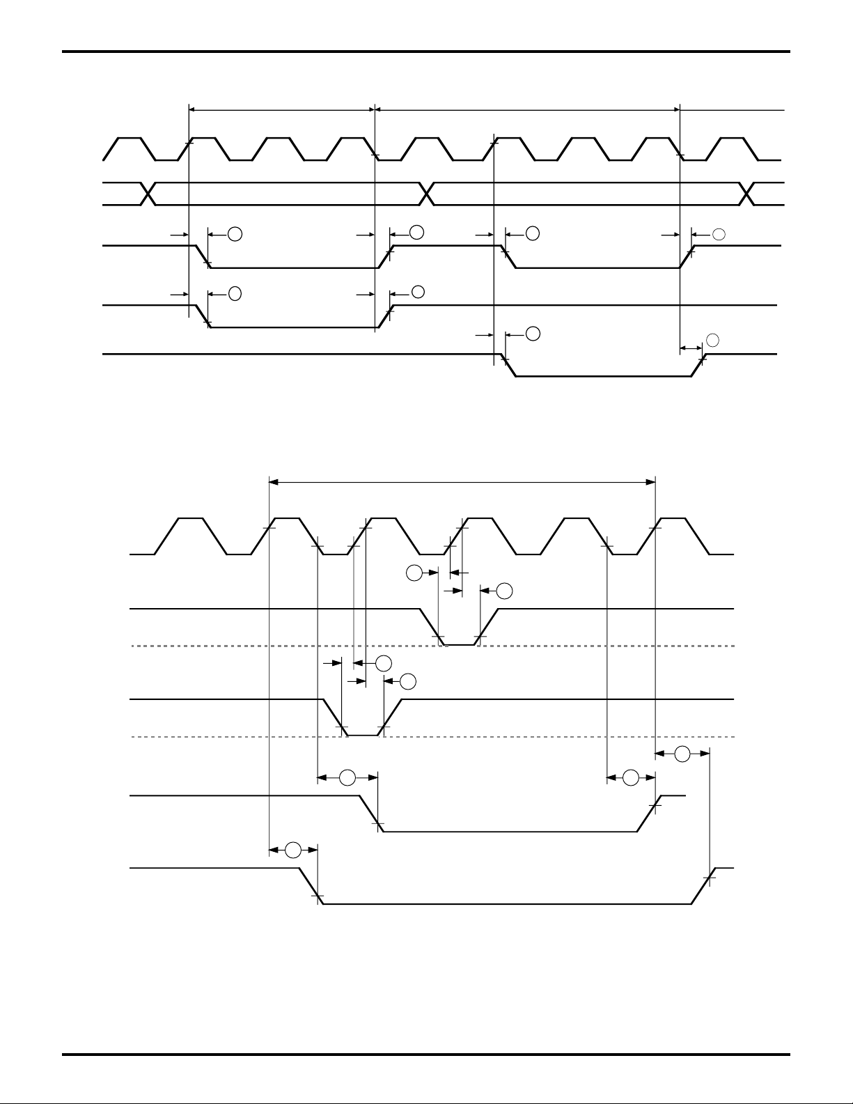
Figure 7. CPU Timing
I/O Write Cycle
T2 TW T3
28
22
29
25
/DREQi
(At level
sense)
/DREQi
(At edge
sence)
/TENDi
ST
Ø
45
[1]
46
45
[2]
45
18
47
48
[4]
[3]
17
DMA Control Signals
[
1] tDRQS and tDRQH are specified for the rising edge of clock followed by T3.
[2] tDRQS and tDRQH are specified for the rising edge of clock.
[3] DMA cycle starts.
[4] CPU cycle starts.
DS971890301
Figure 8. DMA Control Signals
9
Zilog
TIMING DIAGRAMS (Continued)
T1 T2 Tw Tw T3
Ø
PRELIMINARY
49 50
49 50
49 50
GENERAL-PURPOSE EMBEDDED CONTROLLERS
Z80189/Z8L189
1615
D7-D0
Ø
BUS RELEASE Mode
E
SLEEP Mode
SYSTEM STOP Mode
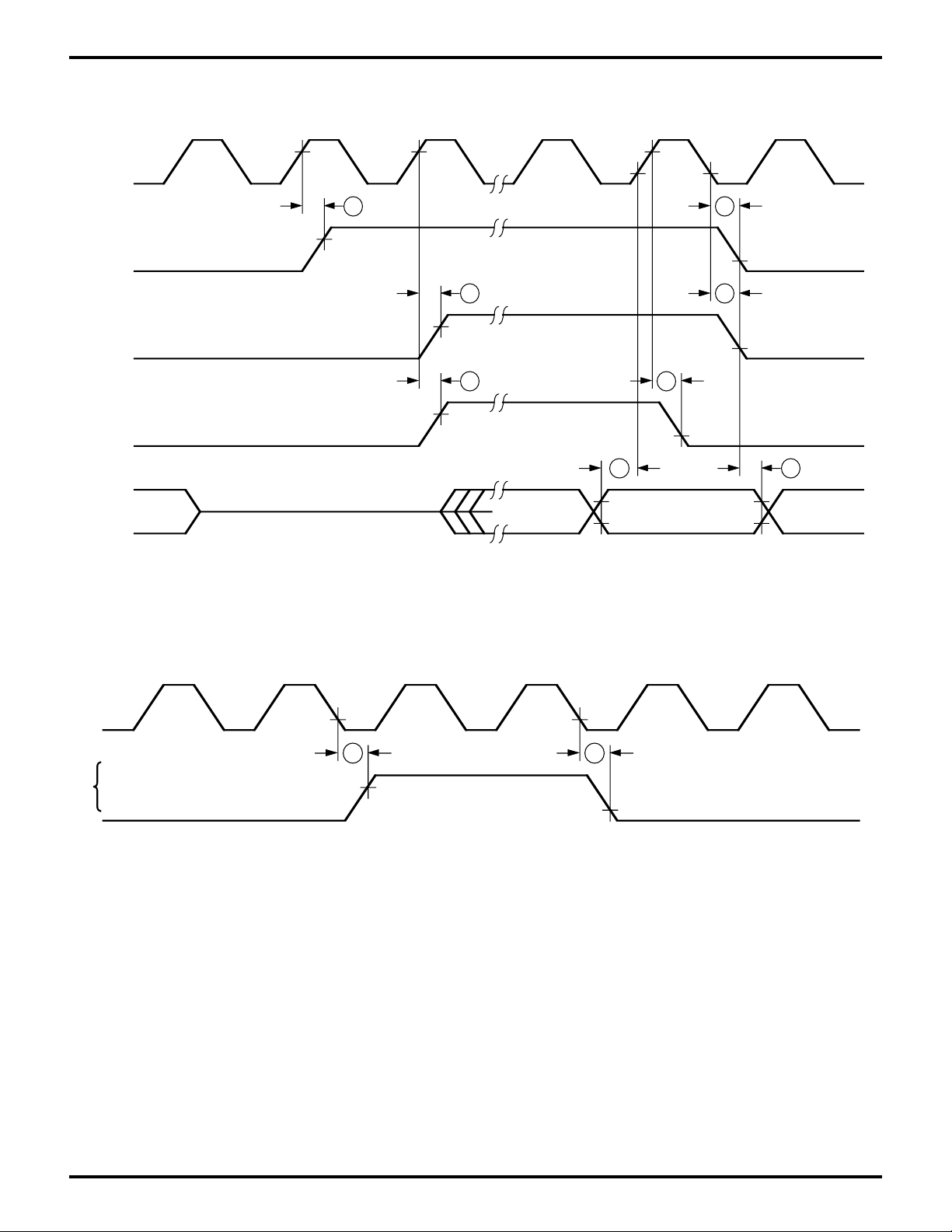
Figure 9. E Clock Timing
(Memory Read/Write Cycle
I/O Read/Write Cycle)
5049
Figure 10. E Clock Timing
10
DS971890301
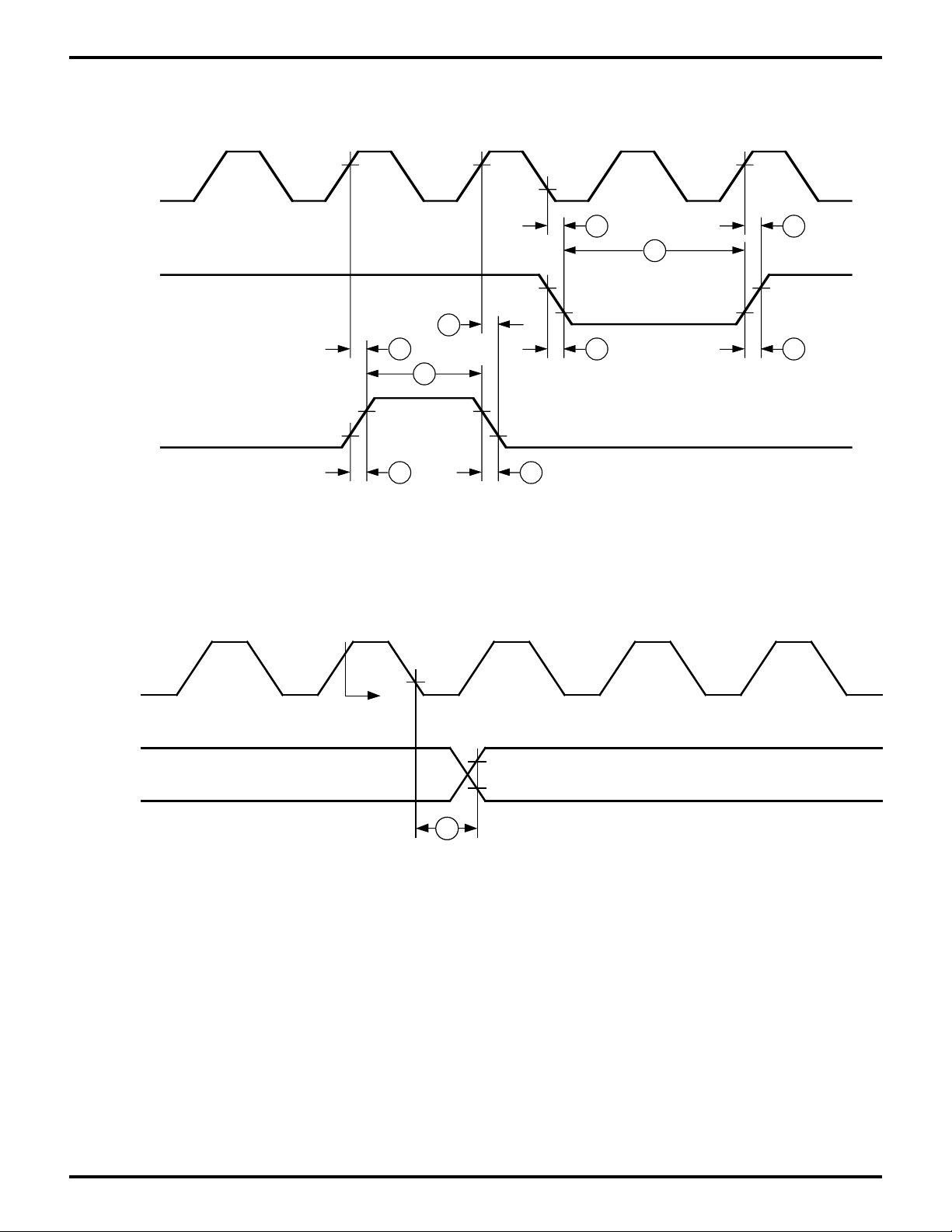
Zilog
TIMING DIAGRAMS (Continued)
T2 Tw T3 T1 T2
Ø
PRELIMINARY
GENERAL-PURPOSE EMBEDDED CONTROLLERS
Z80189/Z8L189
(Example:
I/O Read -
Opcode
Fetch)
(I/O Write)
Ø
50
52
49
E
50
49
51
54
53
E
53
54
Figure 11. E Clock Timing
(Minimum timing example
of PWEL and PWEH)
TOUT
Timer Data
Reg = 0000H
55
Figure 12. Timer Output Timing
DS971890301
11
Zilog
TIMING DIAGRAMS (Continued)
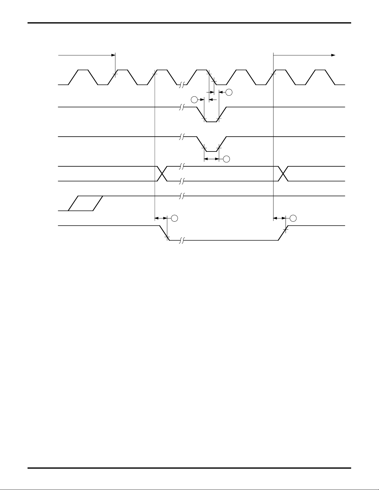
SLP Instruction Fetch Next Opcode Fetch
T3 T1 T2 TS TS T1 T2
Ø
/INTi
/NMI
A18-A0
PRELIMINARY
32
31
33
GENERAL-PURPOSE EMBEDDED CONTROLLERS
Z80189/Z8L189
/MREQ, /M1
/RD
/HALT
43 44
Figure 13. SLEEP Execution Cycle
12
DS971890301
Zilog
TIMING DIAGRAMS (Continued)
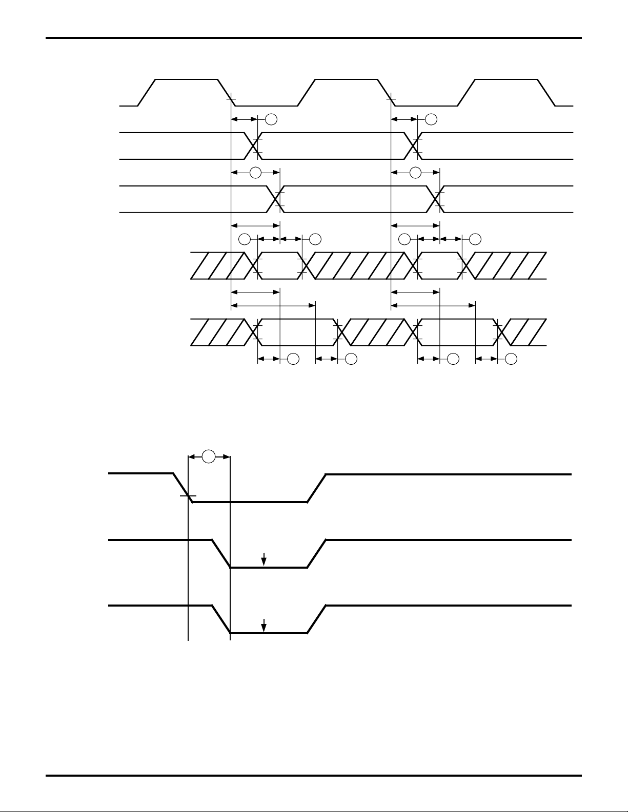
CSI/O Clock
Transmit Data
(Internal Clock)
Transmit Data
(External Clock)
Receive Data
(Internal Clock)
PRELIMINARY
56 56
5757
11 tcyc 11 tcyc
5958 5958
GENERAL-PURPOSE EMBEDDED CONTROLLERS
Z80189/Z8L189
Receive Data
(External Clock)
/MREQ
/RAMCS
11.5 tcyc
16.5 tcyc 16.5 tcyc
6160 60 61
Figure 14. CSI/O Receive/Transmit Timing
71
11.5 tcyc
/ROMCS
DS971890301
Figure 15. /ROMCS and /RAMCS Timing
13
Zilog
TIMING DIAGRAMS (Continued)
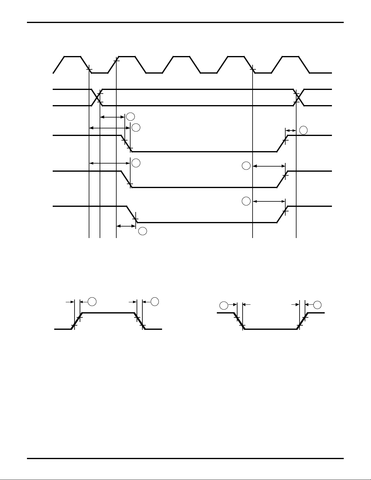
T1 T2 TW T3 T1
0
PRELIMINARY
GENERAL-PURPOSE EMBEDDED CONTROLLERS
Z80189/Z8L189
Address
/MREQ
/RD
/WR
Address Valid
7
8
9
22
Figure 16. /MWR and /MRD Timing
11
13
24
65 66
EXTAL
VIL1
Figure 17. External Clock Rise Time and Fall Time
14
VIH1
VIH1
VIL1
70
Figure 18. Input Rise and Fall Time
(Except EXTAL, /RESET)
DS971890301
69

Zilog
PRELIMINARY
GENERAL-PURPOSE EMBEDDED CONTROLLERS
Z80189/Z8L189
AC CHARACTERISTICS
(V
= 5V ±10% or VCC = 3.3V ±10%, over specified temperature range unless otherwise noted
CC
33 MHz Characteristics Apply Only to 5V Operation.)
Z8L189-20 MHz Z80189-33 MHz
No Sym Parameter Min Max Min Max Unit Notes
1 tcyc Clock Cycle Time 50 2000 33 2000 ns [1]
2 tCHW Clock H Pulse Width 15 10 ns [1]
3 tCLW Clock L Pulse Width 15 10 ns [1]
4 tcf Clock Fall Time 10 5 ns [1]
5 tcr Clock Rise Time 10 5 ns [1]
6 tAD /PHI to Address Valid 15 15 ns
7 tAS Address Valid to /MREQ, /IRQ 5 5 ns
8 tMED1 /PHI to /MREQ Delay 3 3 ns [3]
9 tRDD1 /PHI to /RD Delay (IOC=1) 25 15 ns
/ PHI to /RD Delay (IOC=0) 25 15 ns
10 tM1D1 /PHI to /M1 Delay 35 15 ns
11 tAH Address Hold Time from (MREQ, IOREQ, RD, WR) 5 5 ns
12 tMED2 /PHI to /MREQ Delay 25 15 ns
13 tRDD2 /PHI to /RD Delay 25 15 ns
14 tM1D2 /PHI to /M1 Delay 40 15 ns
15 tDRS Data Read Setup Time 10 10 ns [3]
16 tDRH Data Read Hold Time 0 0 ns
17 tSTD1 /PHI to /ST Delay 30 15 ns
18 tSTD2 /PHI to /ST Delay 30 15 ns
19 tWS WAIT Setup Time to /PHI 15 10 ns [2]
20 tWH WAIT Hold Time from /PHI 10 5 ns
21 tWDZ /PHI to Data Float Display 35 20 ns
22 tWRD1 /PHI to /WR Delay 25 15 ns
23 tWDD /PHI to Write Data Delay Time 25 15 ns
24 tWDS Write Data Setup Time to /WR 10 10 ns
25 tWRD2 /PHI to /WR Delay 25 15 ns
26 tWRP Write Pulse Width (Memory Write Cycle) 75 45 ns
26a tWRP Write Pulse Width (I/O Write Cycle) 130 70 ns
27 tWDH Write Data Hold Time from /WR 10 5 ns
28 tIOD /PHI to /IORQ Delay (IOC=1) 25 15 ns
/PHI to /IORQ Delay (IOC=0) 25 15 ns
29 tIOD2 /PHI to /IORQ Delay 25 15 ns
30 tIOD3 /M1 to /IORQ Delay 100 80 ns
31 tINTS /INT Setup Time to /PHI 20 15 ns
32 tINTH /INT Hold Time from /PHI 10 10 ns
33 tNMIW NMI Pulse Width 35 25 ns
34 tBRS BUSREQ Setup Time to /PHI 10 10 ns
35 tBRH BUSREQ Hold Time from /PHI 10 10 ns
36 tBAD1 /PHI to /BUSACK Delay 25 15 ns
37 tBAD2 /PHI to /BUSACK Delay 25 15 ns
38 tBZD /PHI to Bus Floating Delay Time 40 30 ns
39 tMEWH MREQ Pulse Width (High) 35 25 ns
40 tMEWL MREQ Pulse Width (Low) 35 25 ns
DS971890301
15

Zilog
PRELIMINARY
GENERAL-PURPOSE EMBEDDED CONTROLLERS
AC CHARACTERISTICS (Continued)
Z80189/Z8L189
(V
= 5V ±10% or VCC = 3.3V ±10%, over specified temperature range unless otherwise noted
CC
33 MHz Characteristics Apply Only to 5V Operation.)
Z8L189-20 MHz Z80189-33 MHz
No Sym Parameter Min Max Min Max Unit Notes
41 tRFD1 /PHI to /RFSH Delay 20 15 ns
42 tRFD2 /PHI to /RFSH Delay 20 15 ns
43 tHAD1 /PHI to /HALT Delay 15 15 ns
44 tHAD2 /PHI to /HALT Delay 15 15 ns
45 tDRQS DREQ Setup Time to /PHI 20 15 ns
46 tDRQH DREQ Hold Time from /PHI 20 15 ns
47 tTED1 /PHI to /TEND Delay 25 15 ns
48 tTED2 /PHI to /TEND Delay 25 15 ns
49 tED1 /PHI to /E Delay 30 15 ns
50 tED2 /PHI /or to /E Delay 30 15 ns
51 PWEH E Pulse Width (High) 25 20 ns
52 PWEL E Pulse Width (Low) 50 40 ns
53 tEr Enable Rise Time 10 10 ns
54 tEf Enable Fall Time 10 10 ns
55 tTOD /PHI to Timer Output Delay 75 50 ns
56 tSTDI CSI/O Transmit Data Delay (Internal Clock Operation) 75 60 ns
57 tSTDE CSI/O Transmit Data Delay (External Clock Operation) 7.5 tcyc+75 7.5 tcyc+60 ns
58 tSRSI CSI/O Receive Data Setup Time (Internal Clock Operation) 1 1 phi cycles
59 tSRHI CSI/O Receive Data Hold Time (Internal Clock Operation) 1 1 phi cycles
60 tSRSE CSI/O Receive Data Setup Time (External Clock Operation) 1 1 phi cycles
61 tSRHE CSI/O Receive Data Hold Time (External Clock Operation) 1 1 phi cycles
62 tRES RESET Setup Time to /PHI 40 25 ns
63 tREH RESET Hold Time from /PHI 25 15 ns
64 tOSC Oscillator Stabilization Time 20 20 ns
65 tEXr External Clock Rise Time (EXTAL) 10 5 ns
66 tEXf External Clock Fall Time (EXTAL) 10 5 ns
67 tRr Reset Rise Time 50 50 ms [2]
68 tRf Reset Fall Time 50 50 ms [2]
69 tIr Input Rise Time (Except EXTAL, RESET) 50 50 ns [2]
70 tIf Input Fall Time (Except EXTAL, RESET) 50 50 ns [2]
71 tdCS MREQ Valid to RAMCS and ROMCS Valid Delay 5 5 ns [3]
Notes:
[1] tcyc = tCHW + tCLW + tcf + tcr.
[2] If the rise and fall times are greater than the specified maximums,
other specifications will not be met.
[3] SL1832 is test screened such that specifications 8, 15, and 71 are
tested to 18 ns (Tmeol + Tors + Trlcs = 18 ns).
16
DS971890301
Zilog
PRELIMINARY
AC CHARACTERISTICS (Continued)
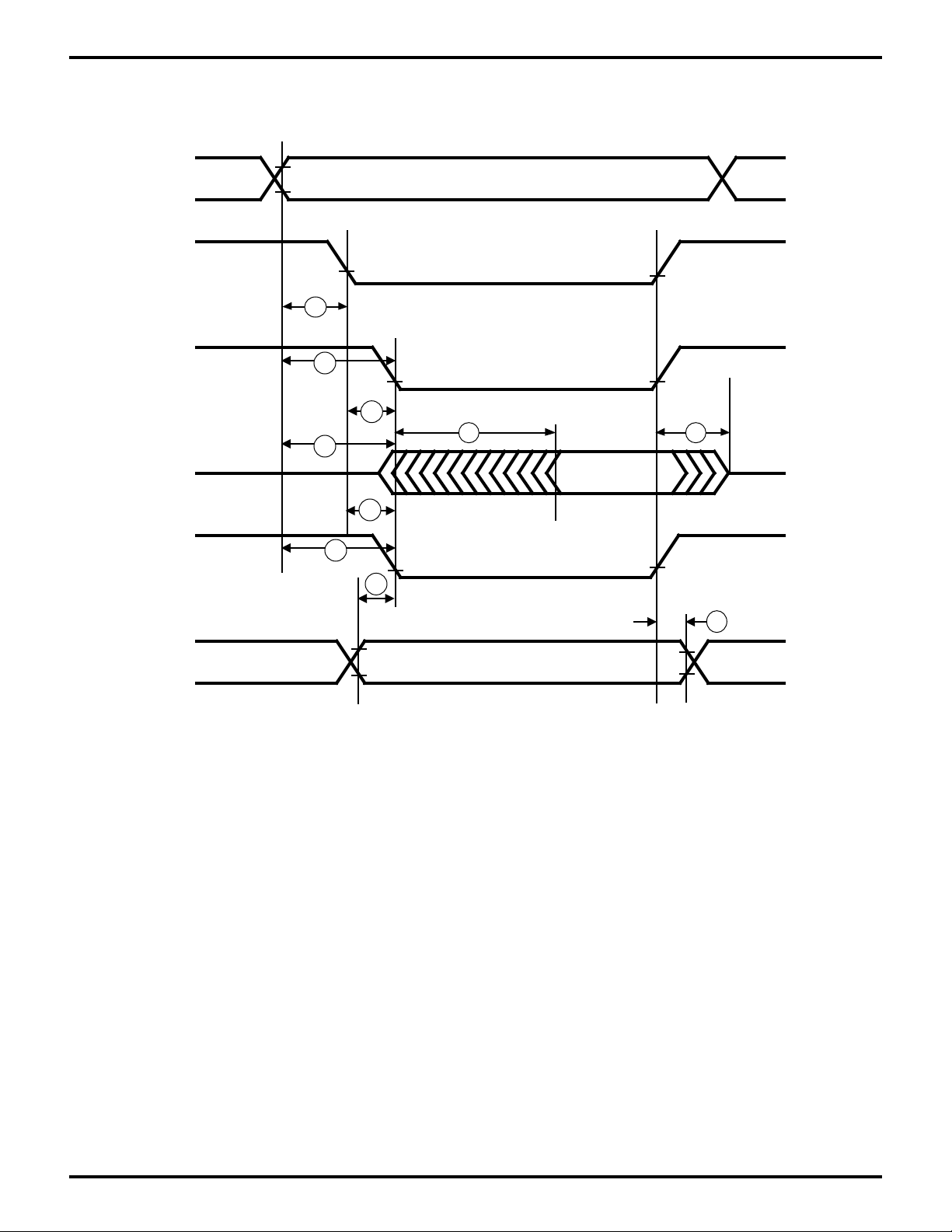
Read/Write External Bus Master Timing
GENERAL-PURPOSE EMBEDDED CONTROLLERS
Z80189/Z8L189
Address
/IORQ
/RD
Data
/WR
A7-A0
7
8
2
1
4
5
Data Out
2
9
6
3
Data
Data In
Figure 19. Read/Write External Bus Master Timing
DS971890301
17

Zilog
PRELIMINARY
GENERAL-PURPOSE EMBEDDED CONTROLLERS
Z80189/Z8L189
AC CHARACTERISTICS (Continued)
Read/Write External Bus Master Timing
Table 1. External Bus Master Timing
Z8L189-20 MHz Z80189-33 MHz
No Sym Parameter Min Max Min Max Unit Notes
1 TsA(wf)(rf) Address to WR or RD Fall Time 20 20 ns
2 TsIO(wf)(rf) IORQ Fall to WR or RD Fall Time 20 20 ns
3 Th Data Hold Time (from WR Rise) 0 0 ns
4 TdRD(DO) RD Fall to Data Out Delay 35 35 ns
5 TdRIr(DOz) RD, IORQ Rise to Data Float Time 0 0 ns
6 TsDI(WRf) Data In to WR Fall Setup Time 20 20 ns
7 TsA(IORQf) Address to IORQ Fall Setup Time 35 35 ns
8 TsA(RDf) Address to RD Fall Setup Time 35 35 ns
9 TsA(WRf) Address to WR Fall Setup Time 35 35 ns
Table 2. 16550 MIMIC Timing
Z8L189-20 MHz Z80189-33 MHz
No Sym Parameter Min Max Min Max Unit Notes
1 TsAR Address Setup to HRD Fall Time 30 30 ns
2 TsCSR Address Setup to CS Fall Time 30 30 ns
3 TsAW Address Setup to HWR Fall Time 30 30 ns
4 TsCSW HCS Setup to HWR Fall Time 30 30 ns
5 tAh Address Hold Time 20 20 ns
6 tCSh HCS Hold Time 20 20 ns
7 tDs Data Setup Time 30 30 ns
8 tDh Data Hold Time 30 30 ns
9 tWc Write Cycle Delay 2.5 2.5 phi cycles
10 tRvD Delay from HRD Fall to Data Valid 125 125 ns
11 tHz HRD Rise to Data Float Delay 100 100 ns
12 tRc Read Cycle Delay 125 125 ns
13 tRDD HRD Toggle to Driver Enable/Disable 60 60 ns
14 tSINT Delay fromwr RBR Reg. to Assert HINTR 2.0 2.0 phi cycles
15 tRINT Delay from /HRD of RBR to Deassert HINTR 2.0 2.0 phi cycles
16 tHR Delay from /WR THR to Reset HINTR 2.5 2.5 phi cycles
17 TSTI Delay from MPU /RD of THR to Assert HINTR 2.0 2.0 phi cycles
18 TIR Delay from /RD to Reset Interrupt 75 75 ns
18
DS971890301
Zilog
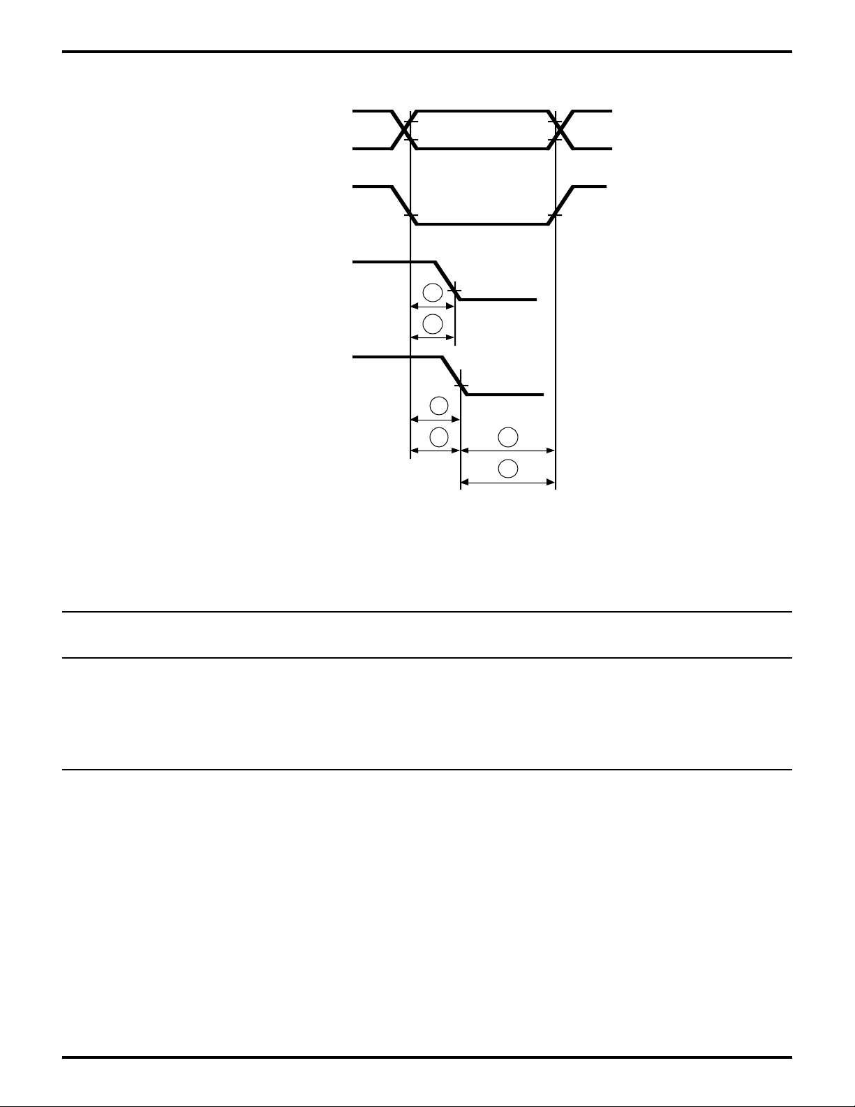
16550 MIMIC TIMING
/HCS
PRELIMINARY
ValidHA2, HA1, HA0
GENERAL-PURPOSE EMBEDDED CONTROLLERS
Z80189/Z8L189
/HRD
/HWR
Figure 20. PC Host /RD /WR Timing
Table 3. PC Host /RD /WR Timing Table
No Symbol Parameter Min Max Min Max Units
1 TsAR H Address to/HRD Fall Setup 30 30 ns
2 tsCSR /HCS to /HRD Fall Setup 30 30 ns
3 tsAW H Address to /HWR Fall Setup 30 30 ns
4 tsCSW /HCS to /HRD Fall Setup 30 30 ns
5 tAh H Address from /HRD /HWR Hold 20 20 ns
6 tCSh /HCS from /HRD /HWR Hold 20 20 ns
1
2
3
4 5
6
Z80L189-20 MHz Z80189-33 MHz
DS971890301
19
Zilog
16550 MIMIC TIMING (Continued)
HAEN
PRELIMINARY
Valid/HA3 - /HA9
GENERAL-PURPOSE EMBEDDED CONTROLLERS
Z80189/Z8L189
/HRD
/HWR
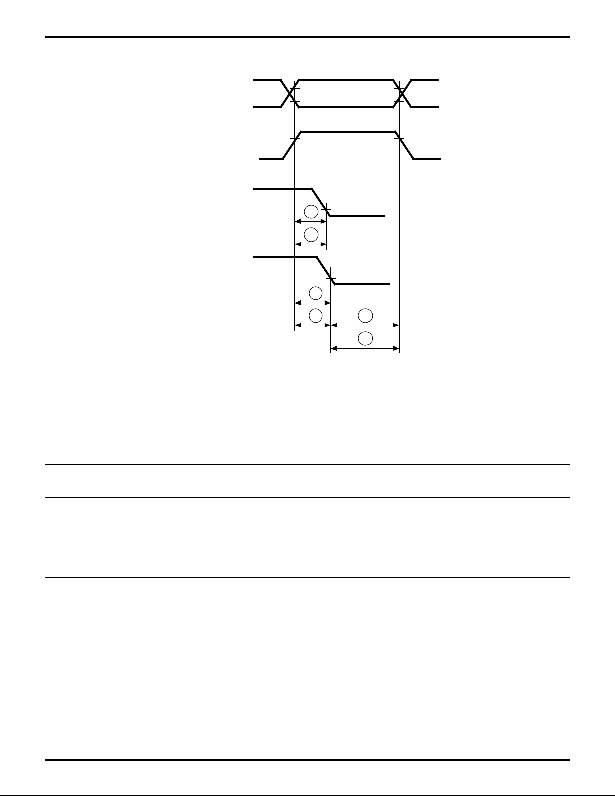
Figure 21. Com Port Decode Mode
PC Host /RD /WR Timing
Table 4. Com Port Decode Mode
PC Host /RD /WR Timing Table
No Symbol Parameter Min Max Min Max Units
1
2
3
4 5
6
Z8L189-20 MHz Z80189-33 MHz
1 tsAR H Address to/HRD Fall Setup 30 30 ns
2 tsCSR /HCS to /HRD Fall Setup 30 30 ns
3 tsAW H Address to /HWR Fall Setup 30 30 ns
4 tsCSW /HCS to /HRD Fall Setup 30 30 ns
5 tAh H Address from /HRD /HWR Hold 20 20 ns
6 tCSh /HCS from /HRD /HWR Hold 20 20 ns
20
DS971890301
Zilog
16550 MIMIC TIMING (Continued)
/HWR
PRELIMINARY
ValidHD7-HD0
GENERAL-PURPOSE EMBEDDED CONTROLLERS
Z80189/Z8L189
7
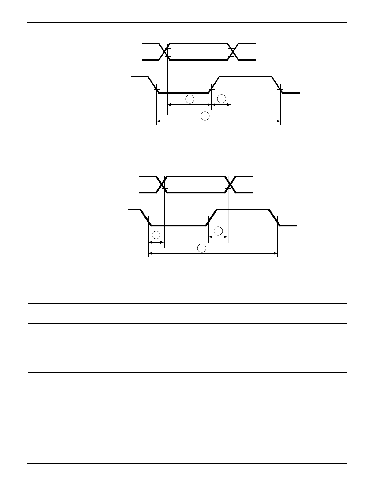
Figure 22. Data Setup and Hold, Output Delay, Write Cycle
ValidHD7-HD0
/HRD
10
12
Figure 23. Data Setup and Hold, Output Delay, Read Cycle
8
9
11
Table 5. Data Setup and Hold, Output Delay, Read Cycle Table
Z8L189-20 MHz Z80189-33 MHz
No Sym Parameter Min Max Min Max Units
7 tDs Data In to /HWR Rise Setup 30 30 ns
8 tDh Data In from /HWR Rise Hold 30 30 ns
9 tWc Write Cycle Delay 2.5 2.5 phi cycles
10 tRvd /HRD Fall to Data Out Valid Delay 125 125 ns
11 THz /HRD Rise to Data Out Float Delay 100 100 ns
12 tRc Read Cycle Delay 2.5 2.5 phi cycles
DS971890301
21
Zilog
PRELIMINARY
GENERAL-PURPOSE EMBEDDED CONTROLLERS
16550 MIMIC TIMING (Continued)
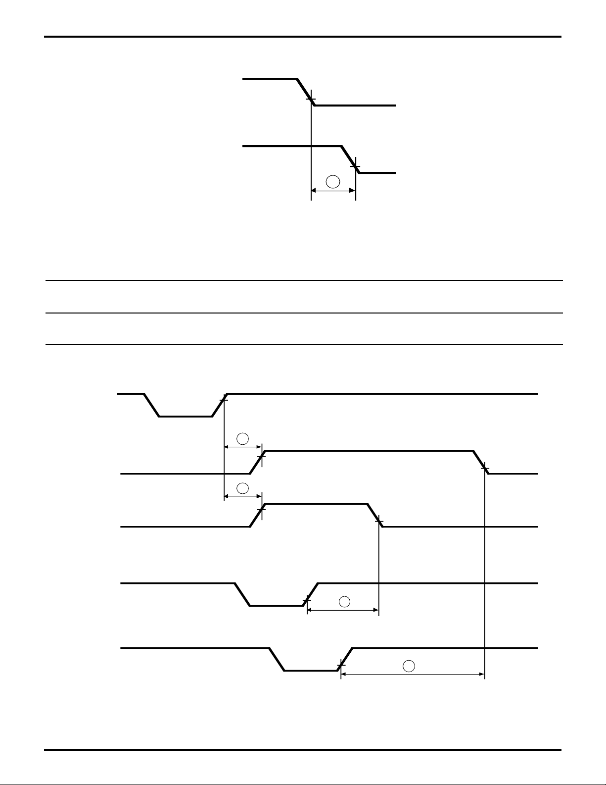
/HRD
/HDDIS
13
Figure 24. Driver Enable Timing
Table 6. Driver Enable Timing Table
Z8L189-20 MHz Z80189-33 MHz
No Sym Parameter Min Max Min Max Units
Z80189/Z8L189
13 tRDD /HRD to Driver
Enable/Disable 60 60 ns
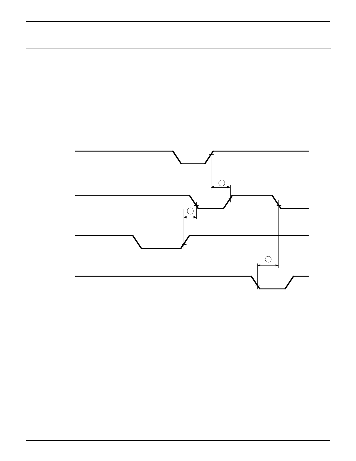
/WR (MPU)
RBR
HINTR
(Trigger
Level)
HINTR
(Line
Status
RDR
/HRD LSR
14
14
15
22
/HRD RBR
15
Figure 25. Interrupt Timing RCVR FIFO
DS971890301
Zilog
PRELIMINARY
GENERAL-PURPOSE EMBEDDED CONTROLLERS
16550 MIMIC TIMING (Continued)
Table 7. Interrupt Timing RCVR FIFO Table
Z8L189-20 MHz Z80189-33 MHz Units
No Sym Parameter Min Max Min Max
14 tSINT Delay from Stop to Set 2 2 phi cycles
Interrupt
15 tRINT Delay from /HRD
(RD RBR or RD LSR) 2 2 phi cycles
to Reset Interrupt
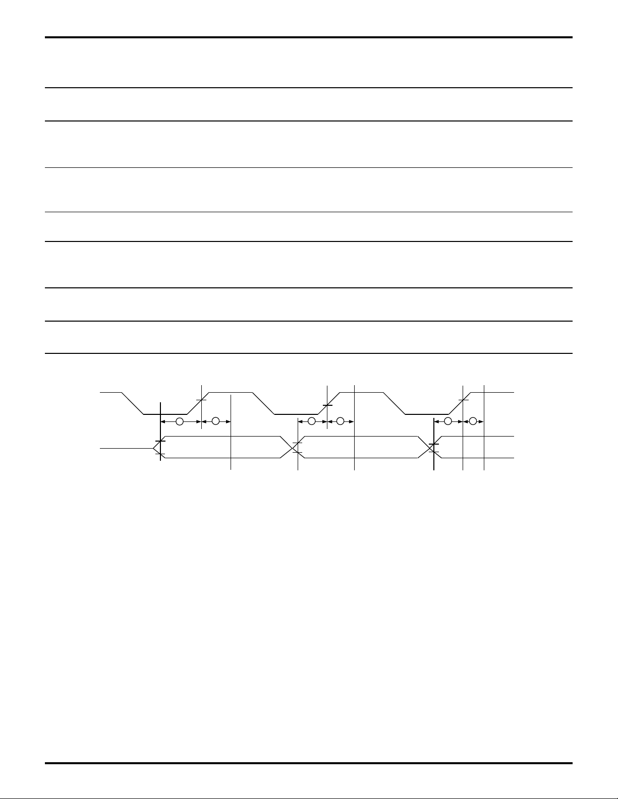
/RD (MPU)
TxFIFO
Z80189/Z8L189
HINTR
THRE
/WR (Host)
THR
/RD (Host)
11R
17
16
18
Figure 26. Interrupt Timing Transmitter FIFO
DS971890301
23
Zilog
PRELIMINARY
GENERAL-PURPOSE EMBEDDED CONTROLLERS
16550 MIMIC TIMING (Continued)
Table 8. Interrupt Timing Transmitter FIFO Table
Z8L189-20 MHz Z80189-33 MHz
No Sym Parameter Min Max Min Max Units
16 tHR Delay from /WR 2.5 2.5 phi cycles
(WR THR) to Reset
Interrupt
17 TSTI Delay from Stop to 2 2 phi cycles
Interrupt (THRE)
18 TIR Delay from /RD to 2.5 2.5 phi cycles
Reset Interrupt
Table 9. I/O Port Timing Table
Z8L189-20 MHz Z80189-33 MHz
No Sym Parameter Min Max Min Max Units
Z80189/Z8L189
1 TsPIA(WR) Data Setup Time to (Port) WR Fall 20 20 ns
2 TdWR(PIA) Data Valid Delay from WR Rise 60 60 ns
/WR
Port
1
2
Port (Output)
1 2 1 2
Port Output Data 1 (Out) Port Output Data 2 (Out)
Figure 27. I/O Port Timing Diagram
24
DS971890301

Zilog
PRELIMINARY
GENERAL-PURPOSE EMBEDDED CONTROLLERS
Z80189/Z8L189
PC DMA TIMING
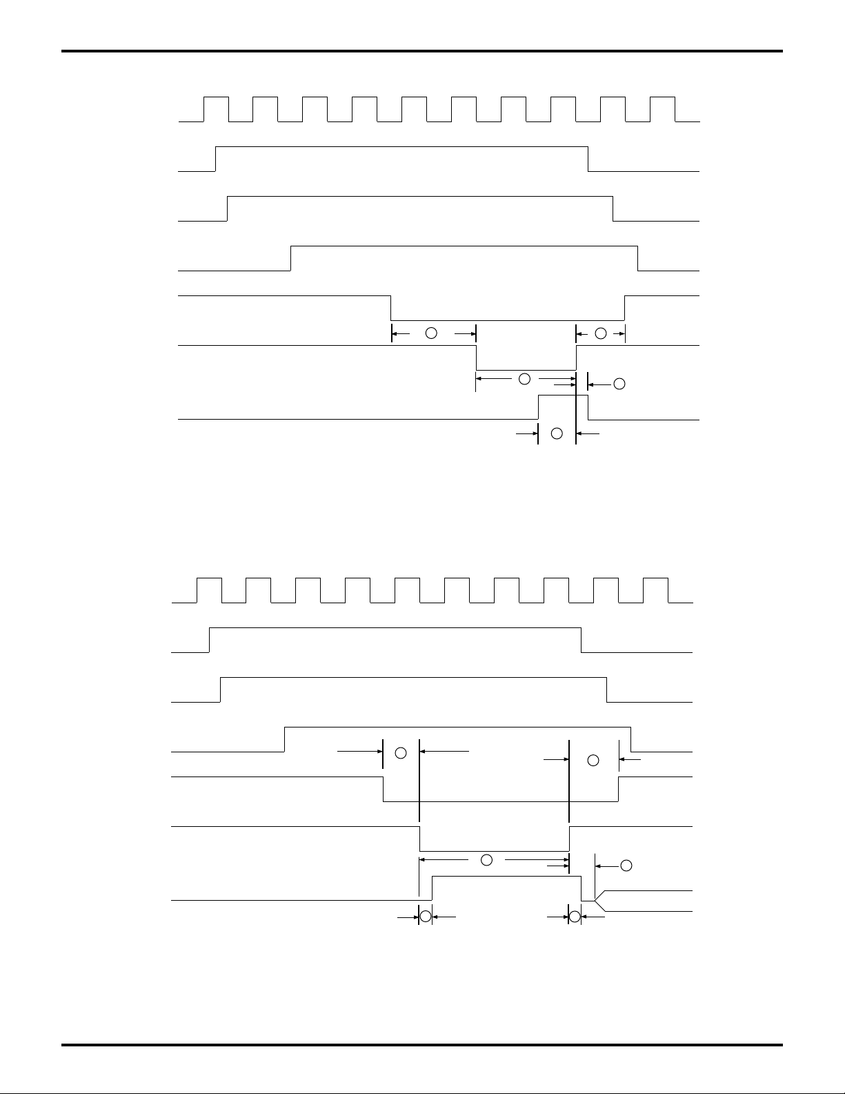
Table 10. PC DMA Mailbox Timing
PD DMA Write: Memory-Read, I/O Write DMA Bus Cycle
Z8L189-20 MHz Z80189-33 MHz
No Sym Parameter Min Max Min Max Units
1 tACKWh /HDACK Active Hold 144 144 ns
/HWR Inactive
2 tWRs /HDACK Active to 301 301 ns
/HWR Active
3 tWR /HWR Active to 454 454 ns
Inactive
4 tvWR Data Valid to /HWR 133 133 ns
Inactive
5 tDWRh Write Data Valid Hold 25 25 ns
from /HWR Inactive
Table 11. PC DMA Mailbox Timing
PD DMA Read: I/O-Read, Memory-Write DMA Bus Cycle
Z8L189-20 MHz Z80189-33 MHz
No Sym Parameter Min Max Min Max Units
1 tACKRh /HDACK Active Hold 89 89 ns
/HRD Inactive
2 tRDs /HDACK Active to 62 62 ns
/HRD Active
3 tRD /HRD Active to 749 749 ns
Inactive
4 tvRD Data Valid from /HRD 215 215 ns
Active
5 tDRDh Read Data Valid Hold 0 0 ns
from /HRD Inactive
6 tDZ Data Float from /HRD 50 50 ns
Inactive
DS971890301
25
Zilog
PC DMA TIMING DIAGRAMS
PC Clock
Internal
HDRQR
HDRQ
/AEN
/HDACK
PRELIMINARY
GENERAL-PURPOSE EMBEDDED CONTROLLERS
Z80189/Z8L189
(1)
/HWR
HD [0:7]
Valid
PC Clock
Internal
HDRQR
HDRQ
(1) The HDRQ will not fall inactive until it ses the
falling edge of /HWR during the /HDACK cycle.
Figure 28. PC DMA Write: Memory-Read, I/O Write
DMA Bus Cycle on PC AT Bus
2
3
5
1
4
(1)
26
/AEN
/HDACK
/HRD
HD [0:7]
Valid
(1) The HDRQ will not fall inactive until it sees the
falling edge of /HRD during the /HDACK cycle.
2
3
4
5
Figure 29. PC DMA Read: I/O-Read, Memory-Write
DMA Bus Cycle on PC AT Bus
1
6
DS971890301

Zilog
PIN DESCRIPTION
CPU Signals
PRELIMINARY
GENERAL-PURPOSE EMBEDDED CONTROLLERS
Z80189/Z8L189
A19-A0. Address Bus (Input/Output, active High, tri-state).
A0-A19 form a 20-bit address bus. The Address Bus
provides the address for memory data bus exchanges, up
to 1 Mbyte, and I/O data bus exchanges, up to 64K. The
address bus enters a high impedance state during reset
and external bus acknowledge cycles, as well as during
SLEEP and HALT states. This bus is an input when the
external bus master is accessing the on-chip peripherals.
D7-D0. Data Bus (Bidirectional, active High, tri-state). D0D7 constitute an 8-bit bidirectional data bus, used for the
transfer of information to and from I/O and memory devices. The data bus enters the high impedance state
during reset and external bus acknowledge cycles, as well
as during SLEEP and HALT states.
/RD. Read (Input/Output, active Low, tri-state). /RD indicates that the CPU wants to read data from memory or an
I/O device. The addressed I/O or memory device should
use this signal to gate data onto the CPU data bus.
/WR. Write (Output, active Low, tri-state). /WR indicates
that the CPU data bus holds valid data to be stored at the
addressed I/O or memory location.
/IORQ. I/O Request (Input/Output, active Low, tri-state).
/IORQ indicates that the address bus contains a valid I/O
address for an I/O read or I/O write operation. /IORQ is also
generated, along with /M1, during the acknowledgment of
the /INT0 input signal to indicate that an interrupt response
vector can be placed onto the data bus.
/M1. Machine Cycle 1 (Input/Output, active Low). Together
with /MREQ, /M1 indicates that the current cycle is the
opcode fetch cycle of an instruction execution. Together
with /IORQ, /M1 indicates that the current cycle is for an
interrupt acknowledge. It is also used with the /HALT and
ST signal to decode status of the CPU machine cycle.
/MREQ. Memory Request (Input/Output, active Low, tristate). /MREQ indicates that the address bus holds a valid
address for a memory read or memory write operation.
/WAIT. (Input, active Low). /WAIT indicates to the MPU that
the addressed memory or I/O devices are not ready for a
data transfer. This input is used to induce additional clock
cycles into the current machine cycle. The /WAIT input is
sampled on the falling edge of t2 (and subsequent wait
states). If the input is sampled low, then additional wait
states are inserted until the /WAIT input is sampled high, at
which time execution will continue.
/HALT. Halt/Sleep Status (Output, active Low). This output
is asserted after the CPU has executed either the HALT or
SLP instruction, and is waiting for either non-maskable or
maskable interrupt before operation can resume. It is also
used with the /M1 and ST signals to decode status of the
CPU machine cycle. On exit of Halt/Sleep, the first instruction fetch is delayed 16 clock cycles after the /HALT pin
goes high.
/BUSACK. Bus Acknowledge (Output, active Low
tri-state). /BUSACK indicates to the requesting device, the
MPU address and data bus, and some control signals,
have entered their high-impedance state.
/BUSREQ. Bus Request (Input, active Low). This input is
used by external devices (such as DMA controllers) to
request access to the system bus. This request has a
higher priority than /NMI and is always recognized at the
end of the current machine cycle. This signal will stop the
CPU from executing further instructions and places the
address and data buses, and other control signals, into the
high impedance state.
/NMI. Non-maskable interrupt (Input, negative edge triggered). /NMI has a higher priority than /INT and is always
recognized at the end of an instruction, regardless of the
state of the interrupt enable flip-flops. This signal forces
CPU execution to continue at location 0066H.
/INT0. Maskable Interrupt Request 0 (Input, active Low).
This signal is generated by external I/O devices. The CPU
will honor this request at the end of the current instruction
cycle as long as the /NMI and /BUSREQ signals are
inactive. The CPU acknowledges this interrupt request
with an interrupt acknowledge cycle. During this cycle,
both the /M1 and /IORQ signals will become active.
/INT1, /INT2. Maskable Interrupt Requests 1 and 2 (inputs,
active Low). This signal is generated by external I/O
devices. The CPU will honor these requests at the end of
the current instruction cycle as long as the /NMI, /BUSREQ,
and /INT0 signals are inactive. The CPU will acknowledge
these interrupt requests with an interrupt acknowledge
cycle. Unlike the acknowledgment for /INT0, during this
cycle neither the /M1 or /IORQ signals will become active.
These pins may be programmed to provide active low
level, rising or falling edge interrupts. The level of the
external /INT1 and /INT2 pins may be read through bits
PC6 and PC7 of parallel port C.
DS971890301
27

Zilog
PIN DESCRIPTION (Continued)
PRELIMINARY
GENERAL-PURPOSE EMBEDDED CONTROLLERS
Z80189/Z8L189
/RFSH. Refresh (Output, active Low, tri-state). Together
with /MREQ,/RFSH indicates that the current CPU machine
cycle and the contents of the address bus should be used
for refresh of dynamic memories. The low order 8 bits of the
address bus (A7-A0) contain the refresh address.
/MRD. Memory Read (Output, active Low, tri-state). /MRD
is active when both the internal /MREQ and /RD signals are
active.
/MWR. Memory write (output, active Low, tri-state). /MWR
is active when both the internal /MREQ and /WR signals are
active.
Z180™ MPU UART and SIO Signals
CKA0, CKA1. Asynchronous Clock 0 and 1 (Bidirectional,
active High). When in output mode, these pins are
the transmit and receive clock outputs from the ASCI
baud rate generators. When in input mode, these pins
serve as the external clock inputs for the ASCI baud rate
generators.
CKS. Serial Clock (Bidirectional, active High). This line is
the clock for the CSIO channel.
/DCD0. Data Carrier Detect 0 (Input, active Low). This is a
programmable modem control signal for ASCI channel 0.
/RTS0. Request to Send 0 (Output, active Low, tri-state).
This is a programmable modem control signal for ASCI
channel 0.
/CTS0/CTS1. Clear to Send 0 (Input, active Low). This line
is a modem control signal for the ASCI channel 0 and 1.
Z180™ MPU DMA Signals
/TEND0. Transfer End 0 (outputs, active Low). This output
is asserted active during the last write cycle of a DMA
operation. It is used to indicate the end of the block
transfer.
/DREQ0, /DREQ1. DMA request 0 and 1 (Input, active
Low). /DREQ is used to request a DMA transfer from one
of the on-chip DMA channels. The DMA channels monitor
these inputs to determine when an external device is ready
for a read or write operation. These inputs can be programmed to be either level or edge sensed.
Z180™ MPU Timer Signals
T
. Timer Out (Output, active High). T
OUT
output from PRT channel 1. This line is multiplexed with
HINTR1 of the 16550 MIMIC.
is the pulse
OUT
16550 MIMIC Interface Signals
HD7-HD0. Host Data Bus (Input/Output, tri-state). In
Z80189, the host data bus is used to communicate between the 16550 MIMIC interface and the PC/XT/AT. It is
multiplexed with the PA7-PA0 of parallel port A.
/HDDIS. Host Driver Disable (Output, active Low). In
Z80189, this signal goes low whenever the PC/XT/AT is
reading data from the 16550 MIMIC interface. The /HDDIS
pin should also go active low on each PC DMA read cycle.
HA2-HA0. Host Address (Input). In Z80189, these pins are
the address inputs to the 16550 MIMIC interface. This
address determines which register the PC/XT/AT accesses.
TXA0. Transmit Data 0 (Output, active High). This signal is
the transmitted data from the ASCI channel 0.
TXS. Clocked Serial Transmit Data (Output, active High).
This line is the transmitted data from the CSIO channel.
RXA0. Receive Data 0 (Input, active High). This signal is
the receive data to ASCI channel 0.
RXS. Clocked Serial Receive Data (Input, active High).
This line is the receiver data for the CSIO channel.
RXA1. Received Data ASCI Channel 1.
TXA1. Transmitted Data ASCI Channel 1.
28
HA9-HA3, HAEN. Host COM Port Decode Address (Input). In Z80189, these pins are multiplexed when COM
Port Decode is enabled (default). These pins are used to
provide internal MIMIC Enable when HA9-HA3 match the
programmed MIMIC address field. HAEN is also used to
access the PC DMA Mailbox registers.
/HCS. Host Chip Select (Input, active Low). In Z80189, this
input is used by the PC/XT/AT to select the 16550 MIMIC
interface for an access. The /HCS input is disabled when
using the internal COM Port Decoder. When setting the
/HCS Force bit in the CDR register, the /HCS output is
asserted when HA3-HA9 is within the boundaries programmed by bits 3-4 of the CDR register and /HRD or
/HWR is asserted. /HCS is NOT asserted for PC DMA
Mailbox accesses.
DS971890301

Zilog
PRELIMINARY
GENERAL-PURPOSE EMBEDDED CONTROLLERS
Z80189/Z8L189
/HWR. Host Write (Input, active Low). In Z80189, this input
is used by the PC/XT/AT to signal the 16550 MIMIC
interface that a write operation is taking place.
/HRD. Host Read (Input, active Low). In Z80189, this input
is used by the PC/XT/AT to signal the 16550 MIMIC
interface that a read operation is taking place.
HINTR1, HINTR2. Host Interrupt (Output, active High tristate). In Z80189, this output is used by the 16550 MIMIC
interface to signal the PC/XT/AT that an interrupt is pending. In Z80189 COM Port Decode mode, the MIMIC interrupt request can be routed to either HINTR1 or 2 depending on the COM Port Decode selected. The deselected
HINTR line will be forced to tri-state, while the selected
HINTR will follow what is programmed in the MIMIC Master
Control Register.
HC1, HC2. Host COM Select Pin 1&2 (Input). HC1 and HC2
are general-purpose inputs that can be used for COM Port
selection. The status of these pins are read by use of the
CDR register. The status of these pins can be used by
firmware to select the appropriate COM Port address
decode range.
PC7-PC0. Parallel Port C (Input/Output). These lines can
be configured as inputs or outputs on a bit by bit basis for
bits PC5-PC0. Bits PC7 and PC6 are input only and read
the level of the external /INT2 and /INT1 pins. When /INT2
and/or /INT1 are in edge capture mode writing a ‘1’ to the
respective PC7, PC6 bit clears the interrupt capture latch.
Writing a ‘0’ has no effect.
Emulation Signals
EV1, EV2. Emulation Select (Input). These two pins
determine the emulation mode the Z180 MPU is in. They
are as follows:
EV2 EV1
Mode 0 0 0 Normal mode, on-chip Z180 bus
master.
Mode 1 0 1 Emulation Adapter Mode
Mode 2 1 0 Emulator Probe Mode
Mode 3 1 1 Reserved
System Control Signals
PC DMA Mailbox Signals
/HDACK0, /HDACK1. Host DMA Acknowledge (Input,
active Low). This input signal indicates to the Z80189 that
the PC DMA controller has acknowledged the request and
will begin data transfer. /HDACK0 is multiplexed with
/CKA0 and /DREQ0. /HDACK1 is multiplexed with
/BUSREQ.
HDRQ0, HDRQ1. Host DMA Request (output, active high,
tri-state). This output requests to the PC DMA controller
that the Z80189 is ready for a DMA data transfer. HDRQ is
multiplexed with /RTS0. HDRQ1 is multiplexed with
/BUSACK.
Parallel Ports
PA7-PA0. Parallel Port A (Input/Output). These lines can
be configured as inputs or outputs on a bit-by-bit basis
when the Z80189 is operated in mode 0.
PB7-PB0. Parallel Port B (Input/Output). These lines can
be configured as inputs or outputs on a bit-by-bit basis
when the port function is selected in the System
Configuration register.
ST. Status (Output, active High). This signal is used with
the M1 and /HALT output to decode the status of the CPU
machine cycle.
/RESET. Reset Signal (Input, Active Low). /RESET signal
is used for initializing the MPU and other devices in the
system. It must be kept in the active state for a period of at
least 6 system clock cycles.
IEI. Interrupt Enable Signal (Input, active High). IEI is used
with the IEO to form a priority daisy chain when there is
more than one interrupt driven peripheral.
IE0. Interrupt Enable Output Signal (Output, active High).
In the daisy-chain interrupt control, IEO controls the interrupt
of external peripherals. IEO is active when IEI is “1” and the
CPU is not servicing an interrupt from the on-chip
peripherals. This pin is multiplexed with /IOCS1.
/IOCS1. I/O Chip Select 1 (output, active Low) is an
auxiliary chip select that decodes A7, A6, /IORQ, /M1 and
effectively decodes the address space XX80 to XXBF for
I/O transactions. A15 through A8 are not decoded so that
the chip select is active in all pages of I/O address space.
The /IOCS1 function is the default on power on or reset
condition and is changed by programming bit 2 in the
Interrupt Edge/Pin Mux Register.
DS971890301
29

Zilog
System Control Signals (Continued)
PRELIMINARY
GENERAL-PURPOSE EMBEDDED CONTROLLERS
Z80189/Z8L189
/IOCS2. I/O Chip Select 2 (output, active Low) This pin is
a secondary peripheral I/O chip select. This pin is active for
I/O accesses between XXC0H to XXC7H or XXC8H to
XXCFH (programmable by bit 1 of the IOBRG register).
/RAMCS. RAM Chip Select (Output, active Low). Signal
used to access RAM based upon the address and the
RAMLBR and RAMUBR registers.
/ROMCS. ROM Chip Select (Output, active Low). Signal
used to access ROM based upon the address and the
ROMBR register.
XTAL. Crystal (Output, active High). Crystal oscillator
connection. This pin should be left open if an external clock
PIN MULTIPLEXING
To allow for COM Port decode and omission of ESCC core,
Pin Multiplexing is changed with respect to the Z182.
ESCC CH.A pins will be replaced by COM Decode and
ASCI CH.A pins as follows:
RxDA → HA6
/TRxCA → HAEN
TxDA → HINTR2
DCDB → /HRD//DCD0
/CTSB → /HWR//CTS0
is used instead of a crystal. The oscillator input is not a TTL
level (reference DC characteristics).
EXTAL. External Clock/Crystal (Input, active High). Crystal
oscillator connections. An external clock can be input to
the Z80189 on this pin when a crystal is not used. This input
is Schmitt-triggered.
PHI. System Clock (Output, active High). The output is
used as a reference clock of the MPU and the external
system.
VCC. Power Supply. +5 Volts
VSS. Power Supply. 0 Volts
When COM decode bit is set (enabled during reset) the
following pins become multiplexed as follows.
/RFSH → HA3
/WAIT → HA4
/DREQ1 → HA5
/HA6 → HA6
IEI → HA7
/HA8 → HA8
CKA1/TEND0 → HA9
/HAEN → HAEN
Note that ASCI channel 0 functions can be found in two
places. These pins are ORed with ASCI channel 0 functions that are multiplexed with Port B (pins 35-39 QFP).
/DCD0, /CTS0, RXA0 inputs will come from 78, 79, 81
(respectively) when Port B (0-4) is enabled. When MIMIC
is disabled, /HDDIS pin doubles as TXA0 output. Note that
/RTS0 has also been changed to pin 50.
These pins are selected such that they are all high-z inputs
at power up to prevent any problems with connecting
address lines directly to PC bus. Although, the COM
decode multiplexing is enabled on power-up, the COM
address decoding is disabled.
30
DS971890301
 Loading...