

FEATURES
PRELIMINARY
P
RELIMINARY
C
USTOMER PROCUREMENT SPECIFICATION
Z86E73/E74 32K OTP
Z86L73/L74 32K ROM
INFRARED REMOTE CONTROLLERS
Z86E73/E74/L73/L74
CP95LVO0801
ROM RAM* One-Time Speed
Part (Kbyte) (Kbyte) Programmable (MHz)
Z86E73 32 1004 Yes 8
Z86L73 32 492 No 8
Z86E74 32 1004 Yes 8
Z86L74 32 1004 No 8
* General-Purpose
■ 40-Pin DIP, 44-Pin PLCC/QFP Packages (E73/L73)
64-Pin DIP, 68-Pin PLCC Packages (E74/L74)
■ 2.0V to 3.9V Operating Range (L73/L74)
4.5V to 5.5V Operating Range (E73/E74)
■ Low-Power Consumption
(Typical: 40 mw for L73/L74)
(Typical: 60 mw for E73/E74)
■ 0°C to +70°C Temperature Range
■ Expanded Register Files (ERF)
■ 31 Input/Output Lines (E73/L73)
51 Input/Output Lines (E74/L74*)
*Note: With Auto Latch on Port 4, 5 and 6.
■ Five Prioritized Interrupts with Programmable Polarity
■ Two Comparators
■ 8-Bit Counter/Timer with Two Capture Registers and
16-Bit Counter/Timer with One Capture Register
■ Watch-Dog Timer (WDT)/Power-On Reset (POR)
■ On-Chip Oscillator that Accepts a Crystal, Ceramic
Resonator, LC, RC, or External Clock Drive
■ Low-Voltage Detection and Protection
■ 32-KHz Mask Option to Disable Internal Feedback
Resistor (L73/L74)
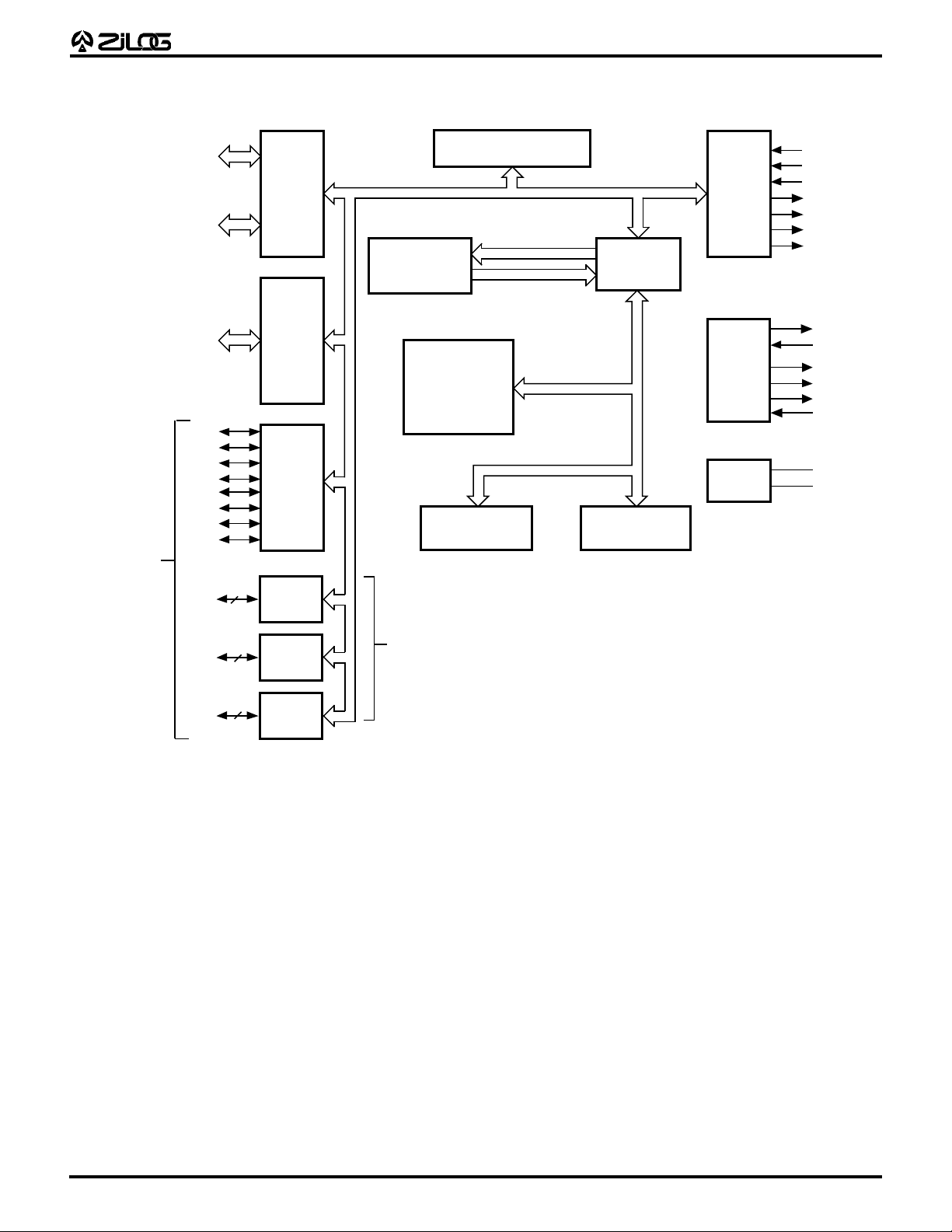
GENERAL DESCRIPTION
The Z86E73/L73/E74/L74 are ROM-based members of
Zilog's Z8® single-chip microcontroller family of infrared
(IR) consumer controller processors featuring fast and
flexible code execution. The Z86E73/E74 devices offer a
one-time programmable (OTP) option.
For applications demanding powerful I/O capabilities, the
Z86E73/L73's dedicated input and output lines are grouped
into four ports, and into seven ports for the Z86E74/L74.
They are configurable under software control to provide
timing, status signals, or parallel I/O.
Four address spaces, the Program Memory, Register File,
Data Memory, and Expanded Register File (ERF) support
a wide range of memory configurations. Through the ERF
the designer has access to three additional control registers
that provide extra peripheral devices, I/O ports, and register
addresses.
CP95LVO0801
Two on-chip counter/timers, with a large number of
selectable modes, offload the system of administering
real-time tasks such as counting/timing and I/O
datacommunications.
Notes:
All Signals with a preceding front slash, "/", are active Low, e.g.,
B//W (WORD is active Low); /B/W (BYTE is active Low, only).
Power connections follow conventional descriptions below:
Connection Circuit Device
Power V
Ground GND V
CC
V
DD
SS
1
PRELIMINARY
GENERAL DESCRIPTION (Continued)
Z86E73/E74/L73/L74
CP95LVO0801
I/O Bit
Programmable
P00
P01
P02
P03
P04
P05
P06
P07
P10
P11
P12
P13
P14
P15
P16
P17
P20
P21
P22
P23
P24
P25
P26
P27
Register File
4
Port 0
4
8
Port 1
Port 2
Register Bus
ROM
16K/32K x 8
512 or 1K x 8-bit
Address Bus
Internal Data Bus
Extended
Register
File
Counter/Timer 8
8-Bit
Internal
Extended
Register Bus
Counter/Timer 16
Port 3
Z8 Core
Machine
Timing
&
Instruction
Control
Power
16-Bit
P31
P32
P33
P34
P35
P36
P37
XTAL
/AS
/DS
R/W
/RESET
VDD
VSS
Port 4
8
Z86E74/L74
Port 5
8
Port 6
4
version only
Functional Block Diagram
2
PIN DESCRIPTION
PRELIMINARY
Z86E73/E74/L73/L74
CP95LVO0801
R//W
P25
P26
P27
P04
P05
P06
P14
P15
P07
VDD
P16
P17
XTAL2
XTAL1
P31
P32
P33
P34
/AS
1
2
3
4
5
6
7
8
9
10
11
12
13
14
15
16
17
18
19
20
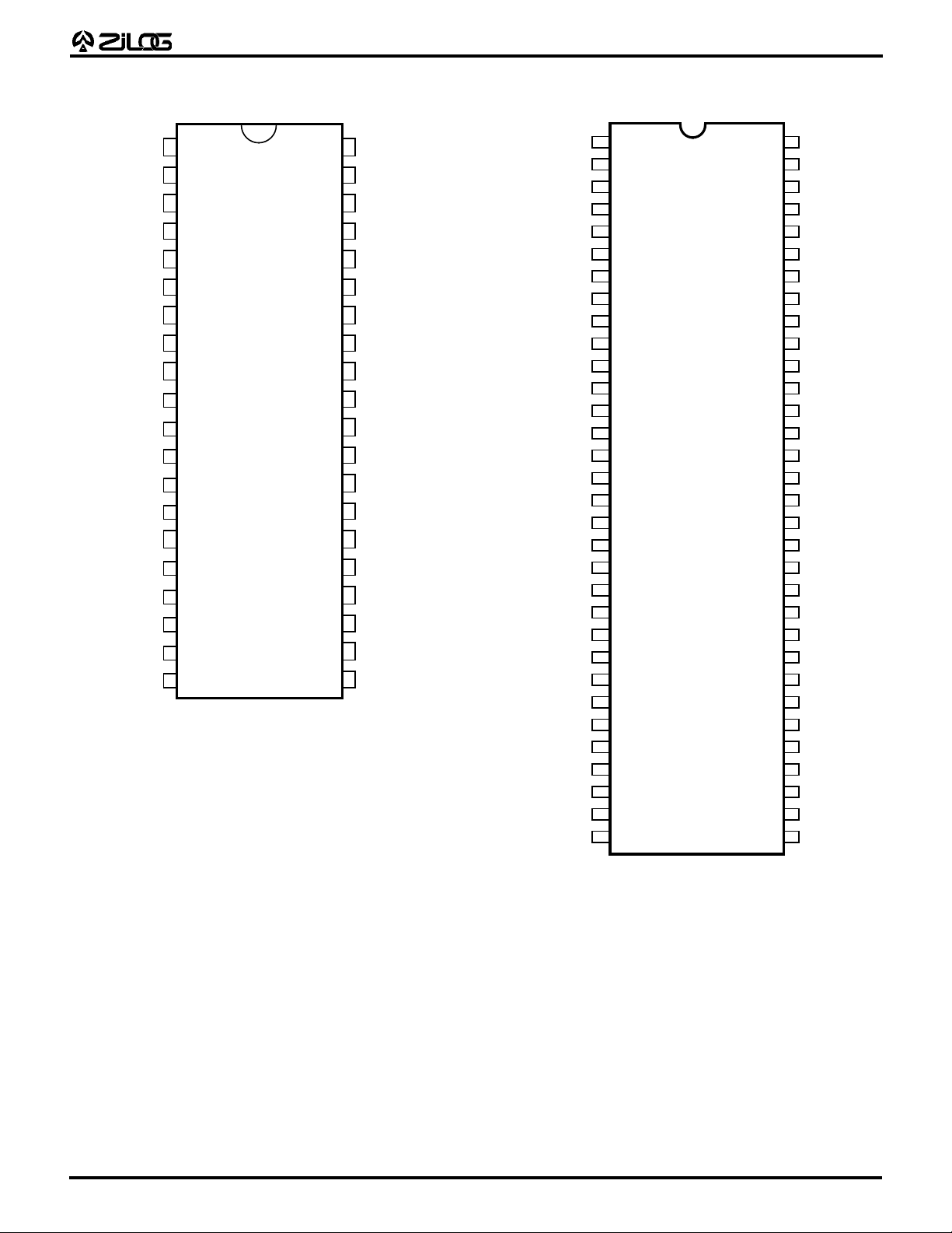
Z86E73/L73
DIP
40
39
38
37
36
35
34
33
32
31
30
29
28
27
26
25
24
23
22
21
Z86E73 (Standard Mode)
Z86L73 40-Pin DIP
Pin Assignments
/DS
P24
P23
P22
P21
P20
P03
P13
P12
VSS
P02
P11
P10
P01
P00
Pref1
P36
P37
P35
/RESET
P56
R/W
P25
P26
P27
P04
P05
P06
P14
P15
P07
VDD
VDD
P40
P41
P42
P43
P44
P45
P16
P17
XTAL2
XTAL1
P31
P32
P33
P34
P60
P61
/AS
P63
P55
1
2
3
4
5
6
7
8
9
10
11
12
13
14
15
16
17
18
19
20
21
22
23
24
25
26
27
28
29
30
31
32
Z86E74/L74
DIP
64
63
62
61
60
59
58
57
56
55
54
53
52
51
50
49
48
47
46
45
44
43
42
41
40
39
38
37
36
35
34
33
R//RL
P54
P53
/DS
P51
P50
P24
P23
P22
P21
P20
P03
P13
P12
VSS
VSS
P52
P57
P02
P46
P47
P11
P10
P01
P00
PREF1
P36
P37
P35
/RESET
VSS
P62
Z86E74 (Standard Mode)
Z86L74 64-Pin DIP
Pin Assignments
3
PIN DESCRIPTION
P21
P22
P23
P24
/DS
R//RL
R//W
P25
P26
P27
P04
PRELIMINARY
P20
P03
P13
P12
VSS
VSS
P02
P11
P10
P01
6543214443424140
7
8
9
10
11
12
13
14
15
16
17
18 19 20 21 22 23 24 25 26 27 28
P05
P06
P14
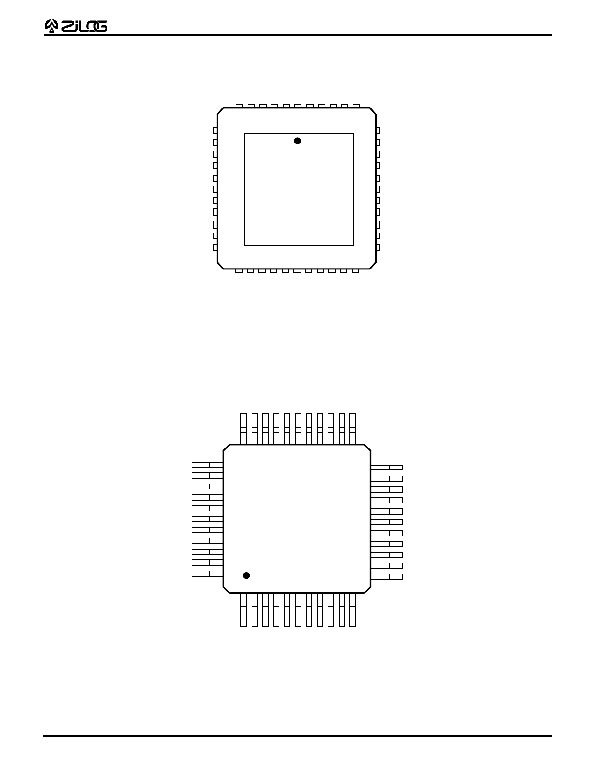
Z86E73/L73
PLCC
P15
P07
VDD
VDD
P16
P17
XTAL2
P00
39
38
37
36
35
34
33
32
31
30
29
XTAL1
Z86E73/E74/L73/L74
CP95LVO0801
Pref1
P36
P37
P35
/RESET
VSS
/AS
P34
P33
P32
P31
P21
P22
P23
P24
/DS
R//RL
R//W
P25
P26
P27
P04
Z86E73 (Standard Mode)
Z86L73 44-Pin PLCC
Pin Assignments
P20
P03
P13
P12
VSS
VSS
P02
P11
P10
33 32 31 30 29 2827 26 25 24 23
34
35
36
37
38
39
40
41
42
43
44
1234567891011
Z86E73/L73
QFP
P01
P00
22
21
20
19
18
17
16
15
14
13
12
Pref1
P36
P37
P35
/RESET
VSS
/AS
P34
P33
P32
P31
P05
P06
P14
P15
P07
VDD
VDD
P16
P17
XTAL2
XTAL1
Z86E73 (Standard Mode)
Z86L73 44-Pin QFP
Pin Assignments
4
PIN DESCRIPTION (Continued)
10
P21
11
P22
12
P23
13
P24
14
P50
15
P51
16
/DS
17
P53
18
P54
P56
R//W
N/C
P25
P26
P27
P04
19
20
21
22
23
24
25
26
R//RL
PRELIMINARY
P02
P57
P13
P20
P03
P12
VSS
VSS
789 6543216867666564636261
N/C
N/C
P52
P46
P47
Z86E74/L74
PLCC
27 28 29 30 31 32 33 34 35 36 37 38 39 40 41 42 43
P06
P14
P15
P05
P07
VDD
VDD
P40
P41
P42
P43
P44
P45
P01
P10
P11
P16
P17
XTAL2
P00
XTAL1
Z86E73/E74/L73/L74
CP95LVO0801
60
PREF1
59
P36
58
P37
57
P35
56
/RESET
55
VSS
54
P62
53
P55
52
N/C
51
P63
50
/AS
49
P61
48
P60
47
P34
46
P33
45
P32
44
P31
Z86E74 (Standard Mode)
Z86L74 68-Pin PLCC Pin Assignments
5
ABSOLUTE MAXIMUM RATINGS
PRELIMINARY
Z86E73/E74/L73/L74
CP95LVO0801
Symbol Description Min Max Units
V
CC
T
STG
T
A
Notes:
* Voltage on all pins with respect to GND.
† See Ordering Information.
Supply Voltage (*) –0.3 +7.0 V
Storage Temp. –65° +150° C
Oper. Ambient Temp. † C
STANDARD TEST CONDITIONS
The characteristics listed below apply for standard test
conditions as noted. All voltages are referenced to GND.
Positive current flows into the referenced pin (Test Load).
Stresses greater than those listed under Absolute Maximum Ratings may cause permanent damage to the device. This is a stress rating only; operation of the device at
any condition above those indicated in the operational
sections of these specifications is not implied. Exposure to
absolute maximum rating conditions for an extended
period may affect device reliability.
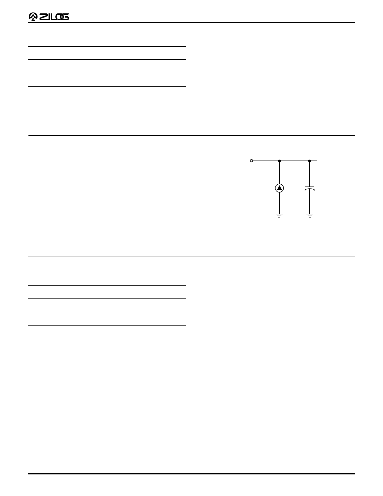
From Output
Under Test
I
150 pF
CAPACITANCE
TA = 25°C, VCC = GND = 0V, f = 1.0 MHz, unmeasured pins returned to GND.
Parameter Max
Input capacitance 12 pF
Output capacitance 12 pF
I/O capacitance 12 pF
Test Load Diagram
6

PRELIMINARY
DC CHARACTERISTICS (Z86E73/E74)
TA = 0°C to +70°C Typ @
Sym Parameter V
Max Input Voltage 4.0V 7 V IIN 250 µA
V
Clock Input 4.0V 0.9 V
CH
High Voltage Clock Generator
CC
5.5V 7 V IIN 250 µA
5.5V 0.9 V
Min Max 25°C Units Conditions Notes [3]
VCC + 0.3 V Driven by External
CC
VCC + 0.3 V Driven by External
CC
Z86E73/E74/L73/L74
CP95LVO0801
Clock Generator
V
Clock Input 40V VSS – 0.3 0.2 V
CL
CC
V Driven by External
Low Voltage Clock Generator
5.5V VSS– 0.3 0.2 V
CC
V Driven by External
Clock Generator
V
V
V
Input High Voltage 4.0V 0.7 V
IH
5.5V 0.7 V
Input Low Voltage 4.0V VSS – 0.3 0.2 V
IL
5.5V VSS – 0.3 0.2 V
Output High Voltage 4.0V VCC – 0.4 1.7 V IOH = –0.5 mA
OH1
VCC + 0.3 1.3 V
CC
VCC + 0.3 2.5 V
CC
CC
CC
0.5 V
0.9 V
5.5V VCC – 0.4 3.7 V IOH = –0.5 mA
V
V
Output High Voltage 4.0V 0.7 V IOH = –7 mA [10]
OH2
(P36, P37) 5.5V 0.7 V I
Output Low Voltage 4.0V 0.4 0.2 V IOL = 1.0 mA
OL1
,= –7 mA [10]
OH
5.5V 0.4 0.1 V IOL = 4.0 mA
V
Output Low Voltage 4.0V 0.8 0.3 V I
OL2
= 2.0 mA
OL
3 Pin Max
5.5V 0.8 0.5 V IOL = 8.0 mA
3 Pin Max
V
Output Low Voltage 4.0V 0.8 0.3 V I
OL2
= 10 mA [9]
OL
(P20-P22, P36,
P00, P01, P07) 5.5V 0.8 0.5 V I
= 10 mA [9]
OL
2 O/P only
V
V
V
I
IL
I
OL
I
IR
I
CC
Reset Input 4.0V 0.8 V
RH
High Voltage 5.5V 0.8 V
Reset Input 4.0V VSS – 0.3 0.2 V
Rl
Low Voltage 5.5V VSS – 0.3 0.2 V
Comparator Input 4.0V 25 10 mV
OFFSET
V
CC
CC
CC
V
CC
CC
CC
1.5 V
3.0 V
0.5
0.9
Offset Voltage 5.5V 25 10 mV
Input Leakage 4.0V –1 1 < 1 µAV
5.5V –1 1 < 1 µAV
Output Leakage 4.0V –1 1 < 1 µAV
5.5V –1 1 < 1 µAV
= OV, V
IN
= OV, V
IN
= OV, V
IN
= OV, V
IN
CC
CC
CC
CC
Reset Input Current 4.0V –45 –20 µA
5.5V –55 –30 µA
Supply Current 4.0V 10 4 mA @ 8.0 MHz [4, 5]
5.5V 15 10 mA @ 8.0 MHz [4, 5]
4.0V 100 10 µA @ 32 kHz [4, 5,11]
5.5V 300 10 µA @ 32 kHz [4, 5,11]
7

PRELIMINARY
DC CHARACTERISTICS (Z86E73/E74) (Continued)
TA = 0°C to +70°C Typ @
Sym Parameter V
CC
Min Max 25°C Units Conditions Notes [3]
Z86E73/E74/L73/L74
CP95LVO0801
I
Standby Current 4.0V 3 1 mA HALT Mode [4,5]
CC1
VIN = OV, V
CC
@ 8.0 MHz
5.5V 5 4 mA HALT Mode [4,5]
VIN = OV, V
CC
@ 8.0 MHz
4.0V 2 0.8 mA Clock Divide-by-16 [4,5]
@ 8.0 MHz
5.5V 4 2.5 mA Clock Divide-by-16 [4,5]
@ 8.0 MHz
I
Standby Current 4.0V 8 2 µA STOP Mode [6,8]
CC2
VIN = OV, V
CC
WDT is not Running
5.5V 10 3 µA STOP Mode [6,8]
VIN = OV, V
CC
WDT is not Running
4.0V 500 310 µA STOP Mode [6,8]
VIN = OV, V
CC
WDT is Running
5.5V 800 600 µA STOP Mode [6,8]
VIN = OV, V
CC
WDT is Running
T
Power-On Reset 4.0V 15 75 13 ms
POR
5.5V 5 20 7 ms
V
VCC Low Voltage Protection 3.3 2.75 V 8 MHz max [7]
LV
Ext. CLK Freq.
Notes:
[1] I
CC1
Crystal/Resonator 3.0 mA 5 mA 8.0 MHz
External Clock Drive 0.3 mA 5 mA 8.0 MHz
[2] GND = 0V.
[3] 4.0V to 5.5V.
[4] All outputs unloaded, I/O pins floating, inputs at rail.
[5] CL1 = CL2 = 100 pF.
[6] Same as note [4] except inputs at VCC.
[7] The VLV increases as the temperature decreases.
[8] Oscillator stopped.
[9] Two outputs at a time, independent to other outputs.
[10] One at a time.
[11] 32 kHz clock driver input.
Typ Max Unit Frequency
8
PRELIMINARY
DC CHARACTERISTICS (Z86L73/L74)
TA = 0°C to +70°C Typ @
Sym Parameter V
Max Input Voltage 2.0V 7 V IIN 250 µA
V
Clock Input 2.0V 0.9 V
CH
High Voltage Clock Generator
CC
3.9V 7 V IIN 250 µA
3.9V 0.9 V
Min Max 25°C Units Conditions Notes [3]
VCC + 0.3 V Driven by External
CC
VCC + 0.3 V Driven by External
CC
Z86E73/E74/L73/L74
CP95LVO0801
Clock Generator
V
Clock Input 2.0V VSS – 0.3 0.2 V
CL
CC
V Driven by External
Low Voltage Clock Generator
3.9V VSS– 0.3 0.2 V
CC
V Driven by External
Clock Generator
V
V
V
Input High Voltage 2.0V 0.7 V
IH
3.9V 0.7 V
Input Low Voltage 2.0V VSS – 0.3 0.2 V
IL
3.9V VSS – 0.3 0.2 V
Output High Voltage 2.0V VCC – 0.4 1.7 V IOH = –0.5 mA
OH1
VCC + 0.3 1.3 V
CC
VCC + 0.3 2.5 V
CC
CC
CC
0.5 V
0.9 V
3.9V VCC – 0.4 3.7 V IOH = –0.5 mA
V
V
Output High Voltage 2.0V 0.7 V IOH = –7 mA [10]
OH2
(P36, P37) 3.9V 0.7 V I
Output Low Voltage 2.0V 0.4 0.2 V IOL = 1.0 mA
OL1
,= –7 mA [10]
OH
3.9V 0.4 0.1 V IOL = 4.0 mA
V
Output Low Voltage 2.0V 0.8 0.3 V I
OL2
= 2.0 mA
OL
3 Pin Max
3.9V 0.8 0.5 V IOL = 8.0 mA
3 Pin Max
V
Output Low Voltage 2.0V 0.8 0.3 V I
OL2
= 10 mA [9]
OL
(P20-P22, P36,
P00, P01, P07) 3.9V 0.8 0.5 V I
= 10 mA [9]
OL
2 O/P only
V
V
V
I
IL
I
OL
I
IR
I
CC
Reset Input 2.0V 0.8 V
RH
High Voltage 3.9V 0.8 V
Reset Input 2.0V VSS – 0.3 0.2 V
Rl
Low Voltage 3.9V VSS – 0.3 0.2 V
Comparator Input 2.0V 25 10 mV
OFFSET
V
CC
CC
CC
V
CC
CC
CC
1.5 V
3.0 V
0.5
0.9
Offset Voltage 3.9V 25 10 mV
Input Leakage 2.0V –1 1 < 1 µAV
3.9V –1 1 < 1 µAVIN = OV, V
Output Leakage 2.0V –1 1 < 1 µAV
3.9V –1 1 < 1 µAV
= OV, V
IN
CC
IN
IN
= OV, V
= OV, V
CC
CC
CC
Reset Input Current 2.0V –45 –20 µA
3.9V –55 –30 µA
Supply Current 2.0V 10 4 mA @ 8.0 MHz [4, 5]
3.9V 15 10 mA @ 8.0 MHz [4, 5]
2.0V 100 10 µA @ 32 kHz [4, 5,11]
3.9V 300 10 µA @ 32 kHz [4, 5,11]
9
PRELIMINARY
DC CHARACTERISTICS (Z86L73/L74) (Continued)
TA = 0°C to +70°C Typ @
Sym Parameter V
CC
Min Max 25°C Units Conditions Notes [3]
Z86E73/E74/L73/L74
CP95LVO0801
I
Standby Current 2.0V 3 1 mA HALT Mode [4,5]
CC1
VIN = OV, V
CC
@ 8.0 MHz
3.9V 5 4 mA HALT Mode [4,5]
VIN = OV, V
CC
@ 8.0 MHz
2.0V 2 0.8 mA Clock Divide-by-16 [4,5]
@ 8.0 MHz
3.9V 4 2.5 mA Clock Divide-by-16 [4,5]
@ 8.0 MHz
I
Standby Current 2.0V 8 2 µA STOP Mode [6,8]
CC2
VIN = OV, V
CC
WDT is not Running
3.9V 10 3 µA STOP Mode [6,8]
VIN = OV, V
CC
WDT is not Running
2.0V 500 310 µA STOP Mode [6,8]
VIN = OV, V
CC
WDT is Running
3.9V 800 600 µA STOP Mode [6,8]
VIN = OV, V
CC
WDT is Running
T
Power-On Reset 2.0V 15 75 13 ms
POR
3.9V 5 20 7 ms
V
VCC Low Voltage Protection 2.15 1.7 V 8 MHz max [7]
LV
Ext. CLK Freq.
Notes:
[1] I
CC1
Crystal/Resonator 3.0 mA 5 mA 8.0 MHz
External Clock Drive 0.3 mA 5 mA 8.0 MHz
[2] GND = 0V.
[3] 2.0V to 3.9V.
[4] All outputs unloaded, I/O pins floating, inputs at rail.
[5] CL1 = CL2 = 100 pF.
[6] Same as note [4] except inputs at VCC.
[7] The VLV increases as the temperature decreases.
[8] Oscillator stopped.
[9] Two outputs at a time, independent to other outputs.
[10] One at a time.
[11] 32 kHz clock driver input.
Typ Max Unit Frequency
10

PRELIMINARY
AC CHARACTERISTICS
External I/O or Memory Read and Write Timing Diagram
R//W
Z86E73/E74/L73/L74
CP95LVO0801
Port 0, /DM
Port 1
/AS
/DS
(Read)
Port 1
12
16
8
3
13
19
20
A7 - A0 D7 - D0 IN
21
8 11
4
5
17
6
9
10
D7 - D0 OUTA7 - A0
14
7
15
/DS
(Write)
External I/O or Memory Read/Write Timing
11
PRELIMINARY
Z86E73/E74/L73/L74
CP95LVO0801
AC CHARACTERISTICS (Z86E73/E74)
External I/O or Memory Read and Write Timing Table
TA = 0°C to +70°C
V
CC
No. Symbol Parameter Note [3] Min Max Units Notes
1 TdA(AS) Address Valid to 4.0V 55 ns [2]
/AS Rising Delay 5.5V 55 ns
2 TdAS(A) /AS Rising to Address 2.0V 70 ns [2]
Float Delay 5.5V 70 ns
3 TdAS(DR) /AS Rising to Read 4.0V 400 ns [1, 2]
Data Required Valid 5.5V 400 ns
4 TwAS /AS Low Width 4.0V 80 ns [2]
5.5V 80 ns
5 Td Address Float to 4.0V 0 ns
/DS Falling 5.5V 0 ns
6 TwDSR /DS (Read) Low Width 4.0V 300 ns [1, 2]
5.5V 300 ns
7 TwDSW /DS (Write) Low Width 4.0V 165 ns [1, 2]
5.5V 165 ns
8 TdDSR(DR) /DS Falling to Read 4.0V 260 ns [1, 2]
Data Required Valid 5.5V 260 ns
8.0 MHz
9 ThDR(DS) Read Data to 4.0V 0 ns [2]
/DS Rising Hold Time 5.5V 0 ns
10 TdDS(A) /DS Rising to Address 4.0V 85 ns [2]
Active Delay 5.5V 95 ns
11 TdDS(AS) /DS Rising to /AS 4.0V 60 ns [2]
Falling Delay 5.5V 70 ns
12 TdR/W(AS) R//W Valid to /AS 4.0V 70 ns [2]
Rising Delay 5.5V 70 ns
13 TdDS(R/W) /DS Rising to 4.0V 70 ns [2]
R//W Not Valid 5.5V 70 ns
14 TdDW(DSW) Write Data Valid to /DS 4.0V 80 ns [2]
Falling (Write) Delay 5.5V 80 ns
15 TdDS(DW) /DS Rising to Write 4.0V 70 ns [2]
Data Not Valid Delay 5.5V 80 ns
16 TdA(DR) Address Valid to Read 4.0V 475 ns [1, 2]
Data Required Valid 5.5V 475 ns
17 TdAS(DS) /AS Rising to 4.0V 100 ns [2]
/DS Falling Delay 5.5V 100 ns
18 TdDM(AS) /DM Valid to /AS 4.0V 55 ns [2]
Falling Delay 5.5V 55 ns
19 TdDS(DM) /DS Rise to 4.0V 70 ns
/DM Valid Delay 5.5V 70 ns
20 ThDS(A) /DS Rise to Address 4.0V 70 ns
Valid Hold Time 5.5V 70 ns
Notes:
[1] When using extended memory timing add 2 TpC.
[2] Timing numbers given are for minimum TpC.
[3] 4.0V to 5.5V.
Standard Test Load.
All timing references use 0.9 VCC for a logic 1 and 0.1 VCC for a logic 0.
12

PRELIMINARY
Z86E73/E74/L73/L74
CP95LVO0801
AC CHARACTERISTICS (Z86L73/L74)
External I/O or Memory Read and Write Timing Table
TA = 0°C to +70°C
V
CC
No. Symbol Parameter Note [3] Min Max Units Notes
1 TdA(AS) Address Valid to 2.0V 55 ns [2]
/AS Rising Delay 3.9V 55 ns
2 TdAS(A) /AS Rising to Address 2.0V 70 ns [2]
Float Delay 3.9V 70 ns
3 TdAS(DR) /AS Rising to Read 2.0V 400 ns [1, 2]
Data Required Valid 3.9V 400 ns
4 TwAS /AS Low Width 2.0V 80 ns [2]
3.9V 80 ns
5 Td Address Float to 2.0V 0 ns
/DS Falling 3.9V 0 ns
6 TwDSR /DS (Read) Low Width 2.0V 300 ns [1, 2]
3.9V 300 ns
7 TwDSW /DS (Write) Low Width 2.0V 165 ns [1, 2]
3.9V 165 ns
8 TdDSR(DR) /DS Falling to Read 2.0V 260 ns [1, 2]
Data Required Valid 3.9V 260 ns
8.0 MHz
9 ThDR(DS) Read Data to 2.0V 0 ns [2]
/DS Rising Hold Time 3.9V 0 ns
10 TdDS(A) /DS Rising to Address 2.0V 85 ns [2]
Active Delay 3.9V 95 ns
11 TdDS(AS) /DS Rising to /AS 2.0V 60 ns [2]
Falling Delay 3.9V 70 ns
12 TdR/W(AS) R//W Valid to /AS 2.0V 70 ns [2]
Rising Delay 3.9V 70 ns
13 TdDS(R/W) /DS Rising to 2.0V 70 ns [2]
R//W Not Valid 3.9V 70 ns
14 TdDW(DSW) Write Data Valid to /DS 2.0V 80 ns [2]
Falling (Write) Delay 3.9V 80 ns
15 TdDS(DW) /DS Rising to Write 2.0V 70 ns [2]
Data Not Valid Delay 3.9V 80 ns
16 TdA(DR) Address Valid to Read 2.0V 475 ns [1, 2]
Data Required Valid 3.9V 475 ns
17 TdAS(DS) /AS Rising to 2.0V 100 ns [2]
/DS Falling Delay 3.9V 100 ns
18 TdDM(AS) /DM Valid to /AS 2.0V 55 ns [2]
Falling Delay 3.9V 55 ns
19 TdDS(DM) /DS Rise to 2.0V 70 ns
/DM Valid Delay 3.9V 70 ns
20 ThDS(A) /DS Rise to Address 2.0V 70 ns
Valid Hold Time 3.9V 70 ns
Notes:
[1] When using extended memory timing add 2 TpC.
[2] Timing numbers given are for minimum TpC.
[3] 2.0V to 3.9V.
Standard Test Load.
All timing references use 0.9 VCC for a logic 1 and 0.1 VCC for a logic 0.
13

AC CHARACTERISTICS
134
8
223
657
7
11
10
9
Additional Timing Diagram
Clock
T
IN
IRQ
N
PRELIMINARY
Z86E73/E74/L73/L74
CP95LVO0801
Clock
Setup
Stop
Mode
Recovery
Source
Additional Timing
14

PRELIMINARY
Z86E73/E74/L73/L74
CP95LVO0801
AC CHARACTERISTICS (Z86E73/E74)
Additional Timing Table
TA = 0°C to +70°C
V
CC
No Symbol Parameter Note [3] Min Max Units Notes
1 TpC Input Clock Period 4.0V 121 DC ns [1]
5.5V 121 DC ns [1]
2 TrC,TfC Clock Input Rise 4.0V 25 ns [1]
and Fall Times 5.5V 25 ns [1]
3 TwC Input Clock Width 4.0V 37 ns [1]
5.5V 37 ns [1]
4 TwTinL Timer Input 4.0V 100 ns [1]
Low Width 5.5V 70 ns [1]
5 TwTinH Timer Input 4.0V 3TpC [1]
High Width 5.5V 3TpC [1]
6 TpTin Timer Input Period 4.0V 8TpC [1]
5.5V 8TpC [1]
7 TrTin,TfTin Timer Input Rise 4.0V 100 ns [1]
and Fall Timers 5.5V 100 ns [1]
8A TwIL Interrupt Request 4.0V 100 ns [1, 2]
Low Time 5.5V 70 ns [1, 2]
8.0 MHz
8B TwIL Int. Request 4.0V 3TpC [1, 3]
Low Time 5.5V 3TpC [1, 3]
9 TwIH Interrupt Request 4.0V 3TpC [1, 2]
Input High Time 5.5V 3TpC [1, 2]
10 Twsm Stop-Mode Recovery 4.0V 12 ns [8]
Width Spec 5.5V 12 ns [8]
4.0V 5TpC [7]
5.5V 5TpC [7]
11 Tost Oscillator 4.0V 5TpC [4]
Start-up Time 5.5V 5TpC [4]
12 Twdt Watch-Dog Timer (5 ms) 4.0V 12 75 ms D0 = 0 [5]
Delay Time 5.5V 5 20 ms D1 = 0 [5]
(10 ms) 4.0V 25 150 ms D0 = 1 [5]
5.5V 10 40 ms D1 = 0 [5]
(20 ms) 4.0V 50 300 ms D0 = 0 [5]
5.5V 20 80 ms D1 = 1 [5]
(80 ms) 4.0V 225 1200 ms D0 = 1 [5]
5.5V 80 320 ms D1 = 1 [5]
Notes:
[1] Timing Reference uses 0.9 VCC for a logic 1 and 0.1 VCC for a logic 0.
[2] Interrupt request through Port 3 (P33-P31).
[3] Interrupt request through Port 3 (P30).
[4] SMR – D5 = 0.
[5] Reg. WDTMR.
[6] 4.0V to 5.5V.
[7] Reg. SMR – D5 = 0.
[8] Reg. SMR – D5 = 1.
15

PRELIMINARY
Z86E73/E74/L73/L74
CP95LVO0801
AC CHARACTERISTICS (Z86L73/L74)
Additional Timing Table
TA = 0°C to +70°C
V
CC
No Symbol Parameter Note [3] Min Max Units Notes
1 TpC Input Clock Period 2.0V 121 DC ns [1]
3.9V 121 DC ns [1]
2 TrC,TfC Clock Input Rise 2.0V 25 ns [1]
and Fall Times 3.9V 25 ns [1]
3 TwC Input Clock Width 2.0V 37 ns [1]
3.9V 37 ns [1]
4 TwTinL Timer Input 2.0V 100 ns [1]
Low Width 3.9V 70 ns [1]
5 TwTinH Timer Input 2.0V 3TpC [1]
High Width 3.9V 3TpC [1]
6 TpTin Timer Input Period 2.0V 8TpC [1]
3.9V 8TpC [1]
7 TrTin,TfTin Timer Input Rise 2.0V 100 ns [1]
and Fall Timers 3.9V 100 ns [1]
8A TwIL Interrupt Request 2.0V 100 ns [1, 2]
Low Time 3.9V 70 ns [1, 2]
8.0 MHz
8B TwIL Int. Request 2.0V 3TpC [1, 3]
Low Time 3.9V 3TpC [1, 3]
9 TwIH Interrupt Request 2.0V 3TpC [1, 2]
Input High Time 3.9V 3TpC [1, 2]
10 Twsm Stop-Mode Recovery 2.0V 12 ns [8]
Width Spec 3.9V 12 ns [8]
2.0V 5TpC [7]
3.9V 5TpC [7]
11 Tost Oscillator 2.0V 5TpC [4]
Start-up Time 3.9V 5TpC [4]
12 Twdt Watch-Dog Timer (5 ms) 2.0V 12 75 ms D0 = 0 [5]
Delay Time 3.9V 5 20 ms D1 = 0 [5]
(10 ms) 2.0V 25 150 ms D0 = 1 [5]
3.9V 10 40 ms D1 = 0 [5]
(20 ms) 2.0V 50 300 ms D0 = 0 [5]
3.9V 20 80 ms D1 = 1 [5]
(80 ms) 2.0V 225 1200 ms D0 = 1 [5]
3.9V 80 320 ms D1 = 1 [5]
Notes:
[1] Timing Reference uses 0.9 VCC for a logic 1 and 0.1 VCC for a logic 0.
[2] Interrupt request through Port 3 (P33-P31).
[3] Interrupt request through Port 3 (P30).
[4] SMR – D5 = 0.
[5] Reg. WDTMR.
[6] 2.0V to 3.9V.
[7] Reg. SMR – D5 = 0.
[8] Reg. SMR – D5 = 1.
16

AC CHARACTERISTICS
12345
6
7891011
Handshake Timing Diagrams
PRELIMINARY
Z86E73/E74/L73/L74
CP95LVO0801
Data In
/DAV
(Input)
RDY
(Output)
Data Out
/DAV
(Output)
Data In Valid
Delayed DAV
Input Handshake Timing
Data Out Valid
Next Data In Valid
Delayed RDY
Next Data Out Valid
Delayed DAV
RDY
(Input)
Delayed RDY
Output Handshake Timing
17

PRELIMINARY
Z86E73/E74/L73/L74
CP95LVO0801
AC CHARACTERISTICS (Z86E73/E74)
Handshake Timing Table
TA = 0°C to +70°C
V
CC
No Symbol Parameter Note [3] Min Max Direction
1 TsDI(DAV) Data In Setup Time 4.0V 0 IN
5.5V 0 IN
2 ThDI(DAV) Data In Hold Time 4.0V 160 IN
5.5V 115 IN
3 TwDAV Data Available Width 4.0V 155 IN
5.5V 110 IN
4 TdDAVI(RDY) DAV Falling to RDY 4.0V 160 IN
Falling Delay 5.5V 115 IN
5 TdDAVId(RDY) DAV Rising to RDY 4.0V 120 IN
Falling Delay 5.5V 80 IN
6 TdRDYO(DAV) RDY Rising to DAV 4.0V 0 IN
Falling Delay 5.5V 0 IN
7 TdDO(DAV) Data Out to DAV 4.0V 63 OUT
Falling Delay 5.5V 63 OUT
8 TdDAV0(RDY) DAV Falling to RDY 4.0V 0 OUT
Falling Delay 5.5V 0 OUT
8.0 MHz Data
9 TdRDY0(DAV) RDY Falling to DAV 4.0V 160 OUT
Rising Delay 5.5V 115 OUT
10 TwRDY RDY Width 4.0V 110 OUT
5.5V 80 OUT
11 TdRDY0d(DAV) RDY Rising to DAV 4.0V 110 OUT
Falling Delay 5.5V 80 OUT
Note:
[3] 4.0V to 5.5V.
18

PRELIMINARY
Z86E73/E74/L73/L74
CP95LVO0801
AC CHARACTERISTICS (Z86L73/L74)
Handshake Timing Table
TA = 0°C to +70°C
V
CC
No Symbol Parameter Note [3] Min Max Direction
1 TsDI(DAV) Data In Setup Time 2.0V 0 IN
3.9V 0 IN
2 ThDI(DAV) Data In Hold Time 2.0V 160 IN
3.9V 115 IN
3 TwDAV Data Available Width 2.0V 155 IN
3.9V 110 IN
4 TdDAVI(RDY) DAV Falling to RDY 2.0V 160 IN
Falling Delay 3.9V 115 IN
5 TdDAVId(RDY) DAV Rising to RDY 2.0V 120 IN
Falling Delay 3.9V 80 IN
6 TdRDYO(DAV) RDY Rising to DAV 2.0V 0 IN
Falling Delay 3.9V 0 IN
7 TdDO(DAV) Data Out to DAV 2.0V 63 OUT
Falling Delay 3.9V 63 OUT
8 TdDAV0(RDY) DAV Falling to RDY 2.0V 0 OUT
Falling Delay 3.9V 0 OUT
8.0 MHz Data
9 TdRDY0(DAV) RDY Falling to DAV 2.0V 160 OUT
Rising Delay 3.9V 115 OUT
10 TwRDY RDY Width 2.0V 110 OUT
3.9V 80 OUT
11 TdRDY0d(DAV) RDY Rising to DAV 2.0V 110 OUT
Falling Delay 3.9V 80 OUT
Note:
[3] 2.0V to 3.9V.
19
 Loading...