LED DRIVER SOLUTION FOR LCD BACKLIGHTING
DEVICE DESCRIPTION
ZXSC310
The ZXSC310 is a single or multi cell LED driver
designed for LCD backlighting applications. The input
voltage range of the device is between 0.8V and 8V.
This means the ZXSC310 is compatible with single
NiMH, NiCd or Alkaline cells, as well as multi-cell or
LiIon batteries.
The device features a shutdowncontrol, resulting in a
standby current less than 5µA, and an output capable
of driving serial or parallel LED’s. The circuit generates
constant power output, which are ideal for driving
singleormultipleLED’soverawiderangeofoperating
voltages. These features make the device ideal for
drivingLED’sparticularlyinLCDbacklightapplications
for Digital Still cameras and PDA’s.
FEATURES
· 94% efficiency
· Minimum operating input voltage 0.8V
· Maximum operating input voltage 8V
· Standby current less than 5µA
· Programmable output current
· Series or parallel LED configuration
· Low saturation voltage switching transistor
·
SOT23-5 package
APPLICATIONS
·
LCD backlights:
Digital still camera
PDA
Mobile phone
·
LED flashlights and torches
·
White LED driving
·
Multiple LED driving
ORDERING INFORMATION
DEVICE REEL
SIZE
ZXSC310E5TA 180mm 8mm 3000
TAPE
WIDTH
QUANTITY
PER REEL
The ZXSC310 is a PFM DC-DC controller IC that drives
an external Zetex switching transistor with a very low
saturation resistance. These transistors are the best
switching devices available for this type of conversion
enabling high efficiency conversion with low input
voltages. The drive output of the ZXSC310 LED driver
generates a dynamic drive signal for the switching
transistor.
The circuit can start up under full load and operates
down to an input voltage of 0.8 volts. The solution
configurationensuresoptimumefficiencyoverawider
range of load currents; several circuit configurations
are possible depending on battery life versus
brightness considerations.
TheZXSC310is offered in the SOT23-5 package which,
when combined with a SOT23 switching transistor,
generates a high efficiency small size circuit solution.
The IC and discrete combination offers the ultimate
cost Vs performance solution for LED backlight
applications.
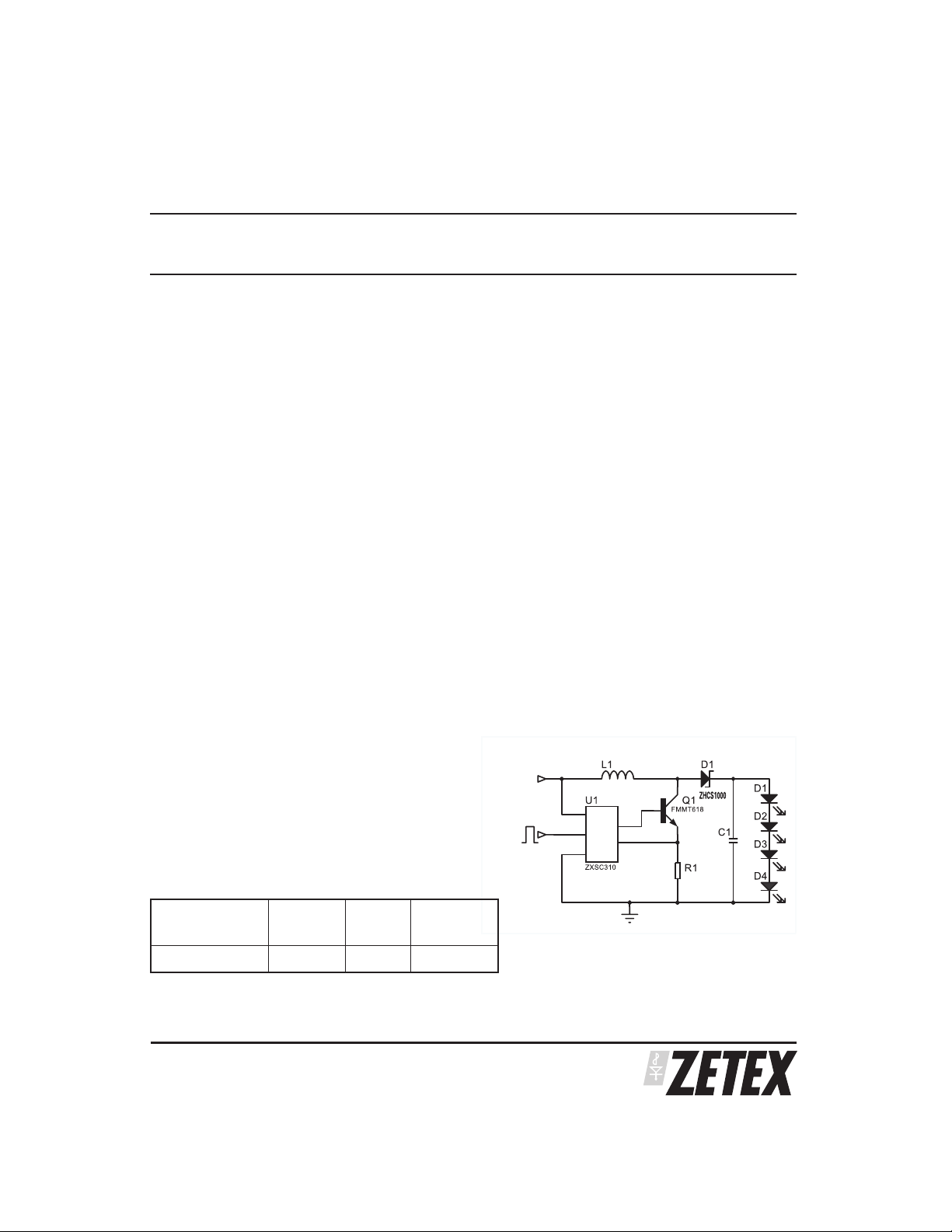
TYPICAL APPLICATIONS CIRCUIT
V
=3.3V/5V
IN
V
CC
V
DRIVE
S
TDN
I
SENSE
GND
DEVICE MARKINGS
·
C310
Package SOT23-5
ISSUE 2 - MARCH 2004
1
SEMICONDUCTORS
ZXSC310
ABSOLUTE MAXIMUM RATINGS:
Supply Voltage -0.3 to 10V
Maximum Voltage other pins -0.3 to V
Power Dissipation 450mW
Operating Temperature -40 to 85 °C
Storage Temperature -55 to 150°C
ELECTRICAL CHARACTERISTICS:
Test conditions unless otherwise stated: V
Symbol Parameter Conditions Min Typ Max Units
Efficiency
V
CC
V
CC(min)
I
Q
I
VDRIVE
I
CC
Recommended supply
voltage range
Minimum startup and
operating voltage
Quiescent current
Base drive current V
Supply current
1
2
3
CC
I
=-600µA,V
DRIVE
=-600µA, V
I
DRIVE
T
=-10°C3
AMB
V
EN =VCC
0V (standby)
V
EN =
DRIVE
V
DRIVE
=1.5V, T
(enabled)
= 0.7V, V
= 0.7V, V
+0.3V
CC
=25 C
AMB
0.8 8 V
DRIVE
DRIVE
=0.7V
=0.7V,
0.8
0.9
0.2
510mAµA
= 0V 1.5 3.5 mA
ISENSE
=0V 2 4 mA
ISENSE
94 %
0.92 V
V
VDRIVE(high)
V
VDRIVE(low)
V
STDN(high)
V
STDN(low)
I
STDN
V
ISENSE
(threshold)
T
CVISENSE
I
ISENSE
T
DRV
High level drive voltage V
Low level drive voltage V
ISENSE
ISENSE
=0V,I
VDRIVE
= 50mV, I
=-0.5mA V
= 5mA 0 0.2 V
VDRIVE
Device enabled 0.7 V
Device in standby mode 0.15 V
Enable input current -1 1 µA
Output current reference
voltage
I
voltage temp co.
SENSE
I
input current V
SENSE
2
= 0V 0 -30 -65 µA
ISENSE
Discharge Pulse Width 1.2 1.7 3.2 µs
OPERATING CONDITIONS
Symbol
F
OSC
1 Application dependent, see reference designs
2 These parameters guaranteed by Design and characteristics
3 Total supply current =I
4 Operating frequency is application circuit dependent. See applications section.
Parameter Conditions Min Typ Max Units
Recommended operating
frequency
Q+IVDRIVE
4
, see typical characteristics
CC
V
CC
-0.3
14 19 24 mV
0.4 %/°C
200 kHz
ISSUE 2 - MARCH 2004
V
SEMICONDUCTORS
2
ZXSC310
FMMT618
For the circuits described in the applications section
ZetexFMMT618 isthe recommendedpass transistor.
ELECTRICAL CHARACTERISTICS:
Test conditions unless otherwise stated: T
Symbol Parameter Conditions Min Typ Max Units
V
CE(sat)
V
(BR)CEO
5
Measured under pulse conditions. Pulse width=300µs. Duty cycle ⱕ2%
Collector-Emitter
Saturation Voltage
Collector-Emitter
Breakdown Voltage
5
5
IC=0.1A, IB=10mA
I
C
I
C
IC=10mA 20 27 V
ZHCS1000
The following indicates outline data for the device,
more detailed information can be found in the Zetex
surface mount products data book or on Zetex Web
page: www.zetex.com
=25 C
AMB
8
=1A, IB=10mA
=2.5A, IB=50mA
70
130
15
150
200
mV
For the maximum brightness circuit described in the
applications section Zetex ZHCS1000 is the
recommended Schottky diode.
The following indicates outline data for the ZHCS,
more detailed information can be found on Zetex Web
page: www.zetex.com
ELECTRICAL CHARACTERISTICS:
Test conditions unless otherwise stated: T
Symbol Parameter Conditions Min Typ Max Units
V
F
t
rr
I
R
Part
Number
BAT54 30 200 0.6 500 30 250 25 10 SOT23-6
ZHCS2000 40 2000 20 500 2000 1000 30 60 SOT23
ZHCS1000 40 1000 12 500 1000 100 30 25 SOT23
ZHCS750 40 750 12 540 750 100 30 25 SOT23
ZHCS500 40 500 6.75 550 500 40 30 20 SOT23
ZHCS400 40 400 6.75 500 400 40 30 20 SOT323
Forward voltage IF= 500mA
I
F
Reverse Recovery Time Switched from IF=500mA to
I
R
Measured at I
Reverse Current VR= 30V 50 100 µA
V
I
R
I
F
FSM
VFat IRat Capacitance
Max.VMax.mAMax.AMax.mVI
mA
AMB
=1A
=500mA.
Max.AV
F
=25 C
=50mA
R
R
V
= 25V, f = 1MHz
at V
R
Typ.
pF
400
500
12 ns
Package
SOT23
mV
ISSUE 2 - MARCH 2004
3
SEMICONDUCTORS
ZXSC310
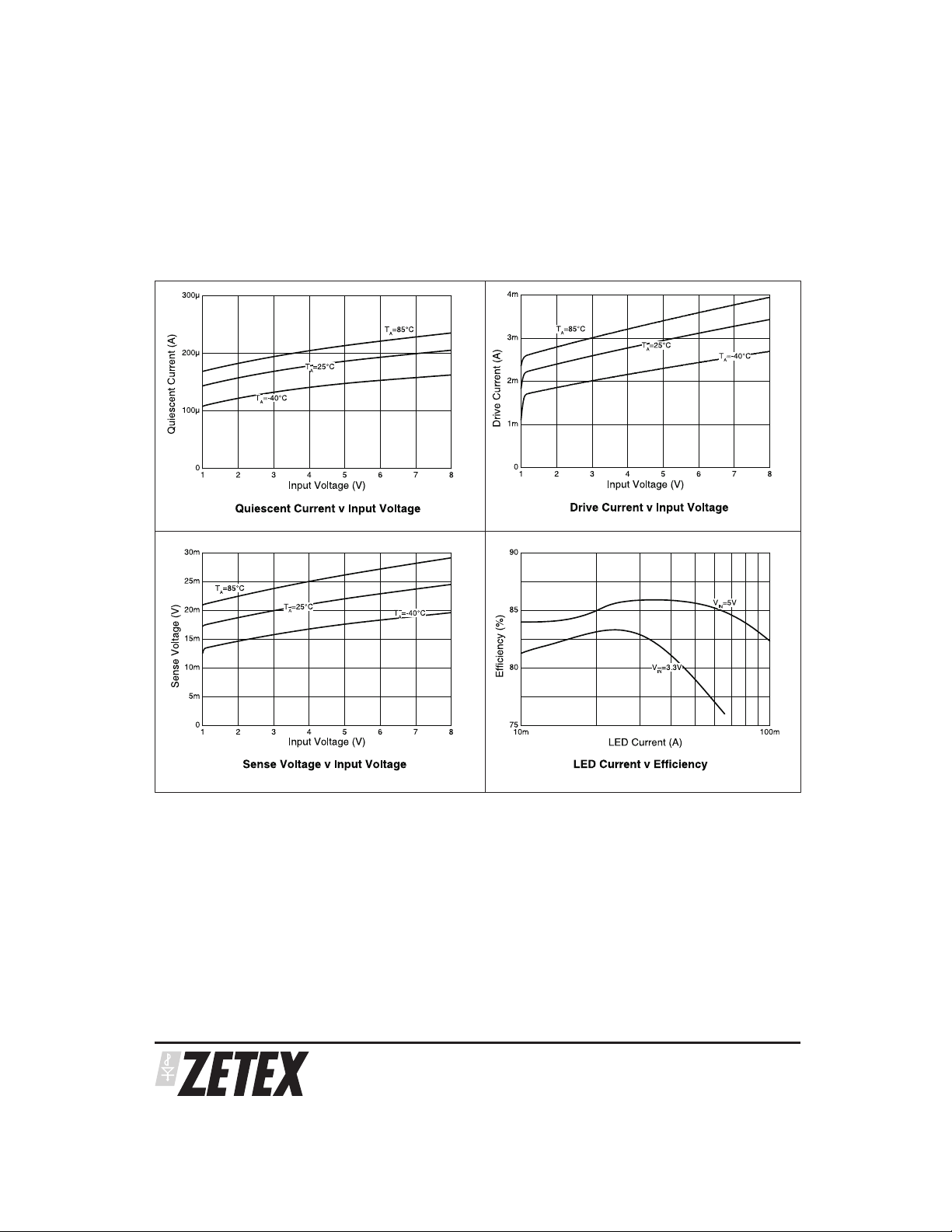
TYPICAL CHARACTERISTICS
SEMICONDUCTORS
ISSUE 2 - MARCH 2004
4
DEVICE DESCRIPTION
ZXSC310
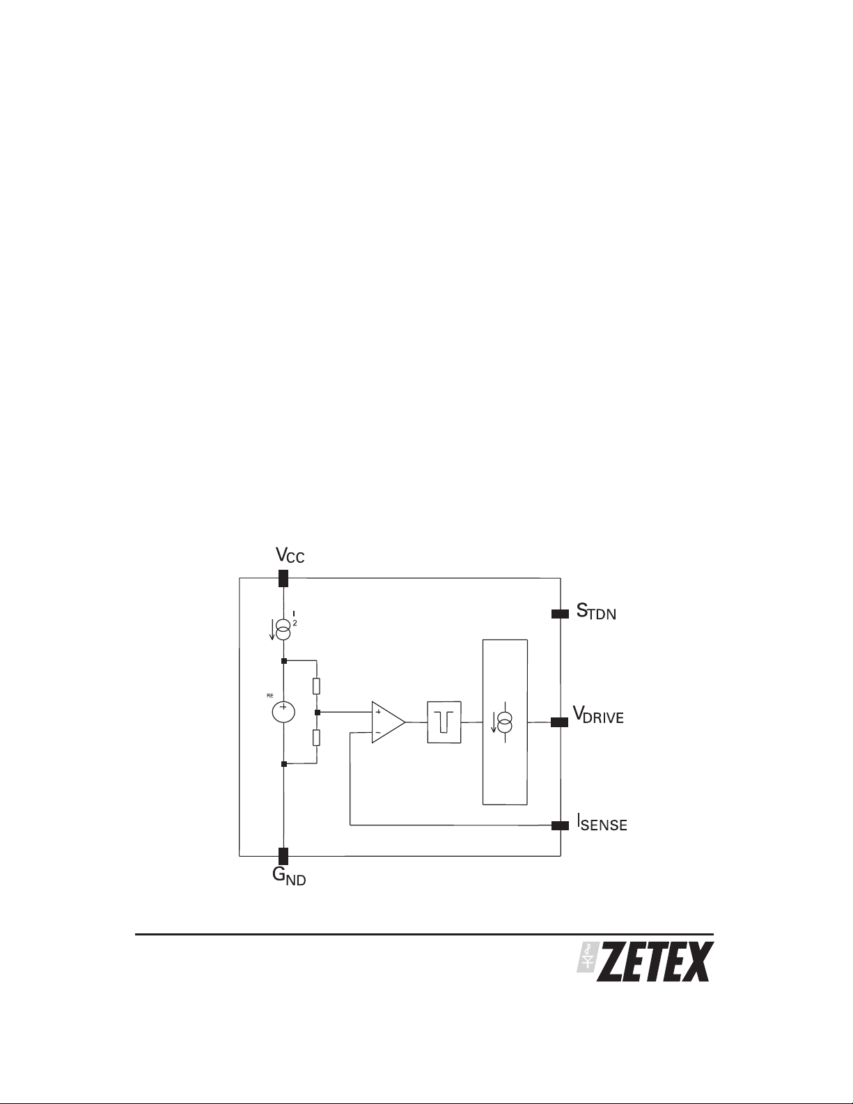
The ZXSC310 is PFM, controller IC which, when
combinedwith a high performance external transistor,
enables the production of a high efficiency boost
converter for LED driving applications. A block
diagram is shown for the ZXSC310 below.
The on chip comparator forces the driver circuit and
therefore the external switching transistor off if the
voltage at I
circuit and divider set this threshold.
The voltage at I
resistor connected in series with the emitter of the
switching transistor. A monostable following the
outputofthecomparatorforcestheturn-offtimeofthe
output stage to be typically 1.7us. This ensures that
there is sufficient time to discharge the inductor coil
before the next on period.
exceeds 19mV. An internal reference
SENSE
is taken from a current sense
SENSE
With every on pulse the switching transistor is kept on
until the voltage across the current-sense resistor
exceeds the threshold of the I
length, and therefore the switching frequency, is
determinedby theprogrammed peak current,the input
voltageand the inputto output voltagedifferential. See
applications section for details.
The driver circuit supplies the external switching
transistor with a fixed drive current. To maximise
efficiency the external transistor switched quickly,
typically being forced off within 30ns.
Drive
input. The on-pulse
SENSE
ZXSC310 Block Diagram
ISSUE 2 - MARCH 2004
R1
V
R2
5
I
SEMICONDUCTORS
 Loading...