

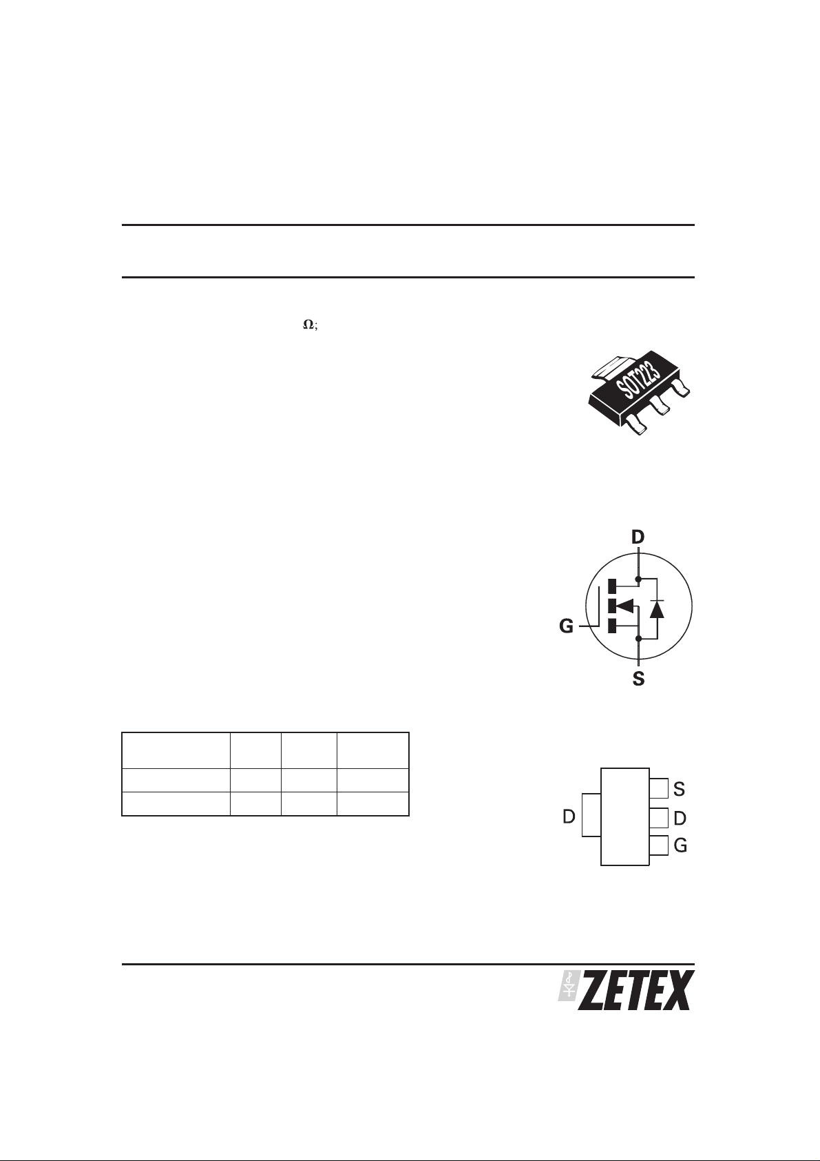
40V N-CHANNEL ENHANCEMENT MODE MOSFET
SUMMARY
V
(BR)DSS
DESCRIPTION
This new generation of TRENCH MOSFETs from Zetex utilizes a unique structure
that combines the benefits of low on-resistance with fast switching speed. This
makesthemidealforhighefficiency,lowvoltage,powermanagementapplications.
= 40V; R
= 0.05 ID= 7A
DS(ON)
ZXMN4A06G
FEATURES
Low on-resistance
•
Fast switching speed
•
Low threshold
•
Low gate drive
•
SOT223 package
•
APPLICATIONS
•
DC - DC Converters
•
Audio Output Stages
•
Relay and Solenoid driving
•
Motor control
ORDERING INFORMATION
DEVICE REEL
SIZE
ZXMN4A06GTA 7” 12mm 1000 units
ZXMN4A06GTC 13” 12mm 4000 units
TAPE
WIDTH
QUANTITY
PER REEL
DEVICE MARKING
•
ZXMN
4A06
SOT223
Top View
ISSUE 1 - MAY 2002
1
ZXMN4A06G
ABSOLUTE MAXIMUM RATINGS
PARAMETER SYMBOL LIMIT UNIT
Drain-Source Voltage V
Gate-Source Voltage V
Continuous Drain Current V
=10V; TA=25°C(b)
GS
V
=10V; TA=70°C(b)
GS
V
=10V; TA=25°C(a)
GS
Pulsed Drain Current (c) I
Continuous Source Current (Body Diode) (b) I
Pulsed Source Current (Body Diode)(c) I
Power Dissipation at T
Linear Derating Factor
Power Dissipation at T
Linear Derating Factor
=25°C (a)
A
=25°C (b)
A
Operating and Storage Temperature Range T
THERMAL RESISTANCE
I
D
DM
S
SM
P
P
DSS
GS
D
D
j:Tstg
40 V
20 V
7.0
5.6
5.0
22 A
5.4 A
22 A
2.0
16
mW/°C
3.9
31
mW/°C
-55 to +150 °C
A
W
W
PARAMETER SYMBOL VALUE UNIT
Junction to Ambient (a) R
Junction to Ambient (b) R
NOTES
(a) For a device surface mounted on 25mm x 25mm FR4 PCB with high coverage of single sided 1oz copper, in still air conditions
(b) For a device surface mounted on FR4 PCB measured at t⭐5 secs.
(c) Repetitive rating 25mm x 25mm FRA PCB, D=0.05 pulse width = 10s - pulse width limited by maximum junction temperature.
θJA
θJA
62.5 °C/W
32.2 °C/W
ISSUE 1 - MAY 2002
2
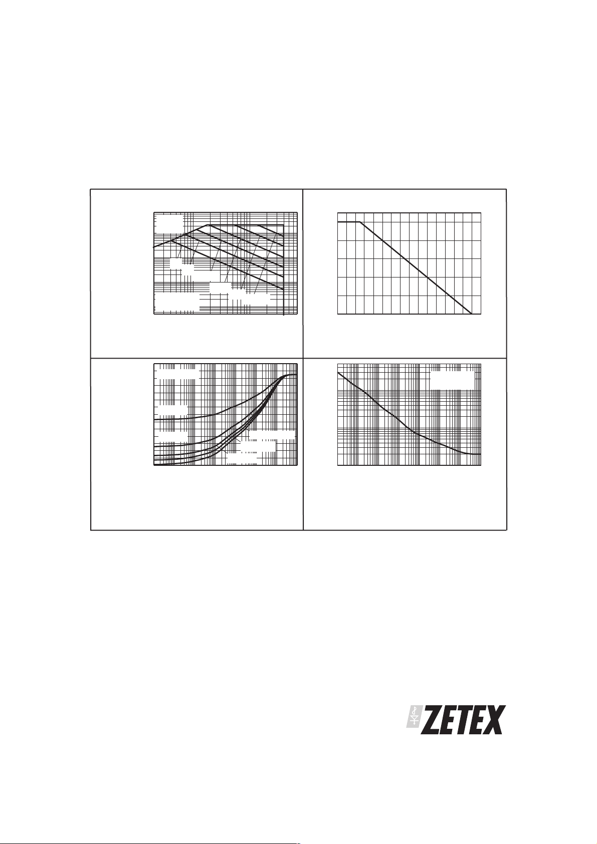
CHARACTERISTICS
ZXMN4A06G
R
DS(on)
Limi ted
10
1
DC
1s
100m
Single Pulse
Drain Current (A)
T
amb
10m
D
I
VDSDrain-Source Voltage (V)
100ms
10ms
1ms
= 25° C
110
100µs
Safe Operating Area
70
T
=25°C
amb
60
50
40
D= 0.5
30
20
D= 0.2
10
0
100µ 1m 10m100m 1 10 100 1k
Thermal Resistance (° C/W)
Transient Thermal Impedance
Pulse Width (s)
Single Pulse
D= 0.05
D= 0.1
2.0
1.6
1.2
0.8
0.4
0.0
0 20 40 60 80 100 120 140 160
Max Power Dissipation (W)
100
10
Maximum Power (W)
1
100µ 1m 10m100m 1 10 100 1k
Temperature (° C)
Derating Curve
Single Pulse
T
=25°C
amb
Pulse Width (s)
Pulse Power Dissipation
ISSUE 1 - MAY 2002
3
 Loading...