

查询SL1935供应商
Features
•
Single chip synthesised tuner solution for quadrature
down conversion, L-band to Zero IF.
•
DVB compliant, operating dynamic range -70 to
-20dBm.
•
Compatible with DSS and DVB variable symbol rate
applications.
•
Selectable baseband path, programmable through
2
I
C bus.
•
Excellent quadrature balance up to 30MHz
baseband
•
Excellent immunity to spurious second harmonic
(RF and LO) mixing effects.
•
Low oscillator phase noise and reradiation.
•
High output referred linearity for low distortion and
multi channel application.
•
Integral fast mode compliant I
frequency synthesiser, designed for high comparison
frequencies and low phase noise performance.
•
Buffered crystal output for clocking QPSK
demodulator.
•
ESD protection (Normal ESD handling procedures
should be observed).
Applications
••Satellite receiver systems.
Data communications systems.
2
C bus controlled PLL
SL1935
Single Chip Synthesized Zero IF Tuner
April 2004
Ordering Information
SL1935D/KG/NP1P (Tubes) 36 pin SSOP
SL1935D/KG/NP1Q (Tape and Reel) 36 pin SSOP
Description
The SL1935 is a complete single chip bus controlled
Zero IF tuner and operates from 950 to 2150MHz. It
includes an on-board low phase noise PLL frequency
synthesiser and low noise LNA/AGC. The SL1935 is
intended primarily for application in digital satellite Network
Interface Modules and performs the complete tuner
function.
The device contains all elements necessary, with the
exception of local oscillator tuning network and crystal
reference, to produce a high performance I(n-phase) &
Q(uadrature) downconversion tuner function. Due to the
high signal handling design the device does not require
any front end tracking filters.
The SL1935 includes selectable baseband signal paths,
allowing application with two externally definable filter
bandwidths, facilitating application in variable symbol
rate and simulcast systems. The SL1935 is optimised to
interface with the VP310 (ADC/QPSK/FEC) Satellite
Channel Decoder, available from Zarlink Semiconductor
and offers a full front end solution.
2
I
C
XTALCAP
XTAL
SDA
SCL
BUFREF
VCCD
VCC
RF
RFB
VCC
IFIA
IFIB
VCC
OFIA
OFIB
VEE
IOUT
ADD
Zarlink, ZL and the Zarlink Semiconductor logo are trademarks of Zarlink Semiconductor Inc.
Copyright 2003 - 2004, Zarlink Semiconductor Inc. All Rights Reserved.
1
18 19
Figure 1.
Zarlink Semiconductor Inc.
Pin connections
1
36
PUMP
DRIVE
PORT P0
VEE
TANKS
TANKSB
VEE
TANKV
TANKVB
VEE
IFQA
IFQB
VCC
OFQA
OFQB
VEE
QOUT
AGCCONT
SL1935
RFB
9
RF
8
AGCCONT
19
VCC
7,10,13,24
VCCD
VEE
16,21,27,30,33
TANKV 29
TANKVB 28
TANKS 32
TANKSB 31
SDA 3
SCL 4
ADD 18
XTAL 2
XTALCAP 1
6
RF Section
RF section
PLL section
VCOV
VCOS
PLL Section
REF
OSC
Divide
by 2
VS
AG C
Sender
90deg
Frequency
Agile
Phase
Splitter
15 bit
Programmab le
BS
I2C Bus Interface
Divider
Reference
Divider
23 OFQA
22 OFQB
26 IFQA
25 IFQB
20 QOUT
BS
17 IOUT
11 IFIA
12 IFIB
0deg
Fpd
Charge
Pump
Fpd/2
Fcomp
14 OFIA
15 OFIB
36 PUMP
35 DRIVE
34 PORT P0
5 BUFREF
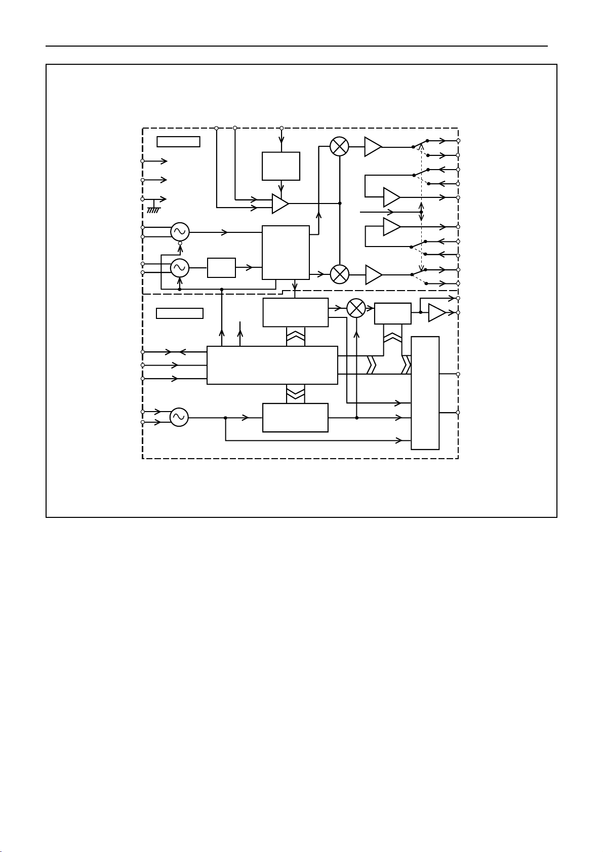
Figure 2. Block diagram
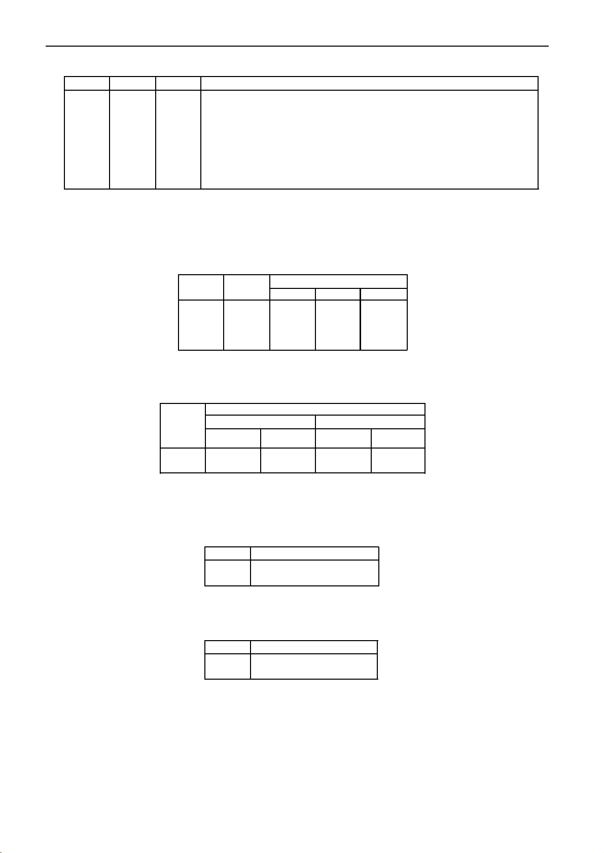
2

Table 1. Quick Reference Data
SL1935
Characteristic
Operating range
Input dynamic range
VSWR with input match
Input NF
@ -70dBm operating sensitivity
@ -60dBm operating sensitivity
IPIP3 @ -20dBm operating sensitivity
IPIP2@ -20dBm operating sensitivity
IPP1dB@ -20dBm operating sensitivity
Baseband output limit voltage
Gain match up to 22MHz
Phase match up to 22MHz
Gain flatness up to 30MHz
Local oscillator phase noise
SSB at 10kHz offset
In band LO reradiation from RF input
LO second harmonic interference level at input level of
-20dBm per carrier
LNA second harmonic interference level at input level
of -25dBm per carrier
PLL maximum comparison frequency
PLL phase noise at phase detector
`
Note: 6dB interstage filter loss assumed in external base band paths.
dBm assumes 75Ω characteristic impedance.
`
Value Units
950 to 2150
-75 to -15
10
10
15
+5
+20
-5
2.0
0.2
0.7
1
-80
<-70
-55
-35
4
-152
MHz
dBm
dB
dB
dB
dBm
dBm
dBm
V
dB
deg
dB
dBc/Hz
dBm
dBc
dBc
MHz
dBc/Hz
Functional Description
General
The SL1935 is a complete wideband direct conversion
tuner incorporating an on board frequency synthesiser
and LNA/AGC, optimised for application in digital satellite
receiver systems. The device offers a highly integrated
solution to a satellite tuner function, incorporating an I2C
bus interface controller, a low phase noise PLL frequency
synthesiser and all tuner analogue functionality. The
analogue blocks include the reference oscillator,
consisting of two independent oscillators, a phase splitter,
RF preamplifier with AGC facility, channel mixers and
baseband amplifiers incorporating two selectable
baseband paths, allowing for two externally definable
bandwidths. In this application two varactor tuned tanks,
a reference crystal and baseband filtering components
are required to complete the tuner system.
A buffered crystal frequency output is available to clock
the QPSK demodulator and powers up in the active
state.
The I2C bus interface controls the frequency synthesiser,
the local oscillator, the baseband path selection, the
buffered reference frequency output and an external
switching port.
Figure 2 shows the device block diagram and pin
allocations are shown in Figure 1.
Quadrature Downconverter Section
In normal application the tuner IF frequency of typically
950 to 2150MHz is fed direct to the SL1935 RF input
through an appropriate impedance match (Fig.16) and
LNB switching. The input stage is optimised for both NF
and signal handling.
The signal handling of the front end is designed to offer
immunity to input composite overload without the
requirement of a tracking filter. RF input impedance is
shown in Fig.3.
The RF input amplifier feeds an AGC stage and provides
system gain control. The system AGC gain range will
guarantee an operating dynamic range of -70 to -20dBm.
The AGC is controlled by the AGC sender and is optimised
for S/N and S/I performance across the full dynamic
range. Details of the AGC characteristics, variations in
IIP3, IIP2, P1dB and NF are illustrated in Figs.4, 5, 6, 7,
and 8 respectively.
The required I and Q local oscillator frequencies for
quadrature downconversion are generated by the onboard reference oscillators designated ‘VCOS’ and
‘VCOV’. VCOS operates nominally from 1900 to 3000MHz
and is then divided by two to provide 950 to 1500MHz.
VCOV operates nominally from 1400 to 2200MHz. Only
the oscillator selected via bit VS in the I
transmission is powered.
2
C data
3

SL1935
Quadrature Downconverter Section - continued
The oscillators share a common varactor line drive and
both require an external varactor tuned resonator
optimised for low phase noise performance. The
recommended application circuit for the local oscillators
is detailed in Fig.9 and the typical phase noise
performance is detailed in Fig.10. The local oscillator
frequency is coupled internally to the PLL frequency
synthesiser programmable divider input.
The mixer outputs are coupled to the baseband buffer
amplifiers, providing for one of two selectable baseband
outputs in each channel. The required output is selected
by bit BS in the I2C bus transmission (Table 6). These
outputs are fed off chip via ports ‘OPIA’ and ‘OPIB’
(‘OPQA’ and ‘OPQB’), then back on chip through ports
‘IPIA’ and ‘IPIB’ (‘IPQA’ and ‘IPQB’), allowing for the
insertion of two independent user definable filter
bandwidths. Each output provides a low impedance
drive (Fig.11) and each input provides a high impedance
load . An example filter for 30MS/s is detailed in Fig.13.
Both path gains are nominally equal. NB 6dB insertion
loss is assumed in each channel, however a different pot
down ratio may be applied.
Each baseband path is then multiplexed to the final
baseband amplifier stage, providing further gain and a
low impedance output drive. The nominal output load
test condition is detailed in Fig.14.
PLL Frequency Synthesiser Section
The PLL frequency synthesiser section contains all the
elements necessary, with the exception of a reference
frequency source and a loop filter to control the selected
oscillator to produce a complete PLL frequency
synthesised source. The device, produced using high
speed logic, allows for operation with a high comparison
frequency and enables the generation of a loop with
excellent phase noise performance.
The LO signal from the selected oscillator drives from the
phase splitter into an internal preamplifier, providing gain
and reverse isolation from the divider signals. The output
of the preamplifier interfaces directly with the 15-bit fully
programmable divider. The programmable divider has
MN+A architecture, the dual modulus prescaler is 16/17,
the A counter is 4-bits and the M counter is 11-bits.
The output of the programmable divider is fed to the
phase comparator and compared in both phase and
frequency domains to the comparison frequency. This
frequency is derived from either the on board crystal
controlled oscillator or from an external reference source.
In both cases the reference frequency is divided down to
the comparison frequency by the reference divider,
programmable into 1 of 29 ratios and detailed in Table 3.
The typical application for the crystal oscillator is shown
in Fig.15.
The output of the phase detector feeds a charge pump
and a loop amplifier. When used with an external loop
filter and a high voltage transistor it integrates the current
pulses into the varactor line voltage used to control the
selected oscillator.
The programmable divider output Fpd divided by two
and the reference divider output Fcomp are switched to
port P0 by programming the device into test mode. Test
modes are detailed in Table 4.
The crystal reference frequency can be switched to the
BUFREF output by bit RE as detailed in Table 7.
Programming
The SL1935 is controlled by an I2C data bus and is
compatible with both standard and fast mode formats.
Data and Clock are fed on the SDA and SCL lines
respectively as defined by the I2C bus format. The
device can either accept data (write mode) or send data
(read mode). The LSB of the address byte (R/W) sets the
device into write mode if it is low and read mode if it is
high. Tables 9a and 9b detail the format of the data. The
SL1935 may be programmed to respond to several
addresses and enables the use of more than one device
in an I
address is selected by applying a voltage to the ‘ADD’
input. When the device receives a valid address byte, it
pulls the SDA line low during the acknowledge period
and during following acknowledge periods after further
data bytes are received. When the device is
programmed into read mode, the controller accepting
the data must pull the SDA line low during all status byte
acknowledge periods to read another status byte. If the
controller fails to pull the SDA line low during this period,
the device generates an internal ‘STOP’ condition which
inhibits further reading.
Write mode
Bytes 2 and 3 contain frequency information bits 2
inclusive (Table 9). Byte 4 controls the synthesiser
reference divider ratio (Table 3) and the charge pump
setting (Table 5). Byte 5 controls test modes (Table 4),
baseband filter path select BS (Table 6), local oscillator
select VS (Table 8), buffered crystal reference output
select RE (Table 7) and the output port P0.
After reception and acknowledgment of a correct
address (byte 1), the first bit of the following byte
determines whether the byte is interpreted as byte 2 or
4, a logic ‘0’ indicates byte 2 and a logic ‘1’ indicates byte
4. Having interpreted this byte as either byte 2 or 4, the
following byte will be interpreted as byte 3 or 5
respectively. After receiving two complete data bytes,
additional data bytes may be entered and byte
interpretation follows the same procedure without readdressing the device. The procedure continues until a
‘STOP’
2
C bus system. Table 9c details the how the
14
to 2
condition is received.
0
4

SL1935
The STOP condition can be generated after any data
byte, if however it occurs during a byte transmission, the
previous byte data is retained. To facilitate smooth fine
tuning, the frequency data bytes are only accepted by
the device after all 15 bits of frequency data have been
received, or after the generation of a STOP condition.
Read mode
When the device is in read mode, the status byte read
from the device takes the form shown in Table 9b.
Table 2. Programmable Features
Programmable features
Synthesiser programmable divider
Reference programmable divider
Baseband filter path select
Local oscillator select
Charge pump current
Test mode
General purpose port, P0
Buffered crystal reference output,
BUFREF
Function as described above
Function as described above.
Function as described above.
Function as described above.
The charge pump current can be programmed by bits C1 & C0 (Table 5).
The test modes are defined by bits T2 - T0 as described in Table 4.
The general purpose port can be programmed by bit P0;
Logic ‘1’ = on
Logic ‘0’ = off (high impedance)
The buffered crystal reference frequency can be switched to the BUFREF
output by bit RE as described in Table 7. The BUFREF output defaults to
the ‘ON’ condition at device power up.
Bit 1 (POR) is the power-on reset indicator, and this is set
to a logic ‘1’ if the Vccd supply to the device has dropped
below 3V (at 25oC), e.g. when the device is initially turned
ON. The POR is reset to ‘0’ when the read sequence is
terminated by a STOP command. When POR is set high
this indicates that the programmed information may
have been corrupted and the device reset to the power
up condition.
Bit 2 (FL) indicates whether the synthesiser is phase
locked, a logic ‘1’ is present if the device is locked, and
a logic ‘0’ if the device is unlocked.
Function
The typical key performance data at Vcc = 5V and +25oC ambient are detailed in Table 1.
Table 3. Reference division ratios
R4
0
0
0
0
0
0
0
0
0
0
0
0
0
0
0
0
1
1
1
1
1
1
1
1
1
1
1
1
1
1
1
1
R3
0
0
0
0
0
0
0
0
1
1
1
1
1
1
1
1
0
0
0
0
0
0
0
0
1
1
1
1
1
1
1
1
R2
R1
0
0
0
0
1
1
1
1
0
0
0
0
1
1
1
1
0
0
0
0
1
1
1
1
0
0
0
0
1
1
1
1
0
0
1
1
0
0
1
1
0
0
1
1
0
0
1
1
0
0
1
1
0
0
1
1
0
0
1
1
0
0
1
1
R0
0
1
0
1
0
1
0
1
0
1
0
1
0
1
0
1
0
1
0
1
0
1
0
1
0
1
0
1
0
1
0
1
Ratio
2
4
8
16
32
64
128
256
Illegal state
5
10
20
40
80
160
320
Illegal state
6
12
24
48
96
192
384
Illegal state
7
14
28
56
112
224
448
5
SL1935
Table 4. Test modes
T2
0
0
0
0
1
1
1
1
Note: * Clocks need to be present on crystal and RF inputs to enable charge pump test modes and to
toggle status byte bit FL.
T1
0
0
1
1
0
0
1
1
T0
0
1
0
1
0
1
0
1
Test mode description
Normal operation
Charge pump sink* (status byte FL set to logic '0')
Charge pump source* (status byte FL set to logic '0')
Charge pump disabled* (status byte FL set to logic '1')
Normal operation and port P0 = Fpd/2
Charge pump sink* (status byte FL set to logic '0'. Port P0 = Fcomp)
Charge pump source* (status byte FL set to logic '0'. Port P0 = Fcomp)
Charge pump disabled* (status byte FL set to logic '1'. Port P0 = Fcomp)
Table 5. Charge pump current
C0C1
0
0
1
1
0
1
0
1
min
+-116
+-247
+-517
+-1087
Current in µA
typ
+-155
+-330
+-690
+-1450
max
+-194
+-412
+-862
+-1812
Table 6. Baseband path select
BS
0
1
Path Selected
I Channel Q Channel
Filter drive
output
OFIB
OFIA
Baseband
amp input
IFIB
IFIA
Filter drive
output
OFQB
OFQA
Baseband
Table 7. Buffered crystal
reference output select
RE
0
1
BUFREF output
Disabled, high impedance
Enabled
Table 8. Local oscillator select
VS
Local oscillator selected
0
1
VCOV
VCOS
amp input
IFQB
IFQA
6
Table 9a. Write data format (MSB is transmitted first)
Address
Programmable
divider
Programmable
divider
Control data
Control data
Table 9b. Read data format (MSB is transmitted first)
Address
Status Byte
MSB
2
2
C0
T0
0
13
2
5
2
R4
VS
1
0
2
1
T2
1
14
2
7
6
2
C1
T1
MSB
1
POR1FL
0
0
0
0
Table 9c. Address selection
Note:
MA1
0
0
1
1
Programmed by connecting a 30kΩ resistor between pin and Vcc
*
MA0
0
1
0
1
0
12
4
0
2
2
R3
BS
0
0
11
3
MA1
2
2
R2
MA0
10
2
9
2
1
2
R1
0
RE
MA10MA0
0
Address input voltage level
0 - 0.1 Vcc
Open circuit
0.4 Vcc - 0.6 Vcc*
0.9 Vcc - Vcc
LSB
0
2
2
R0
P0
LSB
1
0
SL1935
A
8
0
Byte 1
A
Byte 2
A
Byte 3
A
Byte 4
A
Byte 5
AAByte 1
Byte 2
Key to Tables 9a to 9c
A ......................................... Acknowledge bit
MA1, MA0 ........................... Variable address bits (Table 9c)
14
2
C1 to C0 .............................. Charge pump current select (Table 5)
R4 to R0 .............................. Reference division ratio select (Table 3)
T2 to T0 .............................. Test modes control bits (Table 4)
BS ....................................... Baseband path select (Table 6)
VS ....................................... Local oscillator select (Table 8)
RE ....................................... Buffered crystal reference output enable (Table 7)
P0 ....................................... P0 port output state
POR .................................... Power on reset indicator
FL ........................................ Phase lock flag
+j0.2
0
—j0.2
—j0.5
START 950MHz
Normalised to 75 Ω
to 2 0................................ Programmable division ratio control bits
+j1
+j0.5
0.50.2
1
X
X
X
4
3
2
—j1
+j2
+j5
2
5
Marker
X
X
1
—j5
—j2
STOP 2150MHz
1
2
3
4
Freq (MHz)
950
1400
1600
2150
Z real Ω
64
40
32
23
Z imag Ω
-100
-75
-65
-45
Figure
RF input impedance (typical)
3.
7

SL1935
90
80
70
70dB minimum, AGC < 0.75V
60
50
40
30
20
6dB interstage filter loss
System gain (dB) assuming
10
0
0 0.5 1 1.5 2 2.5 3 3.5 4 4.5 5
20dB maximum, AGC > 4.25V
AGCCONT Voltage (V)
Figure 4. AGC characteristic (typical)
120
110
100
90
80
70
System input referred IP3 (dBuV)
60
20 25 30 35 40 45 50 55 60 65 70
System gain (dB) assuming 6dB interstage filter loss
Figure 5. Variation in IIP3 with system gain (typical)
170
160
150
140
130
120
110
System input referred IP2 (dBuV)
100
8
Baseband dominated IP2
LNA dominated IP2
20 25 30 35 40 45 50 55 60 65 70
Figure 6. Variation in IIP2 with system gain (typical)
System gain (dB) assuming 6dB interstage filter loss

110
105
100
95
90
85
80
75
70
65
Converter input referred P1dB (dBuV)
60
-10
-5 0 5
Converter gain seting (dB) from RF inputs OFIA/OFQA or OFIB/OFQB outputs
SL1935
10
15 20
25
30 35 40 45
Figure 7. Variation in P1dB with converter gain (typical)
60
50
40
30
20
Noise figure (dB)
10
0
20 25 30 35 40 45 50 55 60 65 70 75 80
System gain (dB) assuming 6dB inter stage filter loss
Figure 8. Variation in NF with system gain (typical)
BB837
1kΩ
4mm STRIPLINE
2kΩ
6
Tanks
"vcos"
Vcnt
1kΩ
BB837
BB831
BB831
4mm STRIPLINE
10mm STRIPLINE
2kΩ
10mm STRIPLINE
7
9
10
Tanksb
Tankv
"vcov"
Tankvb
Figure 9. Local oscillator application circuit
NOTE:
Stripline width = 0.44mm
(dimensions are approximate)
9

SL1935
v
900 1000 1100 1200 1300 1400 1500 1600 1700 1800 1900 2000 2100
-70
-72
-74
-76
-78
-80
-82
-84
Phase noise @ 10kHz offset (dBc/Hz)
-86
-88
-90
vcos enabled
Conditions:
Loop filter as per standard application shown in Figure 21
Charge pump = 130uA
Fcomp = 65.5kHz or 125kHz
LO Frequency (MHz)
cov enabled
Figure 10. Local oscillator phase noise variation with frequency (typical)
+j1
+j0.2
—j0.2
+j0.5
3
x
x
2
x
1
0.50.2 10
x
2
+j2
4
+j5
5
—j5
Marker
1
2
3
4
Freq (MHz)
1
10
20
30
Z real Ω
17
18
22
33
Z imag Ω
0
19
38
60
START 1MHz
Normalised to 50Ω
Figure 11. Converter output impedance; OFIA, OFIB, OFQA, OFQB (typical)
+j0.2
—j0.2
START 100kHz
Normalised to 50Ω
—j0.5
0.2
+j0.5
—j0.5
—j1
+j1
X
4
X
3
0.5 10
X
2
X
1
—j1
—j2
STOP 30MHz
+j2
+j5
Marker
2
5
X
—j5
—j2
Freq (MHz) Z real Ω
1
2
3
4
0.1
10
20
30
STOP 30MHz
Figure 12. Baseband output impedance; IOUT, QOUT (typical)
9.5
10.0
10.6
12.6
Z imag Ω
-2.0
1.3
3.3
5.5
10

SL1935
OFIA/OFIB
OFQA/OFQB
Figure 13. Example baseband interstage filter for 30MS/s
100nF
220nF
1k Ω
100 Ω
1k Ω
1k Ω
100nF
IFIA/IFIB
IFQA/IFQB
3.9pF
15pF
Figure 14. Nominal baseband output load test condition
1 XTALCAP
150pF
82pF
4MHz
2 XTAL
Figure 15. Crystal oscillator application (typical)
11

SL1935
1pF
33 Ω
RFIN
2.2pF
100pF
100pF
8
RF
9
RFB
SL1935
Figure 16. Input matching network
Table 10. Electrical Characteristics
Test conditions (unless otherwise stated); Tamb = -20o to +80oC, Vee= 0V, Vcc =Vccd = 5V+-5%.
These characteristics are guaranteed by either production test or design. They apply within the specified ambient
temperature and supply voltage unless otherwise stated.
Characteristic
Supply current
RF input operating frequency
SYSTEM
System noise figure DSB
Variation in system NF with gain
adjust
System input referred IP2
Variation in system input referred
IP2 with operating sensitivity
System input referred IP3
Variation in system input referred
IP3 with operating sensitivity
Pin
6,7,10
13,24
8,9 950
Value
Min Max
Typ
130
175
2150
10
15
12
17
-1
121
140
112
Units
mA
MHz
dB
dB
dB/dB
dBµV
dBµV
Conditions
VCCD (PLL) and VCC
All system specification items should
be read in conjunction with Note 2
At -70dBm operating sensitivity
At -60dBm operating sensitivity
Above –60dBm operating sensitivity,
(Fig.7)
At –20dBm operating sensitivity, see
Notes 3 and 4
(Fig.6)
At -20dBm operating sensitivity,
see Note 5
(Fig.5)
Continued
12

SL1935
Table 10. Electrical Characteristics
Characteristic
System dynamic range
System gain roll off
System gain variation with
temperature
System I Q gain match
System I Q phase balance
System I and Q channel in band
ripple
System baseband path gain
match
LO second harmonic interference
level
LNA second harmonic
interference level
Synthesiser and other spurii on I
and Q outputs
In band leakage to RF input
CONVERTER
Converter input impedance
Converter input return loss
System input referred P1dB
Converter output impedance, OFIA,
OFIB, OPQA and OPQB.
Converter output leakage to
unselected output, OFIA, OFIB,
OPQA and OPQB.
Oscillator VCOS operating range
Oscillator VCOV operating range
Local oscillator SSB phase noise
AGCONT input current
Pin
17,20
17,20
17,20
17,20
8,9
8,9
8,9
14,15
22,23
31,32
28,29
19 -150 150
(Continued)
Value
Min Max
-70
-1
-3
-1
102
1900
1450
Typ
3
2
-50
-35
-60
75
8
25
-26
-78
-20
+1
+3
1
+1
76
50
3000
2150
Units Conditions
Note 6
dBm
dBm
deg
dBc
dBc
dBµV
dBm
dBµV
dBc
MHz
MHz
dBc/Hz
AGCCONT = 0.75V
AGCCONT = 4.25V
dB
Within RF band 950-2150MHz
dB
-20˚C to +80˚C
dB
Interstage filter (Fig.13)
Interstage filter (Fig.13)
dB
Interstage filter (Fig.13)
dB
Note 8.
Note 9.
Within 0-100MHz band under all gain
settings, RF input set to deliver
108dBµV on output
Within RF band 950-2150MHz.
Note 11.
Ω
dB
With input matching (Fig.16)
Converter gain =-5dBm (to OFIA/
OPQA, OFIB/OPQB outputs. Fig.7)
Ω
0.1 to 30MHz (Fig.11)
Relative to selected output
Giving LO = 950 to 1500MHz
(Application as in Fig.9)
(Application as in Fig.9)
@10kHz offset, PLL loop bw < 1kHz
Application is measured at baseband
output frequency of 10MHz (Fig.10).
µA
BASEBAND AMPLIFIERS
Baseband input impedance, IFIA,
IFIB, IFQA And IFQB.
Resistance
Capacitance
Baseband unselected input
leakage to output
Baseband amplifier output
impedance
Baseband output limiting
Baseband bandwidth 1dB
Baseband output roll-off
11,12
25,26
17,20
17,20
17,20
17,20
10
40
6
2.0
5
-40
20
kΩ
pF
dBc
Ω
Vp-p
MHz
dB/oct
The baseband inputs must be
externally ac coupled
0.1- 30MHz bandwidth
Relative to selected input.
Level at hard clipping (load as Fig.14)
(Load as Fig.14)
Above 3dB point, no load
Continued
13

SL1935
Table 10. Electrical Characteristics
Characteristic
SYNTHESISER
SDA,SCL
Input high voltage
Input low voltage
Input high current
Input low current
Leakage current
Hysterysis
SDA output voltage
SCL clock rate
Charge pump output current
Charge pump output leakage
Charge pump drive output current
Crystal frequency
Recommended crystal series
resistance
External reference input frequency
External reference drive level
Phase detector comparison
frequency
Equivalent phase noise at phase
detector
Local oscillator programmable
divider division ratio
Reference division ratio
Output port P0
Sink current
Leakage current
BUFREF output
Output amplitude
Output impedance
Address select
Input high curent
Input low current
Pin
3,4
3
4
36
36
35
1,2
2
2
34
5
18
(Continued)
Value
Min Max
Typ
3
0
-10
0.4
+-3
0.5
2
10
2
0.2
-152
240
2
0.25
0.35
250
5.5
1.5
10
10
0.4
0.6
400
+-10
20
200
20
0.5
4
32767
10
0.45
1
-0.5
Units Conditions
2
I
C 'fast mode' compliant
V
V
µA
Input voltage = Vcc
µA
Input voltage = Vee
Vcc = Vee = 0V
µA
V
Isink = 3mA
V
Isink = 6mA
V
kHz
Vpin36 = 2V. (Table 5)
Vpin36 = 2V
nA
Vpin35 = 0.7V
mA
MHz
MHz
(Fig.15 for application)
4MHz parallel resonant crystal
Ω
Sinewave coupled via 10nF blocking
capacitor
Vpp
Sinewave coupled via 10nF blocking
capacitor
MHz
dBc/Hz
SSB within loop bandwidth, all
comparison frequencies
(Table 3)
(Note 7)
mA
Vport = 0.7
µA
Vport = Vcc
AC coupled. (Note 10.)
Vpp
Enabled by bit RE = 1 and default
Ω
state on power-up.
(Table 9c)
mA
Vin = Vcc
mA
Vin = Vee
Notes to Table 10
All power levels are referred to 75Ω, and 0dBm = 109dBµV.
1.
System specifications refer to total cascaded system of converter/AGC stage and baseband amplifier stagewith nominal
2.
6dB pad as interstage filter and load impedance as detailed in Figure 14.
Baseband dominated IP2. AGC set for 20dB system gain with two tones for intermodulation test at fc+146and
3.
fc+155MHz at 100dBµV generating output intermodulation spur at 9MHz. 30MHz 3dB bandwidthinterstage filter included.
LNA dominated IP2. AGC set for 20dB system gain with two tones for intermodulation test at fc+146 and2*fc+155 MHz at
4.
100dBµV generating output intermodulation spur at 9MHz. 30MHz 3dB bandwidthinterstage filter included.
AGC set for 20dB system gain with two tones for intermodulation test at fc+110 and fc+211MHz at 100dBµVgenerating
5.
output intermodulation spur at 9MHz. 30MHz 3dB bandwidth interstage filter included.
Dynamic range assuming termination as detailed in Figure 14, and including 6 dB interstage filter insertion loss,
6.
delivering 700mVp-p at baseband outputs (pins 17,20). AGC monotonic from Vee to Vcc (Fig.4).
Port powers up in high impedance state.
7.
The level of 2.01GHz downconverted to baseband relative to 1.01GHz with the oscillator tuned to 1GHz,measured with
8.
no input pre-filtering.
The level of second harmonic of 1.01GHz input at –25dBm downconverted to baseband relative to 2.01GHz at–40 dBm
9.
with the oscillator tuned to 2GHz, measured with no input pre-filtering.
If the BUFREF output is not used it should be left open circuit or connected to Vccd, and disabled by settingRE = ‘0’.
10.
This parameter is very application dependant. With good RF isolation <-60dBm can be achieved.
11.
14

RF
RFB
SL1935
V
CC
V
8
30K
9
AGCCONT
19
REF
5K
V
REF2
1K 1K
TANK
TANKB
Oscillator inputs
RF inputs
(pins 28, 29 and 31, 32)
AGC input
OFIA
OFIB
OFQA
OFQB
Converter outputs
(pins 14, 15, 22 and 23)
IFIA
IFIB
IFQA
IFQB
Baseband amplifier inputs
(pins 11, 12, 25 and 23)
Figure 17. Input and output interface circuits (RF section)
BIAS
IOUT
and
QOUT
Baseband outputs (pins 17 and 20)
15

SL1935
XTAL
XTALCAP
V
ccd
V
ccd
36
PUMP
2
1
300
35
DRIVE
SCL/SDA
]
On SDA only
SDA/SCL (pins 3 and 4)
Reference oscillator
47K
]
ACK
P0
34
Loop amplifier
V
ccd
60K
3K
18
ADD
20K
ENABLE/
DISABLE
ADD input
V
ccd
5
V
BUFREF
ccd
16
Output port
BUFREF output
Figure 18. Input and output interface circuits (PLL section)

SL1935
Table 11. Absolute Maximum Ratings
Characteristic
Supply voltage
SD
A, SCL DC offsets
All I/O port DC offsets
Por
t P0 current
Storage temperature
J
unction temperature
Pac
kage thermal resistance,
(All voltages referred to Vee at 0V and Vcc = Vccd)
Min Max
-0.3
-0.3
-0.3
Vcc+0.3
-55
chip to case
Pac
kage thermal resistance,
chip to ambient
Po
wer consumption at 5.25V
ESD protection
3.5
SL1935 Demo Board
The demo board contains an SL1935 I2C bus controlled
Zero IF tuner IC, plus all components necessary to
demonstrate operation of the SL1935. The schematic
and PCB layout of the board are shown in Figures 19, 20
and 21.
Supplies
The board must be provided with the following supplies:
5V for the synthesiser section (5VD)
5V for the converter and baseband sections (5V)
30V for the varactor line (30V)
The supply connector is a 5 pin 0.1” pin header.
The order of connections is 5V – GND – 30V – GND – 5V.
2
C bus connections
I
The board is provided with a RJ11 I2C bus connector
which feeds directly to the synthesiser. This connects to
a standard 4 way cable.
Units Conditions
7
6
V
V
Vcc = Vee to 5.25V
V
10
150
150
20
77
919
mA
o
C/W
o
C/W
mW
o
o
kV
C
C
Mil-std 883 method 3015 cat1
VCOS oscillates at twice the LO frequency (lower band)
and is then divided by two to provide the required LO
frequency in the range 950MHz to 1500MHz
(approximately).
VCOV oscillates at the LO frequency (upper band) in the
range 1500MHz to 2150MHz (approximately).
3. Baseband path select.
The SL1935 has two filter paths selected by programming
bit BS of the I
2
C data (see Tables 6 and 9a to 9c). The
value of BS is changed by toggling the switch position to
the left of ‘Filter A’ and ‘Filter B’ on the main software block
diagram.
4. AGC control.
The conversion gain of the SL1935 is set by the voltage
applied to the AGCCONT input. On the demo board this
is controlled by the potential divider labelled ‘AGC ADJ’
which varies the AGCCONT input from 0V to Vcc.
Operating instructions
1. Software.
Use the Zarlink Semiconductor synthesiser software. Pull
down the ‘Device’ menu, then select the ‘SL1935’. It is
suggested that the charge pump is set to 130uA with a
reference divider ratio of 32. These settings give a small
loop bandwidth (i.e. 100’s Hz), which allows detailed
phase noise measurements of the oscillators to be taken
if desired.
2. VCO control.
The two VCO’s are selected by toggling the oscillator
switch below the two oscillators on the main software
block diagram. This switch programs bit VS of the I2C data
(see Tables 8 and 9a to 9c).
CAUTION: Care should be taken to ensure the chip is
powered ON if the board is modified to accept an external
AGC input voltage. Damage to the device may result if this
is not complied with as a result of the IC powering itself up
via the AGCCONT input ESD protection diode. It is
recommended that a low current limit is set on any
external AGC voltage source used.
5. Free running the VCO’s.
Select the required VCO as detailed in (2) above. Program
an LO frequency which is above the maximum capability
of the oscillator. 3GHz is suggested. Under this condition
the varactor control voltage is pumped to its maximum
value, ie to the top of the band. The oscillator frequency
can now be manually tuned by varying the 30V supply.
17

SL1935
19. View
Figure 19. Top view
18

SL1935
Figure 20. Bottom view
19

SL1935
30V
CN8
5VD
DC POWER
R20
22K
C30
22uF
30V
+
100pF
C29
100nF
C28
1
2
3
4
5
2n2
C25
13K
R18
TR1
68pF
C26
13K
R19
TP5
15nF
C27
36
TP6
PUMP
C32
C31
1K
R17
1K
R16
BCW31
35
DRIVE
100pF
100nF
D1 BB837
P0
34
PORT P0
5V
33
Ve e
R23
L1
32
2K
L2
31
TANKSa
22uF
C38
+
C37
C36
C35
C34
C33
BB831
D3
30
TANKSb
100pF
100nF
100pF
100pF
100pF
D2 BB837
L3
Ve e
29
R24
TANKVa
2K
L4
28
TANKVb
5V
GND
27
5VD
D4 BB831
Ve e
R21
100nF
C24
26
IFQA
620R
100nF
C23
25
of
R15
TP8
5V
IFQB
2K7
C
AG
24
Vcc
RV 1
1K
R14
100nF
C22
23
5K
AGC
100nF
C21
OFQA
D5
22
OFQB
PORT 0
1K
R13
21
R22
OFQB
Ve e
620R
R12
R11
20
Qout
JP1
1K
1K
C19
1
3p9
C20
3p9
19
GC cont
A
C18
2
220nF
AGC
TP7
C16
P0
R10
10nF
100R
1K
R9
QOUT
15pF
C17
21.
Figure
Q OUT
XTALCAP
IC1
9
8
7
6
5
4
3
2
1
82pF
XL1
C3
4MHz
150pF
TP1
C2
5VD
I2C
CN7
TP3
TP2
6
5
4
3
5V0
SCL
SDA
GND
RFinA
SK1
5VD
RF IN
C40
C39
5V
100pF
100pF
C5
1nF
RFinA
10
1nF
C6
5V
75R
R7
11
100nF
C7
12
100nF
C8
IOUT
I OUT
SK2
13
5V
14
100nF
C9
1K
R1
15
100nF
C10
16
1K
R2
R4
R3
17
C12
1K
1K
C11
QOUT
SK3
3p9
3p9
SL1935
TP4
18
220nF
C13
100R
R5
IOUT
R6
C14
1K
15pF
ADD
Iout
Ve e
OFIb
OFIa
Vcc
IFIb
IFIa
Vcc
RFinB
RFin
Vcc
VccD
BUFref
SCL
SDA
XTAL
20

SL1935
Purchase of Zarlink Semiconductor I2C components conveys a licence under the Phillips I2C Patent rights to use
these components in an I2C system,provided that the system conforms to the I2C Standard Specification as
defined by Phillips.
21


www.zarlink.com
Information relating to products and services furnished herein by Zarlink Semiconductor Inc. or its subsidiaries (collectively “Zarlink”) is believed to be reliable.
However, Zarlink assumes no liability for errors that may appear in this publication, or for liability otherwise arising from the application or use of any such
information, product or service or for any infringement of patents or other intellectual property rights owned by third parties which may result from such application or
use. Neither the supply of such information or purchase of product or service conveys any license, either express or implied, under patents or other intellectual
property rights owned by Zarlink or licensed from third parties by Zarlink, whatsoever. Purchasers of products are also hereby notified that the use of product in
certain ways or in combination with Zarlink, or non-Zarlink furnished goods or services may infringe patents or other intellectual property rights owned by Zarlink.
This publication is issued to provide information only and (unless agreed by Zarlink in writing) may not be used, applied or reproduced for any purpose nor form part
of any order or contract nor to be regarded as a representation relating to the products or services concerned. The products, their specifications, services and other
information appearing in this publication are subject to change by Zarlink without notice. No warranty or guarantee express or implied is made regarding the
capability, performance or suitability of any product or service. Information concerning possible methods of use is provided as a guide only and does not constitute
any guarantee that such methods of use will be satisfactory in a specific piece of equipment. It is the user’s responsibility to fully determine the performance and
suitability of any equipment using such information and to ensure that any publication or data used is up to date and has not been superseded. Manufacturing does
not necessarily include testing of all functions or parameters. These products are not suitable for use in any medical products whose failure to perform may result in
significant injury or death to the user. All products and materials are sold and services provided subject to Zarlink’s conditions of sale which are available on request.
Purchase of Zarlink’s I
2
C components conveys a licence under the Philips I2C Patent rights to use these components in and I2C System, provided that the system
conforms to the I
2
C Standard Specification as defined by Philips.
Zarlink, ZL and the Zarlink Semiconductor logo are trademarks of Zarlink Semiconductor Inc.
Copyright Zarlink Semiconductor Inc. All Rights Reserved.
TECHNICAL DOCUMENTATION - NOT FOR RESALE
For more information about all Zarlink products
visit our Web Site at
 Loading...