

Page 1

YL1023
IEEE 802.11a/b/g/n/ac Wireless LAN and Bluetooth Combo Stamp Module
1. General Description
The YL1023 IEEE 802.11 a/b/g/n/ac SDIO Wi-Fi with Bluetooth 4.2 combo
stamp module is a highly integrated wireless local area network (WLAN)
solution to let users enjoy the digital content through the latest
wireless technology without using the extra cables and cords. It
combines with Bluetooth 4.2 and provides a complete 2.4GHz Bluetooth
system which is fully compliant to Bluetooth 4.2 and v2.1 that supports
EDR of 2Mbps and 3Mbps for data and audio communications. It enables
a high performance, cost effective, low power, compact solution that
easily fits onto the SDIO and UART stamp module.
Compliant with the IEEE 802.11a/b/g/n/ac standard, YL1023 uses Direct
Sequence Spread Spectrum (DSSS), Orthogonal Frequency Division
Multiplexing (OFDM), BPSK, QPSK, CCK and QAM baseband modulation
technologies.
A high level of integration and full implementation of the power
management functions specified in the IEEE 802.11 standard minimize
system power requirements by using YL1023.
YL1023 module adopts QCA1023 single chip solution. The module design
is based on the QCA1023 solution.
2. Key Features
1. High speed wireless connection for Wi-Fi
2. 1(Transmit) 1(Receive) Wi-Fi and Bluetooth 4.2
3. Low power consumption and high performance
4. Enhanced wireless security
5. Fully qualified Bluetooth 4.2
6. Enhanced Data Rate(EDR) compliant for both 2Mbps and 3Mbps
supported
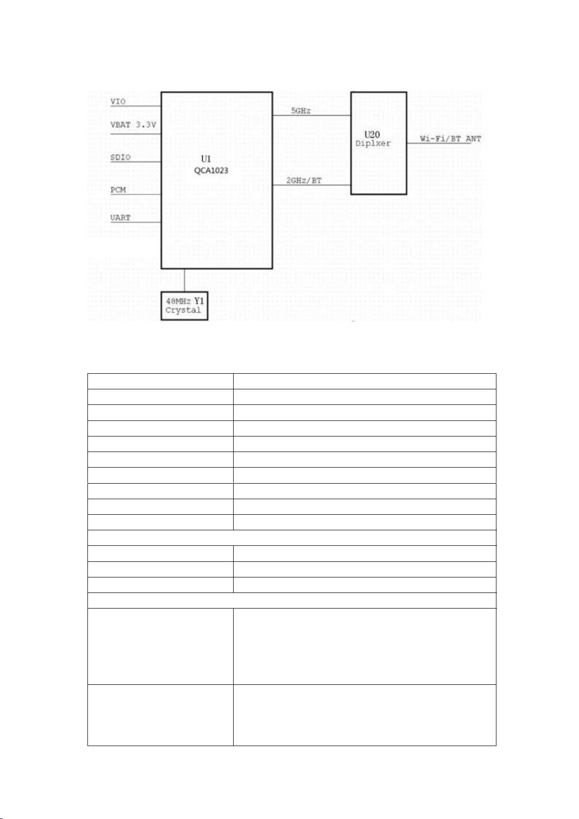
3. Block Diagram
A simplified block diagram of theYL1023 module is depicted in the figure
below。
Page 2
Model Name
YL1023
Description
Wireless LAN &Bluetooth Stamp Module
WLAN Standard
IEEE 802.11 a/b/g/n/ac
Bluetooth Standard
Bluetooth 2.1+Enhanced Data Rate (EDR)+ BT4.2
Major Chipset
QCA1023
Host Interface
Wi-Fi : SDIO, BT :UART
Dimensions
12mm * 12mm * 2.0mm
Wi-Fi VID/PID
TBD
BT VID/PID
TBD
Weight
TBD
Operating Conditions
Voltage
power supply for host:3.3V
Temperature
-40℃~85℃
Storage temperature
-45℃~135℃
Electrical Specifications
Frequency Range
WLAN:
2.4 GHz ISM Bands 2.412-2.484 GHz
5G:5.150~5.240GHz, 5.745~5.825GHz
Bluetooth:
2402~2480MHz
Modulation
DSSS, OFDM, DBPSK, DQPSK, CCK, 16-QAM, 64QAM,256-QAM for WLAN
GFSK (1Mbps), Π/4 DQPSK (2Mbps) and 8DPSK
(3Mbps) for Bluetooth
4. Specifications Table
Page 3
Output Power
WLAN:
802.11b: 19dBm (11Mbps)
802.11g: 20dBm (54Mbps)
802.11n @2.4GHz: 19dBm (HT20 MCS7)
802.11n @2.4GHz: 19dBm (HT40 MCS7)
802.11a @5GHz: 13dBm (54Mbps)
802.11a @5GHz: 13dBm (VHT20 MCS7)
802.11ac @5GHz: 13dBm (VHT20 MCS7)
802.11ac @5GHz: 13dBm (VHT40 MCS8)
802.11ac @5GHz: 13dBm (VHT80 MCS9)
Receive Sensitivity
BT: BER < 0.1% (IQXEL80 Tx -70 Bm)
Data Rates
WLAN
802.11b: 1, 2, 5.5, 11Mbps
802.11a/g: 6, 9, 12, 18, 24, 36, 48, 54Mbps
802.11n: up to 75Mbps-single
802.11n: up to 150Mbps
802.11ac:up to 96Mbps (20MHz channel)
802.11ac:up to 200Mbps (40MHz channel)
802.11ac:up to 433Mbps (80MHz channel)
Bluetooth
Bluetooth 2.1+EDR data rates of 1,2, and 3Mbps
Security
WAPI
WEP 64-bit and 128-bit encryption with H/W
TKIP processing
WPA/WPA2(Wi-Fi Protected Access)
AES-CCMP hardware implementation as part of
802.11i security
standard
Operating System
Compatibility
TBD
Symbol
Parameter
Maximum
Unit
VDD
3.3V power supply voltage
3.65
V
VDDIO
Voltage supply for GPIO
4.0
V
Symbol
Parameter
Rating
Unit
VDD
3.3V power supply voltage
3.135~3.465
V
5. Electrical Characteristics
5.1 Absolute Maximum Ratings
5.2 Recommended Operating Conditions
Page 4

VDDIO
Voltage supply for GPIO
1.71~3.46
V
Symbol
Parameter
Minimum
Typical
Maximum
Unit
VIH
Input high voltage
0.7-VIO
--
VIO+0.3
V
VIL
Input low voltage
-0.3
--
0.3-VIO
V
VOH
Output high voltage
VIO-0.4
--
VIO
V
VOL
Output low voltage
0
--
0.4
V
Pin
No.
Definition
Basic Description Type
Type
5.4 GPIO DC Characteristics
6. Pin Definition
Pin Description
Page 5

1
GND
GROUND
GND
2
WL_BT_ANT
Wi-Fi/BT RF signal
I/O
3
GND
GROUND
GND
4
NC
Floating Pin, No connect to
anything.
Floating
5
NC
Floating Pin, No connect to
anything.
Floating
6
Host_Wakeup_BT/GPIO34
Host wakeup BT device
IN 7 BT_wakeup_Host
BT Device wakeup Host
I/O
8
TMS
Reserve for EJTAG
I/O
9
VDD
DC power supply +3.3V input
VCC
10
NC
Floating Pin, No connect to
anything.
Floating
11
NC
Floating Pin, No connect to
anything.
Floating
12
WL_EN
GPIO pin to on/off the Wi-Fi
function by software. Active high.
Reserve pull high 100K resistor
and shunt 100pF
capacitor to GND on platform.
IN
13
WL_wakeup_Host/GPIO35
WLAN device wakeup host
OUT
14
SDIO_DATA2
SDIO Data Line 2
I/O
15
SDIO_DATA3
SDIO Data Line 3
I/O
16
SDIO_CMD
SDIO Command Input
I/O
17
SDIO_CLK
SDIO Clock Input
IN
18
SDIO_DATA0
SDIO Data Line 0
I/O
19
SDIO_DATA1
SDIO Data Line 1
I/O
20
GND
GROUND
GND
21
CLK_REQ/GPIO11
Clock request output
DO
22
VDDIO
1.8V-3.3V VDDIO supply for WLAN
and BT
VCC
23
NC
Floating Pin, No connect to
anything.
Floating
24
LPO
External low-power 32.768KHz clock
input.
IN
25
PCM_OUT
PCM synchronous data output,
connected to PCM_IN on the
host.
OUT
26
PCM_CLK
PCM Clock
I/O
27
PCM_IN
PCM synchronous data input,
connected to PCM_OUT on the
host.
IN
28
PCM_SYNC
PCM synchronous data SYNC
I/O
Page 6

29
TDI
Reserve for EJTAG
IN
30
TDO
Reserve for EJTAG
OUT
31
GND
GROUND
GND
32
TCK
Reserve for EJTAG
GND
33
GND
GROUND
GND
34
BT_EN
GPIO pin to on/off the BT function
by software. Active high. Reserve
pull high 100K resistor and shunt
100pF capacitor to GND on host.
IN
35
NC
Floating Pin, No connect to
anything.
Floating
36
GND
GROUND
GND
37
NC
Floating Pin, No connect to
anything.
Floating
38
NC
Floating Pin, No connect to
anything.
Floating
39
Debug_UART_TXD
TXD for Wi-Fi Uart_debug only,
connected to RXD of the host.
OUT
40
Debug_UART_RXD
RXD for Wi-Fi Uart_debug only,
connected to TXD of the host.
IN
41
UART_RTS
UART Ready To Send, connected to
CTS on the host.
OUT
42
UART_TXD
UART Transmit Data, connected to
RXD on the host.
OUT
43
UART_RXD
UART Receive Data, connected to
TXD on the host.
IN
44
UART_CTS
UART Clear To Send, connected to
RTS on the host.
IN
7 Schematics
Page 7

8 Mechanical Information
Page 8

Page 9

Declaration of Compliance
This device complies with Part 15 of the FCC Rules. Operation is subject to the
following two conditions:
(1) this device may not cause harmful interference, and
(2) this device must accept any interference received, including interference that may
cause undesired operation.
FCC RF Radiation Exposure Statement Caution: To maintain compliance with the FCC’s RF
exposure guidelines, place the product at least 20cm from nearby persons.
Warning: Changes or modifications to this unit not expressly approved by the party
responsible for compliance could void the user’s authority to operate the equipment.
This device complies with Industry Canada licence-exempt RSS standard(s).
Operation is subject to the following two conditions:
(1) this device may not cause interference, and
(2) this device must accept any interference, including interference that may cause
undesired operation of the device.
If this module absence of information to transmit or operational failure then it will
automatically discontinue transmission by software.
Le présent appareil est conforme aux CNR d'Industrie Canada applicables aux
appareils radio exempts de licence. L'exploitation est autorisée aux deux conditions
suivantes :
(1) l'appareil nedoit pas produire de brouillage, et
(2) l'utilisateur de l'appareil doit accepter tout brouillage radioélectrique subi, même si
le brouillage est susceptible d'en compromettre lefonctionnement.
This equipment complies with IC radiation exposure limits set forth for an
uncontrolled environment. This equipment should be installed and operated with
minimum distance 20cm between the radiator and your body.
Cet équipement est conforme aux limites d'exposition au rayonnement du CI établies
pour unenvironnement non contrôlé. Cet équipement doit être installé et utilisé à une
distance minimalede 20 cm entre le radiateur et votre corps.
Host labeling requirement:”Contains transmitter module FCC ID:T2C-YL1023
Host labeling requirement:”Contains transmitter module IC:10741A-YL1023
Antenna information used during testing:
Manufacturer:
Antenna type: PCB Layout antenna
Antenna gain: 3.31dBi@2400~2500MHz, 3.42dBi @5150~5850MHz
Refer to antenna specification for details.
Note: If difference antenna types are used, C2PC should be applied.
 Loading...