YAMAHA YTD436 Datasheet

YTD436
ISTC
ISDN BRI controller with S/T ref. pt. analog D/R
YTD436 is a high-performance communication LSI for the ISDN BRI user-network
interface function (digital four-wire time-division full-duplex operation), supporting D
channel layer 1 and layer 2 functions in one 100-pin SQFP chip.
YTD436 supports layer 1 (physical layer) control function conforming to ITU-T
Recommendation I.430 and fully supports layer 2 (LAPD protocol) function conforming to
ITU-T Recommendations Q.920 and Q.921. ETSI (European Telecommunication Standards
Institute) and North American standard operating modes are also supported.
In addition, YTD436 includes layer 3 processor interface function which operate in DMA
transfer mode or I/O transfer mode. This gives a great advantage for mounting and
functional designing of both “active” (CPU on board) terminal equipment and “passive” (no
CPU on board) PC cards.
The layer 1 function has a built-in S/T reference point analog driver/receiver to support the
S/T reference point interface. In order to support the U interface, YTD436 also has a I.430
TTL interface (no built-in analog driver/receiver) suitable for connecting to an NT1 chip or
a DSU module.
YTD436 CATALOG
CATALOG No.:4TD436A4
2001.1

Features
1. Layer 1 function
• Conforms to ITU-T Recommendation I.430 (1992 edition) and
• Supports ETSI ETS 300 012 (April 1992) and ANSI T1.605 operating modes
• Leased line capability (JT-I430-a)
• Built-in driver and receiver
• Abundant Test functions (for testing and maintenance)
• Multiframing capability
• INFO1 transmission and INFO4 reception monitor pins
• Power down monitor pin
• I.430 transmission frame phase adjustment function
TTC Standard JT-I430 (1997 edition) (default)
- 192 kbps transmission rate
- Interface structure : 2B + D (B = 64 kbps, D = 16 kbps)
- Frame assembling and disassembling function
- Collision control (built-in random number (Ri) reset),
priority control (built-in retransmission control), and state transition control
- Programmable T3 and T4 timers
- I.430 TTL interface (when the driver / receiver is disconnected)
- No external relay or common-mode choke needed
- Supports 1-to-2 pulse transformer
- Demo mode in which no switch simulator is needed.
- Three kinds of loop-back modes (Loop-back 1 to 3)
- INFO signals output for testing
- Test pulse output for pulse shape check
2. Layer 2 function
• Conforms to ITU-T Recommendation Q.920 (1992 edition) and Q.921 (1997 edition)
and TTC Standard JT-Q920 (1993 edition) and JT-Q921 (1998 edition)
- HDLC frame control (Flag control, FCS generation/checking,
Automatic zero insertion/deletion, Abort pattern transmission/detection, etc.)
- LAPD status control (Sequence control, Flow control, SAPI control)
- Built-in timer for time-out check
• Supports ETSI ETS 300 125 (September 1991), National ISDN-1/2,
AT&T 5ESS 5E9 and Nortel DMS-100 S208-6 operating modes
• Multilink capability
(circuit switching × 2 links, packet switching/teleaction communications × 2 links)
• Automatic assigned TEI/non-automatic assigned TEI (VC/PVC)
• Leased line mode (disable layer 2 function)
- 2 -

3. Layer 3 interface function
• Connects to 8-bit or 16-bit microprocessor
(8086 family, 80186 family, 6800 family, 68000 family)
• Operates in one of two data transfer modes :
- DMA transfer mode (with the built-in 16-bit address DMA controller)
- I/O transfer mode (with the built-in FIFO)
• Primitive logical interface
4. B channel interface
• Data rate setting : 64 k, 56 k and 32 kbps
• Serial mode
- B channel I/O clock selection function
• Internal clock mode
Inputs/outputs the B channel data with 64 k, 56 k or 32 kHz internal clock
• External clock mode (PCM Highway mode)
Inputs/outputs the B channel data with a 128 k to 2048 kHz external clock
- B channel selection function
• Internal clock mode
Selects/switches B channel I/O pins
• External clock mode (PCM Highway mode)
Selects/switches B channel time slots
• Parallel mode
- LSB/MSB switching function
- Bit shift function
- Data transfer mode
• DMA transfer mode with the DMA request function
• I/O transfer mode with the built-in FIFO
5. Low-power operation
(Host processor clock control function, Powerdown mode)
6. High-performance CMOS technology
7. 100-pin SQFP
8. DigitalSupply Voltage (+5V or +3.3V ), Analog +5V supply
- 3 -

Applications
• ISDN telephone
• Video telephone
• Telemeter
• PBX
• Terminal adapter (TA)
• Other ISDN terminals
- 4 -

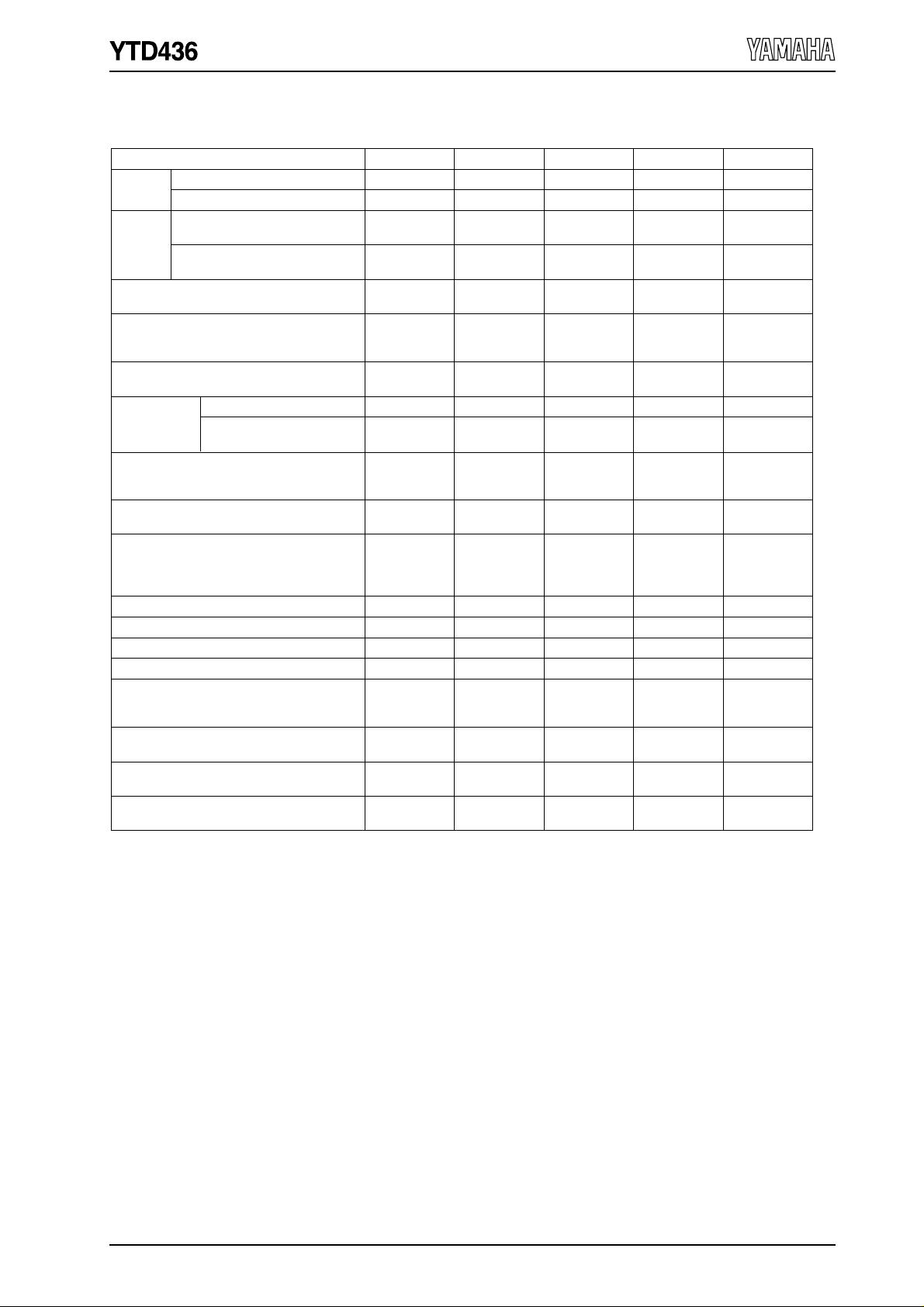
Functional Comparison of YAMAHA ISDN S/T Interface LSIs
YM7405B YTD418 YTD423 YTD436YTD410FUNCTION
Layer 1
Layer 2
(LAPD)
ETSI
ETS 300 012, ETS 300 125
North American Switches
National ISDN-1/2, AT&T 5ESS,
Nortel DMS-100
S/T Reference Point Analog Driver/Receiver
Maximum D
Channel Links
D Channel Layer 3 Data Transfer Method
HDLC Controller and
DMA Controller for B Channel Data
B Channel Data Transfer Method
B Channel Internal Clock Mode (kHz)
B Channel External Clock Mode
Clock Output Function for MPU
Signal Output Function for Testing
Supply Voltage (V)
Power Consumption
during Operation [typ.] (mW)
Power Consumption
during Sleep [typ.] (mW)
Package
ITU-T Recommendation
TTC Standard
ITU-T Recommendation
TTC Standard
Circuit Switching
Dch Packet Switching
(Teleaction Communication)
I.430
JT-I430
Q.920
Q.921
JT-Q920
JT-Q921
1992 edition
1993 edition 1993 edition 1993 edition 1993 edition
1992 edition
1993 edition 1993 edition
Internal Internal
1222
1
DMA Transfer DMA Transfer DMA Transfer
External
–––
56, 64 32, 56, 64 32, 56, 6464 64
√
√
+5
65
23021
80 pin QFP
100 pin TQFP
1992 edition 1992 edition 1992 edition 1992 edition
1992 edition 1992 edition 1992 edition
1993 edition 1993 edition
√
222
External External
√
+5 +5 +5
125 75 85
80 pin QFP
100 pin TQFP
√√√
√√
External
[YTD421B]
√√√
80 Pin QFP 100 pin SQFP100 pin SQFP
External
[YTD421B]
DMA Transfer
or
I/O Transfer
Internal Internal
DMA Transfer
or
I/O Transfer
√√
√√
1
1997 edition
1992 edition
1997 edition
1993 edition
1998 edition
Internal
2
2
(2)
DMA Transfer
or
I/O Transfer
DMA Transfer
or
I/O Transfer
(Note 1)
+5 or
+3.3
(Note 2)
75 (@+5V)
40 (@+3.3V)
less than 0.5
(Note 3)
Note 1:
Note 2:
Note 3:
DMA Transfer: Request function only
I/O transfer: 4 byte FIFO
With respect to Digital Supply Voltage
State at Line interface disconnection + Power down (SLEEP state)
- 5 -
 Loading...