YAMAHA YTD423 Datasheet

YTD423
IHDLC2
ISDN BRI controller with B-ch HDLC controllers
1 INTRODUCTION
YTD423 is a high-p erformance communication LSI for the ISDN BRI user-network interface function (digital
four-wire time-division full-duplex op eration), supporting D-channel layer 1, layer 2 and HDLC controller for B-
channels, all in one 100-pin SQFP chip. YTD423 supp orts layer 1 (physical layer) control function conforming
to ITU-T Recommendation I.430 and fully supports layer 2 (LAP-D proto col) function conforming to ITU-T
Recommendations Q.920 and Q.921. ETSI (European Telecommunications Standards Institute) and several North
American standard operating modes are also supp orted. In addition, YTD423 includes layer 3 processor interface
function and 2-channel HDLC controller for B-channels, which operate in DMA transfer mo de or I/O transfer
mode. This gives a great advantage to mounting and functional designing of both \active" (with CPU on board)
terminal equipment and \passive" (no CPU on board) PC cards. In order to supp ort the U interface, YTD423 has
aTTLinterface (no built-in analog driver/receiver) suitable for connecting to an NT1 chip or a DSU mo dule. S/T
reference p oint can also b e supp orted by connecting it to YTD421 (analog driver/receiver LSI).
1.1 Features
1. Layer 1 function
Supports layer 1 control function conforming to ITU-T Recommendation I.430 [1992 edition] and TTC
Standard JT-I430 [1993 edition] (default)
{
TTL interface
{
192 kbps transmission rate
{
Interface structure : 2B + D (B = 64 kbps, D = 16 kbps)
{
Frame assembling and disassembling function
{
Collision control (built-in random number (Ri) reset), prioritycontrol (built-in retransmission con-
trol), and state transition control
{
Programmable T3 and T4 timers
YTD423D CATALOG
CATALOG No.:4TD423D2
1999.2

Supports ETSI ETS 300 012 [April 1992] and ANSI T1.605 operating modes
Leased line capability (JT-I430-a)
Bchannel I/O clock selection function
{
Internal clockmode: Inputs/outputs the B-channel data with 64 k, 56 k or 32 kHz internal clo ck
{
External clo ck mode (PCM Highway mode): Inputs/outputs the B channel data with a 128 kHz to
2048 kHz external clock
Bchannel selection function
{
Internal clockmode: Selects/switches B channel I/O pins
{
External clo ck mo de (PCM Highway mode): Selects/switches B channel time slots
Multiframing capability
AbundantTest functions (for testing and maintenance)
{
Three kinds of loop-back mo des (Loop-back1to3)
{
INFO signals output for testing
{
Test pulse output for pulse shape evaluation
INFO1 transmission and INFO4 reception monitor pins
SLEEP monitor pin
I.430 transmission frame phase adjustment function
2. Layer 2 function
Conforms to ITU-T Recommendation Q.920 and Q.921 [1992 edition] and TTC Standard JT-Q920 and
JT-Q921 [1993 edition] (default)
{
HDLC frame control (Flag control, FCS generation/checking, automatic zero insertion/deletion,
abort pattern transmission/detection, etc.)
{
LAP-D status control (sequence control, ow control, SAPI control)
{
Built-in timer for time-out check
Supports ETSI ETS 300 125 [September 1991], National ISDN-1/2, AT&T 5ESS 5E9 and Nortel DMS-
100 S208-6 operating modes
Multi-link capability (circuit switching, packet switching)
Automatic assigned TEI/non-automatic assigned TEI (VC/PVC)
Leased line mode (disable layer 2 function)
3. Layer3interface function
Connects to 8-bit or 16-bit microprocessor (8086 family, Z80 family, 6800 family and 68000 family)
Operates in one of two data transfer modes
{
DMA transfer mode (with the built-in 24-bit address DMA controller)
{
I/O transfer mode (with the built-in FIFO)
Primitive logical interface
2

4. HDLC controller for B-channels
HDLC frame control (Flag control, optional marks or ags in idle state, optional FCS generation/checking,
automatic zero insertion/deletion, abort pattern transmission/detection, optional address eld genera-
tion/checking etc.)
Full-duplex communication22channels
Data rates Network synchronization clockmode: 56 k or 64 kbps
Network independent clo ckmode: Up to 128 kbps
Optional 16-bit/32-bit CRC
Programmable data transfer modes
{
DMA transfer mode (with the built-in DMA controller)
3
optional 8-bit/16-bit access
3
24-bit address
3
4channels
{
I/O transfer mode (with the built-in FIFO)
3
Tx FIFO : 32 bytes22
3
Rx FIFO : 64 bytes22
3
Variable interrupt levels
3
Byte/Word access selection
Optional transparent mode (disable HDLC controller function)
5. Low-power op eration (the host processor clock control function, LSI internal clo ck freezing function)
6. CMOS technology
7. 100-pin SQFP
8. Single +5V volt supply
1.2 Applications
Terminal Adapter (TA)
Router
ISDN PC Card
PBX
ISDN Telephone
3

2 BLOCK DIAGRAM
2.1 User Network Interface Blo ck Diagram
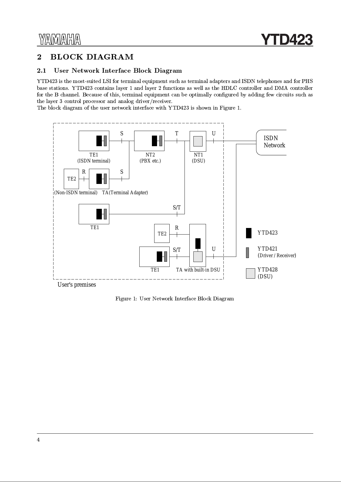
YTD423 is the most-suited LSI for terminal equipmentsuch as terminal adapters and ISDN telephones and for PHS
base stations. YTD423 contains layer 1 and layer 2 functions as well as the HDLC controller and DMA controller
for the B channel. Because of this, terminal equipment can be optimally congured by adding few circuits suchas
the layer 3 control pro cessor and analog driver/receiver.
The blo ck diagram of the user network interface with YTD423 is shown in Figure 1.
ISDN
Network
YTD423
User's premises
TE1
(ISDN terminal)
NT2
(PBX etc.)
NT1
(DSU)
TE2
(Non-ISDN terminal) TA(Terminal Adapter)
TE1
TA with built-in DSUTE1
TE2
T
S/T
R
U
RS
SU
S/T
YTD421
(Driver / Receiver)
YTD428
(DSU)
Figure 1: User Network Interface Blo ck Diagram
4
 Loading...