

YAMAHA YSS912C-F Datasheet
YSS912C
AC3D2
Dolby Digital (AC-3) / Pro Logic / DTS decoder + Sub DSP
YSS912C CATALOG
CATALOG No.:LSI-4SS912C2
1999. 3
INTRODUCTION
The YSS912C is one chip LSI consisting two built-in DSP’s ; Dolby Digital (AC-3) / Pro Logic / DTS decoder
(Main DSP) and a sound processing DSP (Sub DSP). Sub DSP is capable of realizing various sound fields, such as
virtual surround, by down-loading the program and coefficient. Sub DSP is compatible with YSS902, the Sub DSP
programs developed for YSS902 are also applicable to YSS912C.
FEATURERS
Pin compatible with YSS902 (AC3D).
Dolby Digital (AC-3) / Pro Logic and DTS decode.
24 bit DSP. (Group-A Dolby Digital decoder)
No external memory is required (Memory for center and surround channel delay is included) when DTS
decoding as well as AC-3 / Pro Logic.
Possible to decode multi-language encoded data. (possible to decode based on data-stream-number)
AC-3 karaoke mode.
Original compression mode as well as four compression modes recommended by Dolby. (when AC-3 decoding)
Included de-emphasis filter.
Pro Logic decoding for Dolby digital 2 channels decoded signal as well as ordinary PCM.
High performance 25 MIPS programmable DSP suitable for a variety of sound field processing such as original
surround , filtering, virtual surround etc.
Up to 1.36 second delay time is capable when used with an external 1Mbit SRAM. (at fs= 48 kHz)
Reads Dolby Digital (AC-3)/DTS decode information through the microprocessor interface.
Provide total sixteen I/O ports.
Possible to connect most of SPDIF receivers, A/D and D/A converters, by setting I/O data interface format.
Has a built-in PLL oscillation circuit to generates its own operating clock.
Internal operating clock is 30 MHz.
Supply Voltage: 3.3v for core logic. 5v for I/Os.
Power saving mode.
Si-gate CMOS process.
100 QFP.(YSS912C-F)
Note: "AC-3" and "Pro Logic" are registered trademarks of Dolby Laboratories Licensing Corporation.
"DTS" is a registered trademark of DTS, Inc.
Use of this LSI must be licensed by both Dolby Laboratories Licensing Corporation and DTS, Inc.
YSS912C
2
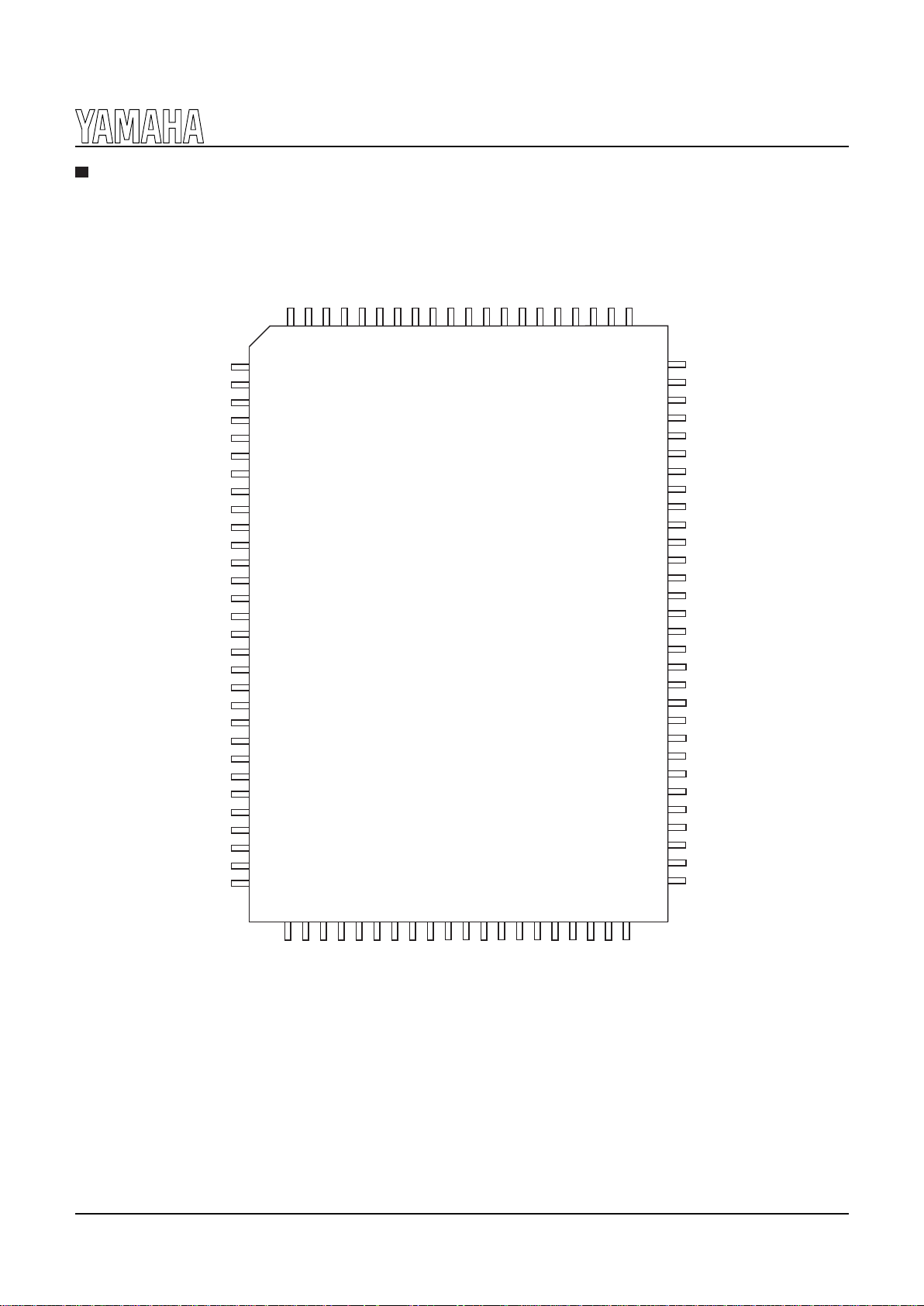
PIN CONFIGURATION
VDD1
RAMCEN
RAMA16
RAMA15
SDIB0
SDIB1
SDIB2
XI
XO
VSS
AVDD
SDIB3
TEST
TEST
AVSS
VDD2
SDOA2
SDOA1
SDOA0
RAMA14
RAMA13
RAMA12
RAMA11
RAMA10
VSS
VDD1
OPORT0
OPORT1
OPORT2
OPORT3
OPORT4
OPORT5
OPORT6
OPORT7
VSS
VDD2
RAMA9
RAMA8
RAMA7
SDOB2
SDOB1
SDOB0
SDBCK1
SDWCK1
VSS
SI
SO
VSS
RAMD7
RAMD6
RAMD5
RAMD4
RAMD3
RAMD2
RAMD1
RAMD0
VDD1
RAMA2
SCK
/CS
/CSB
RAMA3
TEST
/IC
RAMA4
VSS
RAMA5
RAMA6
/SDBCK0
SURENC
KARAOKE
MUTE
CRC
NONPCM
VDD2
VSS
IPORT0
IPORT1
IPORT2
IPORT3
IPORT4
IPORT5
IPORT6
IPORT7
VDD2
VSS
RAMOEN
RAMWEN
RAMA1
RAMA0
SDIA1
SDIA0
SDBCK0
SDWCK0
VDD2
1
2
3
4
5
6
7
8
9
10
11
12
13
14
15
16
17
18
19
20
21
22
23
24
25
26
27
28
29
30
31
323334
35
363738
39
40
41
42
43
44
454647
484950
51
52
53
54
55
56
57
58
59
60
61
62
63
64
65
66
67
68
69
70
71
72
73
74
75
76
77
78
79
80
82
83
84
85
86
87
88
89
90
91
92
93
94
95
96
97
98
99
100
81
CPO
DTSDATA
AC3DATA
SDOB3
OVFB
< 100QFP TOP VIEW >
YSS912C
3
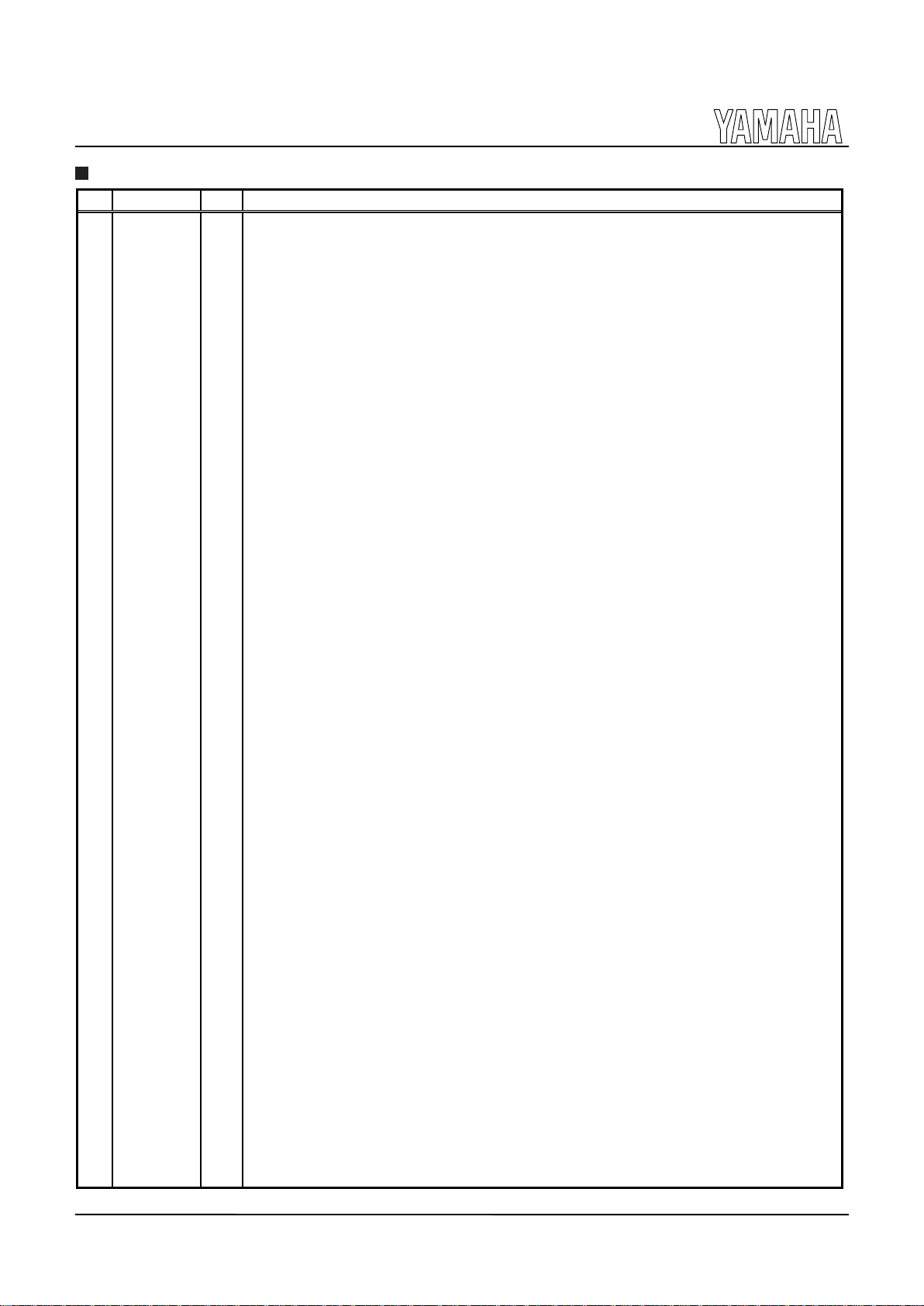
PIN FUNCTION
No. Name I/O FUNCTION
1 VDD1 -
+5V power supply (for I/Os)
2 RAMCEN O
External SRAM interface /CE
3 RAMA16 O
External SRAM interface address 16
4 RAMA15 O
External SRAM interface address 15
5SDIB0I+
PCM in
p
ut 0 to Sub DSP
6SDIB1I+
PCM in
p
ut 1 to Sub DSP
7SDIB2I+
PCM in
p
ut 2 to Sub DSP
8XI I
Cr
y
stal oscillator connection (12.288 MHz
)
9XOO
Cr
y
stal oscillator connection
10 VSS -
Ground
11 AVDD -
+3.3 V
p
ower supply (for PLL circuit
)
12 SDIB3 I+
PCM in
p
ut 3 to Sub DSP
13 TEST
Test terminal
(
to be open in normal use
)
14 TEST
Test terminal
(
to be open in normal use
)
15 OVFB O
Detection of overflow at Sub DSP
16 DTSDATA O
Detection of DTS data
17 AC3DATA O
Detection of AC-3 data
18 SDOB3 O
PCM out
p
ut from Sub DSP
19 CPO A
Out
p
ut terminal for PLL, to be connected to ground through the external analog filter circuit
20 AVSS -
Ground
(
for PLL circuit
)
21 VDD2 -
+3.3 V
p
ower supply (for core logic
)
22 SDOA2 O
PCM out
p
ut from Main DSP (C, LFE
)
23 SDOA1 O
PCM out
p
ut from Main DSP (LS, RS
)
24 SDOA0 O
PCM out
p
ut from Main DSP (L, R
)
25 RAMA14 O
External SRAM interface address 14
26 RAMA13 O
External SRAM interface address 13
27 RAMA12 O
External SRAM interface address 12
28 RAMA11 O
External SRAM interface address 11
29 RAMA10 O
External SRAM interface address 10
30 VSS -
Ground
31 VDD1 -
+5V
p
ower supply (for I/Os
)
32 OPORT0 O
Out
p
ut port for general purpose
33 OPORT1 O
Out
p
ut port for general purpose
34 OPORT2 O
Out
p
ut port for general purpose
35 OPORT3 O
Out
p
ut port for general purpose
36 OPORT4 O
Out
p
ut port for general purpose
37 OPORT5 O
Out
p
ut port for general purpose
38 OPORT6 O
Out
p
ut port for general purpose
39 OPORT7 O
Out
p
ut port for general purpose
40 VSS -
Ground
41 VDD2 -
+3.3 V
p
ower supply (for core logic
)
42 RAMA9 O
External SRAM interface address 9
43 RAMA8 O
External SRAM interface address 8
44 RAMA7 O
External SRAM interface address 7
45 SDOB2 O
PCM out
p
ut from Sub DSP
46 SDOB1 O
PCM out
p
ut from Sub DSP
47 SDOB0 O
PCM out
p
ut from Sub DSP
48 SDBCK1 I+
Bit clock in
p
ut for SDOA, SDIB, SDOB
49 SDWCK1 I+
Word clock in
p
ut for SDOA, SDIB, SDOB
50 VSS -
Ground
51 VDD2 -
+3.3 V
p
ower supply (for core logic
)
52 NONPCM O
Detection of non-PCM data
53 CRC O
Detection of AC-3 CRC error
54 MUTE O
Detection of auto mute
55 KARAOKE O
Detection of AC-3 karaoke data
YSS912C
4
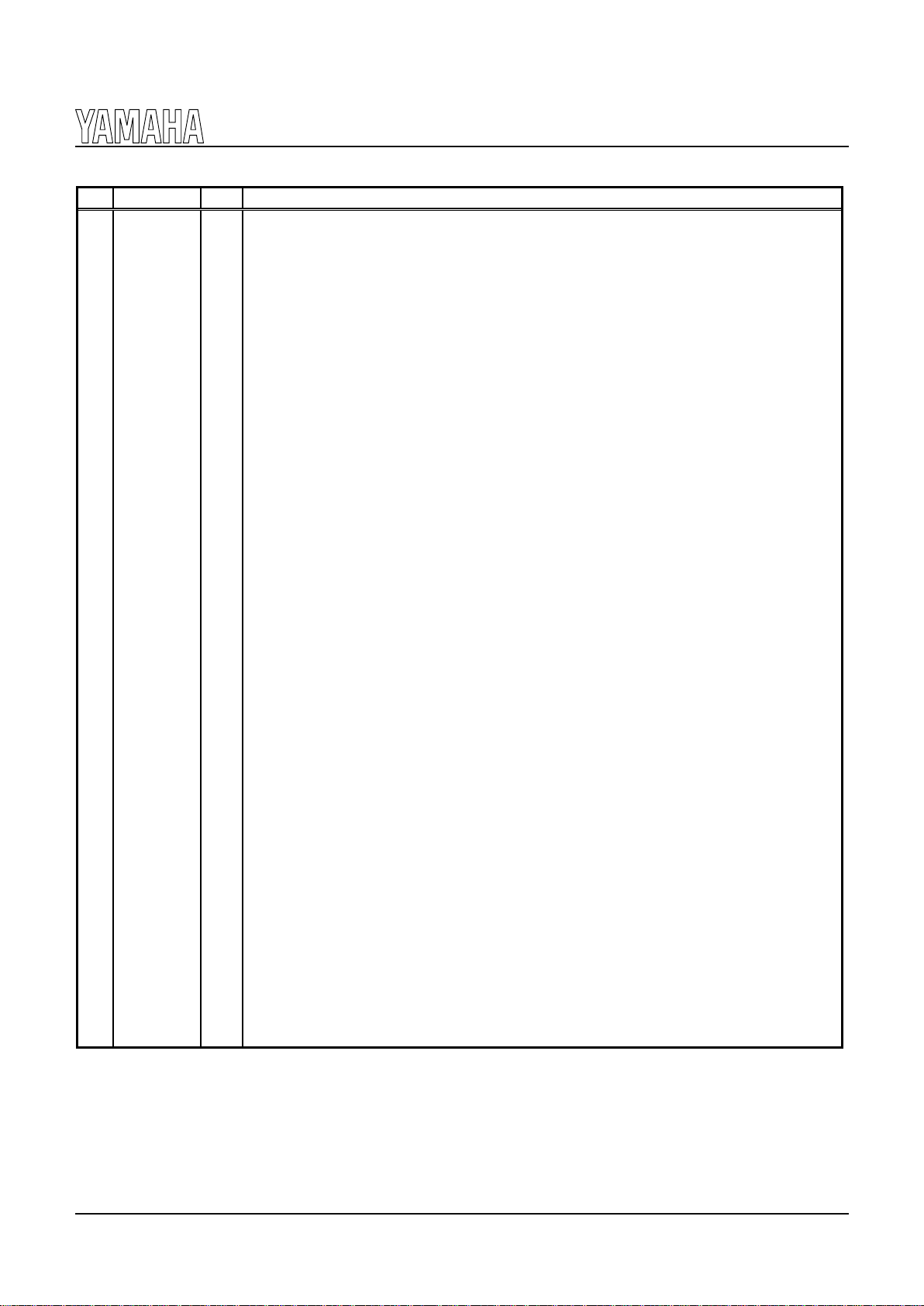
No. Name I/O FUNCTION
56 SURENC O
Detection of AC-3 2/0 mode Dolb
y
surround encoded input
57 /SDBCK0 O
Inverted SDBCK0 clock output (refer to Block diagram)
58 RAMA6 O
External SRAM interface address 6
59 RAMA5 O
External SRAM interface address 5
60 VSS -
Ground
61 RAMA4 O
External SRAM interface address 4
62 /IC Is
Initial clear
63 TEST
Test terminal (to be open in normal use)
64 RAMA3 O
External SRAM interface address 3
65 /CSB Is+
Sub DSP Chip select
66 /CS Is
Microprocessor interface Chip select input
67 SO Ot
Microprocessor interface Serial data output
68 SI Is
Microprocessor interface / Sub DSP Serial data input
69 SCK Is
Microprocessor interface / Sub DSP clock input
70 RAMA2 O
External SRAM interface address 2
71 VDD1 -
+5V power supply (for I/Os)
72 RAMD0 I+/ O
External SRAM interface data (STREAM0 output when External SRAM is not in use)
73 RAMD1 I+/ O
External SRAM interface data (STREAM1 output when External SRAM is not in use)
74 RAMD2 I+/ O
External SRAM interface data (STREAM2 output when External SRAM is not in use)
75 RAMD3 I+/ O
External SRAM interface data (STREAM3 output when External SRAM is not in use)
76 RAMD4 I+/ O
External SRAM interface data (STREAM4 output when External SRAM is not in use)
77 RAMD5 I+/ O
External SRAM interface data (STREAM5 output when External SRAM is not in use)
78 RAMD6 I+/ O
External SRAM interface data (STREAM6 output when External SRAM is not in use)
79 RAMD7 I+/ O
External SRAM interface data (STREAM7 output when External SRAM is not in use)
80 VSS -
Ground
81 VDD2 -
+3.3 V power supply (for core logic)
82 SDWCK0 I
Word clock input for SDIA, SDOA, SDIB, SDOB
83 SDBCK0 I
Bit clock input for SDIA, SDOA, SDIB, SDOB
84 SDIA0 I
AC-3 bitstream (or PCM) data input for Main DSP
85 SDIA1 I
AC-3 bitstream (or PCM) data input for Main DSP
86 RAMA1 O
External SRAM interface address 1
87 RAMA0 O
External SRAM interface address 0
88 RAMWEN O
External SRAM interface /WE
89 RAMOEN O
External SRAM interface /OE
90 VSS -
Ground
91 VDD2 -
+3.3 V power supply (for core logic)
92 IPORT7 I+
Input port for general purpose
93 IPORT6 I+
Input port for general purpose
94 IPORT5 I+
Input port for general purpose
95 IPORT4 I+
Input port for general purpose
96 IPORT3 I+
Input port for general purpose
97 IPORT2 I+
Input port for general purpose
98 IPORT1 I+
Input port for general purpose
99 IPORT0 I+
Input port for general purpose
100 VSS -
Ground
NOTE)Is: Schmidt trigger input terminal
I+
: Input terminal with a pull-up resistor
O
: Digital output terminal
Ot
: Tri-state digital output terminal
A
: Analog terminal

YSS912C
5
BLOCK DIAGRAM
CPO
XO
XI
SDOB0
SDOB1
SDOB2
SDWCK1
SDBCK1
OPORT0-7
IPORT0-7
SO
SI
SCK
/CS
OVFB
RAMA0-16
RAMOEN
RAMWEN
RAMCEN
RAMD0-7
SDIB2
SDIB1
SDIB0
SDOA2
SDOA1
SDOA0
Delay RAM
SDIASEL
SDIA1
SDIA0
SDWCK0
SDBCK0
/SDBCK0
/CSB
SCK
SI
SDOACKSEL SDIBCKSEL
SDOBCKSEL
Operating clock
(30MHz)
CRC
ERAMUSE
External RAM
SDOB Interface
24 * 16
Sub DSP
SDIB Interface
SDOA Interface
SDIBSEL
SDIA Interface
Input Buffer
decoder
24 * 24
Main DSP
AC-3/Pro Logic/DTS
Data RAM
Microprocessor
Control Registers
Control signals
Coefficient /
Program RAM
STREAM0-7
PLL
L, R
LS, RS
C, LFE
SDOB3
SDIB3
SURENC
KARAOKE
MUTE
CRC
AC3DATA
DTSDATA
NONPCM
Interface
Control signals
interface
 Loading...