

Page 1
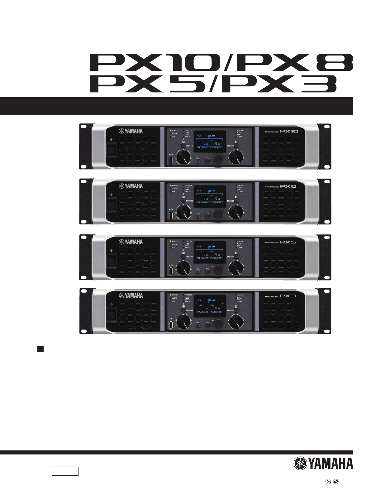
POWER AMPLIFIER
SERVICE MANUAL
SERVICE MANUAL
PX10
PX8
CONTENTS(目次)
SPECIFICATIONS(総合仕様) ....................................3
PANEL LAYOUT(パネルレイアウト) ..............................6
DIMENSIONS(寸法図) ............................................... 7
JACK AND PLUG LIST(端子とプラグ一覧) .................. 8
CIRCUIT BOARD LAYOUT(ユニットレイアウト) ..............9
DISASSEMBLY PROCEDURE(分解手順) ............... 10
LSI PIN DESCRIPTION(LSI端子機能表) ................. 18
CIRCUIT BOARDS(シート基板図) .............................21
INSPECTION(検査) ............................................ 32/61
MEASUREMENT(測定) ...................................... 53/82
UPDATING FIRMWARE(ファームウェアのアップデート)
DEVICE BACKUP(デバイスバックアップ) .................. 90
... 60/89
PX5
PX3
INITIALIZING THE PX AMPLIFIER
(PXアンプの初期化) .................................................. 92
FUNCTION LIST(機能一覧).......................................94
MESSAGE LIST(メッセ ージリスト)............................96/97
START-UP SEQUENCE(起動シーケンス) ........... 99/100
ENDING SEQUENCE(終了シーケンス) .............101/102
PARTS LIST
BLOCK DIAGRAM(ブロックダイアグラム )
LEVEL DIAGRAM(レベルダイアグラム)
WIRING(結線図)
CIRCUIT DIAGRAM(回路図)
PA
012180
HAMAMATSU, JAPAN
Copyright (c) Yamaha Corporation. All rights reserved. PDF ’16.10
Page 2
PX10/PX8/PX5/PX3
IMPORTANT NOTICE
This manual has been provided for the use of authorized Yamaha Retailers and their service personnel. It has been assumed that basic service procedures inherent to the industry, and more specifically Yamaha Products, are already known and understood by the users, and have
therefore not been restated.
WARNING : Failure to follow appropriate service and safety procedures when servicing this product may result in personal injury, de-
IMPORTANT : This presentation or sale of this manual to any individual or firm does not constitute authorization certification, recog-
The data provided is believed to be accurate and applicable to the unit(s) indicated on the cover. The research engineering, and service
departments of Yamaha are continually striving to improve Yamaha products. Modifications are, therefore, inevitable and changes in
specification are subject to change without notice or obligation to retrofit. Should any discrepancy appear to exist, please contact the
distributor’s Service Division.
WARNING : Static discharges can destroy expensive components. Discharge any static electricity your body may have accumulated by
struction of expensive components and failure of the product to perform as specified. For these reasons, we advise all
Yamaha product owners that all service required should be performed by an authorized Yamaha Retailer or the appointed
service representative.
nition of any applicable technical capabilities, or establish a principal-agent relationship of any form.
grounding yourself to the ground bus in the unit (heavy gauge black wires connect to this bus.)
IMPORTANT : Turn the unit OFF during disassembly and parts replacement. Recheck all work before you apply power to the unit.
WARNING: This product contains chemicals known to the State of California to cause cancer, or birth defects or other reproductive harm.
DO NOT PLACE SOLDER, ELECTRICAL/ELECTRONIC OR PLASTIC COMPONENTS IN YOUR MOUTH FOR ANY REASON WHAT SO EVER!
Avoid prolonged, unprotected contact between solder and your skin! When soldering, do not inhale solder fumes or expose eyes to solder/ flux
vapor!
If you come in contact with solder or components located inside the enclosure of this product, wash your hands before handling food.
IMPORTANT NOTICE FOR THE UNITED KINGDOM
Connecting the Plug and Cord
WARNING: THIS APPARATUS MUST BE EARTHED IMPORTANT. The wires in this mains lead are coloured in accordance with
the following code:
GREEN-AND-YELLOW : EARTH
BLUE : NEUTRAL
BROWN : LIVE
As the colours of the wires in the mains lead of this apparatus may not correspond with the coloured markings identifying the
terminals in your plug proceed as follows:
The wire which is coloured GREEN-and-YELLOW must be connected to the terminal in the plug which is marked by the letter E
or by the safety earth symbol
The wire which is coloured BLUE must be connected to the terminal which is marked with the letter N or coloured BLACK.
The wire which is coloured BROWN must be connected to the terminal which is marked with the letter L or coloured RED.
or colored GREEN or GREEN-and-YELLOW.
(3 wires)
WARNING
Components having special characteristics are marked and must be replaced with parts having specification equal to those
originally installed.
印の部品は、安全を維持するために重要な部品です。交換する場合は、安全のために必ず指定の部品をご使用ください。
WARNING
Please keep the USB cap out of reach of children, to keep them from accidentally swallowing it.
USBキャップは、子供が誤って飲み込まないように、子供の手の届かないところに保管してください。
mark indicates a dangerous electrically live terminal. When connecting an external wire to
This
this terminal, it is necessary either to have “a person who have received appropriate guidance on
handling” make the connection or to use leads or a cord that have been manufactured in such a
way that the connection can be made simply and without problem.
マークは、危険活電部であることを示します。この端子への外部からの配線接続は、適正な取扱指導を
受けた者が行なうか、問題なく容易に接続できるように製作されたリ−ド線、またはコードを使用する
必要があります。
2
Page 3
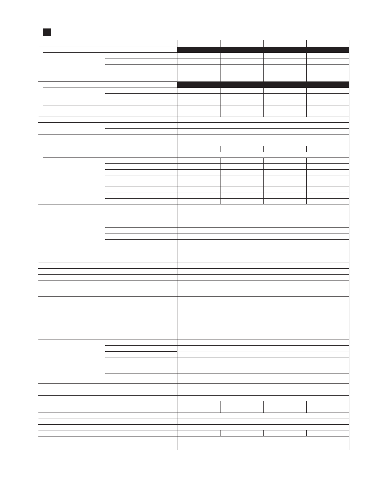
SPECIFICATIONS(総合仕様)
Output Power
1 kHz, non-clip, 20 msec burst,
both channels driven
1 kHz, non-clip, 20 msec burst
Output Power
1 kHz, non-clip, 20 msec burst,
both channels driven
1 kHz, non-clip, 20 msec burst
Amplifier Type (Output Circuitry)
THD+N
Frequency Response
Crosstalk
S/N Ratio
Voltage Gain/Sensitivity
8Ω, volume max.
8Ω, volume max.,
Power Boost mode
Load Protection
Amplifier Protection
Power Supply Protection
Cooling
Maximum Input Voltage
Input Impedance
Sampling Frequency
A/D, D/A Converters
Signal Processing
Latency
User Amplifier Preset
Factory Speaker Preset
Connectors
Controls
Indicators
AC Power Requirement
Power Consumption
Operating Temperature
Storage Temperature
Dimensions (W × H × D)
Net Weight
Included accessories
*1 Device operation has been confirmed within ±10% of the rated power supply voltage.
(出力)
(出力)
(全高調波歪率)
(周波数特性)
(クロストーク)
(S/N 比)
(負荷保護)
(アンプ保護)
(冷却)
(入力インピーダンス)
(サンプリング周波数)
(AD、DA コンバーター)
(信号処理)
(遅延)
(端子)
(操作子)
(インジケーター)
(消費電力)
(保存温度)
(質量)
8Ω 1000 W × 2 800 W × 2 500 W × 2 300 W × 2
4Ω 1200 W × 2 1050 W × 2 800 W × 2 500 W × 2
2Ω 700 W × 2 600 W × 2 500 W × 2 300 W × 2
8Ω/Power Boost Mode — — 800 W × 1 600 W × 1
4Ω/Power Boost Mode — — 1400 W × 1 1000 W × 1
8Ω 1000 W × 2 800 W × 2 500 W × 2 300 W × 2
4Ω 1200 W × 2 1050 W × 2 800 W × 2 500 W × 2
2Ω 700 W × 2 600 W × 2 500 W × 2 300 W × 2
8Ω/Power Boost Mode — — 800 W × 1 600 W × 1
4Ω/Power Boost Mode — — 1200 W × 1 1000 W × 1
(増幅方式(出力回路))
1 kHz, 10 W 0.1%
1 kHz, half power 0.3%
1 W, 8Ω, 20 Hz to 20 kHz ±1.0 dB
Half power, 8Ω, 1 kHz, vol. max., input 150Ω shunt
A-weighted, 8Ω, gain setting = +14 dBu
(電圧利得 / 感度)
(電源保護)
(最大入力電圧)
(ユーザーアンププリセット)
(出荷時スピーカープリセット)
(電源条件)
(使用温度)
(外形寸法)
(付属品)
Gain setting: 32 dB 32.0 dB/+9.3 dBu 32.0 dB/+8.3 dBu 32.0 dB/+6.3 dBu 32.0 dB/+4.1 dBu
Gain setting: 26 dB 26.0 dB/+15.3 dBu 26.0 dB/+14.3 dBu 26.0 dB/+12.3 dBu 26.0 dB/+10.1 dBu
Gain setting: +4 dBu 37.3 dB/+4 dBu 36.3 dB/+4 dBu 34.3 dB/+4 dBu 32.1 dB/+4 dBu
Gain setting: +14 dBu 27.3 dB/+14 dBu 26.3 dB/+14 dBu 24.3 dB/+14 dBu 22.1 dB/+14 dBu
Gain setting: 32 dB — — 34.0 dB/+6.3 dBu 35.0 dB/+4.1 dBu
Gain setting: 26 dB — — 28.0 dB/+12.3 dBu 29.0 dB/+10.1 dBu
Gain setting: +4 dBu — — 36.3 dB/+4 dBu 35.1 dB/+4 dBu
Gain setting: +14 dBu — — 26.3 dB/+14 dBu 25.1 dB/+14 dBu
POWER switch on/off Output mute
Output voltage protection Over voltage limiter, user configurable by wattage and speaker preset
DC-fault Power supply shutdown (NOT restored automatically)
Thermal Output limiter (Restored automatically) → Output mute (Restored automatically)
Over current Output mute (Restored automatically)
Over voltage Output limiter (Restored automatically)
Integrated Power Limit Output limiter (Restored automatically)
Thermal Output limiter (Restored automatically) → Power supply shutdown
Over voltage Power supply shutdown
Over current Power supply shutdown
Analog input to speakers 1.5 msec
Analog input XLR-3-31 × 2, 1/4" PHONE(TRS) × 2
Speakers Neutrik speakON NL4 × 2, binding post × 2 pairs, 1/4" PHONE(TS) × 2
AC IN AC inlet × 1 with AC cord clamp
USB
Front Panel
Display
1/8 MAX power, 4Ω, Pink noise at all channels
Idle, 4Ω 60 W 60 W 55 W 55 W
(定格電源電圧の± 10% の電圧で動作することを確認しています。)
PX10/PX8/PX5/PX3
PX10 PX8 PX5 PX3
Class D, balanced output circuit (BTL)
101 dB
HPF/LPF: cutoff frequency 20 Hz–20 kHz with polarity control
USB 2.0 Standard-A connector (female) for save/load, speaker preset update, firmware update with USB flash drive
POWER switch, 31 step volume knob × 2, rotary encoder and switches for GUI control
Operation lock feature (Full lock or Lock except volume and mute)
POWER × 1 (green), ALERT × 1 (red), USB × 1 (green), PROTECT × 2 (red), CLIP/LIMIT × 2 (red),
Depending on area of purchase; 100 V 50 Hz/60 Hz, 120 V 60 Hz, 220 V-240 V 50 Hz/60 Hz
310 W 280 W 230 W 160 W
7.4 kg (16.31 lbs) 7.2 kg (15.87 lbs) 6.9 kg (15.21 lbs) 6.9 kg (15.21 lbs)
• AC power cord • Owner’s Manual • Technical Specifications (English) • AC plug clamp • USB cap
(•電源コード•3芯−2芯変換プラグ•取扱説明書•TechnicalSpecifications(スペックシート、英文)
120 V 60 Hz, 220 V-240 V 50 Hz/60 Hz
100 V 50 Hz/60 Hz
(ClassD、バランス出力回路(BTL))
-60 dB
101 dB 100 dB 100 dB
16 step variable speed fan × 2, front to rear airflow
20 kΩ (Balance), 10 kΩ (Unbalance)
AD: 24-bit linear, 128 times over sampling
DA: 24-bit linear, 128 times over sampling
D-CONTOUR: FOH/MAIN, MONITOR, OFF
Speaker processor: 6 band PEQ + Limiter + Delay
Speaker presets for Yamaha passive speakers
128 × 64 pixel, mono color with brightness adjustment
SIGNAL × 2 (green),Auto LED off feature
480 × 88 × 388 mm (18.90 × 3.46 × 15.28 inch)
•電源コード誤脱防止クランプ•USBキャップ)
≦
+24 dBu
48 kHz
Input summing
Delay: 0–74msec
8 user amplifier presets
Auto display off feature
0°C to +40°C
-20°C to +60°C
*1
3
Page 4
PX10/PX8/PX5/PX3
Current draw and thermal dissipation
•
(消費電流と熱放散)
Testsignal:Pinknoise(bandwidthlimitedfrom22Hzto22kHz),1Btu=1,055.06J=0.252kcal,(W)×0.86=kcal
(テスト信号:ピンクノイズ(22Hz から 22kHz に帯域制限 )、1BTU=1,055.06J=0.252kcal、1W=0.86kcal)
●
PX10
Idle
(アイドル)
1/8 out
1/3 out
Idle
(アイドル)
1/8 out
1/3 out
Idle
(アイドル)
1/8 out
1/3 out
Line current (A)
100 V/50 Hz
8Ω/ch 2.6 213 125 88 300 76
4Ω/ch 3.1 261 150 111 379 95
8Ω/ch 5.6 472 333 139 474 120
4Ω/ch 7.2 608 400 208 710 179
110 V-120 V/60 Hz
8Ω/ch 2.2 213 125 88 300 76
4Ω/ch 2.7 263 150 113 386 97
8Ω/ch 4.6 466 333 133 454 114
4Ω/ch 5.9 597 400 197 672 169
220 V-240 V/50 Hz
8Ω/ch 1.4 219 125 94 321 81
4Ω/ch 1.6 271 150 121 413 104
8Ω/ch 2.7 471 333 138 471 119
4Ω/ch 3.3 602 400 202 689 174
(線電流)
100 V
0.8 57 0 57 195 49
Line current (A)
(線電流)
120 V
0.7 60 0 60 205 52
Line current (A)
(線電流)
230 V
0.5 62 0 62 212 53
Power consumption (In)
(消費電力)
Power consumption (In)
(消費電力)
Power consumption (In)
(消費電力)
Watt (W)
(電力)
Power consumption (Out)
(消費電力)
Watt (W)
(電力)
Power consumption (Out)
(消費電力)
Watt (W)
(電力)
Power consumption (Out)
(消費電力)
Watts dissipated
(放散電力)
Watts dissipated
(放散電力)
Watts dissipated
(放散電力)
Thermal dissipation
(熱放散)
Btu/h kcal/h
Thermal dissipation
(熱放散)
Btu/h kcal/h
Thermal dissipation
(熱放散)
Btu/h kcal/h
●
PX8
Idle
1/8 out
1/3 out
Idle
1/8 out
1/3 out
Idle
1/8 out
1/3 out
(アイドル)
110 V-120 V/60 Hz
(アイドル)
220 V-240 V/50 Hz
(アイドル)
Line current (A)
100 V/50 Hz
8Ω/ch 2.2 178 100 78 266 67
4Ω/ch 2.9 237 131 106 362 91
8Ω/ch 4.6 386 267 119 406 102
4Ω/ch 6.4 543 350 193 659 166
8Ω/ch 1.9 182 100 82 280 71
4Ω/ch 2.5 237 131 106 362 91
8Ω/ch 3.8 385 267 118 403 101
4Ω/ch 5.4 542 350 192 655 165
8Ω/ch 1.2 184 100 84 287 72
4Ω/ch 1.5 242 131 111 379 95
8Ω/ch 2.2 385 267 118 403 101
4Ω/ch 3.0 544 350 194 662 167
(線電流)
100 V
0.8 57 0 57 195 49
Line current (A)
(線電流)
120 V
0.7 60 0 60 205 52
Line current (A)
(線電流)
230 V
0.5 62 0 62 212 53
Power consumption (In)
(消費電力)
Power consumption (In)
(消費電力)
Power consumption (In)
(消費電力)
Watt (W)
(電力)
Power consumption (Out)
(消費電力)
Watt (W)
(電力)
Power consumption (Out)
(消費電力)
Watt (W)
(電力)
Power consumption (Out)
(消費電力)
Watts dissipated
(放散電力)
Watts dissipated
(放散電力)
Watts dissipated
(放散電力)
Thermal dissipation
Btu/h kcal/h
Thermal dissipation
Btu/h kcal/h
Thermal dissipation
Btu/h kcal/h
(熱放散)
(熱放散)
(熱放散)
4
Page 5
●
PX5
Idle
1/8 out
1/3 out
(アイドル)
PX10/PX8/PX5/PX3
Line current (A)
100 V/50 Hz
8Ω/ch 1.9 122 63 59 201 51
4Ω/ch 2.7 189 100 89 304 77
8Ω/ch 3.6 253 167 86 293 74
4Ω/ch 5.6 424 267 157 536 135
(線電流)
100 V
0.8 46 0 46 157 40
Power consumption (In)
(消費電力)
Watt (W)
(電力)
Power consumption (Out)
(消費電力)
Watts dissipated
(放散電力)
Thermal dissipation
Btu/h kcal/h
(熱放散)
●
Idle
1/8 out
1/3 out
Idle
1/8 out
1/3 out
PX3
Idle
1/8 out
1/3 out
110 V-120 V/60 Hz
(アイドル)
220 V-240 V/50 Hz
(アイドル)
(アイドル)
Line current (A)
(線電流)
120 V
8Ω/ch 1.7 130 63 67 229 58
4Ω/ch 2.4 196 100 96 328 83
8Ω/ch 3.1 259 167 92 314 79
4Ω/ch 4.8 428 267 161 549 138
8Ω/ch 1.0 130 63 67 229 58
4Ω/ch 1.4 197 100 97 331 83
8Ω/ch 1.9 259 167 92 341 79
4Ω/ch 2.9 434 267 167 570 144
100 V/50 Hz
8Ω/ch 1.5 94 38 56 191 48
4Ω/ch 2.0 137 63 74 253 64
8Ω/ch 2.6 174 100 74 253 64
4Ω/ch 3.9 285 167 118 403 101
0.8 54 0 54 184 46
Line current (A)
(線電流)
230 V
0.5 57 0 57 195 49
Line current (A)
(線電流)
100 V
0.8 46 0 46 157 40
Power consumption (In)
(消費電力)
Power consumption (In)
(消費電力)
Power consumption (In)
(消費電力)
Watt (W)
(電力)
Power consumption (Out)
(消費電力)
Watt (W)
(電力)
Power consumption (Out)
(消費電力)
Watt (W)
(電力)
Power consumption (Out)
(消費電力)
Watts dissipated
(放散電力)
Watts dissipated
(放散電力)
Watts dissipated
(放散電力)
Thermal dissipation
Btu/h kcal/h
Thermal dissipation
Btu/h kcal/h
Thermal dissipation
Btu/h kcal/h
(熱放散)
(熱放散)
(熱放散)
Idle
(アイドル)
1/8 out
1/3 out
Idle
(アイドル)
1/8 out
1/3 out
Line current (A)
110 V-120 V/60 Hz
8Ω/ch 1.3 100 38 62 212 53
4Ω/ch 1.8 140 63 77 263 66
8Ω/ch 2.3 183 100 83 283 71
4Ω/ch 3.4 291 167 124 423 107
220 V-240 V/50 Hz
8Ω/ch 0.8 101 38 63 215 54
4Ω/ch 1.1 142 63 79 270 68
8Ω/ch 1.4 181 100 81 276 70
4Ω/ch 2.1 293 167 126 430 108
(線電流)
120 V
0.8 54 0 54 184 46
Line current (A)
(線電流)
230 V
0.5 57 0 57 195 49
Power consumption (In)
(消費電力)
Power consumption (In)
(消費電力)
Watt (W)
(電力)
Power consumption (Out)
(消費電力)
Watt (W)
(電力)
Power consumption (Out)
(消費電力)
Watts dissipated
(放散電力)
Watts dissipated
(放散電力)
Thermal dissipation
(熱放散)
Btu/h kcal/h
Thermal dissipation
(熱放散)
Btu/h kcal/h
5
Page 6
PX10/PX8/PX5/PX3
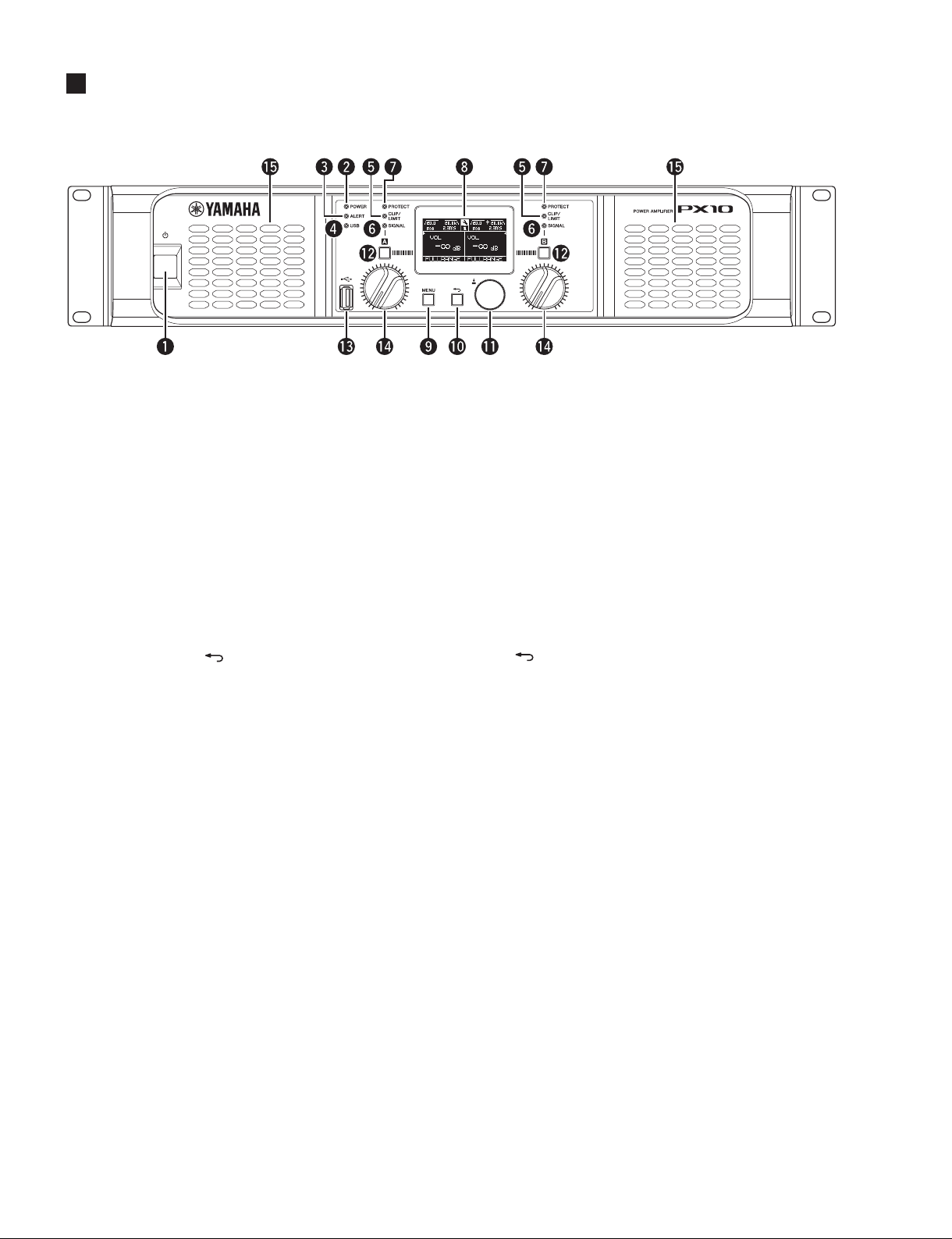
PANEL LAYOUT(パネルレイアウト)
• Front Panel
(フロントパネル)
q Power button
w [POWER] indicator
e [ALERT] indicator
r [USB] indicator
t [CLIP/LIMIT] indicators
y [SIGNAL] indicators
u [PROTECT] indicators
q 電源ボタン
w [POWER]インジケーター
e [ALERT]インジケーター
r [USB]インジケーター
t [CLIP/LIMIT]インジケーター
y [SIGNAL]インジケーター
u [PROTECT]インジケーター
i Display
o [MENU] key
!0 [
!1 Main knob
!2 [A]/[B] keys
!3 [USB] terminal
!4 Volume knobs
!5 Intake ports
] (Back) key
i ディスプレイ
o [MENU]キー
!0 [
!1 メインノブ
!2 [A]/[B]キー
!3 [USB] 端子
!4 ボリュームノブ
!5 吸気口
](バック)キー
6
Page 7
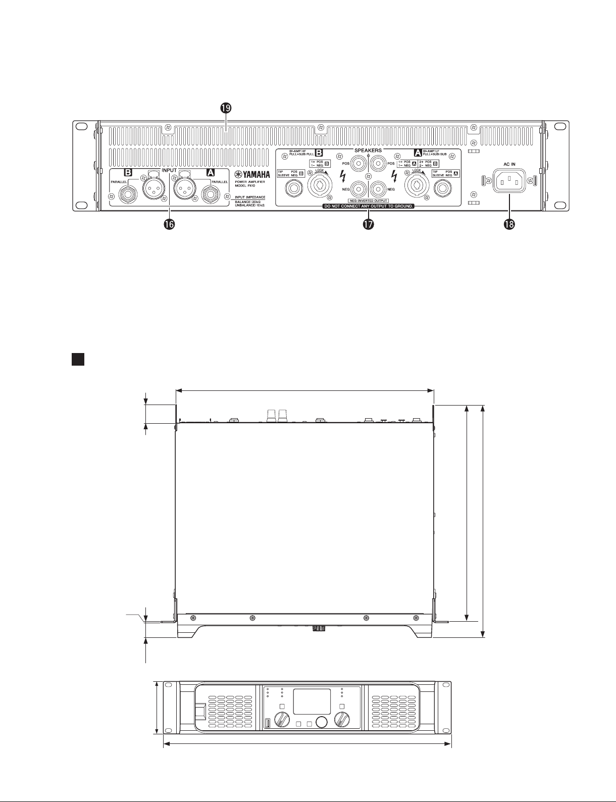
PX10/PX8/PX5/PX3
• Rear Panel
(リアパネル)
!6 [INPUT] A/B connectors
!7 [SPEAKERS] A/B terminals
!8 AC IN connector
!9 Exhaust ports
DIMENSIONS(寸法図)
!6 [INPUT]A/B端子
!7 [SPEAKERS]A/B端子
!8 ACIN端子
!9排気口
2.5
430
29
388
361 (Mounting Surface to Rear End)
24.5
88
480
unit(単位): mm
7
Page 8
PX10/PX8/PX5/PX3
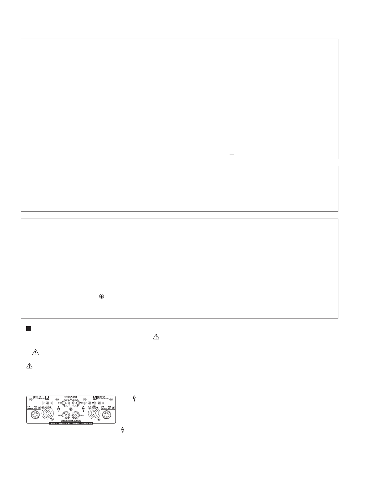
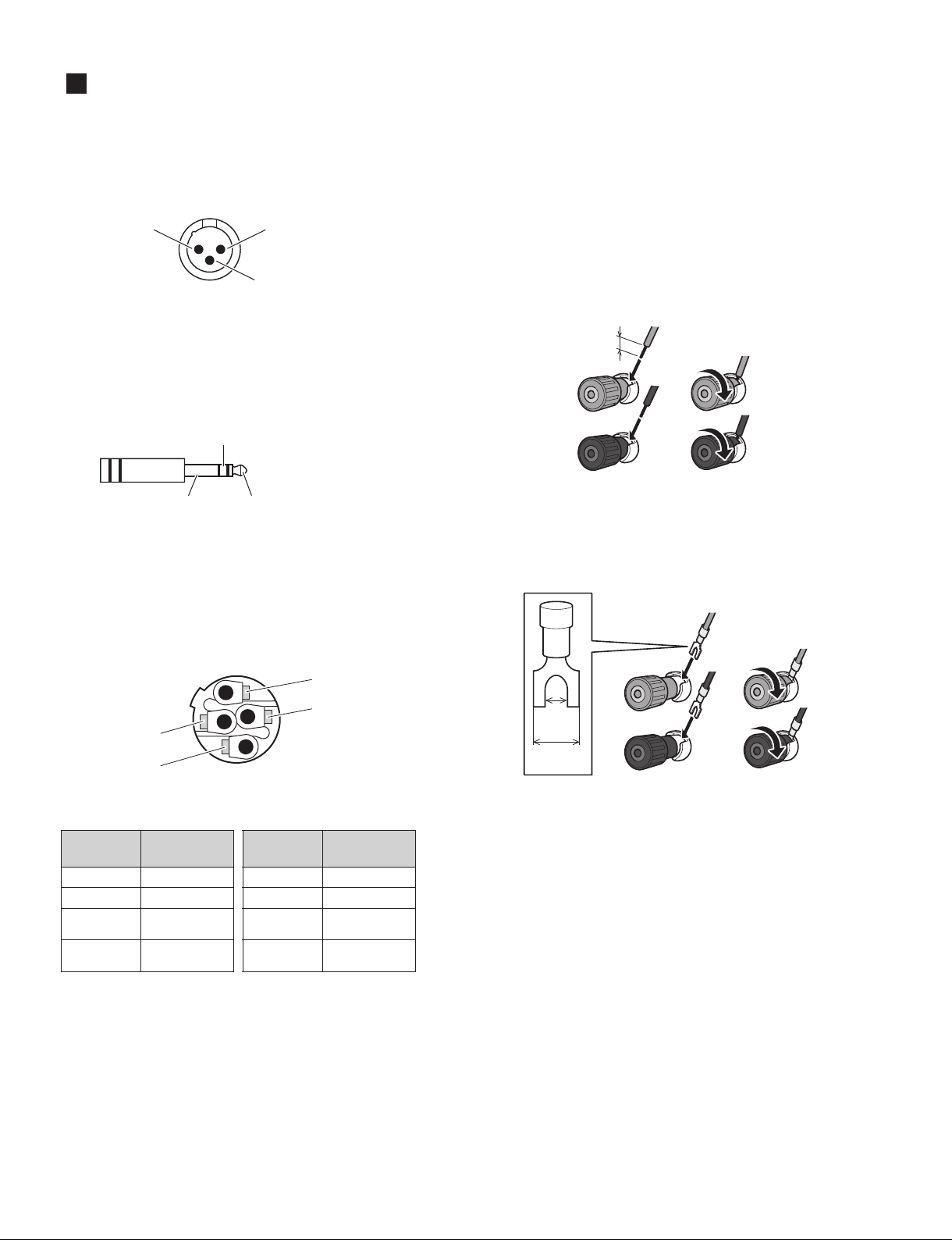
JACK AND PLUG LIST(端子とプラグ一覧)
• XLR jack
XLR type 3-31 jack.
(XLR端子)
(XLR型3-31タイプの端子です。)
The polarity is shown below (IEC60268).
(極性は次のとおりです(IEC60268)。)
Hot(ホット)
• Phone jack
21
3
(フォーン端子)
Ground(グラウンド)
Cold(コールド)
Balanced TRS phone jack.
(バランス型のTRSフォーン端子です。)
The polarity of the connections is shown below.
(接続する極性は次のとおりです。)
Ring (cold)(リング(コールド))
(スリーブ(グラウンド))
• SpeakON connector
Tip (hot)(チップ(ホット))Sleeve (ground)
(スピコン端子)
Insert the SpeakON cable plug (Neutrik NL4) into the
connector, and turn it to the right to lock it.
(スピコンケーブルプラグ(NeutrikNL4)を差し込み、
右に回してロックします。)
• Binding post connector
• Without plugs
Remove about 15 mm of insulation from the end of each
speaker cable, pass the bare wire through the holes in the
appropriate speaker terminals, and tighten the terminals to
securely clamp the wires. Make sure that the bare wire ends do
not jut out from the terminals and touch the chassis.
(スピーカーケーブルの先端の被覆を15mm外し、端子の穴に通
して締め付けます。このとき、芯線がシャーシに当たらないよう
にしてください。)
• Y-plugs
From above, insert the Y-plugs all the way into the opening, and
tighten the terminals.
(Y型プラグを上から奥まで差し込み、締め付けます。)
(プラグなしの場合)
15 mm
(Y型プラグの場合)
(バインディングポスト端子)
1+
1–
Channel A (Aチャンネル)
Neutrik NL4
1+ A+
1– A–
2+ B+
2– B–
PX amplifier
(PXアンプ)
2–
2+
Channel B (Bチャンネル)
Neutrik NL4
1+ B+
1– B–
2+
2–
PX amplifier
(PXアンプ)
not connected
(接続なし)
not connected
(接続なし)
0.25"
(6.3 mm)
≤0.51"
(12.9 mm)
8
Page 9

CIRCUIT BOARD LAYOUT(ユニットレイアウト)
PX10/PX8/PX5/PX3
• Top view
(上から見た図)
AC INLET
(ACインレット)
OUT
AUDIO
PS
ACIN
• Front view
PSW
DC FAN
(DCファン)
(前面から見た図)
PF
VOL
DC FAN
(DCファン)
FPN
USB ENC
9
Page 10
PX10/PX8/PX5/PX3
DISASSEMBLY PROCEDURE(分解手順)
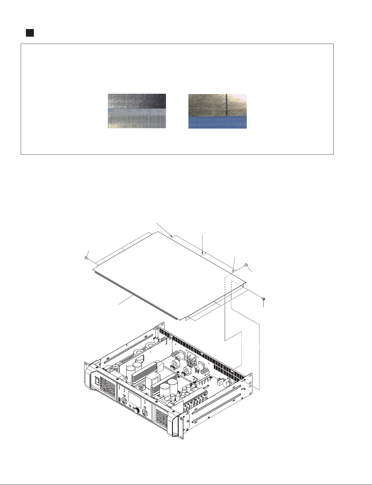
Caution:
• Install the binding tie and the cord clamp in the same way
as they were before removal.
• Pay attention not to insert and install the FFC cable to the
connector inversely. (Photo A)
Front Side
(表面)
Photo A
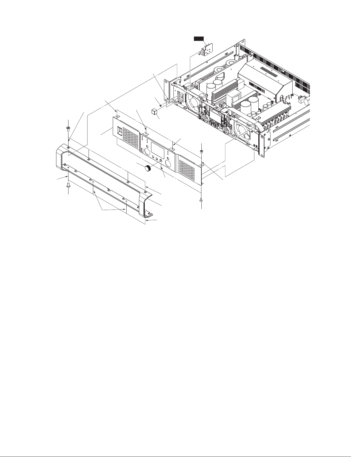
1. Top Panel (Time required: About 2 minutes)
1-1 Remove the nine (9) screws marked [1120]. The top panel
can then be removed. (Fig. 1)
* When installing the top panel, first tighten the priority
screws as shown in Fig. 1.
Priority screw (2nd)
(優先ネジ2)
注意事項
•インシュロックタイ、束線止めは、取り外す前と同じように取り
付けてください。
•FFCケーブルの表・裏を逆に差し込まないように注意して取り
付けてください。(写真A)
Back Side
(裏面)
(写真 A)
1. トップパネル
1-1 [1120]のネジ 9 本を外して、トップパネルを外します。
(図1)
※ トップパネルを取り付ける際は、優先ネジを図1に示す順
で締めてください。
Priority screw (1st)
(優先ネジ1)
(所要時間:約2 分)
[1120]
TOP PANEL
(トップパネル)
Priority screw (2nd)
(優先ネジ2)
[1120]
[1120]
10
Fig. 1
(図1)
Page 11
<Top view (上面)>
AC INLET
(ACインレット)
[860] [440] [440]
[350]
Priority screw (2nd)
(優先ネジ2)
[520]
PX10/PX8/PX5/PX3
Priority screw (1st)
(優先ネジ1)
[340]
<Rear view (背面)>
[670]
ACIN
HEXAGONAL NUT
(六角ナット)
Priority screw (3rd)
(優先ネジ3)
CB901
Priority screw (2nd)
[520]
AUDIO
[670]
OUT
CB902
PS
(優先ネジ2)
HEXAGONAL NUT
(六角ナット)
Priority screw (3rd)
(優先ネジ3)
PF
[470A]
Priority screw (1st)
(優先ネジ1)
Priority screw (2nd)
(優先ネジ2)
[430]
AUDIO
OUT
[630]
Tighten the screws marked [330] with
holding the inlet angle.
(インレット金 具を押さえながら[330]のネジを
締めてください 。)
[640]
Priority screw (2nd)
(優先ネジ2)
[620]
Priority screw (1st)
(優先ネジ1)
[420]
Priority screw (1st)
(優先ネジ1)
Fig. 2
2.
ACIN Circuit Board (Time required: About 4 minutes)
2-1 Remove the top panel. (See procedure 1.)
2-2 Remove the cable tie marked [860]. (Fig. 2)
2-3 Remove the two (2) screws marked [330], the nine (9)
screws marked [340] and the screw marked [350]. The
ACIN circuit board can then be removed.(Fig. 2)
* When installing the ACIN circuit board, first tighten the
screws marked [330] with holding the inlet angle.
(Fig. 2)
3.
PS Circuit Board (Time required: About 6 minutes)
3-1 Remove the top panel. (See procedure 1.)
3-2 Remove the ten (10) screws marked [520]. The PS circuit
board can then be removed.(Fig. 2)
* When installing the PS circuit board, first tighten the
priority screws as shown in Fig. 2.
HEXAGONAL NUT
(六角ナット)
Priority screw (3rd)
(優先ネジ3)
[330]
ACIN
(図2)
2. ACINシート
(所要時間:約4 分)
2-1 トップパネルを外します。(1項参照)
2-2 [860]のインシュロックタイを外します。(図2)
2-3 [330]のネジ2 本と[340]のネジ 9 本、[350]のネジ1本を
外して、ACINシート外します。(図2)
※ ACINシー トを取り付ける際は、先に[330]のネジをイン
レット金具を押さえながら締めてください。(図2)
3. PSシート
(所要時間:約6 分)
3-1 トップパネルを外します。(1項参照)
3-2 [520]のネジ10 本を外して、PSシート外します。
(図2)
※ PSシートを取り付ける際は、優先ネジを図2に示す順で締
めてください。
[330]
INLET ANGLE
(インレット金具)
11
Page 12
PX10/PX8/PX5/PX3
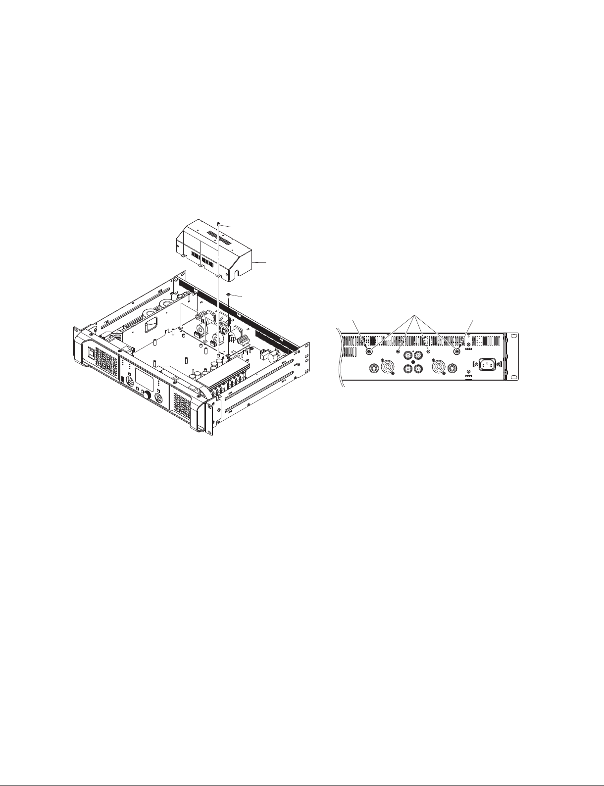
4.
OUT Circuit Board (Time required: About 8 minutes)
4-1 Remove the top panel. (See procedure 1.)
4-2 Remove the seven (7) screws marked [830]. The shield out
can then be removed. (Fig. 3)
* When installing the shield OUT, first tighten the priority
screws as shown in Fig. 3.
4-3 Remove the three (3) screws marked [440]. (Fig. 2, 3)
4-4 Remove the screw marked [420], the four (4) screws
marked [430] and the two (2) hexagonal nuts. The OUT
circuit board can then be removed. (Fig. 2)
* When installing the OUT circuit board, first tighten the
priority screws as shown in Fig. 2.
[830]
[440]
SHIELD OUT
(シールドOUT)
4. OUTシート
(所要時間:約8 分)
4-1 トップパネルを外します。(1項参照)
4-2 [830]のネジ7 本を外して、シールド OUTを外します。
(図3)
※ シールドOUTを取り付ける際は、優先ネジを図3に示す順
で締めてください。
4-3 [440]のネジ3 本を外します。(図2、3)
4-4 [420]のネジ1 本と[430]のネジ 4 本、六角ナット2 個を外
して、OUTシートを外します。(図2)
※ OUTシートを取り付ける際は、優先ネジを図2に示す順で
締めてください。
<Rear view (背面)>
Priority screw (1st)
(優先ネジ1)
[830]
Priority screw (2nd)
(優先ネジ2)
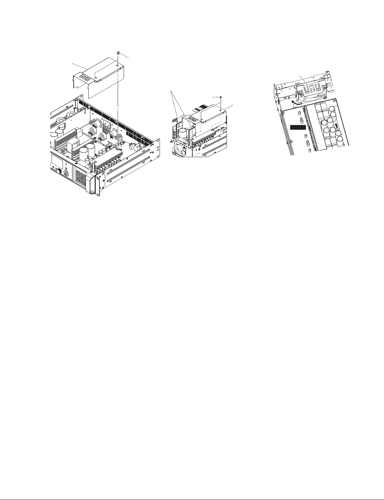
5. AUDIO
Circuit Board
(Time required: About 8 minutes)
5-1 Remove the top panel. (See procedure 1.)
5-2 Remove the shield out. (See procedure 4-2.)
5-3 Remove the connectors of the CB901 and CB902 from
OUT circuit board. (Fig. 2)
5-4 Remove the PS circuit board. (See procedure 3.)
5-5 PX10/PX8 only
Remove the two (2) plastic rivets marked [850]. The duct
amp can then be removed. (Fig. 4)
* When installing the duct amp, fit the tabs of duct amp
into the slots of sub chassis. (Fig. 4)
5-6 Remove the nine (9) screws marked [630]. (Fig. 2)
5-7 Remove the four (4) screws marked [620], the two (2)
screws marked [640], the two (2) hexagonal nuts, the two
(2) washers and the two (2) plastic washers marked [670].
The AUDIO circuit board can then be removed. (Fig. 2)
* When installing the AUDIO circuit board, first tighten
the priority screws as shown in Fig. 2.
* PX5/PX3 only : When installing the AUDIO circuit board,
AUDIO circuit board with bending FFC guard as shown
in Fig. 4.
Fig. 3
(図3)
5. AUDIOシート
(所要時間:約8 分)
5-1 トップパネルを外します。(1項参照)
5-2 シールドOUTを外します。(4-2 項参照)
5-3 OUTシートからCB901とCB902のコネクタを 外し
ます。(図2)
5-4 PSシートを外します。(3項参照)
5-5 PX10/PX8のみ
[850]のプラスチックリベット2個を外して、ダクト
AMPを外します。(図4)
※ ダクトAMPを取り付ける際は、ダクトAMPのタブをサブ
シャーシの長孔に挿し入れます。(図4)
5-6 [630]のネジ9 本を外します。(図2)
5-7 [620]のネジ 4 本と[640]のネジ 2 本、六角ナット2個と
ワッシャー 2個、[670]のプラワッシャー 2個を外して、
AUDIOシートを外します。(図2)
※ AUDIOシートを取り付ける際は、優先ネジを図2に示す順
で締めてください。
※ PX5/PX3 のみ:AUDIOシートを取り付ける際は、FFCガー
ドを曲げながらAUDIOシー トを取り付けてください。
(図4)
12
Page 13
r1919 r1919
Set AUDIO circuit board with bending FFC guard.
DUCT AMP
(ダクトAMP)
[850]
Fit the tabs of duct amp into the slots of sub chassis.
(ダクトAMPのタブをサブシャーシの長孔に挿し入れます。)
[850]
Fig. 4
(図4)
DUCT AMP
(ダクトAMP)
(FFCガードを曲げながらAUDIOシートを 取り付 け てください 。)
PX10/PX8/PX5/PX3
FFC GUARD
(FFCガード)
AUDIO
6. PF
Circuit Board
(Time required: About 3 minutes)
6-1 Remove the top panel. (See procedure 1.)
6-2 Remove the four (4) screws marked [470A]. The PF circuit
board can then be removed. (Fig. 2)
* When installing the PF circuit board, first tighten the
priority screws as shown in Fig. 2.
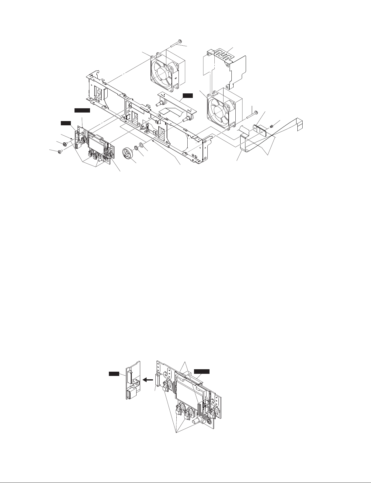
7. Front Panel Assembly
(Time required: About 4 minutes)
7-1 Remove the top panel. (See procedure 1.)
7-2 Remove the eight (8) screws marked [960]. The front
frame can then be removed. (Fig. 5)
7-3 Remove the seven (7) screws marked [940] and the knob
ENCDR. The front panel assembly can then be removed.
(Fig. 5)
* When installing the front frame and front panel
assembly, first tighten the priority screws as shown in
Fig. 5.
8. PSW
Circuit Board
(Time required: About 4 minutes)
8-1 Remove the top panel. (See procedure 1.)
8-2 Remove the front panel assembly. (See procedure 7.)
8-3 Remove the two (2) screws marked [100] and power
switch knob. The PSW circuit board can then be removed.
(Fig. 5)
* When installing the PSW circuit board, first tighten the
priority screws as shown in Fig. 5.
6. PFシート
(所要時間:約3 分)
6-1 トップパネルを外します。(1項参照)
6-2 [470A]のネジ 4本を外して、PFシートを外します。
(図2)
※ PFシートを取り付ける際は、優先ネジを図2に示す順で締
めてください。
7. Fパネル Ass'y
(所要時間:約4 分)
7-1 トップパネルを外します。(1項参照)
7-2 [960]のネジ 8 本を外して、フロントフレームを外し
ます。(図5)
7-3 [940]の ネジ7本 と ノブ ENCDRを外して、Fパネル
Ass'yを外します。(図5)
※ フロントフレームとFパネルAss'yを取り付ける際は、優先
ネジを図5に示す順で締めてください。
8. PSWシート
(所要時間:約4 分)
8-1 トップパネルを外します。(1項参照)
8-2 FパネルAss'yを外します。(7 項参照)
8-3 [100]のネジ2 本とPSWノブを外して、PSWシートを
外します。(図5)
※ PSWシートを取り付ける際は、優先ネジを図5に示す順で
締めてください。
13
Page 14
PX10/PX8/PX5/PX3
Priority screw (1st)
(優先ネジ1)
PSW
Priority screw (2nd)
(優先ネジ2)
Priority screw (4th)
(優先ネジ4)
[960]
Priority screw (3rd)
(優先ネジ3)
FRONT PANEL
ASSEMBLY
(FパネルAssy)
Priority screw (1st)
(優先ネジ1)
KNOB ENCDR
(ノブENCDR)
[100]
POWER SWITCH KNOB
Priority screw (4th)
(優先ネジ4)
[960]
Priority screw (3rd)
(優先ネジ3)
Fig. 5
9. Front Panel Section
(Time required: About 8 minutes)
9-1 Remove the top panel. (See procedure 1.)
9-2 Remove the front panel assembly. (See procedure 7.)
9-3 Remove the connector of the CB103 from ACIN circuit
board. (Fig. 6)
9-4 Remove the cable tie marked [750]. (Fig. 6)
9-5 Remove the five (5) screws marked [720]. The shield
ACIN can then be removed. (Fig. 6)
* When installing the shield ACIN, first tighten the priority
screws as shown in Fig. 6.
9-6 Remove the six (6) screws marked [1020]. The right and
left rack angles can then be removed. (Fig. 6)
* When installing the rack angles, first tighten the priority
screws as shown in Fig. 6.
9-7 Remove the screw marked [470B]. (Fig. 6)
9-8 Remove the seven (7) screws marked [270]. The front
panel section can then be removed. (Fig. 6)
* When installing the front panel section, first tighten the
priority screws as shown in Fig. 6.
* When installing the front panel section, fit the claws
of side panels (L/R) into the notches of front panel
sectoin, fit the claw of front panel section into the notch
of bottom assembly. (Fig. 7)
(PSWノブ)
Priority screw (2nd)
(優先ネジ2)
Priority screw (4th)
(優先ネジ4)
FRONT FRAME
(フロントフレーム )
Priority screw (1st)
(優先ネジ1)
(図5)
[940]
Priority screw (3rd)
(優先ネジ3)
[940]
9. フロントパネル部
(所要時間:約8 分)
9-1 トップパネルを外します。(1項参照)
9-2 FパネルAss'yを外します。(7 項参照)
9-3 ACINシートからCB103のコネクタを外します。(図6)
9-4 [750]のインシュロックタイを外します。(図6)
9-5 [720]のネジ5本を外して、シールドACINを外します。
(図6)
※ シールドACINを取り付ける際は、優先ネジを図6に示す順
で締めてください。
9-6 [1020]のネジ 6 本を外して、左右のラック金具を外し
ます。(図6)
※ ラック金具を取り付ける際は、優先ネジを図6に示す順で
締めてください。
9-7 [470B]のネジ1 本を外します。(図6)
9-8 [270]のネジ 7本を外して、フロントパネル部を外し
ます。(図6)
※ フロントパネル部を取り付ける際は、優先ネジを図6に示
す順で締めてください。
※ フロントパネル部を取り付ける際は、切り欠きをサイドパ
ネル(L/R)のツメに挿し込み、ツメをボトム Ass'yの切り欠
きに挿し込みます。(図7)
14
Page 15
Priority screw (2nd)
(優先ネジ2)
Priority screw (3rd)
(優先ネジ3)
RACK ANGLE
(ラック金具)
[720]
SHIELD ACIN
(シールドACIN)
<Rear view (背面)>
Priority screw (1st)
(優先ネジ1)
[720]
PX10/PX8/PX5/PX3
[1020]
Priority screw (3rd)
(優先ネジ3)
[270]
Priority screw (1st)
(優先ネジ1)
Priority screw (2nd)
(優先ネジ2)
Priority screw (1st)
(優先ネジ1)
FRONT PANEL SECTION
(フロントパネル 部)
CB103
• Rear view of the Front panel section
FRONT PANEL SECTION
[750]
[470B]
[270]
Priority screw (2nd)
(優先ネジ2)
Fig. 6
(図6)
(フロントパネル部を裏から見た図)
(フロントパネル 部)
Priority screw (3rd)
(優先ネジ3)
RACK ANGLE
(ラック金具)
NOTCH(切り欠き)
Be careful not to let wire bundles get pinched here.
(間に束線を挟みこまないようにしてください 。)
[270]
Priority screw (2nd)
(優先ネジ2)
Priority screw (2nd)
(優先ネジ2)
Priority screw (1st)
(優先ネジ1)
[1020]
NOTCH
(切り欠き)
NOTCH
SIDE PANEL R
(サイドパネルR )
NOTCH
(切り欠き)
CLAW
(ツメ)
(切り欠き)
Disassembly of the Front panel section.
*
Before disassembly, remove the front panel section in advance.
(See procedure 9 on page 14.)
10. VOLCircuit Board
(Time required: About 8 minutes)
10-1 Remove the two (2) knobs marked [910]. (Fig. 8)
10-2 Remove the two (2) hexagonal nuts and the two (2) flat
washers marked [140]. The VOL circuit board can then be
removed. (Fig. 8)
* When installing the VOL circuit board, first tighten the
priority nut as shown in Fig. 8.
BOTTOM ASSEMBLY
(ボトムAssy)
Fig. 7
(図7)
10. VOLシート
10-1 [910]のノブVR2 個を外します。(図8)
10-2 六角ナット2個と[140]の平座金VR2個を外して、
※ VOLシートを取り付ける際は、優先ナットを図8に示す順
CLAW
(ツメ)
SIDE PANEL L
(サイドパネルL )
フロントパネル部の分解
※ あらかじめフロントパネル部を外しておきます。
(14ページの9項参照)
(所要時間:約8 分)
VOLシートを外します。(図8)
で締めてください。
15
Page 16
PX10/PX8/PX5/PX3
(with ENC circuit board)
USB
Priority screw (2nd)
(優先ネジ2)
[80]
[90]
FPN CS
DC FAN
(DCファン)
Priority screw (1st)
(優先ネジ1)
[140]
HEXAGONAL NUT
(六角ナット)
[910]
Priority nut (1st)
(優先ナット1)
Fig. 8
(図8)
[40]
DC FAN
(DCファン)
VOL
FFC GUARD : PX5/PX3 onry
(FFCガード:PX5/PX3のみ)
[40]
Attach the holder FFC so as to match
FFC CABLE
(FFCケーブル)
the bend of FFC cable.
(ホルダーFFCをFFCケーブルの曲げに
合わせて貼り付けます。)
HOLDER FFC
(ホルダーFFC)
[880]
11. FPN CS (with ENC Circuit Board), USB
Circuit Board
11-1 Remove the four (4) screws marked [80] and the screw
marked [90]. The FPN CS circuit board and USB circuit
board can then be removed. (Fig. 8)
11-2 Remove the USB circuit board from the connector on the
CB106 of FPN CS circuit board. (Fig. 9)
11-3 Remove the four (4) button-tact switches from FPN CS
circuit board. (Fig. 9)
* When installing the FPN CS circuit board, first tighten
the priority screws as shown in Fig. 8.
* The two (2) cushions are not parts of the FPN CS circuit
board. Install the new cushions when replacing the FPN
CS circuit board. (Fig. 9)
* Attach the cushion on FPN CS circuit board in accordance
with the dashed line so as to cover the screw as shown
in Fig. 9.
(Time required: About 9 minutes)
USB
CB106
11. FPNCS(ENCシート付)、USBシート
(所要時間:約9 分)
11-1 [80]のネジ 4 本 と[90]の ネジ 1 本を外して、FPN CS
シートとUSBシートを外します。(図8)
11-2 FPNCSシートのCB106 のコネクタからUSBシート
を外します。(図9)
11-3 FPNCSシートより、ボタンタクトスイッチ4 個を外
します。(図9)
※ FPNCSシートを取り付ける際は、優先ネジを図8 に示す順
で締めてください。
※ クッション 2 個は、FPNCSシートの構成部品ではありま
せん。FPN CSシートを交換する際は、新しいクッション
を取り付けてください。(図9)
※ クッションを図9 に示すように、破線を基準にして、ネジを
覆うようにFPNCSシートへ貼り付けてください。
CUSHION
(クッション)
(with ENC circuit board)
FPN CS
16
BUTTON-TACT SWITCH
(ボタンタクトスイッチ )
Fig. 9
(図9)
Page 17
PX10/PX8/PX5/PX3
12. DC FAN (Time required: About 9 minutes)
12-1 Remove the eight (8) screws marked [40]. The DC fans
can then be removed. (Fig. 8)
* Remove the along with the FFC guard is the PX5 / PX3.
* When installing the DC fan, align the wire bundle of DC
fan in the “△” mark on sub chassis. (Fig. 10)
* When installing the DC fan, install DC fan so that label
surface can be secn. (Fig. 10)
* PX5/PX3 only : FFC in attach FFC guard to the side of
sub chassis having the “○” mark. (Fig. 10)
SUB CHASSIS
(サブシャーシ)
LABEL
(ラベル)
12. DCファン
(所要時間:約9 分)
12-1 [40]のネジ8 本を外して、左右のDCファンを外しま
す。(図8)
※ PX5/PX3 は、FFCガードと共に外します。
※ DCファンを取り付ける際は、束線をサブシャーシの「△」刻
印の方向に合わせて取り付けてください。(図10)
※ DCファンを取り付ける際は、DCファンのラベル面が見え
るように取り付けてください。(図10)
※ PX5/PX3 のみ:FFCガードは「○」刻印がある側に取り付
けてください。(図10)
DC FAN
(DCファン)
FFC GUARD
(FFCガード)
LABEL
(ラベル)
Fig. 10
13. FFC Cable (Time required: About 8 minutes)
13-1 Remove the plastic rivet [880] and press from the front.
The holder FFC can then be removed. (Fig. 8)
13-2 Remove the FFC cable from the holder FFC. (Fig. 8)
* When installing the FFC cable, after bending the FFC
cable as shown in Fig. 11, it bends to crest folding in the
position of an alternate long and short dash line, and
then insert to the connector.
* Attach the holder FFC so as to match the bend of FFC
cable. (Fig. 8)
• The bending size of a FFC cable
(FFCケーブルの折り曲げ寸法)
20 ± 2
Terminal Side
(端子面)
140 ± 2
(図10)
13. FFCケーブル
(所要時間:約8 分)
13-1 [880]のプラスチックリベットを正面側から押して、
ホルダー FFCを外します。(図8)
13-2
ホルダー FFCからFFCケーブルを取り外します。(図8)
※ FFCケーブルを取り付ける際は、図11のように折り曲げた
後、一点鎖線の位置で山折りに折り曲げ、コネクタに挿入し
ます。
※ ホルダー FFCをFFCケーブルの曲げに合わせて貼り付け
ます。(図8)
Crest folding
(山折り)
15 ± 2
90°
Crest folding
Crest folding
(山折り)
(山折り)
Protection plate side
(保護板面)
Fig. 11
(図11)
20 ± 2
As shown in a figure, after bending,
it bends to crest folding in the position
of an alternate long and short dash line.
(図の様に折り曲げた後、一点鎖線の位置
で山折りに折り曲げます。)
17
Page 18
PX10/PX8/PX5/PX3
LSI PIN DESCRIPTION(LSI 端子機能表)
AK4382AVT (X0661A00) DAC (Digital to Analog Converter) ...............................................................18
LPC1820FBD144,551 (YF570B00) MCU (Microcontroller Unit) ..........................................................19
NJW1194V(TE1) (X8355A00) 2-CHANNEL ELECTRONIC VOLUME ............................................... 18
PCM1804DBR (X6872A01) ADC (Analog to Digital Converter) ...........................................................18
YDA177-VZ (YF978A00) DIGITAL POWER AMPLIFIER ....................................................................20
YSS952-QZE2A (YE441A00) DSP(SPR-2) (Digital Signal Processor) ................................................20
AK4382AVT (X0661A00) DAC (Digital to Analog Converter)
PIN
NAME I/O FUNCTION
NO.
1
MCLK
2
BICK
3
SDTI
4
LRCK
5
PDN
6
CSN
7
CCLK
8
CDTI
I
I
I
I
I
I
I
I
Master Clock
Audio Serial Data Clock
Audio Serial Date Input
L/R Clock
Power Down mode
Chip Select
Control Data Input
Control Data Input
PIN
NAME I/O FUNCTION
NO.
9
10
11
12
13
14
15
16
AOUTRAOUTR+
AOUTL-
AOUTL+
Vss
VDD
DZFR
DZFL
O
O
O
O
-
O
O
Rch Analog out(-)
Rch Analog out(+)
Lch Analog out(-)
Lch Analog out(+)
Ground
Power Supply
Rch Data Zero Input Detect
Lch Data Zero Input Detect
NJW1194V(TE1) (X8355A00) 2-CHANNEL ELECTRONIC VOLUME
PIN
NO.
1
2
3
4
5
6
7
8
9
10
11
12
13
14
15
16
InA1
InA2
InA3
InA4
GND
DCCAP_A
GND
OutA
VDDOUT
DATA
CLOCK
LATCH
GND
Tone_Tr1a
Tone_Ba1a
Tone_Ba2a
I/O FUNCTIONNAME
I
Ach Input 1
I
Ach Input 2
I
Ach Input 3
I
Ach Input 4
-
Ground
-
Switching noise rejection capacitor (Ach)
-
Ground
O
Ach Output
O
Internal Digital Power Supply output
I
Control data signal input
I
Clock signal input
I
Latch signal input
-
Ground
-
Ach Treble Filter Terminal 1
-
Ach Bass Filter Terminal 1
-
Ach Bass Filter Terminal 2
PIN
NO.
17
18
19
20
21
22
23
24
25
26
27
28
29
30
31
32
Tone_Ba2b
Tone_Ba1b
Tone_Tr1b
GND
V -
V +
ADR0
ADR1
OutB
GND
DCCAP_B
GND
InB4
InB3
InB2
InB1
I/O FUNCTIONNAME
-
Bch Bass Filter Terminal 2
-
Bch Bass Filter Terminal 1
-
Bch Treble Filter Terminal 1
Ground
Power Supply (-)
Power Supply (+)
Chip address setting terminal 0
I
Chip address setting terminal 1
I
Bch Output
O
Ground
Switching noise rejection capacitor (Bch)
Ground
Bch Input 4
I
Bch Input 3
I
Bch Input 2
I
Bch Input 1
I
AUDIO: IC416
AUDIO: IC422
PCM1804DBR (X6872A01) ADC (Analog to Digital Converter)
18
PIN
NO.
1
2
3
4
5
6
7
8
9
10
11
12
13
14
15
V
REFL
AGNDL
V
COML
INL+
V
V
INL–
FMT0
FMT1
S/M
OSR0
OSR1
OSR2
BYPAS
DGND
DD
V
DATA/DSDR
I/O FUNCTIONNAME
-
L-channel voltage reference output,
requires capacitors for decoupling to AGND
-
Analog ground for VREFL
-
L-channel analog common-mode voltage (2.5 V)
I
L-channel analog input, positive pin
I
L-channel analog input, negative pin
I
Audio data format 0
I
Audio data format 1
I
Slave/master mode selection
I
Oversampling ratio 0
I
Oversampling ratio 1
I
Oversampling ratio 2
I
HPF bypass control
-
Digital ground
-
Digital power supply +3.3 V
O
L-channel and R-channel audio data output in PCM
mode / R-channel audio data output in DSD mode
PIN
NO.
16
BCK/DSDL
17
LRCK/DSDBCK
18
SCKI
19
RST
20
OVFR
21
OVFL
22
23
AGND
24
VINR–
25
VINR+
26
VCOMR
27
AGNDR
28
V
V
CC
REFR
I/O FUNCTIONNAME
I/O
I/O
Bit clock input/output in PCM mode /
L-channel audio data output in DSD mode
Sampling clock input/output in PCM and
DSD modes
I
System clock input
I
Reset, power-down input, active-low
O
Overflow signal of R-channel in PCM mode
O
Overflow signal of L-channel in PCM mode
-
Analog power supply +5 V
-
Analog ground
I
R-channel analog input, negative pin
I
R-channel analog input, positive pin
-
R-channel analog common-mode voltage (2.5 V)
-
Analog ground for VREFR
-
R-channel voltage reference output,
requires capacitors for decoupling to AGND
AUDIO : IC417
Page 19
PX10/PX8/PX5/PX3
LPC1820FBD144, 551 (YF570B00) MCU
PIN
NO.
1
GPIO2 [0
2
ADC0_1
3
GPIO2
4
VSSIO
5
VDDIO
6
DAC
7
GPIO2
8
GPIO2 [2
9
GPIO2 [4
10
GPIO2 [5
11
GPIO2 [6
12
XTAL1
13
XTAL2
14
I2S1_TX_SCK
15
GPIO5 [12
16
USB0_VDDA3V3_DRIVER
17
USB0_VDDA3V3
18
USB0_DP
19
USB0_VSSA_TERM
20
USB0_DM
21
USB0_VBUS
22
USB0_ID
23
USB0_VSSA_REF
24
USB0_RREF
25
VDDREG
26
TDI
27
TCK
28
DBGEN
29
TRST
30
TMS
31
TDO
32
GPIO0
33
GPIO5 [13
34
I2S1_TX_SDA
35
GPIO5 [14
36
VDDIO
37
GPIO2
38
GPIO0 [4
39
GPIO2 [10
40
VSSIO
41
VDDIO
42
BOOT
43
BOOT [1
44
SSP1_MISO
45
SSP1_SCK
46
GPIO2
47
SSP1_MOSI
48
SSP1_SSEL
49
GPIO1
50
GPIO1 [10
51
GPIO1 [1
52
GPIO1 [2
53
GPIO1 [3
54
GPIO2 [12
55
GPIO1 [4
56
GPIO1 [5
57
GPIO2 [13
58
GPIO2 [14
59
VDDREG
60
GPIO1
61
GPIO1 [7
62
GPIO0 [2
63
GPIO2 [15
64
GPIO0 [3
65
GPIO2 [7
66
GPIO0 [12
67
GPIO0 [13
68
CLKOUT
69
GPIO5
70
GPIO0 [15
71
VDDIO
72
GPIO4
[1]
[3]
[0]
[9]
[0]
[11]
[9]
[6]
[18]
[11]
I/O FUNCTIONNAME
]
I/O
General purpose digital input/output pin
I
ADC input channel 1
I/O
General purpose digital input/output pin
-
Ground
-
I/O power supply +3.3 V
I
ADC input channel 0
I/O
]
I/O
]
I/O
]
]
]
]
]
]
]
]
]
]
]
]
]
]
]
]
]
]
]
]
]
]
]
]
]
General purpose digital input/output pin
I/O
I/O
Input to the oscillator circuit and internal clock generator circuits
I
Output from the oscillator amplifier
O
Transmit Clock
I/O
General purpose digital input/output pin
I/O
Separate analog 3.3 V power supply for driver
USB 3.3 V separate power supply voltage
USB0 bidirectional D+ line
I/O
Dedicated analog ground for clean reference for termination resistors
USB0 bidirectional D- line
I/O
VBUS pin (power on USB cable)
I/O
Indicates to the transceiver whether connected as an
I
A-device (USB0_ID LOW) or B-device (USB0_ID HIGH)
Dedicated clean analog ground for generation of reference currents and voltages
-
12.0 kΩ (accuracy 1 %) on-board resistor to ground for current reference
Main regulator power supply +3.3 V
Test Data In for JTAG interface
I
Test Clock for JTAG interface
I
JTAG interface control signal
I
Test Reset for JTAG interface
I
Test Mode Select for JTAG interface
I
Test Data Out for JTAG interface
O
I/O
General purpose digital input/output pin
I/O
2
I
S1 transmit data
I/O
General purpose digital input/output pin
I/O
I/O power supply +3.3 V
-
I/O
General purpose digital input/output pin
I/O
I/O
Ground
I/O power supply +3.3 V
-
I/O
Boot pin
I/O
Master In Slave Out for SSP1
I/O
Serial clock for SSP1
I/O
General purpose digital input/output pin
I/O
Master Out Slave in for SSP1
I/O
Slave Select for SSP1
I/O
I/O
I/O
I/O
I/O
I/O
General purpose digital input/output pin
I/O
I/O
I/O
I/O
I/O
Main regulator power supply +3.3 V
-
I/O
I/O
I/O
I/O
General purpose digital input/output pin
I/O
I/O
I/O
I/O
Clock output pin
O
I/O
General purpose digital input/output pin
I/O
I/O power supply +3.3 V
General purpose digital input/output pin
I/O
(Microcontroller Unit)
PIN
NO.
73
I
2S0_RX_MCLK
74
I2S0_RX_WS
75
76
77
78
I2S0_RX_SDA
79
80
81
82
83
84
85
GPIO5 [15
86
GPIO5 [16
87
I2C1_SDA
88
89
90
91
92
93
I2C0_SDA
94
95
96
97
98
99
I2S0_TX_MCLK
100
101
102
103
104
GPIO0 [14
105
GPIO1 [11
106
GPIO1 [12
107
108
GPIO1
109
110
111
112
I2S0_TX_SCK
113
114
I2S0_TX_WS
115
GPIO3
116
I2S0_TX_SDA
117
GPIO3 [11
118
SPIFI_SCK
119
SPIFI_SIO3
120
TRACECLK
121
SPIFI_SIO2
122
SPIFI_MISO
123
SPIFI_MOSI
124
125
126
127
128
129
RTC_ALARM
130
WAKEUP0
131
132
TRACEDATA [0
133
TRACEDATA [1
134
TRACEDATA [2
135
136
137
138
139
140
TRACEDATA [3
141
142
143
144
U0_TXD
VSSIO
VDDIO
GPIO3 [2
GPIO3 [3
U0_RXD
GPIO3
GPIO0 [5
GPIO5 [2
I2C1_SCL
N.C.
N.C.
GPIO5
I2C0_SCL
VDDREG
GPIO5
GPIO0 [7
GPIO3 [5
BOOT [2
GPIO3 [6
GPIO3 [7
BOOT [3
GPIO2 [8
VDDIO
VSSIO
GPIO3
VDDIO
GPIO3 [9
SPIFI_CS
RTCX1
RTCX2
VBAT
RESET
VDDREG
VSSA
ADC0_7
VDDA
ADC0_4
ADC0_3
VDDIO
ADC0_6
ADC0_2
ADC0_5
[4]
[5]
[6]
[13]
[8]
[10]
I/O FUNCTIONNAME
O
I/O
O
-
-
I/O
]
I/O
]
I/O
I
I/O
]
I/O
]
I/O
]
I/O
]
I/O
I/O
I/O
-
I/O
I/O
I/O
I/O
]
I/O
]
I/O
]
-
O
]
I/O
]
I/O
]
I/O
]
I/O
]
I/O
]
I/O
]
I/O
I/O
I/O
I/O
]
I/O
I/O
I/O
I/O
]
I/O
O
I/O
O
I/O
I/O
I/O
I/O
I
O
I
O
I
-
]
O
]
O
]
O
I
I
I
]
O
I
I
I
FPN (PN) : IC103
2
S receive master clock
I
Receive Word Select
Transmitter output for USART0
Ground
I/O power supply +3.3 V
2
S Receive data
I
General purpose digital input/output pin
Receiver input for USART0
General purpose digital input/output pin
2
C1 data input/output
I
2
C1 clock input/output
I
Not connected
General purpose digital input/output pin
2
C clock input/output
I
2
C data input/output
I
Main regulator power supply +3.3 V
General purpose digital input/output pin
Boot pin
2
S transmit master clock
I
General purpose digital input/output pin
Boot pin
General purpose digital input/output pin
I/O power supply +3.3 V
General purpose digital input/output pin
Ground
General purpose digital input/output pin
I/O power supply +3.3 V
Transmit Clock
General purpose digital input/output pin
Transmit Word Select
General purpose digital input/output pin
2
S transmit data
I
General purpose digital input/output pin
Serial clock for SPIFI
I/O lane 3 for SPIFI
Trace clock
I/O lane 2 for SPIFI
Input 1 in SPIFI quad mode; SPIFI output IO1
Input 0 in SPIFI quad mode; SPIFI output IO0
SPIFI serial flash chip select
Input to the RTC 32 kHz ultra-low power oscillator circuit
Output from the RTC 32 kHz ultra-low power oscillator circuit
RTC power supply: 3.3 V on this pin supplies power to the RTC
External reset input
RTC controlled output
External wake-up input
Main regulator power supply +3.3 V
Trace data, bit 0
Trace data, bit 1
Trace data, bit 2
Analog ground
ADC input channel 7
Analog power supply +3.3 V and ADC reference voltage
ADC input channel 4
ADC input channel 3
Trace data, bit 3
I/O power supply +3.3 V
ADC input channel 6
ADC input channel 2
ADC input channel 5
19
Page 20
PX10/PX8/PX5/PX3
YSS952-QZE2A (YE441A00) DSP (SPR-2) (Digital Signal Processor)
PIN
NO.
10
11
12
13
14
15
16
1
2
3
4
5
6
7
8
9
GPIO5
GPIO4
GPIO3
DVSS
GPIO2
GPIO1
GPIO0
PLLVDD
IC_N
PLLVSS
PLLVSS
XIN
XOUT
IOVDD
SCL
SDA
I/O FUNCTIONNAME
I/O
I/O
General-purpose I/O pins
I/O
-
GND
I
I
General-purpose I/O pins
I
-
PLL power supply
I
Hardware reset pin
-
PLL GND
I
Clock input pin
O
Clock output pin
-
Control interface power supply
2
C control bus clock input pin
I
I
2
C control bus data I/O pin
I
I/O
PIN
NO.
17
18
19
20
21
22
23
24
25
26
27
28
29
30
31
32
OPEN
DVSS
IRQ_N
DVDD18
GPIO11
TESTb
DVSS
OPEN
DVSS
GPIO10
GPIO9
GPIO8
IOVDD
GPI07
DVDD18
GPI06
I/O FUNCTIONNAME
-
Leave this pin open
-
GND
O
Interrupt request output pin to the host controller
-
Core power supply
I/O
General-purpose I/O pins
I
Test pin
-
GND
-
Leave this pin open
-
GND
I/O
I/O
General-purpose I/O pins
I/O
-
Control interface power supply
I/O
General-purpose I/O pins
-
Core power supply
I/O
General-purpose I/O pins
YDA177-VZ (YF978A00) DIGITAL POWER AMPLIFIER
PIN
NO.
1
2
3
4
5
6
7
8
9
10
11
12
13
14
15
16
17
18
19
20
21
22
23
24
25
26
27
28
29
30
31
32
33
34
35
36
37
38
39
40
41
42
43
44
DVSS
XTALVSS
XO
XI
XTALGND
CLKINS
FSSELA0
FSSELA1
FSSELB0
FSSELB1
ADDRESS0
ADDRESS1
ZERODET
TEST
MSSEL
DGND
CLKOUT
CLKINB
DVSS
DVSS
SDA
SCL
MUTEIA_N
MUTEIB_N
PROTA_N
PROTB_N
CLIPA_N
CLIPB_N
IOVDD33
CURLB
CURHB
AMPTEMPB
VSENSEB
ISENSEB
VINTB
IINTB
AVDDB
AINB
VOUTB
VGNDB
AVSSB
INPB
INMB
AGNDB
I/O FUNCTIONNAME
-
Digital block power supply DVSS(-5V)
-
XTAL power supply DVSS(-5V)
O
XTAL output
Is
XTAL input
-
GND for XTAL
I
System clock for slave mode
I
A channel carrier clock switching pin
I
I
B channel carrier clock switching pin
I
I
I2C slave address setting
I
I
Zero crossing sensing function enable / disable setting
I
Test mode setting terminal (Internal specification)
I
Device master / slave setting pin
-
Digital block power supply GND (0V)
O
Clock output
I
Clock input for B channel
Digital block power supply P(-5V)
-
Is/OD
I2C data
Is
I2C clock
AI
A channel mute external control terminal
AI
B channel mute external control terminal
OD
A channel protection signal
OD
B channel protection signal
OD
A channel clip sensing flag signal
OD
B channel clip sensing flag signal
-
External I2C host device power sensing P (3.3V)
AI
B channel Low-side OCP sensing signal
AI
B channel Hi-side OCP sensing signal
AI
B channel heatsink temperature sensing terminal (thermistor)
AI
B channel Output voltage sensing pin
AI
B channel output current sensing pin
AI
B channel Integral capacity connection for voltage monitor
AI
B channel Integral capacity connection for current monitor
-
B channel Analog block power supply AVDD(+5V)
AI
B channel input terminal
AO
B channel electronic volume output terminal
-
power supply for B channel electronic volume GND(0V)
-
B channel analog block power supply AVSS(-5V)
AI
B channel power amplifier input + terminal
AI
B channel power amplifier input - terminal
-
B channel analog block power supply GND(0V)
PIN
NO.
45
46
47
48
49
50
51
52
53
54
55
56
57
58
59
60
61
62
63
64
65
66
67
68
69
70
71
72
73
74
75
76
77
78
79
80
OFFTB
LFB
MUTEB_N
OUTB
OUTBX
VREF
MBMNT
OUTAX
OUTA
MUTEA_N
LFA
OFFTA
AGNDA
INMA
INPA
AVSSA
VGNDA
VOUTA
AINA
AVDDA
PBMNT
IINTA
VINTA
ISENSEA
VSENSEA
AMPENBL
AMPTEMPA
CURHA
CURLA
PSTEMP
VOLA
VOLB
DGND
RECOV
PLENBL
PARAMSET
I/O FUNCTIONNAME
AI
(*1 connect to GNDB through a 0Ω resistor.)
FRQQHFWWR966%WKURXJKDѥ)FDSDFLWRU
(Capacitor :No Mount)
AI
B channel Loop Filter capacitor connection terminal
O
B channel driver IC mute control terminal
O
B channel PWM output terminal
(Hi/Low by control for Hi-side signal)
O
B channel PWM output terminal
(Hi/Low by control for LoW-side signal)
AO
Analog intermediate voltage (AVSS/2)
AI
The final stage for the power supply (-200V) partial pressure signal
O
A channel PWM output terminal
(Hi/Low by control for LoW-side signal)
O
A channel PWM output terminal
(Hi/Low by control for Hi-side signal)
O
A channel driver IC mute control terminal
AI
A channel Loop Filter capacitor connection terminal
AI
(*1 connect to GNDA through a 0Ω resistor.)
FRQQHFWWR$966$WKURXJKDѥ)FDSDFLWRU
(Capacitor :No Mount)
-
A channel Analog block power supply GND(0V)
AI
A channel power amplifier input + terminal
AI
A channel power amplifier input - terminal
-
A channel analog block power supply AVSS(-5V)
-
A channel electronic volume connection terminal GND(0V)
AO
A channel electronic volume connection terminal
AI
A channel input terminal
-
A channel analog block power supply AVDD(+5V)
AI
The final stage for the power supply (+200V) partial pressure signal
AI
A channel Integral capacity for current monitor
AI
A channel Integral capacity connection for voltage monitor
AI
Output current sensing pin
AI
Output voltage sensing pin
I
Start up timer terminal
AI
A channel heatsink temperature sensing terminal (thermistor)
AI
A channel Hi-side OCP sensing signal
AI
A channel Low-side OCP sensing signal
AI
Primary power source temperature (POSISTOR signal)
AI
A channel volume terminal
AI
B channel volume terminal
-
Digital block power supply GND(0V)
I
Automatic return function enable / disable setting
I
POWER LIMIT function enable / disable setting
I
Parameter input switching pin
AUDIO: IC410
AUDIO:IC601
20
Page 21
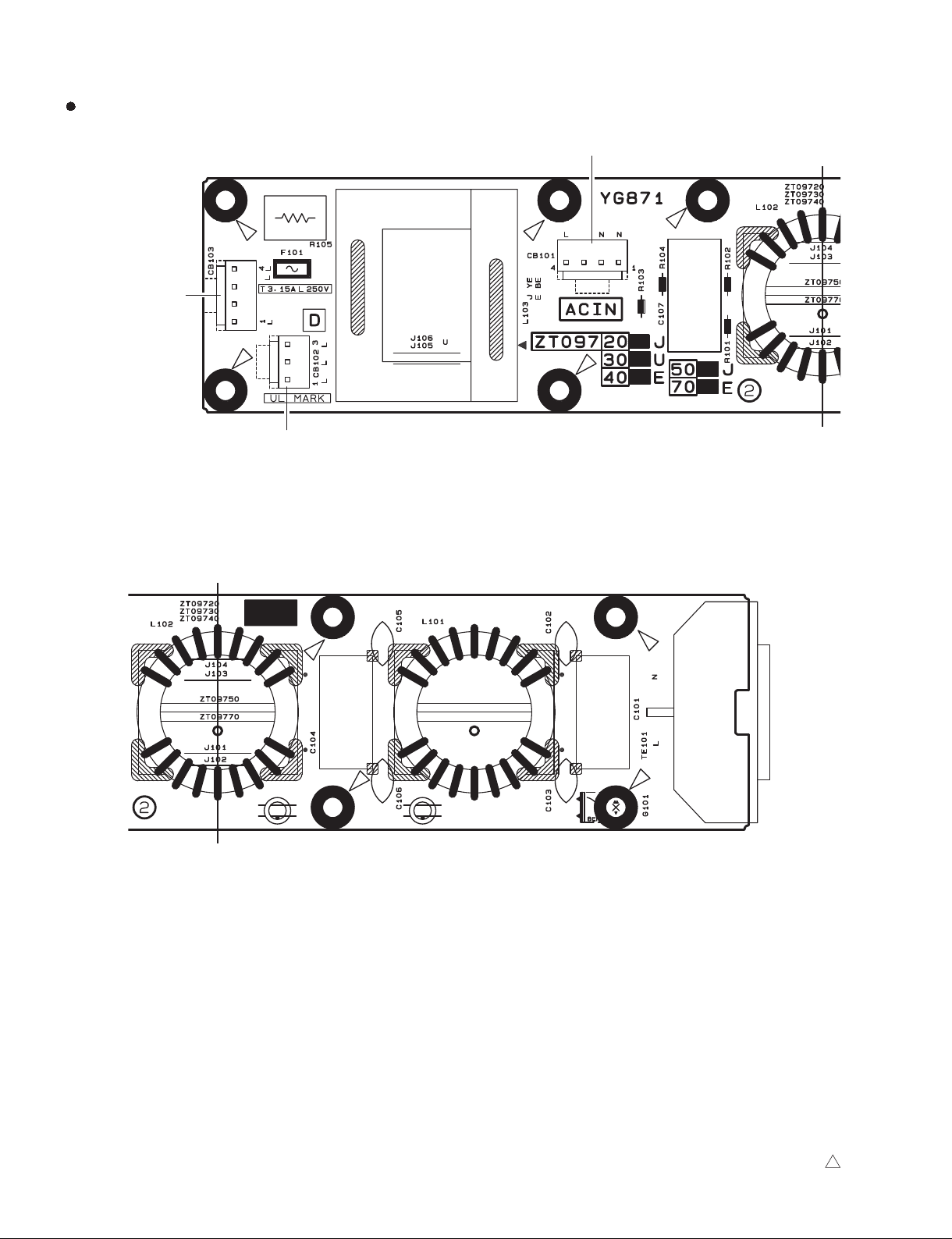
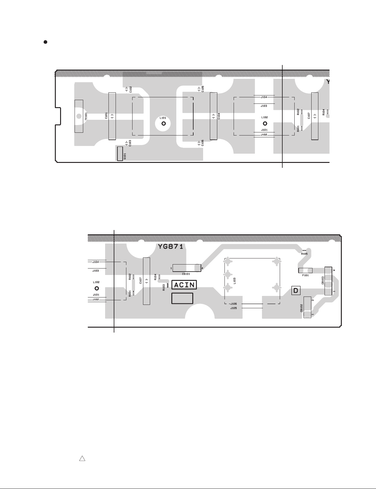
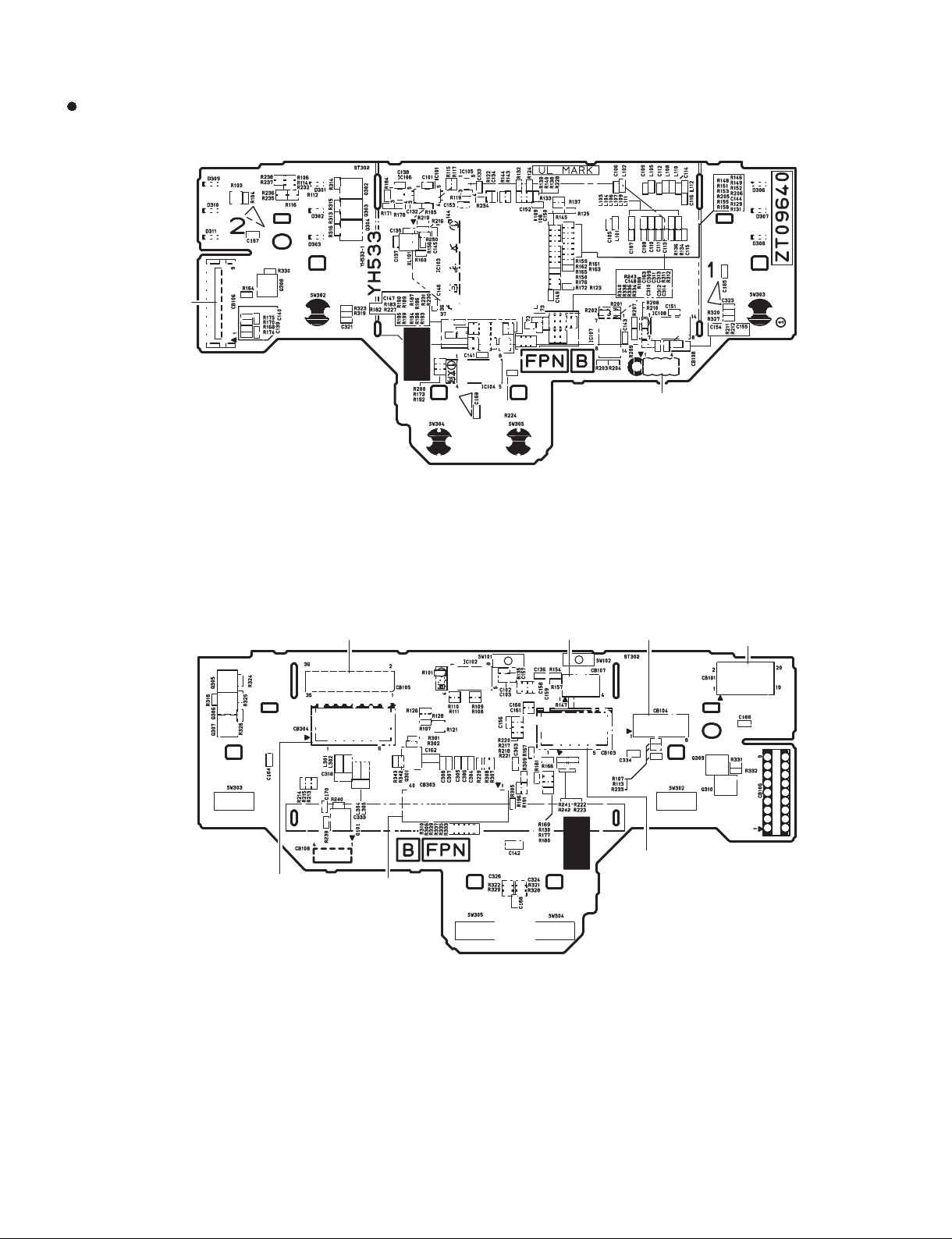
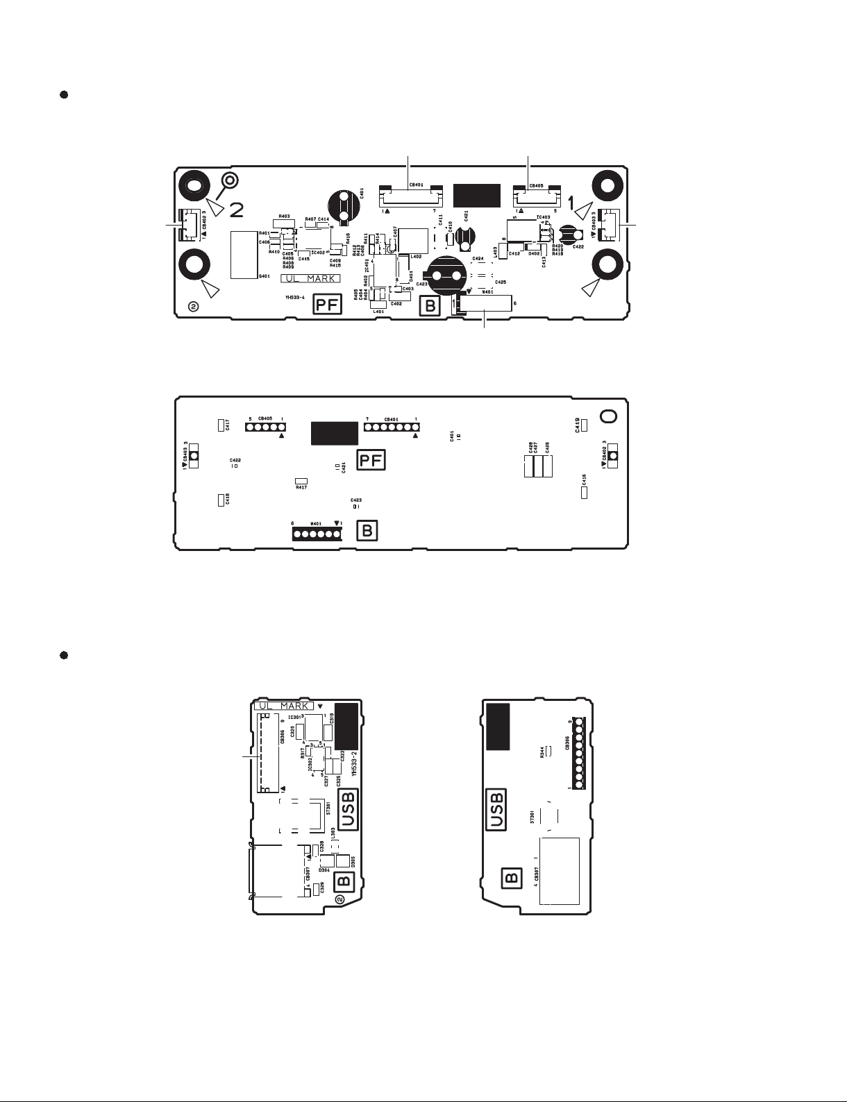
CIRCUIT BOARDS(シート基板図)
ACIN Circuit Board (YG871D0) ........................................ 22/23
AUDIO Circuit Board (YG852E0) ..................................... 24/25
ENC (PN) Circuit Board (YH533B0) ...................................... 21
FPN (PN) Circuit Board (YH533B0)....................................... 26
OUT Circuit Board (YG853E0) .............................................. 27
PF (PN) Circuit Board (YH533B0) ......................................... 30
PS Circuit Board (YG872D0) ............................................ 28/29
PSW (SUB) Circuit Board (YG978E0) ................................... 21
USB (PN) Circuit Board (YH533B0) ...................................... 30
VOL (SUB) Circuit Board (YG978E0) .................................... 31
Note: See parts list for details of circuit board component parts.
注 : シートの部品詳細はパーツリストをご参照ください。
PX10/PX8/PX5/PX3
ENC (PN) Circuit Board
to FPN-CB108
Component side
PSW (SUB) Circuit Board
POWER SW
(部品側)
Pattern side
(パターン側)
to ACIN-CB103
ENC (PN) : 2NA-ZT09640
PSW (SUB) : 2NA-ZT09940
Component side
3
(部品側)
Pattern side
(パターン側)
21
Page 22
PX10/PX8/PX5/PX3
ACIN Circuit Board
to PSW-W302A/B/C
A
to PS-CB208
to PS-CB209
A
A’
A’
AC-INLET
Component side
2NA-ZT09720
(部品側)
2
22
Page 23
ACIN Circuit Board
PX10/PX8/PX5/PX3
B
B’
B’
B
Pattern side
(パターン側)
2NA-ZT09720
2
23
Page 24
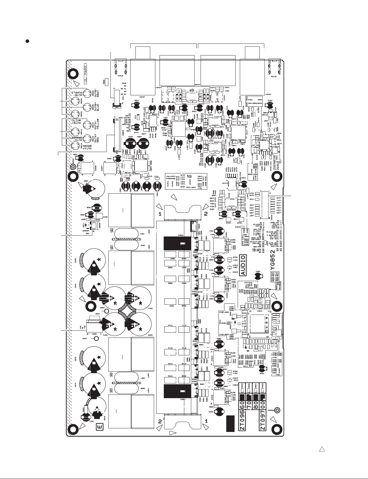
PX10/PX8/PX5/PX3
AUDIO Circuit Board
to OUT-CB901
to PS-W204to PS-W202to PS-W201A/B/C to OUT-CB902
Scale: 80/100
INPUT A INPUT B
to PF-CB405
to FPN-CB105
24
Component side
(部品側)
2NA-ZT09660
3
Page 25
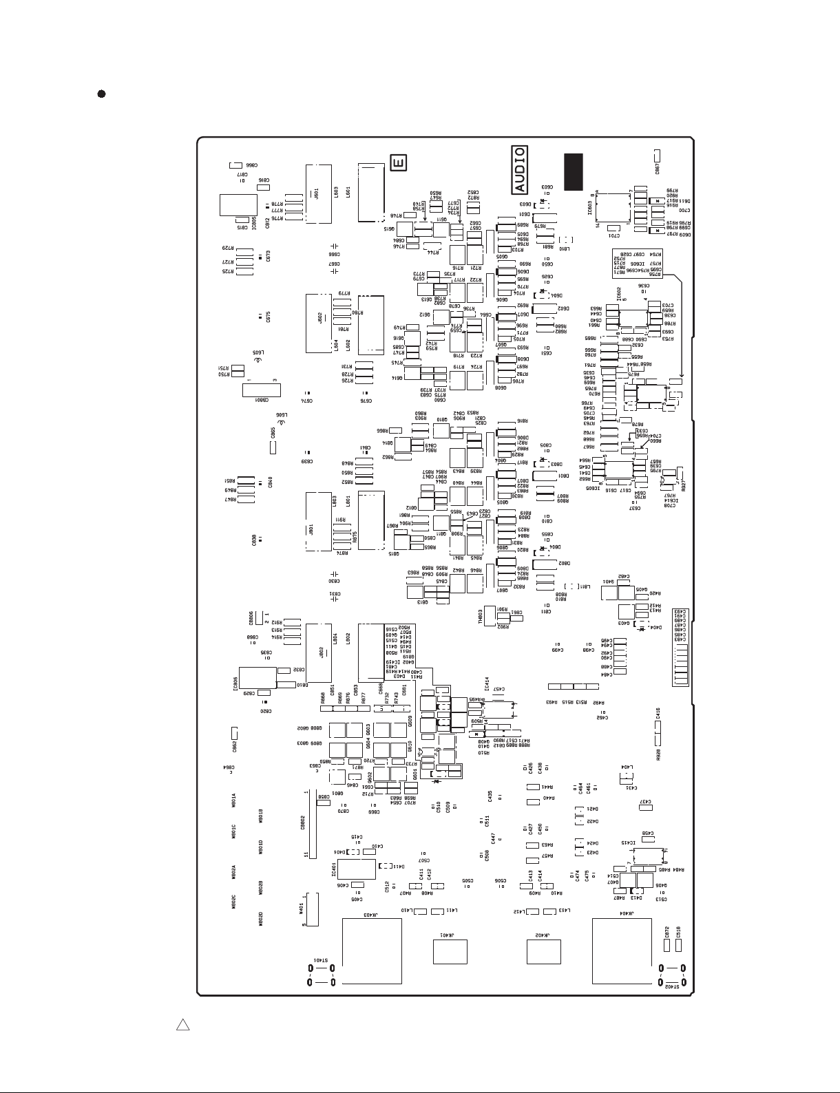
AUDIO Circuit Board
PX10/PX8/PX5/PX3
Scale: 80/100
2NA-ZT09660
Pattern side
3
(パターン側)
25
Page 26
PX10/PX8/PX5/PX3
FPN (PN) Circuit Board
to USB-CB306
to ENC-CB302
to PF-W401
to AUDIO-CB402 N.C.
to DISPLAY
N.C.
to VOL-W301
Component side
not installed
(部品側)
26
Pattern side
2NA-ZT09640
(パターン側)
Page 27
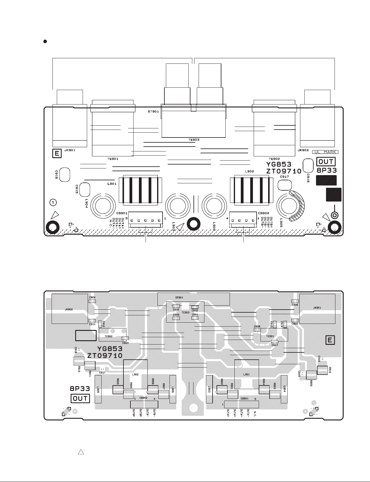
OUT Circuit Board
SPEAKERS A SPEAKERS B
PX10/PX8/PX5/PX3
to AUDIO-W801A/B/C/D to AUDIO-W802A/B/C/D
Component side
(部品側)
2NA-ZT09710
Pattern side
1
(パターン側)
27
Page 28
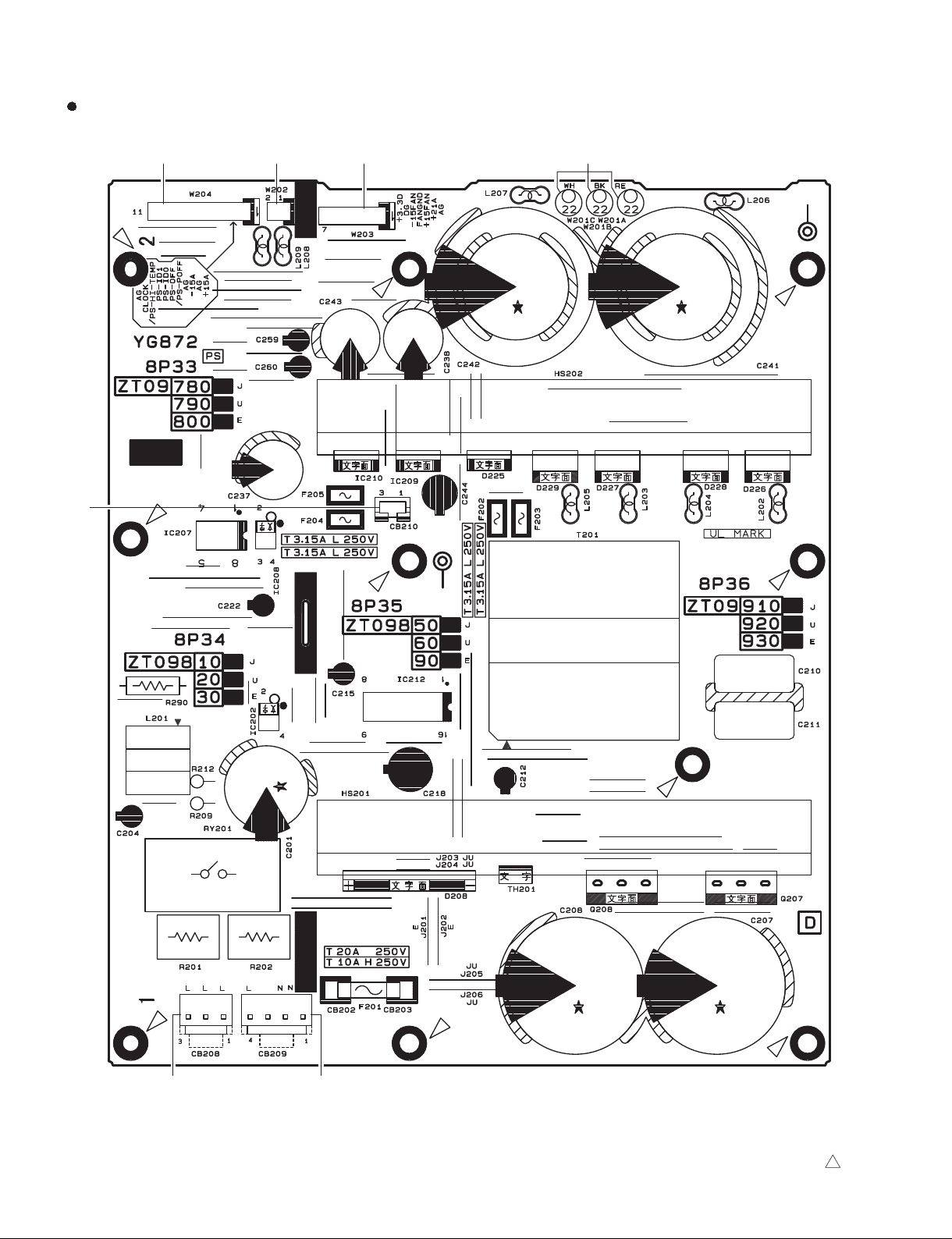
PX10/PX8/PX5/PX3
PS Circuit Board
to AUDIO-CB802 to AUDIO-CB806 to AUDIO-CB801to PF-CB401
to POWER TRANSFORMER
28
to ACIN-CB102
to ACIN-CB101
Component side
2NA-ZT09780
(部品側)
2
Page 29
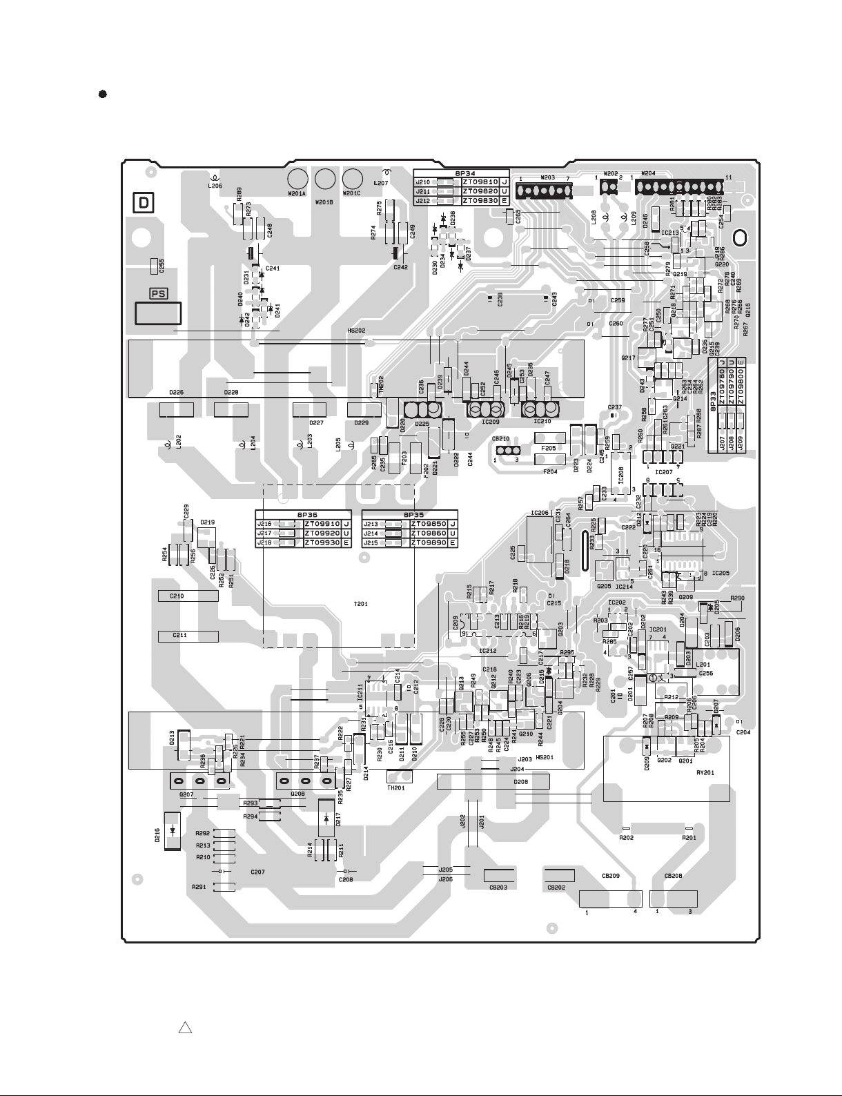
PS Circuit Board
PX10/PX8/PX5/PX3
2NA-ZT09780
Pattern side
2
(パターン側)
29
Page 30
PX10/PX8/PX5/PX3
PF (PN) Circuit Board
to PS-W203 to AUDIO-W401
to DC FAN
to FPN-CB304
to DC FAN
Component side
Pattern side
(パターン側)
(部品側)
USB (PN) Circuit Board
to FPN-CB106
30
Component side
(部品側)
Pattern side
(パターン側)
2NA-ZT09640
Page 31

VOL (SUB) Circuit Board
VOLUME A VOLUME B
PX10/PX8/PX5/PX3
to FPN-CB103
Component side
Pattern side
(パターン側)
(部品側)
2NA-ZT09940
3
31
Page 32

PX10/PX8/PX5/PX3
INSPECTION
1. Preparation
1-1. Equipment
•USB Memory
•Connect a FAT32 formatted USB2.0 memory
1-2. How to connect
Connection diagram
Insert a USB Memory in a PX's USB port.
3. List of inspection items
※○:inspect/×:not inspect
Inspection
No
category
01 USB USB Bus, USB0-ID Auto
02 Information Firmware version Measure
03 Statistics Browsing Visual
04 DP200 I2C Bus Auto
05 Temperature
Inspection item Judgment Service
VBUS Measure
/VBUS-FLG Measure
SERIES-ID Visual
AUDIO-ID Visual
AUDIO-ID Variable Semi-Auto
PS-ID0 Visual
PS-ID0 Variable Semi-Auto
PS-ID1 Visual
PS-ID1 Variable Semi-Auto
Clear Visual
OCPA Flag PROTA_N Auto
OCPB Flag PROTB_N Auto
VI-CALIB-A Auto
VI-CALIB-B Auto
V-SENSE-A (OUTVA) Auto
V-SENSE-B (OUTVB) Auto
I-SENSE-A (OUTIA) Auto
I-SENSE-B (OUTIB) Auto
/CLIP-A ON Auto
/CLIP-A OFF Auto
/CLIP-B ON Auto
/CLIP-B OFF Auto
AMP-A (OTP_PS Flag,PROT*_N)
AMP-B (T-SENSE) Auto
/HI-TEMP Auto
Auto
2. Modes for Activation
2-1. Service inspection mode
This activation mode is to perform Service inspection.
Turn on while pushing the [MENU]key, the [A]key and
the [B] key simultaneously.
[A] key [B] key
[ ] (Back) key[MENU] key Main knob
Inspection
No
category
○
×
×
○
○
○
×
○
×
○
×
○
○
○
×
×
○
○
○
○
○
○
×
×
×
×
×
○
×
06 SPI fl ash SPI Bus Auto
07 DSP I2C Bus Auto
08 Analog CFG1(+14dBu) Measure
09 LCD Parallel Bus Auto
10 FAN Turn Visual
11 LED In order Visual
12 Tact switch In order Semi-Auto
13 Rotary encoder Rotate Left Semi-Auto
Rotary potentiometer
14
15 Power off
Inspection item Judgment Service
/DSP-IRQ Auto
DSP-STATUS Auto
CFG2(+4dBu) Measure
CFG3(E-VOL=MUTE) Measure
CFG4(BOOST MODE) Measure
/DSP-MUTE ON Measure
/DSP-MUTE OFF Measure
Panel Visual
LCD-CONT (Contrast) Visual
LCD-BL (Backlight) Visual
Maximum speed Visual
Minimum speed Visual
Rotate Right Semi-Auto
VOL-ALT positive Semi-Auto
VOL-ALT negative Semi-Auto
Calibration 2 Semi-Auto
Confi rm & Save 2 Semi-Auto
/POFF-REQ /PWR-OFF(IRQ)
Visual
○
○
○
○
○
○
○
○
○
○
○
○
○
○
×
○
○
○
○
○
○
×
×
○
○
○
32
Page 33

4. Service inspection
4-1. How to connect
Refer to the “1-2. How to connect” (Page 32) of
Inspection section.
4-2. How to activate
Refer to the “2-1. Service inspection mode” (Page 32) of
Inspection section.
If powered on with service inspection mode successfully,
during Power On sequence, all LEDs light up simultaneously
for a few seconds.
4-3. The display for inspection
The PX device LCD. Category selection screen.
PX10/PX8/PX5/PX3
4-4. How to inspect
Controls Inspection category Inspection item After Execution
[MENU] key display category item display category item
[A] key select before category select before item display result before page
Switch
[B] key select next category select next item display result next page
Main knob fi x category (display item) execute item select next item
Main knob Left select before category select before item display result before page
Encoder
Main knob Right select next category select next item display result next page
Left end✽is a selecting cursor.
The automatic paging is supported.
33
Page 34

PX10/PX8/PX5/PX3
5. Inspection item
5-1. USB
5-1-1. USB Bus, USB0-ID
Contents The state of FAT32 fi le system currently recorded on
the USB memory is inspected.
Advance preparation
Confi rm the USB memory is inserted.
Service inspection screen
〈
〉
5-2. Information
5-2-1. Firmware version
Contents A version number inspects visual agreement.
Advance preparationNone.
Service inspection screen
〈
Inspect visually.
The fault location at the time of FAIL
Firmware is not upgraded correctly.
〉
The fault location at the time of FAIL
USB Bus (USB-DP, USB-DN, VBUS-EN, IC301, IC302),
USB0-ID
5-1-2. VBUS (PCB PN Assembly only)
This is not tested for service inspection of PX amplifi er.
5-1-3. /VBUS-FLG (PCB PN Assembly only)
This is not tested for service inspection of PX amplifi er.
5-2-2. SERIES-ID
Contents An SERIES-ID (from PCB PN) inspects visual
agreement.
Advance preparationNone.
Service inspection screen
〈
Inspect visually that it was displayed as “PX”.
The fault location at the time of FAIL
SERIES-ID0, SERIES-ID1, SERIES-ID2
〉
34
Page 35

PX10/PX8/PX5/PX3
5-2-3. AUDIO-ID
Contents An AUDIO-ID inspects automatically that it is in
agreement with an expected value.
Advance preparationNone.
Service inspection screen
〈
Inspect visually agreeing with the model name printed at the
panel.
The fault location at the time of FAIL
The classifi cation of PCB AUDIO connected is different.
Or, the circuit of the AUDIO-ID circumference is fault.
〉
5-2-6. PS-ID0 Variable (PCB PN Assembly only)
This is not tested for service inspection of PX amplifi er.
5-2-7. PS-ID1
Contents An PS-ID1(from PCB PS) inspects visually agreeing
with the destination of a PX amplifi er.
Advance preparationNone.
Service inspection screen
〈
Inspect visually agreeing with the destination of a PX amplifi er
using the following chart.
〉
5-2-4. AUDIO-ID Variable (PCB PN Assembly only)
This is not tested for service inspection of PX amplifi er.
5-2-5. PS-ID0
Contents An PS-ID0 (from PCB PS) inspects visually agreeing
with the model name printed at the panel.
Advance preparationNone.
Service inspection screen
〈
Inspect visually agreeing with the model name printed at the
panel.
〉
PS-ID1 destination
European model
British model
E
Korean model
Chinese model
U.S.A. model
U
Taiwan model
Brazilian model
J Japanese model
The fault location at the time of FAIL
The classifi cation of PCB PS connected is different.
Or, the circuit of the PS-ID1 circumference is fault.
5-2-8. PS-ID1 Variable (PCB PN Assembly only)
This is not tested for service inspection of PX amplifi er.
The fault location at the time of FAIL
The classifi cation of PCB PS connected is different.
Or, the circuit of the PS-ID0 circumference is fault.
35
Page 36

PX10/PX8/PX5/PX3
5-3. Statistics (Service only)
5-3-1. Browsing
Contents The operating condition statistic of amplifier is
inspected visually.
Refer to Statistics list.
Statistics list
Parameter Meaning
Power ON The number of times of turn on the power.
Encoder The number of times of rotation. Yes
Attenuator-A The number of times of rotation. Yes
Attenuator-B The number of times of rotation. Yes
Data Broken
/PS-HI-TEMP The number of /PS-HI-TEMP. Yes
Over Current
Low Temp
Low Mid Temp
High Mid Temp
High Temp
Total Op The operation total number of seconds.
Long Op
Flicker The number of power fl icker counts.
Run Away The number of run away counts.
The number of times of detecting data corruption.
The number of times that the excessive output exceeded the threshold.
The number of times of being a low temperature per unit time.
The number of times of being a lower-middle temperature per unit time.
The number of times of being a higher-middle temperature per unit time.
The number of times of being a high temperature per unit time.
The number of times that hours operated were 24 hours or more.
Clear Object
5-3-2. Clear
Contents After exchanging the following parts, a related
statistic is cleared manually.
Exchanged parts Item to clear
SW301 Rotary encoder The number of times of rotation
VR301 Rotary potentiometer The number of times of rotation
VR302 Rotary potentiometer The number of times of rotation
PCB PS The number of /PS-HI-TEMP
Advance preparationNone.
Note Don't clear accidentally.
Service inspection screen
〈
〉
Advance preparationNone.
Service inspection screen
〈
〉
Left end✽is a selecting cursor.
Left end✽is a selecting cursor.
Rotate the Main knob, confi rm the all parameters.
<Attention>
The purpose of this inspection is to obtain the hint of a fault cause.
This inspection does not pinpoint a fault location.
36
Page 37

5-4. DP200 (IC601)
5-4-1. I2C Bus
Contents Via I2C Bus which is a communication path with a
microcomputer, it inspects automatically using the
register of DP200.
Advance preparationNone.
Service inspection screen
〈
〉
PX10/PX8/PX5/PX3
5-4-4. V-SENSE (OUTVA,OUTVB)
Contents When the output voltage of amplifier without load
is normal, it inspects automatically that the value
of the OUTVA or OUTVB register of DP200 is
judgment within the range.
Advance preparation
1. Connect 8 ohms load resistances for PX amplifi er output
terminals.
2. Input 1kHz sine wave signal to PX amplifi er.
3. Adjust amplifi er outputs to 250W@8Ω.
Service inspection screen
〈
〉
Left end✽is a selecting cursor.
The fault location at the time of FAIL
I2C Bus(SCL-DP2, SCA-DP2)
5-4-2. OCPA Flag PROTA_N
This is not tested for service inspection of PX amplifi er.
5-4-3. OCPB Flag PROTB_N
This is not tested for service inspection of PX amplifi er.
Left end✽is a selecting cursor.
The fault location at the time of FAIL
VSENSEA, VSENSEB
37
Page 38

PX10/PX8/PX5/PX3
5-4-5. I-SENSE
Contents When the output current of amplifier with rated
Advance preparation
1. Connect 8 ohms load resistances for PX amplifi er output
terminals.
2. Input 1kHz sine wave signal to PX amplifi er.
3. Adjust amplifi er outputs to 250W@8Ω.
Service inspection screen
〈
(OUTIA,OUTIB)
load is normal, it inspects automatically that the
value of the OUTIA or OUTIB register of DP200 is
judgment within the range. Refer to the following
specifi cations about the normal current.
〉
5-4-9. /CLIP-B OFF
This is not tested for service inspection of PX amplifi er.
5-4-10. V-SENSE,I-SENSE Calibration
Contents This inspection is divided into every A and B, and is
performed.
When the output voltage of amplifier without load
and the output current of amplifier with rated load
are normal , the calibration of the value of the
OUTVx and OUTIx registers of DP200 are carried
out simultaneously, and each correction value is
calculated automatically. The each correction value
is saved as in the fl ash memory.
(x = A or B)
Advance preparation
1. Connect 8 ohms load resistances for PX amplifi er output
terminals.
2. Input 1kHz sine wave signal to PX amplifi er.
3. Adjust amplifi er outputs to 250W@8Ω.
Service inspection screen
〈
〉
Left end✽is a selecting cursor.
The fault location at the time of FAIL
ISENSEA, ISENSEB
5-4-6. /CLIP-A ON
This is not tested for service inspection of PX amplifi er.
5-4-7. /CLIP-A OFF
This is not tested for service inspection of PX amplifi er.
Left end✽is a selecting cursor.
The fault location at the time of FAIL
VSENSEA, VSENSEB, ISENSEA, ISENSEB
5-4-8. /CLIP-B ON
This is not tested for service inspection of PX amplifi er.
38
Page 39

PX10/PX8/PX5/PX3
5-5. Temperature
5-5-1. AMP-A (OTP_PS Flag PROT*_N)
This is not tested for service inspection of PX amplifi er.
5-5-2. AMP-B (T-SENSE)
Contents T-SENSE which is a signal which the temperature
sensor of the amplifier channel B outputs inspects
automatically whether it is in the right range.
Normal range is 240mV (5℃) - 1010mV (50℃).
Advance preparationNone.
Service inspection screen
〈
〉
5-6. SPI Flash (IC104)
5-6-1. SPI Bus
Contents Read JEDEC ID (9Fh) command is written to the
SPI Flash device for data (IC104), and it inspects
automatically that the following ID can be read.
Memory Type:40h
Capacity:14h
Advance preparationNone.
Note The inspection of the QSPI Flash device for firmware
(IC102) is omitted.
It is substituted by the check of operation of firmware
and the check of the validity at the time of firmware
upgrade.
Service inspection screen
〈
〉
Left end✽is a selecting cursor.
The fault location at the time of FAIL
Around T-SENSE signal.
5-5-3. /HI-TEMP
This is not tested for service inspection of PX amplifi er.
Left end✽is a selecting cursor.
The fault location at the time of FAIL
SPI Bus (/FLA-CS, FLA-SCK, FLA-MISO, FLA-MOSI) or
IC104 itself.
39
Page 40

PX10/PX8/PX5/PX3
5-7. DSP (IC104)
5-7-1. I2C Bus
Contents Via I2C Bus which is a communication path with a
microcomputer, it inspects automatically using the
register of DSP.
Advance preparationNone.
Service inspection screen
〈
〉
5-7-2. /DSP-IRQ
Contents The function to assert a /DSP-IRQ signal is
automatically inspected via the register of DSP.
Advance preparationNone.
Service inspection screen
〈
〉
Left end✽is a selecting cursor.
The fault location at the time of FAIL
I2C Bus (SCL-SPR, SCA-SPR)
Left end✽is a selecting cursor.
The fault location at the time of FAIL
/DSP-IRQ
40
Page 41

5-7-3. DSP-STATUS
Contents The function to monitor a DSP-STATUS signal is
automatically inspected via the register of DSP.
Advance preparationNone.
Service inspection screen
〈
〉
PX10/PX8/PX5/PX3
5-8. Analog
5-8-1. /CFG1 (+14dBu)
Contents Measure the output characteristic of ChA/ChB on
condition of the following.
PX10 PX8 PX5 PX3
Input Sensitivity +14dBu
DP200 E-VOL 0dB 0dB -2dB -3dB
NJW1194 E-VOL +6dB
Peak Limiter OFF
1/8 Power Limiter OFF
CLIP Limiter OFF
AMP Prot Gain 0dB
Slicer OFF
Regarding criteria for measurement, refer to “2-2. inspection”
(Page 54) of MEASUREMENT section.
Left end✽is a selecting cursor.
The fault location at the time of FAIL
DSP-STATUS
Advance preparationNone.
Service inspection screen
〈
〉
Left end✽is a selecting cursor.
The fault location at the time of FAIL
Around DP200 (IC601) or NJW1194 (IC422)
41
Page 42

PX10/PX8/PX5/PX3
5-8-2. CFG2 (+4dBu)
Contents Measure the output characteristic of ChA/ChB on
condition of the following.
PX10 PX8 PX5 PX3
Input Sensitivity +4dBu
DP200 E-VOL 0dB 0dB -2dB -3dB
NJW1194 E-VOL +16dB
Peak Limiter OFF
1/8 Power Limiter OFF
CLIP Limiter OFF
AMP Prot Gain 0dB
Slicer OFF
Regarding criteria for measurement, refer to “2-2. inspection”
(Page 54) of MEASUREMENT section.
Advance preparationNone.
Service inspection screen
〈
〉
5-8-3. CFG3 (Minimum volume)
Contents Measure the output characteristic of ChA/ChB on
condition of the following.
PX10 PX8 PX5 PX3
Input Sensitivity +14dBu
DP200 E-VOL MUTE
NJW1194 E-VOL -4dB
Peak Limiter OFF
1/8 Power Limiter OFF
CLIP Limiter OFF
AMP Prot Gain 0dB
Slicer OFF
Regarding criteria for measurement, refer to “2-2. inspection”
(Page 54) of MEASUREMENT section.
Advance preparationNone.
Service inspection screen
〈
〉
Left end✽is a selecting cursor.
The fault location at the time of FAIL
Around DP200 (IC601) or NJW1194 (IC422)
42
Left end✽is a selecting cursor.
The fault location at the time of FAIL
Around DP200 (IC601) or NJW1194 (IC422)
Page 43

PX10/PX8/PX5/PX3
5-8-4. CFG4 (Boost mode)
Contents Measure the output characteristic of ChA/ChB on
condition of the following.
PX10 PX8 PX5 PX3
Input Sensitivity +14dBu
DP200 E-VOL
NJW1194 E-VOL +6dB
Peak Limiter OFF
1/8 Power Limiter OFF
CLIP Limiter OFF
AMP Prot Gain 0dB
Slicer OFF
※/ AMP MUTE B signal only assert.
Regarding criteria for measurement, refer to “2-2. inspection”
(Page 54) of MEASUREMENT section.
Advance preparation
Prepare the jig for measuring an output characteristic.
Service inspection screen
〈
--- ---
〉
0dB 0dB
5-8-5. /DSP-MUTE ON
Contents Measure the output level in the state where the
/DSP-MUTE signal was asserted.
Regarding criteria for measurement, refer to “2-2. inspection”
(Page 54) of MEASUREMENT section.
Advance preparation
Prepare the jig for measuring an output characteristic.
Note The characteristic of DSP is a fl at.
Service inspection screen
〈
〉
Left end✽is a selecting cursor.
The fault location at the time of FAIL
Around DP200 (IC601) or NJW1194 (IC422)
Left end✽is a selecting cursor.
The fault location at the time of FAIL
Around /DSP-MUTE signal.
43
Page 44

PX10/PX8/PX5/PX3
5-8-6. /DSP-MUTE OFF
Contents Measure the output level in the state where the
/DSP-MUTE signal was negated.
Regarding criteria for measurement, refer to “2-2. inspection”
(Page 54) of MEASUREMENT section.
Advance preparation
Prepare the jig for measuring an output level.
Note The characteristic of DSP is a fl at.
5-9. LCD
5-9-1. Parallel Bus
Contents A parallel bus is automatically inspected by writing,
reading, comparing with the LCDC display data
RAM in the LCD module on the following two
conditions.
(1)(2)
Page address 2h 5h
Column address H 8h 8h
Column address L 0h
Data 55h
3h
AAh
Service inspection screen
〈
Left end✽is a selecting cursor.
〉
Advance preparationNone.
Note In order that comparison may use RAM besides a
viewing area, this inspection does not affect display
information.
Service inspection screen
〈
Left end✽is a selecting cursor.
〉
The fault location at the time of FAIL
Around /DSP-MUTE signal.
44
The fault location at the time of FAIL
Parallel Bus (/LCD-CS1, /LCD-RST, /LCD-RD, /LCD-WR,
LCD-A0 ~ LCD-A7) or the LCD module itself.
Page 45

PX10/PX8/PX5/PX3
5-9-2. Panel
Contents Inspect the LCD panel visually.
The following 16 patterns are displayed every 400
msec.
Seq Display Pattern Data
(1)(9)
(2)(10)
(3)(11)
(4)(12)
(5)(13)
(6)(14)
(7)(15)
(8)(16)
Advance preparationNone.
Note Thecontrast(Electronicvolume)valueistypical.
Service inspection screen
〈
Normal Solid 0000..
Normal Solid 1111..
Normal Check 0101..
Normal Check 1010..
Reverse Solid 0000..
Reverse Solid 1111..
Reverse Check 0101..
Reverse Check 1010..
〉
5-9-3. LCD-CONT (Contrast, Service Only)
Contents Inspect the LCD contrast visually.
Confirm the change of the minimum → maximum
→ center luminance visually.
Advance preparationNone.
Service inspection screen
〈
Left end✽is a selecting cursor.
〉
Left end✽is a selecting cursor.
The fault location at the time of FAIL
The LCD module.
A voltage measurement inspection is not conducted.
Inspect the lighting situation of backlight visually.
Contrast changes by pushing the Main knob.
This inspection is ended when it changes 3 times.
The fault location at the time of FAIL
LCD module
45
Page 46

PX10/PX8/PX5/PX3
5-9-4. LCD-BL (Backlight)
Contents Inspect the LCD backlight visually.
Confirm the change of the minimum → maximum
→ center luminance visually.
Advance preparationNone.
Service inspection screen
〈
〉
5-10.FAN
5-10-1. Turn (Final Assy only)
This is not tested for service inspection of PX amplifi er.
5-10-2. Maximum speed
Contents Inserviceinspectionmode:Itinspectsrotating
visually.
Advance preparationNone.
Service inspection screen
〈
〉
Left end✽is a selecting cursor.
A voltage measurement inspection is not conducted.
Inspect the lighting situation of backlight visually.
Backlight changes by pushing the Main knob.
This inspection is ended when it changes 3 times.
The fault location at the time of FAIL
LCD-BL, LCD module
Left end✽is a selecting cursor.
The fault location at the time of FAIL
Around FAN-CONT signal. FAN
46
Page 47

5-10-3. Minimum speed
Contents In service inspection mode : It inspects rotating
visually
Advance preparationNone.
Service inspection screen
〈
〉
PX10/PX8/PX5/PX3
5-11. LED
5-11-1. In order
Contents Inspect visually as follows.
1) In order of the following, observe the LED lights
up every 400msec.
2) Ovserve all LEDs light up.
3) Ovserve all LEDs light down.
Advance preparationNone.
Service inspection screen
〈
〉
Left end✽is a selecting cursor.
The fault location at the time of FAIL
Around FAN-CONT signal. FAN
Inspect visually.
The fault location at the time of FAIL
POW-LD, ALRT-LD, USB-LD,
PROTA-LD, LIMA-LD, SIGA-LD
PROTB-LD, LIMB-LD, SIGB-LD
D309, D310, D311,
D301, D302, D303,
D306, D307, D308
47
Page 48

PX10/PX8/PX5/PX3
5-12.Tact switch
5-12-1. In order
Contents According to directions of a screen, a semiautomatic
inspection is conducted by pushing fi ve switches in
following order.
It is failure, when the switch which should be pushed
on the next is not displayed after pushing a switch, or
when the switch which should be pushed on the next is
displayed, although a switch is not pushed.
Advance preparationNone.
The fault location at the time of FAIL
/SELA-SW, /MENU-SW, /BACK -SW, /ENC-SW,
/SELB-SW
SW302, SW304, SW305, SW301, SW303
Service inspection screen
〈
〉
48
Page 49

5-13.Rotary encoder
5-13-1. Rotate Left
Contents A semiautomatic inspection is conducted by turning
a rotary encoder to the three lefts (counterclockwise
rotation).
When a rotating left cannot be detected, it judges
with it being failure.
PX10/PX8/PX5/PX3
5-13-2. Rotate Left
Contents A semiautomatic inspection is conducted by turning
a rotary encoder to the three rights (clockwise
rotation).
When a rotating right cannot be detected, it judges
with it being failure.
Advance preparationNone.
Service inspection screen
〈
Left end✽is a selecting cursor.
〉
Advance preparationNone.
Service inspection screen
〈
Left end✽is a selecting cursor.
〉
The fault location at the time of FAIL
ENC-A, ENC-B
SW301
The fault location at the time of FAIL
ENC-A, ENC-B
SW301
49
Page 50

PX10/PX8/PX5/PX3
5-14. Rotary potentiometer
5-14-1. VOL-ALT positive
This is not tested for service inspection of PX amplifi er.
5-14-2.VOL-ALT negative
This is not tested for service inspection of PX amplifi er.
5-14-3.Calibration 2
Contents The voltage for every click of all rotary potentiometer
with large variation is acquired.
Advance preparation
The index of both rotary potentiometer A/B is adjusted in the
maximum position.
3) If SIGNAL LED of both A/B lights up, it means that voltage
acquisition of this position was completed.
2) 3) is repeated in order to acquire the voltage of the next click position.
4) It will end, if the index of a variable resister arrives at the
minimum position.
An end can be checked because SIGNAL LED lights down.
1) A start of execution will light up SIGNAL LED of both A/B.
SIGNAL LED means “permitting rotation”.
2) The rotary potentiometer of both A/B is turned to the left
(1 click, counterclockwise rotation).
CLIP/LIMIT LED of both A/B lights up.
CLIP/LIMIT LED means “under voltage acquisition”,
“prohibiting rotation”.
Don't rotate the rotary potentiometer.
Note If you have turned 2 or more clicks at once, at this time,
an error will not be displayed but will be ended normally.
(an error will display in 5-14-4. Confi rm & Save 2.)
If there is consciousness that you have turned 2 or more clicks at
once, you should retry operation independently
When retry operation, the [BACK] switch is pushed and canceled
once again. And it returns to a maximum position and retry
from 1).
50
Page 51

When a [BACK] switch is pushed:
When it returns to a maximum position:
The voltage value for every click is not saved within this
inspection, only held temporarily.
The voltage value is collectively saved in 5-14-4. Confi rm & Save 2.
If it does not end even if you turn correctly, it will be failure of a
rotary potentiometer.
PX10/PX8/PX5/PX3
The fault location at the time of FAIL
VR301, VR302
5-14-4.Confirm & Save 2
Contents In “5-14-3. Calibration 2”, it is inspected semi-
automatically whether the voltage value read for
every click is right.
If the voltage value for every click is right, it saves
in the fl ash memory.
Advance preparation
“5-14-3. Calibration 2” had been fi nished.
The index of the rotary potentiometer of both A/B is aligned
with the maximum position as follows.
Service inspection screen
〈
Left end✽is a selecting cursor.
〉
1) If the voltage value for every click is right, a start of execution
will light up SIGNAL LED of both A/B.
SIGNAL LED means “permitting rotation”.
51
Page 52

PX10/PX8/PX5/PX3
2) The index of the rotary potentiometer of both A/B is aligned
with the minimum position as follows.
It will end, if the both SIGNAL LED lights up.
The voltage value for every click saves in the fl ash memory.
Service inspection screen
〈
〉
5-15 Power off
Contents Inspect the shutdown of the power supply when
POFF-REQ is activated.
At this time, it also checks that /PWR-OFF occurs
automatically.
Advance preparationNone.
Note In Final Assy or Service inspection, A power supply is
shut down while the power switch has been an ON state.
You need to turn off a power switch manually, after
ending an inspection visually.
It is set to “FAIL” when there is no response, even if
PWR-OFF becomes temporary standard time.
Service inspection screen
〈
〉
Left end✽is a selecting cursor.
The fault location at the time of FAIL
Around /POFF-REQ, POFF-REQ.
The fault location at the time of FAIL
This is not failure. This cause was not successful when you
performed calibration.
It is necessary to retry “5-14-3. Calibration 2”.
52
Page 53

MEASUREMENT
1. Measurement condition
PX10/PX8/PX5/PX3
1-1. Environment
Normal temperature: 5 to 40 degrees
Normal humidity: 30 to 90%
Note) [the following measurement conditions are
permitted if measurement result is in the inspection
standard. (Temperature: 5 to 40 degrees, Humidity: 20
to 90%) But measure it again at the normal temperature
and normal humidity when it varies from the inspecting
standard.]
1-2. Power Source
Destination Voltage Frequency
J 100V +2/-0% 50Hz
U/T/BRA 120V +2/-0% 60Hz
E/B/K/CHN 230V +2/-0% 50Hz
1-3. Measuring instruments
The measuring instruments shall have enough accuracy
and precision to measure the specifications of each
characteristic to be inspected.
The input impedance of the measuring instruments shall be
100kohms or more.
Use the measuring instrument that can measure the
specifi cation value described in this specifi cation.
1-4. Caution for measurement environment
Connected chart when classD amplifi er (PX amplifi er) is
measure
Insert AUX-0025 between classD amplifi er and the audio
analyzer when you measure classD amplifi er.
1-3-1. Input terminals
The XLR and PHONE-JACK are used to connect input
signals. It shall be a balanced input.
A XLR terminal performs measurement without
directions.
1-3-2. Output terminals
The SPEAKON, PHONE-JACK and 5WAY terminal are
used to connect output loads.
A SPEAKON terminal performs measurement without
directions.
1-3-3. Filter for measurement
Use AUX-0025 Filter for the measurement of 2-2-1. Gain
to 2-2-14. Maximum Output (BOOST Mode).
Use the low-pass filter of 20kHz according to the
measurement item.
1-3-4. Connection
Refer to the “1-2. How to connect” (Page 32) of INSPECTION
section.
Reason why insertion of AUX-0025 is indispensable
The high frequency noise caused by the switching drive is
included in the output signal of classD amplifi er.
However, the audio analyzer doesn't generally assume
the high frequency. In a word, there is no tolerance to the
high frequency.
Therefore, there is a possibility that the audio analyzer
doesn't operate normally when the high frequency is not
removed with AUX-0025.
The reason to recommend the above-mentioned
connection method
Figure 2 is the block diagram of the output composition
of the PX amplifi er.
The output of classD amplifi er is not necessarily limited
the shingle-end output.
Moreover, it is possible to understand that reversing of the
phase by HOT and COLD from the block diagram.
The output method of a recent classD amplifier takes
various forms like this.
53
Page 54

PX10/PX8/PX5/PX3
Therefore, the connection method with the interchangeability
that can correspond to any amplifier output method is
preferable. The above-mentioned connection
method can be compatible for the amplifier output with
the single end output and the bridge output, and apply any
audio analyzer.
Please shorten between the amplifi er to be measured and
the analyzer to suppress the infl uence of turbulence and
connect it. Moreover, please make to fl oating
without fail for the output.
(One on the load side is not grounded. When monitoring
with the oscilloscope, it does based on the chassis
playground. )
2. Electric characteristics
2-1. Preparation
2-1-1. Load resistances
The load resistances for each output terminals are as follows.
8Ω MODE:8ohms±1% (Rated 750W or more)
2Ω MODE:2ohms±1% (Rated 250W or more)
FlowofsignalandoutputmethodofPXamplifier
〈Fig. 2〉
In PX amplifi er, the type of output is the BTL fi xation. (Fig. 2)
2-1-2. Input Signal
Unless otherwise specifi ed, the input signal should be 1kHz sine wave.
The input signal impedance should be 100〜150 ohms.
0dBu is referenced to 0.775Vrms.
2-2. Inspection
2-2-1. Gain
Measurement condition Criteria
Select “Analog > CFG1(+14dBu)” with Service inspection mode.
Measured mode/8Ω MODE
The sine wave of 1kHz -6dBu is input to the input terminal,
and the output level of SP OUT is measured.
Select “Analog > CFG2(+4dBu)” with Service inspection mode.
Measured mode/8Ω MODE
The sine wave of 1Hz -6dBu is input to the input terminal,
and the output level of SP OUT is measured.
All channel
PX10 21.3dBu ± 2dB
PX8 20.3dBu ± 2dB
PX5 18.3dBu ± 2dB
PX3 16.1dBu ± 2dB
Between channel
± 2dB
All channel
PX10 31.3dBu ± 2dB
PX8 30.3dBu ± 2dB
PX5 28.3dBu ± 2dB
PX3 26.1dBu ± 2dB
Between channel
± 2dB
54
Page 55

2-2-2. Frequency Response
Measurement condition Criteria
PX10/PX8/PX5/PX3
Select “Analog > CFG1(+14dBu)” with Service inspection mode.
Measured mode/8Ω MODE
The sine wave of 1kHz, -11dBu is input to the input terminal,
and the output level of SP OUT is measured.
The sine wave of 20Hz, -11dBu is input to the input terminal,
and the output level of SP OUT is measured.
The sine wave of 20kHz -11dBu is input to the input terminal,
and the output level of SP OUT is measured.
2-2-3. Total Harmonics Distortion
Measurement condition Criteria
Select “Analog > CFG1(+14dBu)” with Service inspection mode.
Measured mode/8Ω MODE
When the sine wave of 1kHz is input to the input terminal, and the following
table outputs are obtained, total harmonics distortion is measured.
PX10 500W 38.3dBu ② PX10 10W 21.3dBu
①
PX8 400W 37.3dBu PX8 10W 21.3dBu
PX5 250W 35.3dBu PX5 10W 21.3dBu
PX3 150W 33.0dBu PX3 10W 21.3dBu
(half power) (10W)
Measurements are recorded as (A1).
The range of 0±1dB based on A1.
The range of 0±1dB based on A1.
All channel
THD=0.3% or less.
①
THD=0.1% or less.
②
※Use the low-pass fi lter of 20kHz for the measurement.
※Drive all channels.
2-2-4. Residual noise level
Measurement condition Criteria
Select “Analog > CFG3(E-VolMute)” with Service inspection mode.
Measured mode/8Ω MODE
The inputs of both Ach/Bch are terminated by 100〜150ohm resistor.
※Use the low-pass fi lter of 20kHz for the measurement.
All channel
PX10 -58dBu or less
PX8 -58dBu or less
PX5 -58dBu or less
PX3 -59dBu or less
55
Page 56

PX10/PX8/PX5/PX3
2-2-5. DSP-MUTE noise level
Measurement condition Criteria
Select “Analog > CFG1(+14dBu)” with Service inspection mode.
Measured mode/8Ω MODE
The signal of -10dBu is input to input terminal.
Select “Analog > DSP-MUTE ON ” with Service inspection mode.
※Use the low-pass fi lter of 20kHz for the measurement.
※Item /DSP-MUTE OFF is executed, after ending an inspection.
2-2-6. Output noise level
Measurement condition Criteria
Select “Analog > CFG1(+14dBu)” with Service inspection mode.
Measured mode/8Ω MODE
The inputs of both Ach/Bch are terminated by 100〜150ohm resistor.
※Use the low-pass fi lter of 20kHz for the measurement.
2-2-7. Crosstalk
All channel
PX10 -52dBu or less
PX8 -53dBu or less
PX5 -54dBu or less
PX3 -55dBu or less
All channel
PX10 -54dBu or less
PX8 -55dBu or less
PX5 -56dBu or less
PX3 -57dBu or less
Measurement condition Criteria
Select “Analog > CFG1(+14dBu)” with Service inspection mode.
Measured mode/8Ω MODE
1kHz signal applied to Ach input terminal and adjust the signal level the Ach output
level is to be as below. And Bch input terminal shall be terminated with 100
150ohm resistor. Measure the voltage of Bch output terminal.
PX10 500W 38.3dBu
PX8 400W 37.3dBu
PX5 250W 35.3dBu
PX3 150W 33.0dBu
※Use the low-pass fi lter of 20kHz for the measurement.
All channel
PX10 -21.7dBu or less
PX8 -22.7dBu or less
PX5 -24.7dBu or less
PX3 -27.0dBu or less
〜
56
Page 57

2-2-8. DP200 V-SENSE,I-SENSE Calibration
Measurement condition Criteria
PX10/PX8/PX5/PX3
Select “Analog > CFG1(+14dBu)” with Service inspection mode.
Measured mode/8Ω MODE
Amplifi er outputs are adjusted to 250W@8Ω
Select “Analog > DP200 > V&I Calib-A, DP200 > V&I Calib-B” with Service
inspection mode.
※ Drive each channel.
2-2-9. Confirmation of DP200 V-SENSE
Measurement condition Criteria
Select “Analog > CFG1(+14dBu)” with Service inspection mode.
Measured mode/8Ω MODE
Amplifi er outputs are adjusted to 250W@8Ω
Select “Analog > DP200 > V-SENSE-A, DP200 > V-SENSE-B” with Service
inspection mode.
※Drive each channel.
The test program judge ‘PASS’ or ‘FAIL’ automatically.
When the calibration is completed successfully, it is
※
outputted as PASS.
The test program judge ‘PASS’ or ‘FAIL’ automatically.
2-2-10. Confirmation of DP200 I-SENSE
Measurement condition Criteria
Select “Analog > CFG1(+14dBu)” with Service inspection mode.
Measured mode/8Ω MODE
Amplifi er outputs are adjusted to 250W@8Ω
Select “Analog > DP200 > I-SENSE-A, DP200 > I-SENSE-B” with Service
inspection mode.
※Drive each channel.
2-2-11. Maximum Output 1 (STEREO Mode
) (
8Ω Mode /All channels drive
Measurement condition Criteria
Select “Analog > CFG1(+14dBu)” with Service inspection mode.
Measured mode/8Ω MODE
Refer to the “Setups at the time of maximum output measurement”(Page 59).
The test program judge ‘PASS’ or ‘FAIL’ automatically.
)
All channel
PX10 More than 243Vp-p
PX8 More than 227Vp-p
PX5 More than 179Vp-p
PX3 More than 139Vp-p
※Drive all channels.
57
Page 58

PX10/PX8/PX5/PX3
2-2-12. Maximum Output (STEREO Mode
) (
8Ω Mode/1 channel drive
Measurement condition Criteria
Select “Analog > CFG1(+14dBu)” with Service inspection mode.
Measured mode/8Ω MODE
Refer to the “Setups at the time of maximum output measurement”(Page 59).
※Driveeachchannel.
2-2-13. Maximum Output (STEREO Mode
) (
2Ω Mode/1 channel drive
Measurement condition Criteria
Select “Analog > CFG1(+14dBu)” with Service inspection mode.
Measured mode/2Ω MODE
Refer to the “Setups at the time of maximum output measurement”(Page 59).
)
All channel
PX10 More than 253Vp-p
PX8 More than 227Vp-p
PX5 More than 179Vp-p
PX3 More than 139Vp-p
)
All channel
PX10 More than 105.9Vp-p
PX8 More than 98.0Vp-p
PX5 More than 89.5Vp-p
PX3 More than 69.3Vp-p
※Driveeachchannel.
2-2-14. Maximum Output (BOOST Mode
) <
PX5, PX3 only
Measurement condition Criteria
Select “Analog > CFG4(BoostMode)” with Service inspection mode.
Measured mode/8Ω MODE
Refer to the “Setups at the time of maximum output measurement”(Page 59).
>
A channel only
PX5 More than 226.3Vp-p
PX3 More than 196.0Vp-p
58
Page 59

PX10/PX8/PX5/PX3
Setups at the time of maximum output measurement
This item shall be tested with each measurement condition load resistances for each output terminals.
The burst signal described in the following fi gure is applied to each input terminals.
The peak-to-peak voltage of the last one wave of output burst signal (Vburst) should become a judgment value of a criterion.
When the shape of waves is read with an oscilloscope, the center of the emission line shall be adopted as the measurement value.
Each channel shall be tested at alone.
500mSec
Vburst
1mSec
Close-up
20mSec
The center of the emission line shall
be adopted as the measurement value.
The last one wave of burst signal
shall be measured.
Siganal
Cursor
(
Reference
)
This item is to test the output ability of the power amplifi er. Please calculate from the gain of each channel and set an appropriate input
level.
In consideration of the accuracy of the signal generator and the measuring instrument, an input level that is about 0.5% higher than the
level with which the output of the lowest judgment value is expected is recommended.
3. Settings after the inspection has done
•Rotary potentiometers are adjusted the left end.
•A power switch is turned off."
59
Page 60

PX10/PX8/PX5/PX3
UPDATAING FIRMWARE
1. Preparation
1-1. Equipment
•USB Memory(FAT32 or FAT16 format)
※Copythefirmwarefile(PXPROG.BIN)tothe
rootdirectoryoftheUSBmemory.
1-2. How to connect
Connectiondiagram
Refertothe1-2.Howto connect (Page 32) of
Inspectionsection.
1-3. Updating procedure
1) Turn off the power supply of PX amplifi er.
(Or check that PX amplifi er is a power OFF state.)
2) USB memory in PX amplifi er.
3) Turn on the power supply of PX amplifi er.
4) LCD is displayed as follows.
1-4. Attention
You must not turn off the power supply of PX amplifier
until update is completed.
When you turn on the power supply of PX amplifier on
condition of the following, it does not change in update
mode.
At this time, PX amplifi er is started by the normal mode.
(An error is not displayed at this time.)
• The USB memory is not inserted in PX amplifi er.
• The USB memory has broken.
• The USB memory is not formatted in FAT32 or FAT16.
• In a USB memory, the normal update file for PX
amplifi ers is not found.
5) If you want to stop update, press keys other than the
Main knob.
6) Push the Main knob, if you want to start update.
Update is started. Wait until it ends.
% means progression.
60
Page 61

検査
PX10/PX8/PX5/PX3
1. 準備
1-1. 機材
•USBメモリー
•FAT32フォーマットされたUSB2.0メモリー
1-2. 接続方法
接続図
USBメモリーをパネル上のUSBポートに差します。
3. 検査項目一覧
※○:検査する/×:検査しない
2. 起動モード
2-1. サービス検査モード
このモードは、サービス検査用です。
[MENU]キー、[A]キー、[B]キーを同時に押した状態で
電源を入れます。
[A]キー [B]キー
[MENU]キー メインノブ
[ ]
(バック)キー
No 検査カテゴリ 検査項目 判定 サービス
01 USB USB Bus, USB0-ID
VBUS
/VBUS-FLG
02 Information Firmware version
SERIES-ID
AUDIO-ID
AUDIO-ID Variable
PS-ID0
PS-ID0 Variable
PS-ID1
PS-ID1 Variable
03 Statistics Browsing
Clear
04 DP200 I2C Bus
OCPA Flag PROTA_N
OCPB Flag PROTB_N
VI-CALIB-A
VI-CALIB-B
V-SENSE-A (OUTVA)
V-SENSE-B (OUTVB)
I-SENSE-A (OUTIA)
I-SENSE-B (OUTIB)
/CLIP-A ON
/CLIP-A OFF
/CLIP-B ON
/CLIP-B OFF
05 Temperature
AMP-A (OTP_PS Flag,PROT*_N)
AMP-B (T-SENSE)
/HI-TEMP
自動 ○
測定 ×
測定 ×
測定 ○
目視 ○
目視 ○
半自動 ×
目視 ○
半自動 ×
目視 ○
半自動 ×
目視 ○
目視 ○
自動 ○
自動 ×
自動 ×
自動 ○
自動 ○
自動 ○
自動 ○
自動 ○
自動 ○
自動 ×
自動 ×
自動 ×
自動 ×
自動 ×
自動 ○
自動 ×
No 検査カテゴリ 検査項目 判定 サービス
06 SPI fl ash SPI Bus
07 DSP I2C Bus
/DSP-IRQ
DSP-STATUS
08 Analog CFG1(+14dBu)
CFG2(+4dBu)
CFG3(E-VOL=MUTE)
CFG4(BOOST MODE)
/DSP-MUTE ON
/DSP-MUTE OFF
09 LCD Parallel Bus
Panel
LCD-CONT (Contrast)
LCD-BL (Backlight)
10 FAN Turn
Maximum speed
Minimum speed
11 LED In order
12 Tact switch In order
13 Rotary encoder Rotate Left
Rotate Right
Rotary potentiometer
14
15 Power off
VOL-ALT positive
VOL-ALT negative
Calibration 2
Confi rm & Save 2
/POFF-REQ /PWR-OFF(IRQ)
自動 ○
自動 ○
自動 ○
自動 ○
測定 ○
測定 ○
測定 ○
測定 ○
測定 ○
測定 ○
自動 ○
目視 ○
目視 ○
目視 ○
目視 ×
目視 ○
目視 ○
目視 ○
半自動 ○
半自動 ○
半自動 ○
半自動 ×
半自動 ×
半自動 ○
半自動 ○
目視 ○
61
Page 62

PX10/PX8/PX5/PX3
4. サービス検査
4-1. 接続方法
検査の「1-2.接続方法」(61ページ)を参照してくださ
い。
4-2. 起動方法
検査の「2-1.サービス検査モード」(61ページ)を参 照してく
ださい 。
サービス検査モードに 移 行 すると、すべてのLEDが数秒間
同時に点灯します。
4-3. 検査画面
本体LCD。カテゴリ選択画面。
4-4. 検査方法
操作子 検査カテゴリ 操作項目 実行後
スイッチ
エンコーダー
左端の✽は、選択カーソルです。
自動ページングに対応しています。
[MENU]キー カテゴリ項目表示 カテゴリ項目表示
[A]キー 前のカテゴリ選択 前の検査選択 検査結果前ページ
[B]キー 次のカテゴリ選択 次の検査選択 検査結果次ページ
メインノブ カテゴリ確定(検査項目表示) 検査実行 次の検査選択
メインノブ左 前のカテゴリ選択 前の検査選択 検査結果前ページ
メインノブ右 次のカテゴリ選択 次の検査選択 検査結果次ページ
62
Page 63

5. 検査項目
PX10/PX8/PX5/PX3
5-1. USB
5-1-1.USBBus,USB0-ID
内容 USBメモリーに記録されているFAT32ファイルシ
ステムの状態を検査します。
事前準備 USBメモリーが装着されていることを確認しま
す。
〈サービス検査画面〉
5-2. Information
5-2-1.Firmwareversion
内容 ファームウェアバージョンの目視検査をします。
事前準備 なし。
〈サービス検査画面〉
目視確認します。
FAIL時の故障個所
ファームウェアが正しくバージョンアップされていま
せん。
FAIL時の故障個所
USBBus(USB-DP,USB-DN,VBUS-EN, IC301,
IC302),USB0-ID
5-1-2.VBUS(PCBPNAssyonly)
サービス検査では実施しません。
5-1-3./VBUS-FLG(PCBPNAssyonly)
サービス検査では実施しません。
5-2-2.SERIES-ID
内容 PCBPNからのSERIES-IDを目視検査します。
事前準備 なし。
〈サービス検査画面〉
「PX」と表示されることを目視検査します。
FAIL時の故障個所
SERIES-ID0,SERIES-ID1,SERIES-ID2
63
Page 64

PX10/PX8/PX5/PX3
5-2-3.AUDIO-ID
内容 PCBAUDIOからのAUDIO-IDと、期待値との合致を
自動検査します。
事前準備 なし。
〈サービス検査画面〉
パネル印刷されたモデル名と合致するか、
目視確認します。
FAIL時の故障個所
接続されているPCBAUDIOの種別が違います。
または、AUDIO-ID周辺回路の故障です。
5-2-6.PS-ID0Variable(PCBPNAssyonly)
サービス検査では実施しません。
5-2-7.PS-ID1
内容 PCBPSからのPS-ID1と、PX本体の仕向けとの合致
を目視します。
事前準備 なし。
〈サービス検査画面〉
以下の表を使用して、PX本体の仕向けと合致するか目視確
認します。
5-2-4.AUDIO-IDVariable(PCBPNAssyonly)
サービス検査では実施しません。
5-2-5.PS-ID0
内容 PCB PSからのPS-ID0とパネル印刷されたモデル
名との合致を目視します。
事前準備 なし。
〈サービス検査画面〉
パネル印刷されたモデル名と合致するか、
目視確認します。
PS-ID1 仕向け
Europeanmodel
Britishmodel
E
Koreanmodel
Chinesemodel
U.S.A.model
U
Taiwanmodel
Brazilianmodel
J Japanesemodel
FAIL時の故障個所
接続されているPCBPSの種別が違います。
または、PS-ID1周辺回路の故障です。
5-2-8.PS-ID1Variable(PCBPNAssyonly)
サービス検査では実施しません。
FAIL時の故障個所
接続されているPCBPSの種別が違います。
または、PS-ID0周辺回路の故障です。
64
Page 65

5-3. 統計(サービス検査専用)
5-3-1.Browsing
内容 アンプの使用状況統計値を、目視で確認します。
統計値一覧を参照します。
PX10/PX8/PX5/PX3
5-3-2.Clear
内容 以下の部品交換に伴い、関連する統計値を手動でク
リアします。
統計値一覧
パラメータ 意味 クリア対象
PowerON 電源オン回数
Encoder 回転回数 Yes
Attenuator-A 回転回数 Yes
Attenuator-B 回転回数 Yes
DataBroken データ破壊検出回数
/PS-HI-TEMP /PS-HI-TEMP回数 Yes
OverCurrent
LowTemp 単位時間あたりの、低温回数
LowMidTemp
HighMidTemp
HighTemp 単位時間あたりの、高温回数
TotalOp 稼働総秒数
LongOp
Flicker 電源瞬断が起きた回数
RunAway 暴走が起きた回数
過大な出力が、閾値を超えた回数
単位時間あたりの、低〜中温度回数
単位時間あたりの、中〜高温度回数
稼働時間が、24時間以上だった回数
事前準備 なし。
〈サービス検査画面〉
交換部品 クリア対象
SW301 Rotaryencoder 回転回数
VR301 Rotarypotentiometer 回転回数
VR302 Rotarypotentiometer 回転回数
PCBPS /PS-HI-TEMP回数
事前準備 なし。
注意事項 誤ってクリアしないでください。
〈サービス検査画面〉
左端の✽は、選択カーソルです。
メインノブを回してすべてのパラメータを確認します。
【注意】
この検査の目的は、故障原因のヒントを得ることにあり
ます。
故障個所を特定するものではありません。
左端の✽は、選択カーソルです。
65
Page 66

PX10/PX8/PX5/PX3
5-4. DP200(IC601)
5-4-1.I2CBus
内容 マイコンとの通信経路であるI2Cバス経由で、DP200
のレジスタを用い自動検査します。
事前準備 なし。
5-4-4.V-SENSE(OUTVA,OUTVB)
内容 無負荷アンプ出力が規定電圧を出力している状態に
おいて、DP200のOUTVAレジスタ及びOUTVBレジ
スタの値が判定範囲内であることを自動検査しま
す。
〈サービス検査画面〉
左端の✽は、選択カーソルです。
事前準備 1. PXアンプの出力端子に8Ωのダミー抵抗を接
続します。
2.正弦波1kHzをPXアンプの入力端子に入力し
ます。
3.アンプ出力を250W@8Ωに調整します。
〈サービス検査画面〉
左端の✽は、選択カーソルです。
FAIL時の故障個所
I2CBus(SCL-DP2,SCA-DP2)
5-4-2.OCPAFlagPROTAN
サービス検査では実施しません。
5-4-3.OCPBFlagPROTBN
サービス検査では実施しません。
66
FAIL時の故障個所
VSENSEA,VSENSEB
Page 67

PX10/PX8/PX5/PX3
5-4-5.I-SENSE(OUTIA,OUTIB)
内容 定格負荷アンプ出力が規定電流を出力している状態
において、DP200のOUTIAレジスタ及びOUTIBレ
ジスタの値が判定範囲内であることを自動検査しま
す。
事前準備 1. PXアンプの出力端子に8Ωのダミー抵抗を接
続します。
2.正弦波1kHzをPXアンプの入力端子に入力し
ます。
3.アンプ出力を250W@8Ωに調整します。
〈サービス検査画面〉
左端の✽は、選択カーソルです。
5-4-10.V-SENSE,I-SENSECalibration
内容 この検査は、A、Bごとに分けて、実行します。
無負荷アンプ出力が規定電圧を出力し、定格負荷ア
ンプ出力が規定電流を出力している状態において、
DP200のOUTVxレジスタとOUTIxレジスタの値を
同時にキャリブレーションして、それぞれの補正値を
自動計算します。補正値はFlashメモリに保存します。
(x=AまたはB)
事前準備 1. PXアンプの出力端子に8Ωのダミー抵抗を接
続します。
2.正弦波1kHzをPXアンプの入力端子に入力し
ます。
3.アンプ出力を250W@8Ωに調整します。
〈サービス検査画面〉
FAIL時の故障個所
ISENSEA,ISENSEB
5-4-6./CLIP-AON
サービス検査では実施しません。
5-4-7./CLIP-AOFF
サービス検査では実施しません。
5-4-8./CLIP-BON
サービス検査では実施しません。
左端の✽は、選択カーソルです。
FAIL時の故障個所
VSENSEA,VSENSEB,ISENSEA,ISENSEB
5-4-9./CLIP-BOFF
サービス検査では実施しません。
67
Page 68

PX10/PX8/PX5/PX3
5-5. Temperature
5-5-1.AMP-A(OTPPSFlagPROT*N)
サービス検査では実施しません。
5-5-2.AMP-B(T-SENSE)
内容 アンプBch温度センサー出力信号T-SENSEが、妥当
な範囲にあるかを自動検査します。
正常時の判定範囲:240mV(5℃)〜1010mV(50℃)
事前準備 なし。
〈サービス検査画面〉
5-6. SPIFlash(IC104)
5-6-1.SPIBus
内容 データ用SPIFlash(IC104)に、ReadJEDECID(9Fh)
コマンドをライトし、以下のIDがリードできること
を自動検査します。
MemoryType:40h
Capacity:14h
事前準備 なし。
注意事項 ファームウェア用QSPI Flash(IC102)の検査は
割愛します。
ファームウェアの動作、及びバージョンアップ
時の妥当性確認で代用します。
〈サービス検査画面〉
左端の✽は、選択カーソルです。
FAIL時の故障個所
T-SENSE信号周辺
5-5-3./HI-TEMP
サービス検査では実施しません。
左端の✽は、選択カーソルです。
FAIL時の故障個所
SPIBus(/FLA-CS,FLA-SCK, FLA-MISO, FLAMOSI)またはIC104
68
Page 69

5-7. DSP(IC104)
5-7-1.I2CBus
内容 マイコンとの通信経路であるI2Cバス経由で、DSPの
レジスタを自動検査します。
PX10/PX8/PX5/PX3
5-7-2./DSP-IRQ
内容 DSPのレジスタ経由で、/DSP-IRQ信号アサートを
自動検査します。
事前準備 なし。
〈サービス検査画面〉
左端の✽は、選択カーソルです。
事前準備 なし。
〈サービス検査画面〉
左端の✽は、選択カーソルです。
FAIL時の故障個所
I2CBus(SCL-SPR,SCA-SPR)
FAIL時の故障個所
/DSP-IRQ
69
Page 70

PX10/PX8/PX5/PX3
5-7-3.DSP-STATUS
内容 DSPのレジスタ経由で、DSP-STATUS信号を自動
検査します。
事前準備 なし。
〈サービス検査画面〉
5-8. Analog
5-8-1./CFG1(+14dBu)
内容 下記条件にて、ChA/ChBの出力特性を計測します。
PX10 PX8 PX5 PX3
InputSensitivity +14dBu
DP200E-VOL 0dB 0dB -2dB -3dB
NJW1194E-VOL +6dB
PeakLimiter OFF
1/8PowerLimiter OFF
CLIPLimiter OFF
AMPProtGain 0dB
Slicer OFF
計測の判断基準については、測定項目「2-2.検査」(83ペー
ジ)を参照してください。
事前準備 なし。
左端の✽は、選択カーソルです。
FAIL時の故障個所
DSP-STATUS
〈サービス検査画面〉
左端の✽は、選択カーソルです。
70
FAIL時の故障個所
DP200(IC601)もしくはNJW1194(IC422)周辺
Page 71

PX10/PX8/PX5/PX3
5-8-2.CFG2(+4dBu)
内容 下記条件にて、ChA/ChBの出力特性を計測します。
PX10 PX8 PX5 PX3
InputSensitivity +4dBu
DP200E-VOL 0dB 0dB -2dB -3dB
NJW1194E-VOL +16dB
PeakLimiter OFF
1/8PowerLimiter OFF
CLIPLimiter OFF
AMPProtGain 0dB
Slicer OFF
計測の判断基準については、測定項目「2-2.検査」(83ペー
ジ)を参照してください。
事前準備 なし。
〈サービス検査画面〉
5-8-3.CFG3(Minimumvolume)
内容 下記条件にて、ChA/ChBの出力特性を計測します。
PX10 PX8 PX5 PX3
InputSensitivity +14dBu
DP200E-VOL MUTE
NJW1194E-VOL -4dB
PeakLimiter OFF
1/8PowerLimiter OFF
CLIPLimiter OFF
AMPProtGain 0dB
Slicer OFF
計測の判断基準については、測定項目「2-2.検査」(83ペー
ジ)を参照してください。
事前準備 なし。
〈サービス検査画面〉
左端の✽は、選択カーソルです。
FAIL時の故障個所
DP200(IC601)もしくはNJW1194(IC422)周辺
左端の✽は、選択カーソルです。
FAIL時の故障個所
DP200(IC601)もしくはNJW1194(IC422)周辺
71
Page 72

PX10/PX8/PX5/PX3
5-8-4.CFG4(Boostmode)
内容 下記条件にて、ChA/ChBの出力特性を計測します。
PX10 PX8 PX5 PX3
InputSensitivity +14dBu
DP200E-VOL
NJW1194E-VOL +6dB
PeakLimiter OFF
1/8PowerLimiter OFF
CLIPLimiter OFF
AMPProtGain 0dB
Slicer OFF
※/AMP-MUTE-B信号のみアサートする。
計測の判断基準については、測定項目「2-2.検査」(83ペー
ジ)を参照してください。
事前準備 出力特性計測治具を準備します。
〈サービス検査画面〉
--- ---
0dB 0dB
5-8-5./DSP-MUTEON
内容 /DSP-MUTEアサート状態での、出力レベルを計測
します。
計測の判断基準については、測定項目「2-2.検査」(83ペー
ジ)を参照してください。
事前準備 出力特性計測治具を準備します。
〈サービス検査画面〉
左端の✽は、選択カーソルです。
左端の✽は、選択カーソルです。
FAIL時の故障個所
DP200(IC601)もしくはNJW1194(IC422)周辺
72
FAIL時の故障個所
/DSP-MUTE信号周辺
Page 73

5-8-6./DSP-MUTEOFF
内容 /DSP-MUTE ネゲート状態での、出力レベルを計測
します。
計測の判断基準については、測定項目「2-2.検査」(83ペー
ジ)を参照してください。
事前準備 出力レベル計測治具を準備します。
注意事項 DSP特性はフラット。
PX10/PX8/PX5/PX3
5-9. LCD
5-9-1.ParallelBus
内容 LCDモジュール内のLCDC表示データRAMに、以下
の2条件でライト/リード/比較することで、パラ
レルバスを自動検査します。
(1) (2)
Pageaddress 2h 5h
ColumnaddressH 8h 8h
ColumnaddressL 0h
Data 55h
3h
AAh
〈サービス検査画面〉
左端の✽は、選択カーソルです。
事前準備 なし。
注意事項 比較は、表示領域外のRAMを使用するため、検査
実行により、表示に悪影響はありません。
〈サービス検査画面〉
左端の✽は、選択カーソルです。
FAIL時の故障個所
/DSP-MUTE信号周辺
FAIL時の故障個所
パラレルバス(/LCD-CS1,/LCD-RST,/LCD-RD,
/LCD-WR,LCD-A0〜LCD-A7)または、LDCモジュール。
73
Page 74

PX10/PX8/PX5/PX3
5-9-2.Panel
内容 LCDパネルの目視検査をします。
以下の16パターンを400msec毎に表示します。
Seq Display Pattern Data
(1) (9) Normal Solid 0000..
(2) (10) Normal Solid 1111..
(3) (11) Normal Check 0101..
(4) (12) Normal Check 1010..
(5) (13) Reverse Solid 0000..
(6) (14) Reverse Solid 1111..
(7) (15) Reverse Check 0101..
(8) (16) Reverse Check 1010..
事前準備 なし。
注意事項 コントラスト(Electronicvolume)は、標準値です。
〈サービス検査画面〉
5-9-3.LCD-CONT(Contrast,ServiceOnly)
内容 LCDコントラストの目視検査をします。
最小輝度→最大輝度→中央輝度の変化を目視確認を
します。
事前準備 なし。
〈サービス検査画面〉
左端の✽は、選択カーソルです。
左端の✽は、選択カーソルです。
FAIL時の故障個所
LCDモジュール
74
計測はせず、バックライト点灯目視検査のみおこないます。
メインノブを押すことで、コントラストが切り替わります。
3回切り替わったら、検査を終了します。
FAIL時の故障個所
LCDmodule
Page 75

5-9-4.LCD-BL(Backlight)
内容 LCDバックライトの目視検査をします。
最小輝度→最大輝度→中央輝度の変化を目視確認を
します。
事前準備 なし。
PX10/PX8/PX5/PX3
5-10.FAN
5-10-1.Turn(FinalAssyonly)
サービス検査では実施しません。
6-10-2.Maximumspeed
内容 サービス検査では、回転の目視検査をします。
〈サービス検査画面〉
左端の✽は、選択カーソルです。
事前準備 なし。
〈サービス検査画面〉
左端の✽は、選択カーソルです。
計測はせず、バックライト点灯目視検査のみおこないます。
メインノブを押すことで、バックライトが切り替わります。
3回切り替わったら、検査が終了します。
FAIL時の故障個所
LCD-BL,LCDmodule
FAIL時の故障個所
FAN-CONT信号周辺、FAN
75
Page 76

PX10/PX8/PX5/PX3
5-10-3.Minimumspeed
内容 サービス検査では、回転の目視検査をします。
事前準備 なし。
〈サービス検査画面〉
左端の✽は、選択カーソルです。
5-11.LED
5-11-1.Inorder
内容 下記、目視検査します。
1)以下の順序で400msec毎の点灯を確認します。
2)全点灯を確認します。
3)全消灯を確認します。
事前準備 なし。
〈サービス検査画面〉
FAIL時の故障個所
FAN-CONT信号周辺、FAN
目視検査します。
FAIL時の故障個所
POW-LD,ALRT-LD,USB-LD,
PROTA-LD,LIMA-LD,SIGA-LD
PROTB-LD,LIMB-LD,SIGB-LD
D309,D310,D311,
D301,D302,D303,
D306,D307,D308
76
Page 77

5-12.Tactswitch
5-12-1.Inorder
内容 画面指示に従い以下の順序で5つのスイッチを押し
て、半自動検査します。
スイッチを押しても、次のスイッチを押す指示にな
らない場合、またはスイッチを押していないのに、
次のスイッチを押す指示に進んでしまう場合は、故
障です。
事前準備 なし。
〈サービス検査画面〉
PX10/PX8/PX5/PX3
FAIL時の故障個所
/SELA-SW,/MENU-SW,/BACK-SW,/ENC-SW,
/SELB-SW
SW302,SW304,SW305,SW301,SW303
77
Page 78

PX10/PX8/PX5/PX3
5-13.Rotaryencoder
5-13-1.RotateLeft
内容 ロータリーエンコーダーを左(反時計回り)に3ク
リック回し、半自動検査します。
左回転が検知できない場合は、故障と判定します。
5-13-2.RotateRight
内容 ロータリーエンコーダーを右(時計回り)に3クリッ
ク回し、半自動検査します。
右回転が検知できない場合は、故障と判定します。
事前準備 なし。
〈サービス検査画面〉
事前準備 なし。
〈サービス検査画面〉
FAIL時の故障個所
ENC-A,ENC-B
SW301
78
FAIL時の故障個所
ENC-A,ENC-B
SW301
Page 79

5-14.ロータリー可変抵抗器
5-14-1.VOL-ALTpositive
サービス検査では実施しません。
5-14-2.VOL-ALTnegative
サービス検査では実施しません。
5-14-3.Calibration2
内容 ばらつきが大きいクリック付きロータリー可変抵抗
器の、すべてのクリック毎の電圧を取得します。
事前準備 A/B両方のロータリー可変抵抗器を、最大位置
に設定します。
PX10/PX8/PX5/PX3
3)A/B両方のSIGNALLEDが点灯したら、この位置の電圧
取得が完了します。
次のクリック位置の電圧取得のため、2)3)を繰り返します。
4)ロータリー可変抵抗器の位置が最小位置に到達したら終
了します。
終了は、SIGNALLEDの消灯で確認できます。
1)実行を開始すると、A/B両方のSIGNALLEDが点灯しま
す。
SIGNALLEDは、「回転許可」を意味します。
2)A/B両方のロータリー可変抵抗器を、左(反時計回り)に
1クリックだけ回します。
A/B両方のCLIP/LIMITLEDが点灯します。
CLIP/LIMITLEDは「電圧取得中」「回転禁止」を意味し
ます。ロータリー可変抵抗器を回転させないでください。
注意事項 一度に2クリック以上回してしまった場合、こ
の時点ではエラー表示できず、最小位置に到達
したときに、SIGNALLEDが点灯したままの状
態になります。(5-14-4.Confirm&Save2でもエ
ラー感知可能です。)
一度に2クリック以上回してしまった自覚があるときは、
自主的にやり直す必要があります。
やり直す場合は、一度、[BACK]スイッチを押してキャンセル
します。
次に、最大位置に戻して、1)からやり直します。
79
Page 80

PX10/PX8/PX5/PX3
[BACK]スイッチを押した時の状態:
最大位置に戻した時の状態:
FAIL時の故障個所
VR301,VR302
5-14-4.Confirm&Save2
内容 5-14-3. Calibration2 でクリック毎に読み込んだ電
圧値が正しいか、半自動検査します。
正しい場合、クリック位置毎の電圧値を、Flashメモ
リに保存します。
クリック毎の電圧値は、この検査内では保存されません。
一時的に保持されるだけです。
5-14-4Confirm&Save2で一括保存されます。
正しく回しても終了しない場合は、ロータリー可変抵抗器
の故障が考えられます。
〈サービス検査画面〉
左端の✽は、選択カーソルです。
事前準備 5-14-3.Calibration2を実施後、
A/B両方のロータリー可変抵抗器を、以下のよ
うに最大の位置に合わせます。
1)実行を開始すると、電圧が正しい場合、A/B両方の
SIGNALLEDが点灯します。
SIGNALLEDは、「回転許可」を意味します。
80
Page 81

2)A/B両方のアッテネータを、以下のように最小の位置に
合わせます。
SIGNALLEDが消灯したら正常終了。
クリック位 置 毎 の 電 圧 値が 、Flashメモリに保存されます。
PX10/PX8/PX5/PX3
5-15.Poweroff
内容 POFF-REQをアクティブにして、電源のシャットダ
ウンを検査します。
このとき、/PWR-OFFが発生することも自動検査し
ます。
事前準備 なし。
注意事項 サービス検査において、電源スイッチはオンの
まま、電源がシャットダウンされます。
目視検査終了後、手動で電源スイッチをオフに
します。
PWR-OFFが規定時間になっても応答がなかっ
た場合は、FAILとなります。
〈サービス検査画面〉
左端の✽は、選択カーソルです。
〈サービス検査画面〉
FAIL時の故障個所
/PWR-OFF,POFF-REQ周辺
FAIL時の故障個所
故障ではなく、キャリブレーションの失敗です。5-14-3.
Calibration2をやり直してください。
81
Page 82

PX10/PX8/PX5/PX3
測定
1. 測定条件
1-1. 環境
常温:5〜40℃
常湿:30〜90%
注意)測定結果が検査範囲内であれば、温 度:5 〜
40℃,湿度:20〜90%の測定条件で可とします。
但し、検査基準をはずれた場合は常温・常湿で再測定
してください。
1-2. 電源電圧
仕向 電圧 周波数
J 100V+2/-0% 50Hz
U/T/BRA 120V+2/-0% 60Hz
E/B/K/CHN 230V+2/-0% 50Hz
1-3. 測定器
検査器はそれぞれの測定項目の規格を測定するのに
十分な精度及び確度を持つものを使用してください。
検査器の入力インピーダンスは100kΩ以上のものを
使用してください。
本仕様書に記載した仕様値の計測が出来る測定器を
使用してください。
1-3-1.入力端子
XLR、フォンジャックを入力端子として用います。
入力はバランス入力にします。
指示無き測定項目はXLR端子を使用します。
1-4. 測定環境に対する注意事項
D級アンプ(PXアンプ)のオーディオ性能測定時の推
奨接続図
D級アンプを測定するときは必ずD級アンプとオー
ディオアナライザの間にAUX-0025を挿入します。
1-3-2.出力端子
スピコン、フォンジャック、5WAY端子を出力端子と
して用います。
指示無き測定項目はスピコン端子にて行います。
1-3-3.測定用フィルタ
2-2-1.利得〜2-2-14.最大出力(ブーストモード)の
測定にはAUX-0025フィルタを使用します。
測定項目に応じて20kHzのローパスフィルタを使用
します。
1-3-4.接続
検査の「1-2.接続方法」(61ページ)を参照してくださ
い。
AUX-0025の挿入が必須である理由
D級アンプの出力信号にはスイッチング駆動で生じ
た高周波ノイズが含まれています。
しかし、一般的にオーディオアナライザは可聴帯域
外の高周波を想定して設計されていないため、高周
波ノイズに対する耐性がありません。
したがって、AUX-0025などのパッシブフィルタで高
周波を除去しないと、オーディオアナライザが正常
に動作しない可能性があります。
上記の接続方法を推奨する理由について
図2はPXアンプの出力構成のブロック図です。D級ア
ンプのアウトプットは必ずしもシングルエンド出力
とは限りません。
また、ブロック図からもわかるようにHOTとCOLD
で位相が反転しています。このように最近のD級アン
プの出力方式は様々な形態をとっています。
したがって、どのようなアンプ出力方式にも対応で
きる互換性のある接続方法が望ましいです。
上記の接続方法は、シングルエンド出力やブリッジ
82
Page 83

PX10/PX8/PX5/PX3
出力をもつアンプ出力に対して互換性があり、どの
ようなオーディオアナライザでも適用できます。
外乱の影響をできる限り排除するために、被測定ア
ンプとアナライザの筺体間を短くして接続してくだ
さい。
また、出力は必ずフローティングにして測定してく
ださい。
(負荷側の片方を接地しない。オシロスコープでモニ
ターするときは、シャーシグランドを基準にして行
います)
2. 電気的特性
2-1. 準備
2-1-1.負荷抵抗
各出力端子の負荷抵抗は下記に従います。
8Ωモード:8Ω±1%(定格750W以上)
2Ωモード:2Ω±1%(定格250W以上)
PXアンプの信号の流れと出力方式
〈図2〉
PXアンプでは出力方式はBTL固定になっています。(図2)
2-1-2.入力信号
特に指定のない場合、入力信号は1kHzの正弦波とします。
信号源のインピーダンスは、100〜150Ωとします。
0dBu=0.775Vrmsとします。
2-2. 検査
2-2-1.利得
測定条件 判断基準
サービス検査モードで、Analog>CFG1(+14dBu)を選択します。
測定モード/8Ωモード
入力端子に1kHz、-6dBuの正弦波を入力し、出力レベルを測定します。
サービス検査モードで、Analog>CFG2(+4dBu)を選択します。
測定モード/8Ωモード
入力端子に1kHz、-6dBuの正弦波を入力し、出力レベルを測定します。
全チャンネル
PX10 21.3dBu±2dB
PX8 20.3dBu±2dB
PX5 18.3dBu±2dB
PX3 16.1dBu±2dB
チャンネル間
±2dB
全チャンネル
PX10 31.3dBu±2dB
PX8 30.3dBu±2dB
PX5 28.3dBu±2dB
PX3 26.1dBu±2dB
チャンネル間
±2dB
83
Page 84

PX10/PX8/PX5/PX3
2-2-2.周波数特性
測定条件 判断基準
サービス検査モードで、Analog>CFG1(+14dBu)を選択します。
測定モード/8Ωモード
入力端子に1kHz、-11dBuの正弦波を入力し、出力レベルを測定します。
入力端子に20Hz、-11dBuの正弦波を入力し、出力レベルを測定します。
入力端子に20kHz、-11dBuの正弦波を入力し、出力レベルを測定します。
2-2-3.全高調波歪率測定
測定条件 判断基準
サービス検査モードで、Analog>CFG1(+14dBu)を選択します。
測定モード/8Ωモード
入力端子に1kHzの正弦波を入力し、以下表の出力を得た時、全高調波歪率を
測定します。
①PX10500W38.3dBu②PX1010W21.3dBu
PX8400W37.3dBu PX810W21.3dBu
PX5250W35.3dBu PX510W21.3dBu
PX3150W33.0dBu PX310W21.3dBu
(halfpower)(10W)
測定値を(A1)として記録します。
A1を基準に0±1dBの範囲内であること測定します。
A1を基準に0±1dBの範囲内であること測定します。
全チャンネル
①THD=0.3%以下(halfpower)
②THD=0.1%以下(10W)
2-2-4.残留ノイズレベル
測定条件 判断基準
サービス検査モードで、Analog>CFG3(E-VolMute)を選択します。
測定モード/8Ωモード
Ach/Bchの両方の入力を100〜150Ω抵抗で終端します。
※測定には20kHzのローパスフィルタを使用します。
84
全チャンネル
PX10 -58dBu以下
PX8 -58dBu以下
PX5 -58dBu以下
PX3 -59dBu以下
Page 85

2-2-5.DSP-MUTEノイズレベル
PX10/PX8/PX5/PX3
測定条件 判断基準
サービス検査モードで、Analog>CFG1(+14dBu)を選択します。
測定モード/8Ωモード
入力端子に-10dBuの信号を入力します。
サービス検査モードで、Analog>DSP-MUTEONを選択します。
※測定には20kHzのローパスフィルタを使用します。
※検査終了後に項目/DSP-MUTEOFFを実行します。
2-2-6.出力ノイズレベル
測定条件 判断基準
サービス検査モードで、Analog>CFG1(+14dBu)を選択します。
測定モード/8Ωモード
Ach/Bchの両方の入力を100〜150Ω抵抗で終端します。
※測定には20kHzのローパスフィルタを使用します。
2-2-7.クロストーク
全チャンネル
PX10 -52dBu以下
PX8 -53dBu以下
PX5 -54dBu以下
PX3 -55dBu以下
全チャンネル
PX10 -54dBu以下
PX8 -55dBu以下
PX5 -56dBu以下
PX3 -57dBu以下
測定条件 判断基準
サービス検査モードで、Analog>CFG1(+14dBu)を選択します。
測定モード/8Ωモード
Ach入力端子に1kHzの信号を印加し、下表の出力を得るように信号レベル
を調整します。
Bchを100〜150Ωの抵抗で終端します。 Bch出力端子の電圧を測定します。
次にAchとBchを入れ替えて、同様にAchを測定します。
PX10 500W 38.3dBu
PX8 400W 37.3dBu
PX5 250W 35.3dBu
PX3 150W 33.0dBu
※測定には20kHzのローパスフィルタを使用します。
全チャンネル
PX10 -21.7dBu以下
PX8 -22.7dBu以下
PX5 -24.7dBu以下
PX3 -27.0dBu以下
85
Page 86

PX10/PX8/PX5/PX3
2-2-8.DP200V-SENSE,I-SENSEキャリブレーション
測定条件 判断基準
サービス検査モードで、Analog>CFG1(+14dBu)を選択します。
測定モード/8Ωモード
アンプ出力を250W@8Ωに調整します。
サービス検査モードで、DP200>V&ICalib-A、DP200>V&ICalib-Bを
選択します。
※1チャンネルづつドライブします。
2-2-9.DP200V-SENSEの確認
測定条件 判断基準
サービス検査モードで、Analog>CFG1(+14dBu)を選択します。
測定モード/8Ωモード
アンプ出力を250W@8Ωに調整します。
サービス検査モードで、DP200>V-SENSE-A、DP200>V-SENSE-Bを
選択します。
※1チャンネルづつドライブします。
テストプログラムにより自動判定を行います。
※キャリブレーションが正常に完了すると、
PASSと出力されます。
テストプログラムにより自動判定を行います。
2-2-10.DP200I-SENSEの確認
測定条件 判断基準
サービス検査モードで、Analog>CFG1(+14dBu)を選択します。
測定モード/8Ωモード
アンプ出力を250W@8Ωに調整します。
サービス検査モードで、DP200>I-SENSE-A、DP200>I-SENSE-Bを
選択します。
※1チャンネルづつドライブします。
2-2-11.最大出力(ステレオモード)(8Ωモード/全チャンネルドライブ)
測定条件 判断基準
サービス検査モードで、Analog>CFG1(+14dBu)を選択します。
測定モード/8Ωモード
「最大出力測定時の設定条件」(88ページ)を参照してください。
テストプログラムにより自動判定を行います。
全チャンネル
PX10 243Vp-p以上
PX8 227Vp-p以上
PX5 179Vp-p以上
PX3 139Vp-p以上
※全チャンネルをドライブします。
86
Page 87

2-2-12.最大出力(ステレオモード)(8Ωモード/1チャンネルドライブ)
測定条件 判断基準
PX10/PX8/PX5/PX3
サービス検査モードで、Analog>CFG1(+14dBu)を選択します。
測定モード/8Ωモード
「最大出力測定時の設定条件」(88ページ)を参照してください。
※1チャンネルづつドライブします。
2-2-13.最大出力(ステレオモード)(2Ωモード/1チャンネルドライブ)
測定条件 判断基準
サービス検査モードで、Analog>CFG1(+14dBu)を選択します。
測定モード/2Ωモード
「最大出力測定時の設定条件」(88ページ)を参照してください。
※1チャンネルづつドライブします。
2-2-14.最大出力(ブーストモード)〈PX5、PX3のみ〉
全チャンネル
PX10 253Vp-p以上
PX8 227Vp-p以上
PX5 179Vp-p以上
PX3 139Vp-p以上
全チャンネル
PX10 105.9Vp-p以上
PX8 98.0Vp-p以上
PX5 89.5Vp-p以上
PX3 69.3Vp-p以上
測定条件 判断基準
サービス検査モードで、Analog>CFG4(BoostMode)を選択します。
測定モード/8Ωモード
「最大出力測定時の設定条件」(88ページ)を参照してください。
Aチャンネルのみ
PX5 226.3Vp-p以上
PX3 196.0Vp-p以上
87
Page 88

PX10/PX8/PX5/PX3
最大出力測定時の設定条件
この試験の際には各出力端子に各々の測定条件の負荷抵抗を接続します。
下図のようなバースト信号を入力端子に印加したとき、出力されるバースト信号の最後の1波(Vburst)が判定基準の判定値
にします。
オシロスコープにて信号を読み取るときには信号の輝線の中央にて測定します。
チャンネル毎に単独で検査を行います。
500ミリ秒
バースト
1ミリ秒
20ミリ秒
拡大図
輝線 の中 央を測定します。
バースト信号の最後の1波を測定する。
信号
カーソル
(参考)
この検査項目はパワーアンプの出力能力をテストするためのものです。それぞれのチャンネルのゲインから計算し、適切
な入力レベルを設定してください。
信号発生器や測定器の精度を考慮し、判定値の下限値が出力されることが期待される入力レベルよりもさらに0.5dB程度
大きな入力レベルでテストすることを推奨します。
3. 検査終了後の設定
・ロータリー可変抵抗器を左に回し切ります。
・電源スイッチをオフにします。
88
Page 89

ファームウェアのアップデート
1. 準備
PX10/PX8/PX5/PX3
1-1. 機材
•USBメモリー(FAT32またはFAT16フォーマット)
※ファームウェアファイル(PXPROG.BIN)を、
USBメモリーのルートディレクトリにコピーします。
1-2. 接続方法
接続図
検査の「1-2.接続方法」(61ページ)を参照してくださ
い。
1-3. アップデート手順
1)PXアンプの電源をオフにします。
(電源オフされていることを確認します。)
2)USBメモリーをPXアンプに差します。
3)PXアンプの電源をオンします。
4)以下のようにLCDに表示されます。
1-4. 注意
アップデートが終了するまで、USBメモリーを抜か
ないでください。
アップデートが終了するまで、電源オフしないでく
ださい。
以下の条件で電源オンしても、アップデートモード
には遷移しません。
通常モードで起動します。(エラーは表示されません。)
•USBメモリーを差していない。
•USBメモリーが故障している。
•USBメモリーがFAT32もしくはFAT16フォーマットで
ない。
•USBメモリ―内に、正常なPXアンプアップデートファ
イルが見つ からない。
5)アップデートを中止したい場合は、メインノブ以外のキー
を押します。
6)アップデートを開始したい場合は、メインノブを押します 。
アップデートが開始されます。終了するまで待ちます。
%は進捗を表します。
89
Page 90

PX10/PX8/PX5/PX3
DEVICE BACKUP (デバイスバックアップ)
1. Insert a USB Memory in a PX's USB port.
2. If the PX amplifier is Basic mode, switch
Advanced mode.
2-1. Press the [MENU] key to enter the MENU
screen.
1. USBメモリーをパネル上のUSBポートに差します。
2. ベーシックモードの場合は、アドバンストモードに
切り替えます。
2-1.[MENU]キーを押し、MENU画面に入ります。
2-2. Rotate the Main knob to select the tab of the
Advanced mode, and then press the Main knob.
2-2.メインノブを回してアドバンストモードのタブを
選び、メインノブを押します。
• BASIC:
Basic mode
• ADVANCED:
Advanced mode
(ベーシックモード)
(アドバンストモード)
90
Page 91

PX10/PX8/PX5/PX3
3. Backup the settings in the PX amplifier.
< Advanced mode only>
Save and restore all the settings in a PX amplifi er to/
from a USB memory.
q
w
WARNING
If a speaker type different from the current one is
recalled, the volume will change significantly.
Carry this out with the volume lowered for safety.
① SAVE TO USB
Saves all the setting data in the device to a USB
memory.
② RESTORE FROM USB
Restores setting data stored in a USB memory.
3. PXアンプの設定をバックアップします。
<アドバンストモードのみ>
PXアンプの全設定をUSBメモリーに保存したり読
み込んだりします。
警告
現 在と異なるスピーカータイプを呼 び出す場 合、
音量が大きく変化します。安全のためボリュームを
絞った状態で実行してください。
①SAVETOUSB
本体内のすべての設定データをUSBメモリーに
保存します。
②RESTOREFROMUSB
USBメモリーに保存した設定データを読み込み
ます。
NOTE
The PX10/PX8 cannot recall settings stored on the
PX5/PX3 in the Power Boost mode.
注意
PX5/PX3のパワーブーストモードで保存し
た設定をPX10/PX8で呼び出すことはできま
せん。
91
Page 92

PX10/PX8/PX5/PX3
INITIALIZING THE PX AMPLIFIER (PXアンプの初期化)
Backup the user data before the device
is initialized.
(Refer to DEVICE BACKUP section (Page
90).)
There are three ways to initialize the PX amplifier.
●
To initialize the current parameters
1. Turn on while pressing the [A] key.
2. Rotate the main knob to select “CONFIG+TUNING”
and press the main knob.
初期化をおこなう前にユーザーデータのバック
アップをおこなってください 。
(デバイスバックアップ項目(90ページ)参照。)
PXアンプの初期化には、3通りの方法があります。
●
カレントパラメーターを初期 化
1.[A]キーを押しながら電源を入れます。
2.メインノブを 回して「CONFIG+TUNING」を選択し、
メインノブを 押します。
92
Page 93

PX10/PX8/PX5/PX3
●
To initialize all the user data
1. Turn on while pressing the [A] key.
2. Rotate the main knob to select “ALL” and press the
main knob.
●
すべての ユーザーデータを初期 化
1.[A]キーを押しながら電源を入れます。
2. メインノブを回して「ALL」を選択し、メインノブを押し
ます。
●
To initialize all the user data and speaker
preset
Turn on while pressing the [B] key and the [ ] (back) key
simultaneously. Screens to confirm the initialization do
not appear.
●
すべ てのユーザーデータとスピーカープリセットを
初期化
[B]キーと[ ](バック)キーを同時に押しながら電源を入れ
てください 。初期化を確認する画面は表示しませんので、
ご注意ください。
93
Page 94

PX10/PX8/PX5/PX3
FUNCTION LIST (機能一覧)
Configuration
(コンフィグ)
Device
(デバイス)
Input processor
(インプット
プロセッサー)
Speaker
processor
(スピーカー
プロセッサー)
Utility
(ユーティリティー)
Amplifier
Parameter
(パラメーター)
INPUT SENSITIVITY/GAIN +4 dBu
SP TYPE FULL+FULL
AMP MODE
ROUTING DUAL
SPEAKER IMPEDANCE 8Ω
ATT — -∞ – 0 dB (31 steps)
MUTE OFF OFF, ON
D-CONTOUR MODE OFF OFF, FOH/MAIN, MONITOR
DEPTH 5 1 – 10
ON/OFF OFF
DELAY
X-OVER FREQ. 100 Hz 20.0 Hz – 20.0 kHz
HPF FREQ. 20 Hz 20.0 Hz – 20.0 kHz
LPF FREQ. 20 kHz 20.0 Hz – 20.0 kHz
POLARITY NORMAL NORMAL, INVERTED —
SPEAKER DELAY OFF Set in speaker preset
6BAND EQ THRU Set in speaker preset
LEVEL 0 dB
LIMITER THRESHOLD 1500 W 10 – 1500 W
PANEL SETUP
PANEL LOCK
HOME SCREEN
TIME (msec)
DISTANCE (meters)
DISTANCE (feet)
TYPE 48 dB BUT
Gc -3 dB
TYPE THRU
Gc -3 dB
ON/OFF OFF
ATTACK/RELEASE
LCD BACKLIGHT 6 1 – 10
BLACKOUT OFF
LOCK OFF OFF, ON
PIN CODE 0000
dB VALUE VOL
LEVEL METER OUTPUT
Initial value
(初期値)
0 msec
0 m
0 ft
—
Basic mode
(ベーシックモード)
Not configurable
(設定できません)
• FULL+FULL
• SUB+SUB
• FULL+SUB
Not configurable
(設定できません)
Not configurable
(設定できません)
Not configurable
(設定できません)
OFF(THRU), ON (24 dB BUT)
Not configurable
(設定できません)
OFF(THRU), ON (24 dB BUT)
Not configurable
(設定できません)
Not configurable
(設定できません)
Not configurable
(設定できません)
Not configurable
(設定できません)
(4桁の数字(未設定の場合は「0000」))
Not configurable
(設定できません)
Not configurable
(設定できません)
Sensitivity: +4 dBu, +14 dBu
Gain: 32 dB, 26 dB
• FULL+FULL
• SUB+SUB
• FULL+SUB
• BI-AMP
•
FULL (MONO) POWER BOOST
• SUB (MONO) POWER BOOST
• DUAL
• PARALLEL
• SINGLE
• SUM
0 – 74.0 msec
0 – 25.4 m
0 – 83.4 ft
(スピーカープリセットで設定)
(スピーカープリセットで設定)
(スピーカープリセットで設定)
4-digit (“0000” if not set)
Advanced mode
(アドバンストモード)
8Ω, 4Ω
OFF, ON
*1
20 types
-6 dB–+6 dB
*1
20 types
-6 dB–+6 dB
-10 dB – +10 dB —
OFF, ON
Set in speaker preset
OFF, ON
VOL, GAIN
INPUT, OUTPUT
preset
applied
(
アンプ
プリセット対 象
CH LINK/
CH COPY
applied
(
CHLINK/
)
CHCOPY対象
㾎
——
㾎㾎
㾎
——
)
—
㾎
㾎
㾎
㾎
94
Page 95

PX10/PX8/PX5/PX3
Others
(その他 )
Amplifier
Parameter
(パラメーター)
CH LINK —
RECALL
STORE
AMP PRESET CLEAR — — —
TITLE
PROTECT
RECALL (WIZARD)
SP PRESET
LOAD FROM USB
SAVE TO USB
DEVICE BACKUP
RESTORE FROM USB
THERMAL PSU
DEVICE
INFORMATION
FIRMWARE VERSION
LOGGING
Initial value
(初期値)
—
—
—
Basic mode
(ベーシックモード)
Not available
(使用できません)
Not available
(使用できません)
Total is 8
(4096)
Advanced mode
(アドバンストモード)
㾎
㾎
(全8個)
㾎
㾎
㾎
preset
applied
(
アンプ
プリセット対 象
CH LINK/
CH COPY
applied
(
CHLINK/
)
CHCOPY対象
——
——
——
——THERMAL AMP
)
LOG LOG LIST
SAVE TO USB
CONFIG+TUNING
FACTORY DATA RESET
FIRMWARE UPDATE —
*1: THRU, 6dB/OCT, 12dB ADJGc, 12dB BUT, 12dB BESSL, 12dB L-R, 18dB ADJGc, 18dB BUT, 18dB BESSL, 24dB ADJGc, 24dB BUT, 24dB BESSL, 24dB
L-R, 36dB ADJGc, 36dB BUT, 36dB BESSL, 48dBADJGc, 48dB BUT, 48dB BESSL, 48dB L-R
—
Not available
(使用できません)
—
㾎
㾎
㾎
——
㾎
——INITIALIZE ALL
——
95
Page 96

PX10/PX8/PX5/PX3
MESSAGE LIST
Number Message Symptom Possible solution
Turn the power off, and then turn back on after waiting at
01–06 SYSTEM ERROR The device has not started up correctly.
07 SP PRESET DATA LOST The speaker preset file is corrupted.
08 WRONG SP PRESET DATA
20 OUTPUT CURRENT OVER [*]
21 AMP TEMP TOO HIGH
22–24 LIMITED BY OVERHEAT
25 MUTED BY OVERHEAT
26–27 POWER SUPPLY TEMP TOO HIGH
33 SPEAKER IMPEDANCE TOO LOW [*]
50 USB:COMPATIBLE DEVICES NOT FOUND A USB flash drive has not been installed.
51 USB:NO FILE SYSTEM The file system of the USB flash drive is unreadable. Use a USB flash drive formatted properly to FAT32 or FAT 1 6 .
52 USB:FILE NOT FOUND The object file has not been found.
53 USB:ILLEGAL FILE Illegal file. Replace with an appropriate file and try again.
54 USB:INCOMPATIBLE FORMAT Incompatible file format. Replace with an appropriate file and try again.
55 USB:I/O ERROR Cannot read/write the USB flash drive properly.
56 USB:STORAGE FULL!
58 USB:LOAD ERROR
65 INCOMPATIBLE DATA LOADED
70 POWER TURNED ON The device has been turned on. —
71 POWER TURNED OFF The device has been turned off. —
72 SHORT INTERRUPTION
73 FIRMWARE UPDATE COMPLETED Completed the update of the firmware. —
74 PANEL UNLOCKED Released the panel lock. —
75 SP PRESET RECALLED[*] Recalled a speaker preset. (*: speaker preset number) —
76 SP PRESET LOADED Loaded a speaker preset from the USB flash drive. —
77 AMP PRESET RECALLED[*]
78 AMP PRESET STORED[*] Stored an amplifier preset. (*: amplifier preset number) —
79 AMP PRESET CLEARED[*]
80 BACKUP DATA LOADED
90 CONFIG+TUNING DATA INITIALIZED Initialized the configuration and tuning data. —
91 ALL DATA INITIALIZED Initialized all the parameter settings.
92 FACTORY DATA RESET
The speaker preset data in the device are corrupted.
Failure might have occurred in loading a speaker
preset file from the USB flash drive.
Protection of the circuitry has been enabled in the
device because there is: 1) a short at a speaker
terminal, amplifier terminal, or wire; or 2) the amplifier
load is excessive. (*: channel name)
The temperature in the amplifier unit of has exceeded
the allowed limit. The output load is excessively high.
This tends to occur when the load of only channel A is
high.
The amplifier temperature is excessively high, and so
the limiter for the output has been activated.
The amplifier temperature is excessively high, and so
the output level has been lowered.
The amplifier temperature is excessively high, and so
the cooling fan has been set to the maximum speed
and the limiter has been activated.
The speaker impedance is excessively low.
(*: channel name)
The remaining capacity of the USB flash drive is not
sufficient.
The USB flash drive has been unplugged during
access. A failure has occurred in reading files from
the USB flash drive. Data in the PX amplifier may be
corrupted or lost.
The recalled preset includes incompatible settings, so
the setting has reverted to the default. This also results
when a file stored from PX5/PX3 in Power Boost mode
has been restored.
An instantaneous power failure occurred, causing the
device to shut down and start up again.
Recalled an amplifier preset. (*: amplifier preset number)
Cleared an amplifier preset. (*: amplifier preset number)
Loaded setting data from a USB flash drive with
“RESTORE FROM USB” in DEVICE BACKUP screen.
Initialized all the speaker presets and parameter settings.
least 6 seconds. If this does not solve the problem, initialize
the memory. Should this also fail, contact your Yamaha
dealer.
Load the preset file again from a USB flash drive. If this
does not solve the problem, initialize the memory.
Load the preset file again from a USB flash drive. If this
does not solve the problem, initialize the memory.
Make sure that the speakers are not damaged and the total
impedance is not too low, and inspect the connection of the
speaker cables.
Since continuous high-power output causes high temperatures,
lower the output level. If the load is biased on the channel
A, disperse the load by connecting to the channel B or other
amplifiers. Also, check whether dirt or a foreign object could
have clogged the cooling fan, and clean the fan itself if
necessary.
Since continuous high-power output causes high
temperatures, lower the output level. Also, check whether
dirt or a foreign object could have clogged the cooling fan,
and clean the fan itself if necessary.
Since continuous high-power output causes high
temperatures, lower the output level. Also, check whether
dirt or a foreign object could have clogged the cooling fan,
and clean the fan itself if necessary.
Since continuous use may cause malfunction in the power
supply unit, stop using immediately, or lower the output
level. Also, check whether dirt or a foreign object could have
clogged the cooling fan, and clean the fan itself if necessary.
Make sure that the speakers are not damaged and the total
impedance is not too low, and inspect the connection of the
speaker cables.
Install an appropriate USB flash drive. Refer to Yamaha Pro
Audio global website (http://www.yamahaproaudio.com/) for
tested USB flash drive.
Make sure the relevant file is contained in the USB flash
drive and try again.
Confirm that the USB flash drive you are using works
properly with a computer. Use a tested USB flash drive.
Refer to Yamaha Pro Audio global website (http://www.
yamahaproaudio.com/) for tested USB flash drive.
Make sure the USB flash drive has enough free space.
Try again. The [USB] indicator flashes when the USB flash
drive is being accessed. Do not unplug the USB flash drive
during this time.
—
Connect to a stable power supply.
—
—
—
—
96
Page 97

PX10/PX8/PX5/PX3
メッセージリスト
番号 メッセージ 症状 対策
電源をいったんオフにして、6秒以上間隔を空けてから電源をオン
01‒06 SYSTEMERROR 機器が正常に起動していません。
07 SPPRESETDATALOST スピーカープリセットファイル が 壊 れ て います 。
08 WRONGSPPRESETDATA
20 OUTPUTCURRENTOVER[*]
21 AMPTEMPTOOHIGH
22‒24 LIMITEDBYOVERHEAT アンプが高温になったため、出力にリミッターをかけました。
25 MUTEDBYOVERHEAT アンプが高温になったため、出力がミュートされました。
26‒27 POWERSUPPLYTEMPTOOHIGH
33 SPEAKERIMPEDANCETOOLOW[*] スピーカーのインピ ーダンスが 低すぎます 。(*:チャンネル )
50 USB:COMPATIBLEDEVICESNOTFOUND 使用可能なUSBメモリーが装着されていません。
51 USB:NOFILESYSTEM USBメモリーのファイルシステムを読むことができません。
52 USB:FILENOTFOUND USBメモリーに対象ファイルが見つかりません。
53 USB:ILLEGALFILE 不正なファイルです。 正常なファイルに入れ替えてやり直してください 。
54 USB:INCOMPATIBLEFORMAT 互換性のないファイルフォーマットです 。 正 常 なファイルに 入れ 替 えてやり直してください 。
55 USB:I/OERROR USBメモリーを正しく読み書きできません。
56 USB:STORAGEFULL! USBメモリーの残り容量が不足しています。 空き容量が十分あるUSBメモリーをご使用ください 。
58 USB:LOADERROR
65 INCOMPATIBLEDATALOADED
70 POWERTURNEDON 電源がオンになりました 。
71 POWERTURNEDOFF 電源がオフになりました 。
72 SHORTINTERRUPTION
73 FIRMWAREUPDATECOMPLETED ファームウェアのアップデートが 完 了しました 。
74 PANELUNLOCKED パネルロックを解 除しました。
75 SPPRESETRECALLED[*]
76 SPPRESETLOADED USBメモリーからスピーカープリセットをロ ードしました。
77 AMPPRESETRECALLED[*]
78 AMPPRESETSTORED[*] アンププリセットをリコールしました。(*:アンププリセット番号)
79 AMPPRESETCLEARED[*]
80 BACKUPDATALOADED
90 CONFIG+TUNINGDATAINITIALIZED コンフィグおよびチューニングデータを初期化しました。
91 ALLDATAINITIALIZED すべてのパラメーター設定を初期化しました 。
92 FACTORYDATARESET
本 体 内 のスピーカープリセットデ ータが壊 れています。スピー
カープリセットファイルをUSBメモリーからロード中に障害が
発生した可能性があります 。
スピーカー端子、アンプの出力端子、ケーブルなどがショート
したため 、回路を保護しています。また は 、接続スピーカーの
インピーダンスが低すぎてアンプが過負荷になっているた
め、回路を保護しています。(*:チャンネル )
アンプ部の温度が規定値を超えました。出力の負荷が極端
に高い状態になっています。Aチャンネルのみ負荷が高いと
きに起 こりやすくなります。
電源部の温度が異常に高くなった ため 、冷却用ファンを最
高速で回し、リミッターを掛けました。
USBメモリーからのファイルの読み込み中に障害が発生しま
した。PXアンプ内のデータが破壊された可能性があります 。
読み込んだカレントパラメーターに互 換 性 がないため 、デフォ
ルト設 定に 戻しました 。PX5/PX3のパワーブーストモードで
保存したファイルをPX10/PX8で読み込んだ場合にも起こ
ります。
瞬停を検出したため、シャットダウン 処 理を 実 行した 後 、再起
動しました 。
スピーカープリセットをリコールしました。
(*:スピーカープリセット番号)
アンププリセットをリコールしました 。(*:アンププリセット番号)
アンププリセットをクリアしました。(*:アンププリセット番号)
DEVICEBACKUP画面の「RESTOREFROMUSB」で
設定データをUSBメモリーから読み込みました 。
すべてのパラメーター設定を初期化しました 。
にしてください 。問題が解決しない場合、初期化を実行すると解決
する場 合が あります 。それでも解決しない場合は、ヤマハ修 理ご 相
談センターにご連絡ください 。
USBメモリーを使ってプリセットファイルをロードしてください 。
問題が解決しない場合、初期化を実行すると解決する場合があり
ます 。
USBメモリーを使ってプリセットファイルをロードしてください 。
問題が解決しない場合、初期化を実行すると解決する場合があり
ます 。
スピー カーが 破 損し てい ない か 、合成インピーダンスが低すぎない
かを確 認し、スピーカー の 接 続などを見 直してください 。
連続して大電力を出力すると高温になります ので 、出力レベルを下
げてください。Aチャンネルに負荷が偏っている場合は、Bチャンネ
ルや他のアンプに接続することで負荷を分散させてください 。また 、
冷却用ファンの吸気口にゴミや異物が詰まっていないか確認し
て、掃除してください 。
高負荷状態が連続している場合は出力レベルを下げてください 。
また 、冷却用ファンの吸気口にゴミや異物が詰まっていないか確認
掃除してください 。
して、
高負荷状態が連続している場合は出力レベルを下げてください 。
また 、冷却用ファンの吸気口にゴミや異物が詰まっていないか確認
して、掃除してください 。
継続して使用すると電源部が故障する可能性があります。ただち
に使用を中止するか、出力レベルを下げてご使用ください 。また 、冷
却用ファンの吸気口にゴミや異物が詰まっていないか確認して、
掃除してください 。
スピー カーが 破 損し てい ない か 、合成インピーダンスが低すぎない
かを確 認し、スピーカー の 接 続などを見 直してください 。
使用可能なUSBメモリーを装着してください。動作確認済の
USBメモリーは、ヤマハプロオーディオサイト(http://www.
yamahaproaudio.com/japan/ja/)でご確認できます。
FAT32またはFAT16で正常にフォーマットされたUSBメモリーをお
使いください 。
USBメモリーにファイルが保存されていることを確認して、もう一 度
やり直してください 。
お使いのUSBメモリーが正常に動作することをパソコンなどを使っ
てご確認ください 。
動作確認済のUSBメモリーをご使用ください。動作確認済
のUSBメモリーは、ヤマハプロオーディオサイト(http://www.
yamahaproaudio.com/japan/ja/)でご確認できます。
もう一 度 や り 直し てください 。
パネルの[USB]インジケータが点滅します。この間は絶対に抜か
ないでください 。
安定した電源に接続してください 。
USBメモリーにアクセス中はフロント
97
Page 98

START-UP SEQUENCE
⇒⇒⇒⇒⇒⇒⇒⇒⇒⇒⇒⇒⇒⇒⇒⇒⇒⇒⇒⇒⇒⇒⇒⇒⇒⇒⇒⇒ ⇒ ⇒ ⇒ ⇒⇒⇒⇒⇒⇒⇒ ⇒ ⇒⇒ ⇒⇒⇒⇒
Output Port Provisional Initialization
Power LED Lights
Check if any switches are pushed
Boot Section Program Section
PWM Oscillation Start
LCD
YAMAHA Logo Display
︵
USB flash drive Installing Check Start
USB flash drive Installing Check End
Output Port Re-initialization
LCD Reset
PCB AUDIO ID Acquire
About 2 seconds
PCB PS ID Acquire
︵
Screen Clear
︶
SERIES ID Acquire
POWER LED Relight
PWM Oscillation Start
PX Logo Display
LCD
Key Combination Acquisition
USB HOST
AMP MUTE Reset
20 msec
Initialization
︵
︶
EVOL
︵
DSP RESET Release
10 msec
Initialization
︶
︵
DSP
100 msec
Initialization
︶
1
︵
DSP
100 msec
Initialization
︶
2
DSP
Initialization
3
︵
︶
Again
︶
Data Flash
Condition
About 1.5 seconds
Check Start
︵
︶
Data Flash
Condition
Check End
DSP MUTE Re-set
DSP
Initialization
4
︵
︵
ADDA RESET Release
20 msec
︶
DSP MUTE Release
100 msec
︶
︵
DP200
About 1 seconds
Initialization
︶
PX10/PX8/PX5/PX3
︵
AMP MUTE Release
Load each last value from Data
Flash
50 msec
︶
Obtain the latest attenuator value
LCD
LCD Initial Screen Display
Screen Clear
LED POW-LD OUTPUT
PROTA-LD OUTPUT
PROTB-LD OUTPUT
SIGA-LD OUTPUT
SIGB-LD OUTPUT
LIMA-LD OUTPUT
LIMB-LD OUTPUT
ALRT-LD OUTPUT
USB-LD OUTPUT
SSP0 /EVOL-CS OUTPUT
SSP1 /FLA-CS OUTPUT
LCD /LCD-RST OUTPUT
/LCD-CS1 OUTPUT Assert Assert Assert Assert
/LCD-WR OUTPUT Assert Assert Assert Assert
LCD-Dx OUTPUT Output Output Output Output
LCD-BL OUTPUT
FAN FAN-CONT OUTPUT
VOL VOL-ALT OUTPUT
OTHER USB-H/D OUTPUT
/AMP-MUTE-A
/AMP-MUTE-B
/ADDA-RST OUTPUT
/DSP-MUTE OUTPUT
/DSP-RST OUTPUT
POFF-REQ OUTPUT
I2C0 SDA-SPR
SCL-SPR
I2C1 SDA-DP2
SCL-DP2
SW /SELA-SW
/SELB-SW
/MENU-SW
/EXIT-SW
ENC-SW
ID SERIES-ID0
SERIES-ID1
SERIES-ID2
AUDIO-ID
PS-ID0
PS-ID1
VOL VOL-A
VOL-B
OTHER /PWR-OFF
OUTPUT
OUTPUT
INPUT-OUTPUT
INPUT-OUTPUT
INPUT-OUTPUT
INPUT-OUTPUT
INPUT
INPUT
INPUT
INPUT
INPUT
INPUT
INPUT
INPUT
INPUT
INPUT
INPUT
INPUT
INPUT
INPUT
01 0 1
(0) 0
(0) 0
(0) 0
(0) 0
(1) 1
(1) 1
(0) 0
(0) 0/1 0/1 0/1 0
0
0
01 0 1
0
0 0
00 0 1
00 0 1
(0) 0 1
(0) 0 01
(0) 0 1
(0) 0
Oscillation Oscillation
Oscillation Oscillation
1
Acquire Acquire
Acquire Acquire
Acquire Acquire
Acquire Acquire
Acquire
Acquire
Acquire
Acquire
Acquire
Acquire
Assert
Assert Assert Assert Assert
Input-Output Input-Output Input-Output Input-Output
Input-Output Input-Output Input-Output Input-Output
Input-Output
Input-Output
Toggle
Acquire
Acquire
99
Page 99

PX10/PX8/PX5/PX3
起動シーケンス
LED POW-LD 出力 0 1 0 1
PROTA-LD 出力 (0) 0
PROTB-LD 出力 (0) 0
SIGA-LD 出力 (0) 0
SIGB-LD 出力 (0) 0
LIMA-LD 出力 (1) 1
LIMB-LD 出力 (1) 1
ALRT-LD 出力 (0) 0
USB-LD 出力 (0) 0/1 0/1 0/1 0
SSP0 /EVOL-CS 出力 0 アサート
SSP1 /FLA-CS 出力 0 アサート アサート アサート アサート
LCD /LCD-RST 出力 0 1 0 1
/LCD-CS1 出力 アサート アサート アサート アサート
/LCD-WR 出力 アサート アサート アサート アサート
LCD-Dx 出力 出力 出力 出力 出力
LCD-BL 出力 0 発振 発振
FAN FAN-CONT 出力 発振 発振
VOL VOL-ALT 出力 1 トグル
その他 USB-H/D 出力 0 0
/AMP-MUTE-A
/AMP-MUTE-B
/ADDA-RST 出力 (0) 0 1
/DSP-MUTE 出力 (0) 0 01
/DSP-RST 出力 (0) 0 1
POFF-REQ 出力 (0) 0
I2C0 SDA-SPR 入出力 入出力 入出力 入出力 入出力
SCL-SPR 入出力 入出力 入出力 入出力 入出力
I2C1 SDA-DP2 入出力 入出力
SCL-DP2 入出力 入出力
SW /SELA-SW 入力 取得 取得
/SELB-SW 入力 取得 取得
/MENU-SW 入力 取得 取得
/EXIT-SW 入力 取得 取得
ENC-SW 入力
ID SERIES-ID0 入力 取得
SERIES-ID1 入力 取得
SERIES-ID2 入力 取得
AUDIO-ID 入力 取得
PS-ID0 入力 取得
PS-ID1 入力 取得
VOL VOL-A 入力 取得
VOL-B 入力 取得
その他 /PWR-OFF 入力
⇒⇒⇒⇒ ⇒ ⇒⇒⇒⇒⇒⇒⇒⇒⇒⇒ ⇒ ⇒⇒⇒⇒ ⇒ ⇒⇒⇒⇒⇒⇒⇒ ⇒ ⇒ ⇒ ⇒⇒⇒⇒⇒⇒⇒ ⇒ ⇒⇒ ⇒ ⇒ ⇒ ⇒
Boot部 Program部
出力ポート仮初期化
出力 0 0 0 1
出力 0 0 0 1
何かSWが押されているか確認
POWER
LED点灯
ヤマハロゴ表示
PWM発振開始
LCD
︵約
USBメモリー装着チェック開始
USBメモリー装着チェック終了
出力ポート再初期化
LCDリセット ︵画面クリア︶
2
秒︶
PCB
SERIES
POWER
PWM発振開始 ︵再度︶
PCB
AUDIO
PS
ID取得
ID取得
LED再点灯
ID取得
PXロゴ表示
キーコンビネーション取得
LCD
USB
HOST初期化
︵
AMP
20
MUTE再設定
EVOL初期化
msec︶
︵
DSP
msec︶
10
RESET解除
︵100msec︶
DSP初期化1
︵100msec︶
DSP初期化2
DSP初期化3
データFlash
状態チェック開始
1.5
︵約
秒︶
データFlash
状態チェック終了
DSP初期化4
︵
︵100msec︶
DSP
ADDA
msec︶
20
MUTE再設定
RESET解除
︵約
DSP
MUTE解除
DP200初期化
1
秒︶
︵
AMP
msec︶
50
MUTE解除
データFlashから
各種直前値をロード
アッテネータ最新値を取得
LCD画面クリア
LCD初期画面表示
100
Page 100

ENDING SEQUENCE
⇒⇒⇒⇒⇒⇒⇒⇒⇒
PWR OFF Interrupt
LED POW-LD OUTPUT
PROTA-LD OUTPUT
PROTB-LD OUTPUT
SIGA-LD OUTPUT
SIGB-LD OUTPUT
LIMA-LD OUTPUT
LIMB-LD OUTPUT
ALRT-LD OUTPUT
USB-LD OUTPUT
SSP0 /EVOL-CS OUTPUT
SSP1 /FLA-CS OUTPUT Assert Assert Assert
LCD /LCD-RST OUTPUT
/LCD-CS1 OUTPUT Assert
/LCD-WR OUTPUT Assert
LCD-Dx OUTPUT Output
LCD-BL OUTPUT
FAN FAN-CONT OUTPUT
VOL VOL-ALT OUTPUT
OTHER USB-H/D OUTPUT
/AMP-MUTE-A OUTPUT
/AMP-MUTE-B OUTPUT
/ADDA-RST OUTPUT
/DSP-MUTE OUTPUT
/DSP-RST OUTPUT
POFF-REQ OUTPUT
I2C0 SDA-SPR
SCL-SPR
I2C1 SDA-DP2
SCL-DP2
SW /SELA-SW
/SELB-SW
/MENU-SW
/EXIT-SW
ENC-SW
ID SERIES-ID0
SERIES-ID1
SERIES-ID2
AUDIO-ID
PS-ID0
PS-ID1
VOL VOL-A
VOL-B
OTHER /PWR-OFF
INPUT-OUTPUT
INPUT-OUTPUT
INPUT-OUTPUT
INPUT-OUTPUT
INPUT
INPUT
INPUT
INPUT
INPUT
INPUT
INPUT
INPUT
INPUT
INPUT
INPUT
INPUT
INPUT
INPUT
Acquire Acquire Acquire
PWR OFF
Re-check the signal state
DSP MUTE Setting
0
Program Section
Change LCD into a standby
mode
value on Data Flash
Start writing the statistic
︵
5 msec
︶
on Data Flash
PX10/PX8/PX5/PX3
End writing the statistic value
AMP MUTE Setting
0
0
PWR OFF
Re-check the signal state
101
 Loading...