

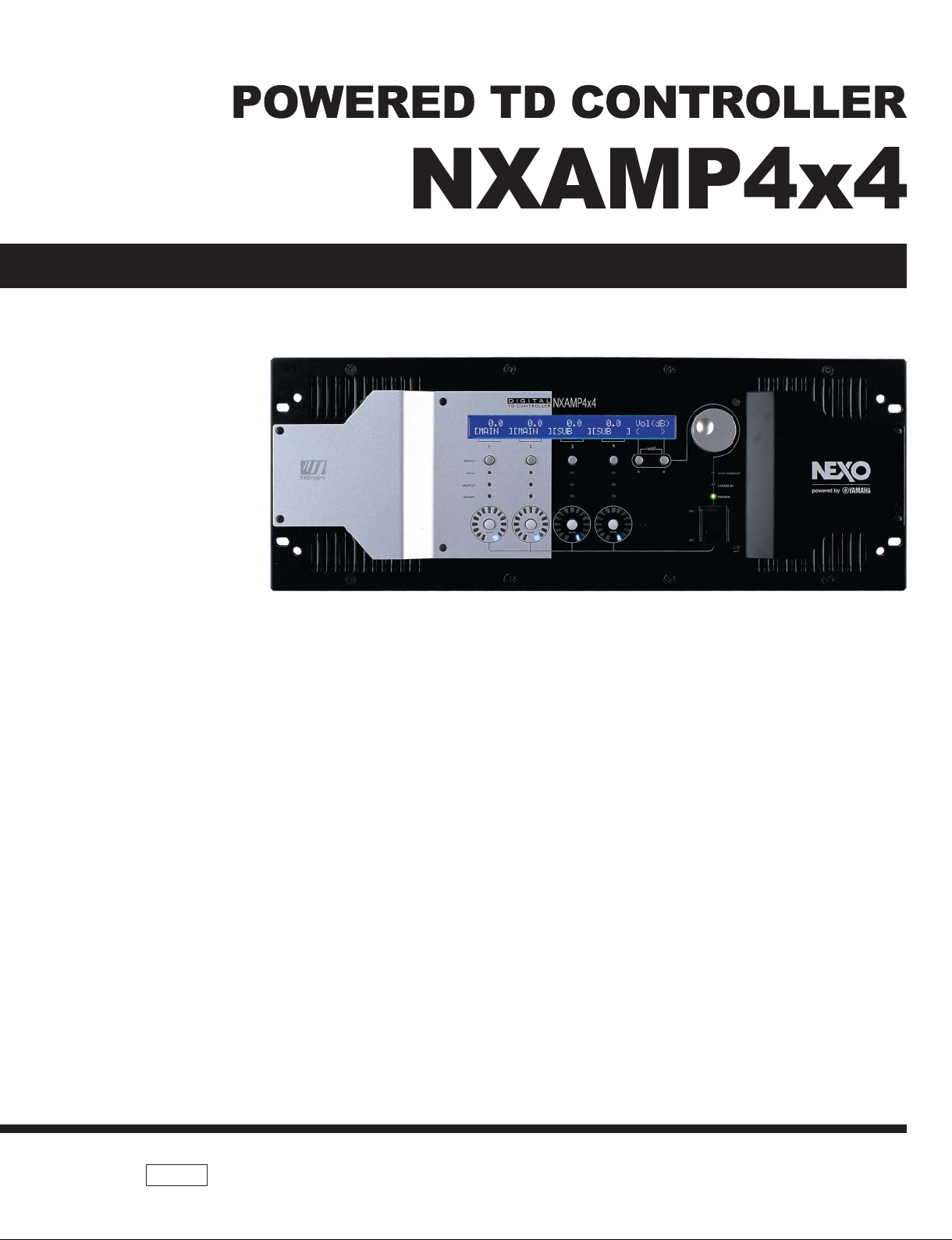
Page 1
SERVICE MANUAL
PA
011947
■ CONTENTS
PANEL LAYOUT
CIRCUIT BOARD LAYOUT
SERVICE PRECAUTIONS
OVERALL ASSEMBLY WIRING
DISASSEMBLY PROCEDURES
LSI PIN DESCRIPTION
IC BLOCK DIAGRAM
CIRCUIT BOARDS
TEST PROGRAM .......................................................................................64
テストプログラム
INSPECTIONS ...........................................................................................78
.............................................................................................................83
検査
UPDATING THE FIRMWARE .....................................................................88
ファームウェアのアップデート
PARTS LIST
BLOCK DIAGRAM
IC & DIODE FIGURES
CIRCUIT DIAGRAM
(目次)
(パネルレイアウト)
(ユニットレイアウト)
(サービス時の注意)
(LSI 端子機能表)
(IC ブロック図)
(シート基板図)
........................................................................................71
...........................................................3
........................................4
............................................5
(総組立配線図)
(分解手順)
.......................................................38
.............................................................44
....................................................................90
Copyright (c) NEXO S.A. All rights reserved. PDF ´09.10
.......................................... 7
...............................................25
...................................................37
Page 2
NXAMP4x4
WARNING: This product contains chemicals known to the State of California to cause cancer, or birth defects or other reproductive harm.
DO NOT PLACE SOLDER, ELECTRICAL/ELECTRONIC OR PLASTIC COMPONENTS IN YOUR MOUTH FOR ANY REASON WHAT SO
EVER!
Avoid prolonged, unprotected contact between solder and your skin! When soldering, do not inhale solder fumes or expose eyes to solder/flux
vapor!
If you come in contact with solder or components located inside the enclosure of this product, wash your hands before handling food.
IMPORTANT NOTICE FOR THE UNITED KINGDOM
Connecting the Plug and Cord
WARNING: THIS APPARATUS MUST BE EARTHED
IMPORTANT. The wires in this mains lead are coloured in accordance with the following code:
GREEN-AND-YELLOW: EARTH
BLUE: NEUTRAL
BROWN: LIVE
As the colours of the wires in the mains lead of this apparatus may not correspond with the coloured markings identifying the terminals in your
plug, proceed as follows:
The wire which is coloured GREEN and YELLOW must be connected to the terminal in the plug which is marked by the letter E or by the safety
earth symbol
The wire which is coloured BLUE must be connected to the terminal which is marked with the letter N or coloured BLACK.
The wire which is coloured BROWN must be connected to the terminal which is marked with the letter L or coloured RED.
or colored GREEN or colored GREEN and YELLOW.
WARNING
■
Components having special characteristics are marked and must be replaced with parts having specification equal to those originally
installed.
印の商品は、安全を維持するために重要な部品です。交換する場合は、安全のために必ず指定の部品をご使用ください。
(注意)
2
Page 3
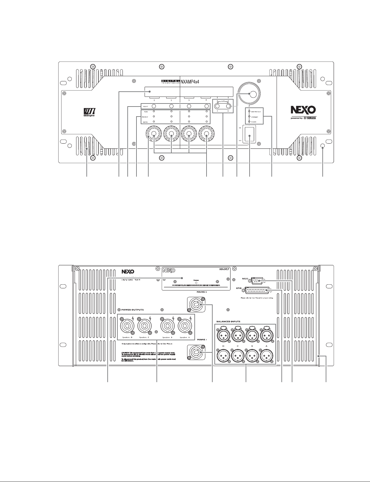
NXAMP4x4
PANEL LAYOUT
■
• Front Panel
Power switch
❶
Amplifier indicators
❷
LCD display
❸
Encoder
❹
Navigation buttons (A & B)
❺
Volume indicators
❻
(フロントパネル)
(パネルレイアウト)
Mute buttons
❼
Select buttons
❽
Channel indicators
❾
Air intakes
❿
Screw holes for handles
⓫
❶ 電源スイッチ
❷ アンプディスプレイ
❸ LCD ディスプレイ
❹ エンコーダー
❺
❶❷❼❸❿ ⓫❻❾❽❺❹
ナビゲーションボタン
(A&B)
❻ ボリュームディスプレイ
❼ ミュートボタン
❽ セレクトボタン
❾ チャンネルディスプレイ
❿ 吸気口
⓫ ハンドル用ネジ穴
• Rear Panel
Mains connectors
❶
Balanced audio inputs with link
❷
Expansion slot
❸
Power outputs
❹
RS-232 Firmware update port
❺
GPIO port
❻
Rear end mounting holes
❼
(リアパネル)
❸❹ ❻❷❶❺❼
❶ 電源端子
❷ バランスオーディオ入力(リンク付き)
❸ 拡張スロット
❹ パワー出力
❺ RS-232C ファームウェアアップデート用ポート
❻ GPIO ポート
❼ リアエンド取り付け穴
3
Page 4
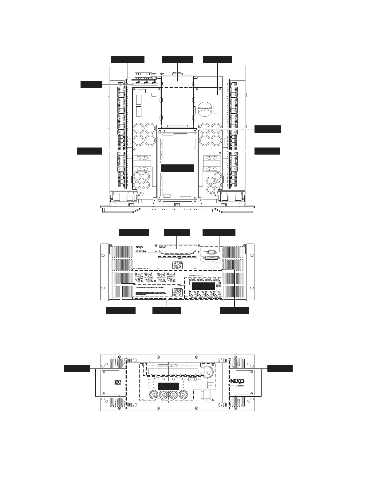
NXAMP4x4
CIRCUIT BOARD LAYOUT
■
RS232-GPI NX-DFLT
INANH
(PA unit)
(PA ユニット)
(ユニットレイアウト)
PSANHA
CONTROL
OPT-AN
PAANHPAANH
(PA unit)
(PA ユニット)
Rear Panel (リアパネル)
NX-DFLT
Front Panel (フロントパネル)
PAANH
(PA unit)
(PA ユニット)
PSANHBOUTANH
PN-AN
OPT-AN
RS232-GPI
INANH
PSANHA
PAANH
(PA unit)
(PA ユニット)
4
Page 5
NXAMP4x4
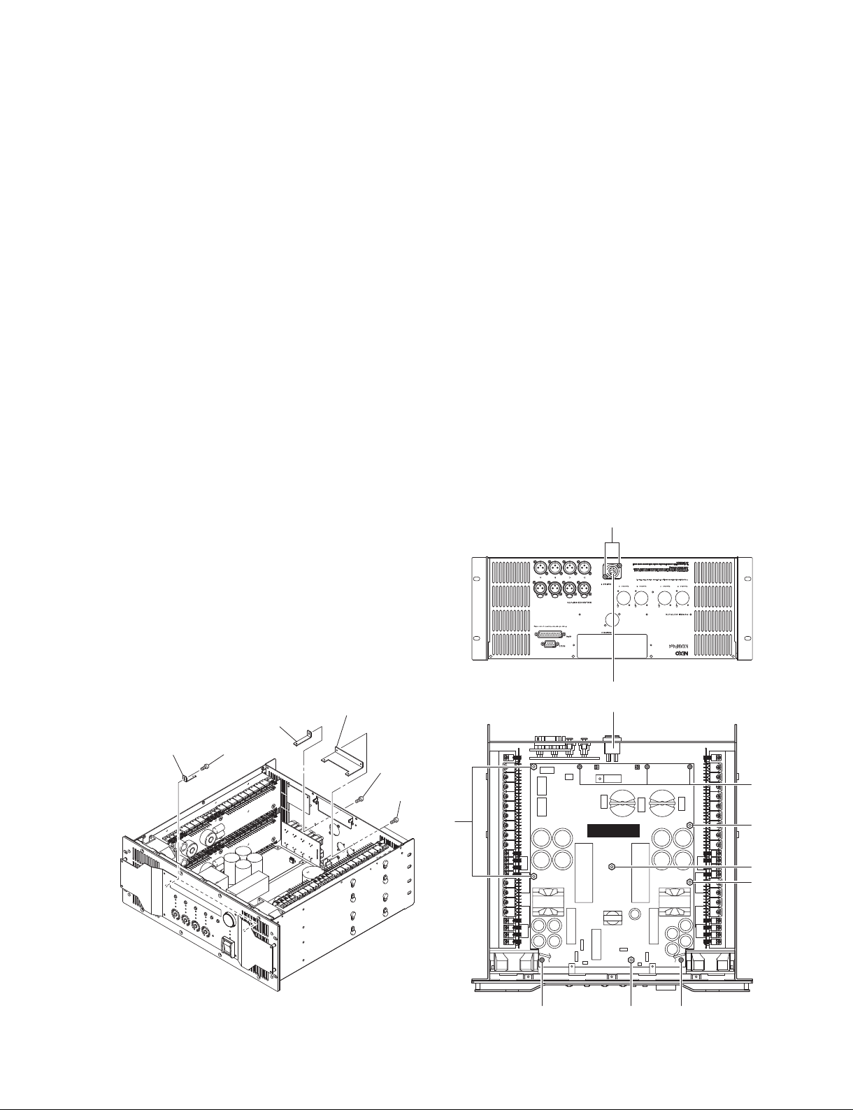
SERVICE PRECAUTIONS
■
(サービス時の注意)
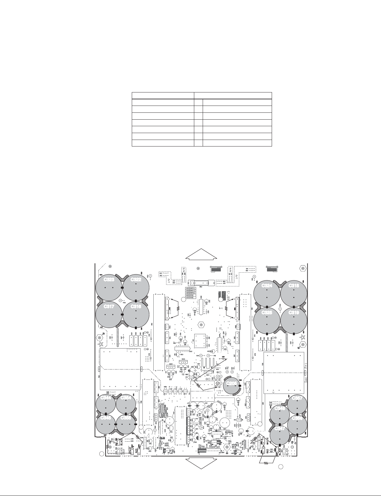
Safety measures
• Some component parts on the PSANH circuit board
maintain a high voltage even when the power is switched
off. For this reason to avoid an electrical shock, do not
touch the upper metallic part of the following capacitors
until the remaining voltage has discharged.
Capacitors /
C316, C317, C322, C323
C318, C319, C324, C325
C344, C354
C345, C355
C347, C356
C348, C357
C205
[Discharging Method]
Before starting the service work, connect discharging
resistors (220 Ω 10W) to the terminals indicated in the
figure below to discharge electricity. (7 points)
The required discharging time is about 10 seconds.
Check that the DC voltage between the terminals
measures close to 0 (zero) volts using a multi-meter to
make sure that the discharge is completed.
Note:
Do not touch the IC201 and its heat sink before
discharging the C205.
コンデンサ
安全対策
・ PSANH シートの部品の一部には電源 OFF 状態でも高
電圧が残ります。感電防止のため、残った電圧を放電
するまで下記のコンデンサの上部の金属部分に触らな
いでください。
Discharging point /
D305: + pin <=> D305: - pin
①
D306: + pin <=> D306: - pin
②
CN305 <=> CN316
③
CN307 <=> CN316
④
CN308 <=> CN309
⑤
CN310 <=> CN309
⑥
R213: lead <=> C201
⑦
[放電方法]
修理作業を始める前に、放電抵抗(220 Ω、10W)を
下図に示す放電用の端子間に接続します。(7 箇所)
放電に必要な時間は約 10 秒です。放電完了確認のため、
端子間電圧がほぼ 0(ゼロ)V であることをテスターで
チェックします。
注意:
C205 の放電完了まで IC201 とそれを固定しているヒー
トシンクには触らないでください。
放電箇所
PSANH circuit board
220 ohms/10W
C323 C322
C317 C316
C344 C354
C345 C355
CN316
4
CN307 CN305 CN308
3
220 ohms/10W
D305
1
220 ohms/
10W
220 ohms/10W
REAR
7
FRONT
220 ohms/
10W
C201
R213
D306
2
C205
220 ohms/10W
C324 C318
C325
6
CN310
220 ohms/10W
C319
C357
C348
C356
C347
CN309
5
5
Page 6
NXAMP4x4
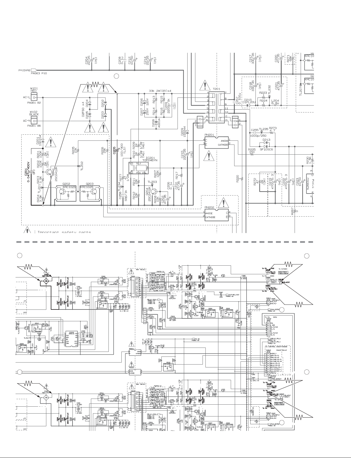
PSANH circuit diagram
1
2
C201
PSANHA only
220 ohms/10W
7
C205
PSANHA only
PSANHB only
PSANHA only
1
220 ohms/10W
D305
2
220 ohms/10W
D306
C316
C322
C317 C323
C318
C324
Primary
Secondary
220 ohms/10W
C305
ANH
C354C344
ANH
ANH
3
C316
ANH
C355C345
C356C347
C357C348
C307
ANH
To FAN
ANH
PSANHB
220 ohms/10W
ANH
ANH
ANH
ANH
ANH
ANH
To FAN
4
220 ohms/10W
PSANHA
5
6
XX
220 ohms/10W
C319 C325
6
Page 7
NXAMP4x4
OVERALL ASSEMBLY WIRING
■
This product has various cables (wires and connector
assemblies) inside. To prevent touching component to
the cables and/or connection mistake, perform the cable
connection and fixing cables according to the following
instructions referring the wiring diagram, P3 of the circuit
diagram.
Notice: Since the following pictures are taken of the
preproduction product, they may differ from the
commodity products in detail. However, the wiring
and so on is not so differ between them. So, refer
only to wiring and so on.
(総組立配線図)
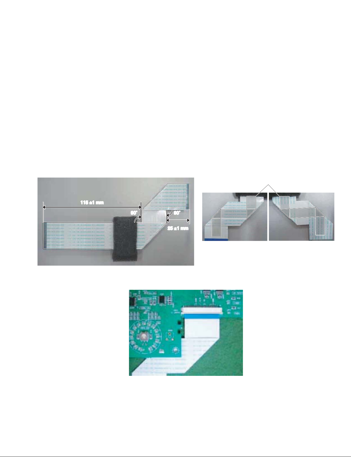
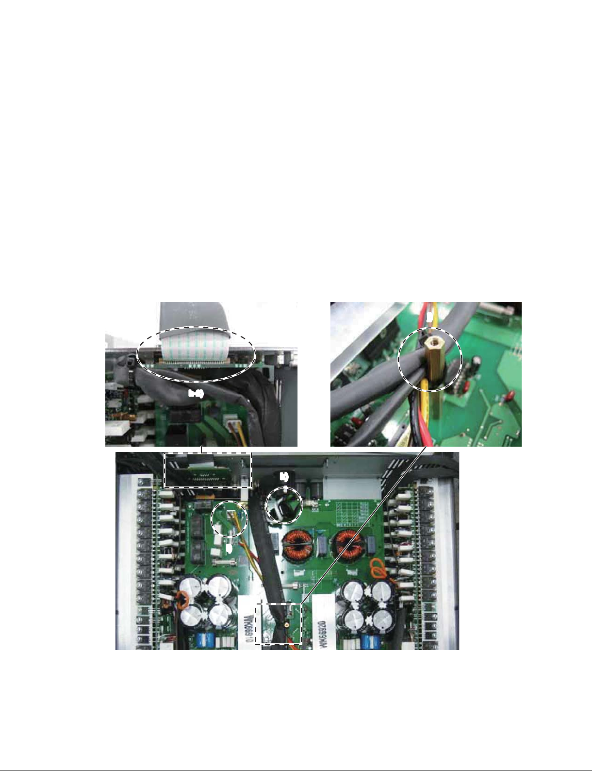
1. Wiring of the PN-AN circuit board
1) Process the PN FFC assembly (WR37010). (Fig. 1, 2)
2) Connect the PN FFC assembly (WR37010) to the PNAN circuit board. (Fig. 3)
3) Install the PN-AN circuit board to the front panel.
115 ±1 mm
本製品内部には色々な種類のケーブル(線材、束線)があり
ます。ケーブルの部品への接触やケーブルの接続ミスを防止
するために、回路図 3 ページのシート配線図を参照の上で下
記の指示にしたがってケーブルの接続と固定を行ってくださ
い。
注意: 掲載した写真は量産試作品を撮影したものですので
生産品とは細かい部分で異なりますが、配線周辺に
ついて違いはありません。配線作業用に限定して参
考にしてください。
1. PN-AN シートの配線
1) PNFFCAss'y(WR37010)を加工します。(図 1、2)
2) PNFFCAss'y(WR37010)を PN-AN シートへ接続し
ます。(図3)
3) PN-AN シートをフロントパネルへ取り付けます。
[635]
Fig. 1
(図 1)
90˚ 90˚
25 ±1 mm
Fix the bent part with adhesive tape [635].
(Attach it through the center of FFC.)
(折り曲げた部分をフィラメントテープ[635]で固定します。
(FFC の中心を通るように貼ります。))
Fig. 2
(図 2)
Fig. 3
* For details of wiring in the enclosure, refer to step “13.
Method of Fixing PN FFC Assembly”.
(図 3)
※ 筐体内部での配線についての詳細は「13. PNFFC
Ass'y の固定方法」を参照してください。
7
Page 8
NXAMP4x4
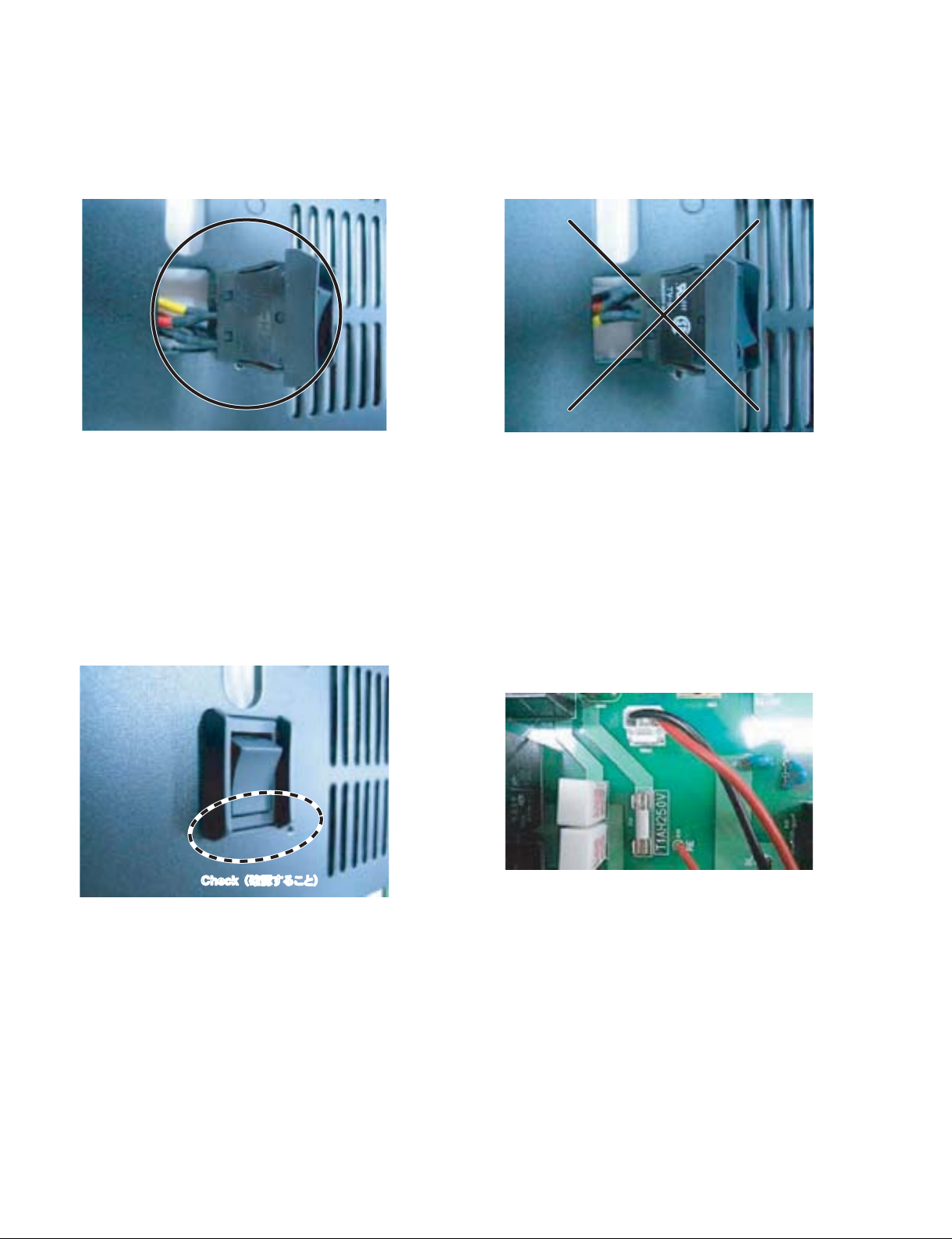
2. Wiring of the power switch
1) Install the power switch to the front panel with its
terminals set downward. (Fig. 4, 5)
Fig. 4
(図 4)
2) Confirm that the power switch is set to the off position as
shown in the figure. (Fig. 6)
3) Twist the wires of the power switch assembly more than
three times.
4) Connect the power switch connector assembly to the
connector (CN103) of the PSANHB circuit board. (Fig. 7)
2. 電源スイッチの配線
1) 端子の位置を下側にセットして、電源スイッチをフロ
ントパネルへ取り付けます。(図 4、5)
Fig. 5
(図 5)
2) 電源スイッチが図のように OFF ポジションにセットさ
れていることを確認します。(図 6)
3) 電源スイッチの線材を 3 回以上捻ります。
4) 電源スイッチの線材を PSANHB シートのコネクター
(CN103)へ接続します。(図 7)
Check (確認すること)
Fig. 6
(図 6)
Fig. 7
(図 7)
8
Page 9
NXAMP4x4
3. Wiring of the FAN
Connect the wire of the FAN to each connector. (Fig. 8)
4. Attaching of the support cushion
Attach the support cushion (WN15950) at the specified
area on the pattern side of the CONTROL circuit board.
(Fig. 9)
Note: Be sure to remove the oil and the dust, etc. on
the attaching surface before attaching the support
cushion.
Fig. 8
3. ファンの配線
ファンの線材を各コネクターへ接続します。(図8)
(図 8)
4. サポートクッションの取り付け
CONTROL シートパターン面の所定の位置にサポート
クッション(WN15950)を取り付けます。(図 9)
注意: サポートクッションを取り付ける前に、取り付
け面の油、埃などはきれいに取り除いてくださ
い。
Fig. 9
(図 9)
9
Page 10
NXAMP4x4
5. Wiring of the AC-INLET
a) Set a cord holder before installing the PSANHB circuit
board to the enclosure. (Fig. 10)
b) Set a ferrite-core at the specified area on the PSANHB
circuit board, and fasten the ferrite-core with a cord
holder. (Fig. 11)
Fig. 10
(図 10)
c) Pass the live and neutral wires of the AC-INLET through
the ferrite core’s hole twice and wind them to the ferrite
core.
Screw each screw terminal to the specified terminal.
(Fig. 12, 13)
Fasten the GND wire with a cord holder. (Fig. 12, 13)
Screwing torque: GND LINE 1.8N • m /
L, N LINE 0.78 • m
5. AC インレットの配線
a) PSANHB シートを取り付ける前に、インシュロックタ
イをセットします。(図 10)
b) PSANHB シートの所定の位置にフェライトコアをセッ
トし、インシュロックタイで固定します。(図 11)
Fig. 11
(図 11)
c) AC インレットの L、N の線をフェライトコアの穴に 2
回通して、フェライトコアに巻きつけます。
各端子を図のように固定します。(図 12、13)
GND 線をインシュロックタイで図のように固定しま
す。(図 12、13)
ネジ締め付けトルク: GNDLINE1.8 N・m /
L、NLINE0.78・m
10
U/J destination
Cord holder
(イン シュロックタイ)
Fig. 12
(U / J 仕向)
(図 12)
CHN destination
Cord holder
(イン シュロックタイ)
Fig. 13
(CHN 仕向)
(図 13)
Page 11
NXAMP4x4
d, e) Fix the wires to the terminal with the screws, and refer to
the fig. 14 and fig. 15 for the direction of each terminal.
Screw the GND wire’s screw terminal of the upper ACINLET as shown in the figure, and don’t fasten it with a
cord holder. (Fig. 14, 15)
Fig. 14
(図 14)
d
、
e)端子をネジで固定します。このとき端子の向きは図に
従ってください。
上側の AC インレットの GND 線を図のようにネジで固
定します。ただし、このときインシュロックタイで固
定しないでください。(図 14、15)
Fig. 15
(図 15)
11
Page 12
NXAMP4x4
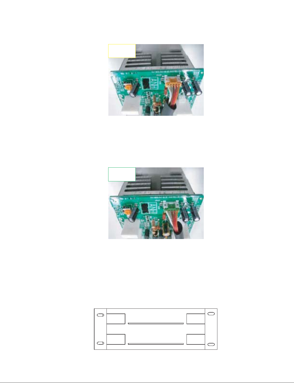
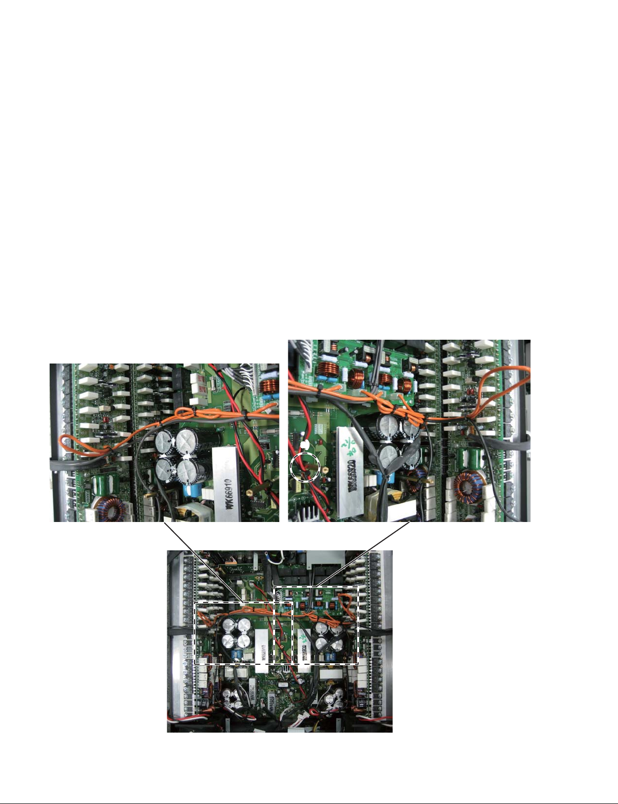
6. Wiring of the PA unit
Connect the wire to the CN401. (Fig. 18, 19, 20 and 21)
CN401
RED (赤)
NOTE: The wire to be connected is WK02080.
Install this PA unit on the upper left side of
enclosure.
Hereafter, this unit is called PA unit of CH1.
Fig. 18
6. PA ユニットの配線
下図のように CN401 へ線材を接続します。(図 18、
19、20、21)
(図 18)
注意: 線材(WK02080)を接続します。
この PA ユニットを筐体の上左側へ取り付け
ます。
これ以後、このユニットを CH1 の PA ユニッ
トと呼びます。
CN401
BLUE (青)
NOTE: The wire to be connected is WK17090.
Install this PA unit on the upper right side of
enclosure.
Hereafter, this unit is called PA unit of CH2.
Fig. 19
(図 19)
注意: 線材(WK17090)を接続します。
この PA ユニットを筐体の上右側へ取り付け
ます。
これ以後、このユニットを CH2 の PA ユニッ
トと呼びます。
12
Page 13
CN401
YELLOW (黄)
Fig. 20
NXAMP4x4
(図 20)
NOTE: The wire to be connected is WK17100.
Install this PA unit on the lower left side of
enclosure.
Hereafter, this unit is called PA unit of CH3.
CN401
GREEN (緑)
NOTE: The wire to be connected is WK17110.
Install this PA unit on the lower right side of
enclosure.
Hereafter, this unit is called PA-UNIT of CH4.
Fig. 21
注意: 線材(WK17100)を接続します。
この PA ユニットを筐体の下左側へ取り付け
ます。
これ以後、このユニットを CH3 の PA ユニッ
トと呼びます。
(図 21)
注意: 線材(WK17110)を接続します。
この PA ユニットを筐体の下右側へ取り付け
ます。
これ以後、このユニットを CH4 の PA ユニッ
トと呼びます。
* The following figure describes a layout drawing of
the PA units seen from the front panel. (Fig. 22)
CH1
RED
(赤)
CH3
YELLOW
(黄)
Fig. 22
PSANHA
PSANHB
(図 22)
※ 次の図は、フロントパネル側から見た PA ユニッ
トのレイアウト図です。(図 22)
CH2
BLUE
(青)
CH4
GREEN
(緑)
13
Page 14
NXAMP4x4
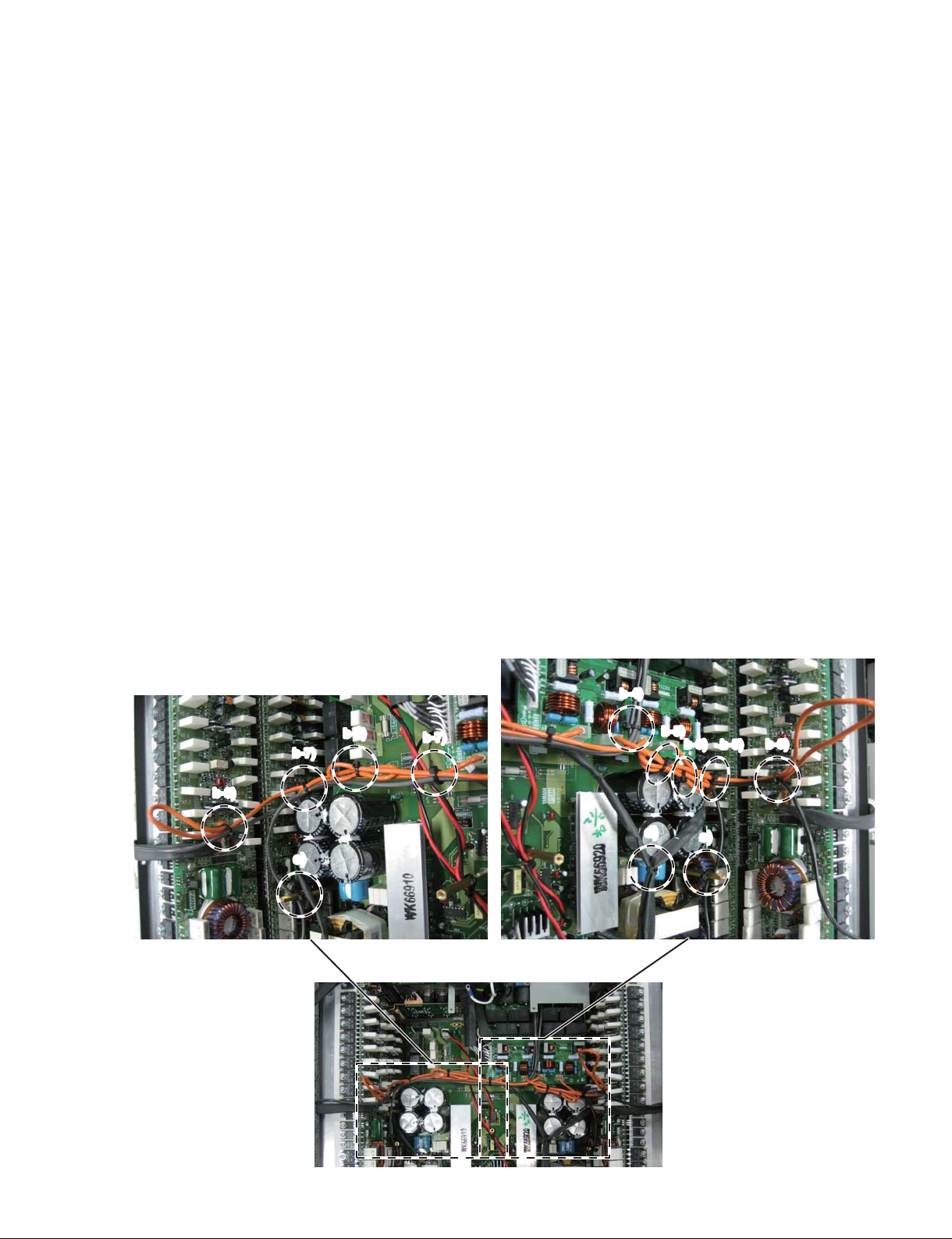
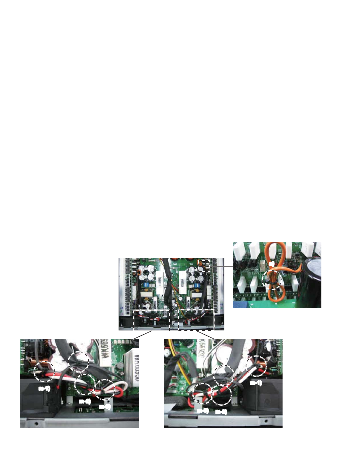
7. Wiring and fastening
Connect the following wires at first.
CN313: WK68740
CN203: WK66350
a) Fasten these wires (WK17900, WK17910 and WK94690)
with a cord holder to the hexagonal spacer. (Fig. 23)
Note: Do not fasten the wires (brown and yellow) of
WK94690 because they must be connected to
the PSANHA (upper PSANHA) circuit board
later.
b) Connect the wire (WN52520) of each PA unit (CH1–CH4)
to CH1–CH4 connectors of the OUTANH circuit board
referring the component location printed on the board.
(Fig. 23)
Way of fastening wire
b-1) Fold the wires of the lower PA unit at the center of
them.
b-2) Pull the wires of the upper PA unit toward the PA
unit. (Do not fold these wires.)
7. 配線と固定
初めに下記の線材を接続します。
CN313:WK68740
CN203:WK66350
a) 線材(WK17900、WK17910、WK94690)をインシュ
ロックタイで六角スペーサーへ固定します。(図 23)
注意: 束線(WK94690)の線材(茶色、黄色)は、
後で上側にある PSANHA シートへ接続するの
で、ここでは固定しません。
b) 各 PA ユ ニ ッ ト(CH1 〜 CH4)の線材(WN52520)
を、OUTANH シートに印刷された表示にしたがって
OUTANH シートのファストン端子へ接続します。
(図 23)
線材の固定方法
b-1)下側の PA ユニットの線材を図のように中央で折
りたたみます。
b-2)上側の PA ユニットの線材を PA ユニット側に引っ
張ります。
(この線材は折りたたまないでください。)
a)
14
Fig. 23
(図 23)
Page 15
NXAMP4x4
b-3) Then
fasten these wires with a cord holder as
shown in the figure.
b-4) Fasten these wires (WM04880 x 2, WK16820 x 2)
with a cord holder.
b-5) Fasten these wires (WN52520 x 2, WK16820 x 2)
with a cord holder (2 places).
b-6) Fasten these wires (WN52520, WK16820) with a
cord holder (1 place).
* Bend wire (WN52520) once.
b-7) Fasten these wires (WN52520 x 2, WM04880 x 2)
with a cord holder (2 places).
b-8) Fasten these wires (WN52520, WM04880) by wire
harness Tie (1 place).
* Bend wire (WN52520) once.
c) Connect the wire (WM04880) to connector (CN306) of
the PSANHA circuit board. Connect the wire (WK16820)
to the connector (CN317) of the PSANHB circuit board.
Fasten these wires (WM04880, WK16820) with a cord
holder to the hexagonal spacer as shown in the figure.
(Pass the wires to the PA unit side of a hexagonal
spacer)
d) Connect the wire (WK14210) of the PA unit (CH4) to the
connector (CN315) of the PSANHB circuit board. (Draw
the Black tube to the PA unit side.)
Pull the wire (WK14210) from PA unit to the direction of
T301 and fasten these wires (WK14200, WK14210) with
a cord holder. Before fastening, pull the wire (WK14200)
toward the front panel side in advance.
b-3)その後、これらの線材を図のようにインシュロッ
クタイで固定します。
b-4)線材(WM04880x2、WK16820x2)をインシュ
ロックタイで固定します。
b-5)線材(WN52520x2、WK16820x2)をインシュ
ロックタイで固定します。(2 箇所)
b-6)線材(WN52520、WK16820)をインシュロック
タイで固定します。(1 箇所)
※ WN52520 は一度折り返します。
b-7)線材(WN52520x2、WM04880x2)をインシュ
ロックタイで固定します。(2 箇所)
b-8)線材(WN52520、WM04880)をインシュロック
タイで固定します。(1 箇所)
※ WN52520 は一度折り返します。
c) 線材(WM04880)を PSANHA シートのコネクター
(CN306)へ、線材(WK16820)を PSANHB シート
のコネクター(CN317)へ接続します。
線材(WM04880、WK16820)を図のようにインシュロッ
クタイで六角スペーサーへ固定します。
(線材を六角スペーサーの PA ユニット側を通します)
d) PA ユニット(CH4)の線材(WK14210)を PSANHB シー
トの CN315 へ接続します。(スミチューブを PA ユニッ
ト側に寄せます。)
線材(WK14210)を PA ユニットから T301 の方向に
引っ張り、線材(WK14200、WK14210)をインシュロッ
クタイで固定します。このとき線材(WK14200)をフ
ロント側へ引っ張っておきます。
b-8)
b-7)
c)
b-3)
b-7)
b-4)
d)
b-5)
b-3)
c)
b-5)
b-6)
Fig. 24
(図 24)
15
Page 16
NXAMP4x4
e) Connect the wire (WK14210) of the PA unit (CH3) to the
connector (CN312) of the PSANHB circuit board. (Draw
the black tube to the PA unit side.)
Fasten the wire (WK14210) and the wire of the FAN with
a cord holder. (Fig. 22)
f) Twist the wires (white, red, black) of the PA unit more
than two times, and connect them to the terminals
according to the wire color displayed on the PSAN circuit
board. Fasten these wires (white, red, black) and wire
(WM04880) with a cord holder. (2 places)
Then bend the wires (white, red, black), and fasten them
with a cord holder. (Fig. 22)
g) Connect the wires (white, red, black) of PA unit to the
terminals in the same manner as step f).
Fasten these wires (white, red, black) and wire
(WK16820) with a cord holder (2 places). And then,
bend these wires (white, red, black) and fasten them
with a cord holder.
Fasten the wires (WK14210, WK14200) and the wire of
FAN with a cord holder.
h)
h-1) Fasten the wires (WK68740, WK14200, WK66350)
with a cord holder.
e) PA ユニット(CH3)の線材(WK14210)を PSANHB シー
トの CN312 へ接続します。(スミチューブを PA ユニッ
ト側に寄せます。)
線材(WK14210)と FAN の線材を図のようにインシュ
ロックタイで固定します。
f) PA ユニットの線材(白、赤、黒)を 2 回以上捻った後、
PSAN シートに表示された線材の色にしたがって各線
材をファストン端子へ接続します。そのとき、それら
の線材(白、赤、黒)と線材(WM04880)をインシュ
ロックタイで固定します。(2 箇所)
またそれら(白、赤、黒)の線材を折り曲げた後インシュ
ロックタイで固定します。
g) f)と同じ方法で、PA ユニットの線材(白、赤、黒)を
端子へ接続します。
それら(白、赤、黒)の線材を、線材(WK16820)と
一緒にインシュロックタイで固定します。(2 箇所)
またそれら(白、赤、黒)の線材を折り曲げた後、インシュ
ロックタイで固定します。
線材(WK14210、WK14200)と FAN の線材をまとめ
てインシュロックタイで固定します。
h)
h-1)線材(WK68740、WK14200、WK66350)をイン
シュロックタイで固定します。
16
e)
g)
g)
f)
f)
f)
h-1)
Fig. 25
(図 25)
g)
g)
Page 17
NXAMP4x4
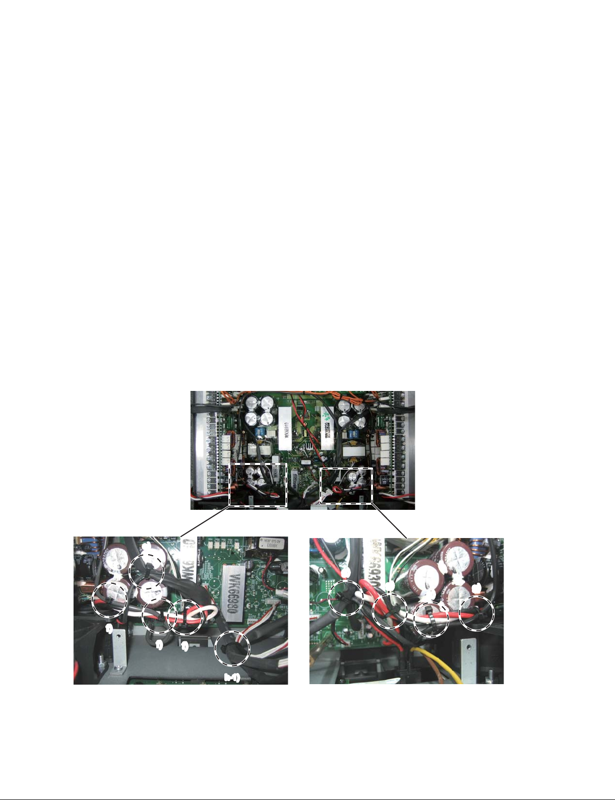
At the stage as shown in Fig. 26, connect the
following wires.
CN313: WK68760
CN201: WK68770
CN202: WK14200 from OUTANH board
CN203: WK66350 from PSANHB board
h-2) After connecting the wire (WM15830) to it, install
the RS232-GPI circuit board to the enclosure.
i) Twist the wires (yellow, brown) of the power switch
assembly more than three times, and connect it to the
connector (CN103) of the PSANHA circuit board.
j) Fasten these wires (WK17900, WK17910, WK94690 and
WK02090) with a cord holder to the hexagonal spacer.
k) Connect the wire of the AC-INLET according to the step
“5. Wiring of the AC-INLET”.
Note: Do not fasten the GND wire with a cord holder.
図 26 の段階で下記の線材を接続しておきます。
CN313:WK68760
CN201:WK68770
CN202:WK14200OUTANHシートから
CN203:WK66350PSANHBシートから
h-2)RS232-GPI シートに線材(WM15830)を接続し
た後、RS232-GPI シートを筐体へ取り付けます。
i) 電源 SW の線材(黄色、茶色)を 3 回以上捻った後、
PSANHA シートのコネクター(CN103)へ接続します。
j) 線材(WK17900、WK17910、WK94690、WK02090)
をインシュロックタイで六角スペーサーへ固定します。
k) 「5. AC インレットの配線」にしたがって AC インレッ
トの線材を接続します。
注意: GND 線材はインシュロックタイで固定しない
でください。
j)
h-2)
k)
i)
Fig. 26
(図 26)
17
Page 18
NXAMP4x4
l) Connect the wire (WK14210) of PA unit (CH1) to the
connect
(Draw a black tube to the PA unit side.)
Connect the wire (WK14210) of PA unit (CH2) to the
connector (CN315) of the PSANHA circuit board.
(Draw a black tube to the PA unit side.)
Fasten the wire (WK14210) and the wire of FAN with a
cord holder as shown in the figure. (Fig. 24)
m) Twist the wires (white, red, black) of the PA unit more
than two times, and connect them to the FASTON
terminals according to the wire color displayed on the
PSANHA circuit board.
m-1, 2) Fasten these wires (white, red, black) together
m-3) Bend these wires (white, red, black) and fasten
n) Fasten the wire (WN52520) with a cord holder.
(Fig. 25, 26)
Note: When connecting the connector assembly to
or (CN312) of the PSANHA circuit board.
with wires (WM04880, WK16820) with a cord
holder as shown in the figure.
them with a cord holder as shown in the figure.
the CONTROL circuit board、 confirm that the
connector housing pin number of the connector
assembly is the same as the connector pin
number of the circuit board.
l) PA ユニット(CH1)の線材(WK14210)を PSANHA シー
トのコネクター(CN312)へ接続します。(スミチュー
ブを PA-UNIT 側に寄せます。)
PA ユニット(CH2)の線材(WK14210)を PSANHA シー
トのコネクター(CN315)へ接続します。(スミチュー
ブを PA-UNIT 側に寄せます。)
線材(WK14210)と FAN の線材をインシュロックタ
イで図のように固定します。
m) PA ユニットの線材(白、赤、黒)を 2 回以上捻った
後、PSANHA シートに表示された線材の色にしたがっ
てファストン端子に接続します。
m-1、2)これらの線材(白、赤、黒)を線材(WM04880)、
(WK16820)と一緒にインシュロックタイで
固定します。
m-3) それら(白、赤、黒)の線材を折り曲げた後、
インシュロックタイで固定します。
n) 線材(WN52520)を図のようにインシュロックタイで
固定します。
注意: CONTROL シートに束線を接続するとき、
線材側のコネクターハウジングのピン数が
CONTROL シート側のコネクターのピン数と
同じであることを確認してください。
m-1)
l)
m-2)
m-3)
m-3)
n)
l)
m-1)
m-2)
18
Fig. 27
(図 27)
Page 19
NXAMP4x4
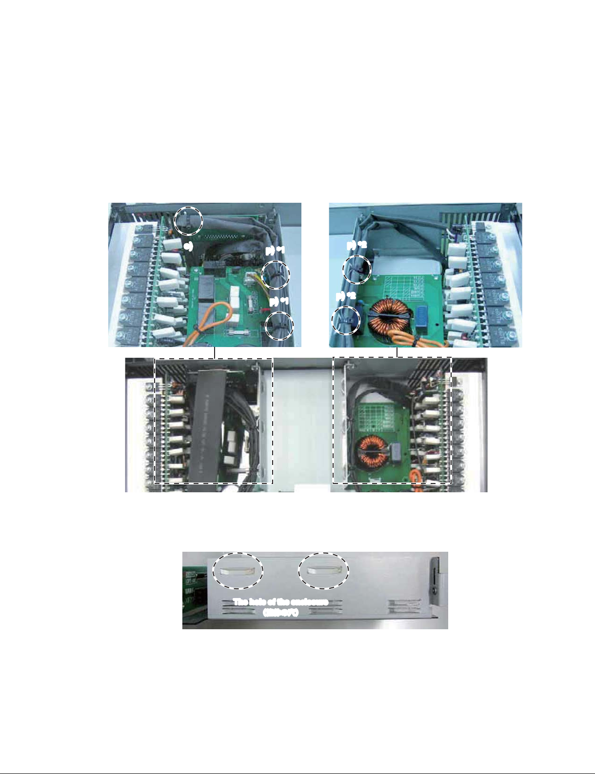
o) Fasten the wires (WK02080, WK17100) with a cord
holder to the hole of the RS232-GPI circuit board.
(Fig. 28)
p) 1) Fasten the wires (WK02080, WK17100 and
WK02070) with a cord holder to the hole of the
enclosure. (Fig. 28 *1, 29)
2) Fasten the wires (WK17090, WK17110) with a cord
holder to the hole of the enclosure. (Fig. 28 *2, 29)
o)
p)
p)
*1
*1
o) 線材(WK02080、WK17100)をインシュロックタイ
で RS232-GPI シートの穴へ固定します。(図 28)
p)1) 線材(WK02080、WK17100、WK02070)をイン
シュロックタイで筐体の穴へ固定します。
(図 28*1、29)
2) 線材(WK17090、WK17110)をインシュロック
タイで筐体の穴へ固定します。(図 28*2、29)
*2
p)
*2
p)
Fig. 28
(図 28)
The hole of the enclosure
(筐体の穴)
Fig. 29
(図 29)
19
Page 20
NXAMP4x4
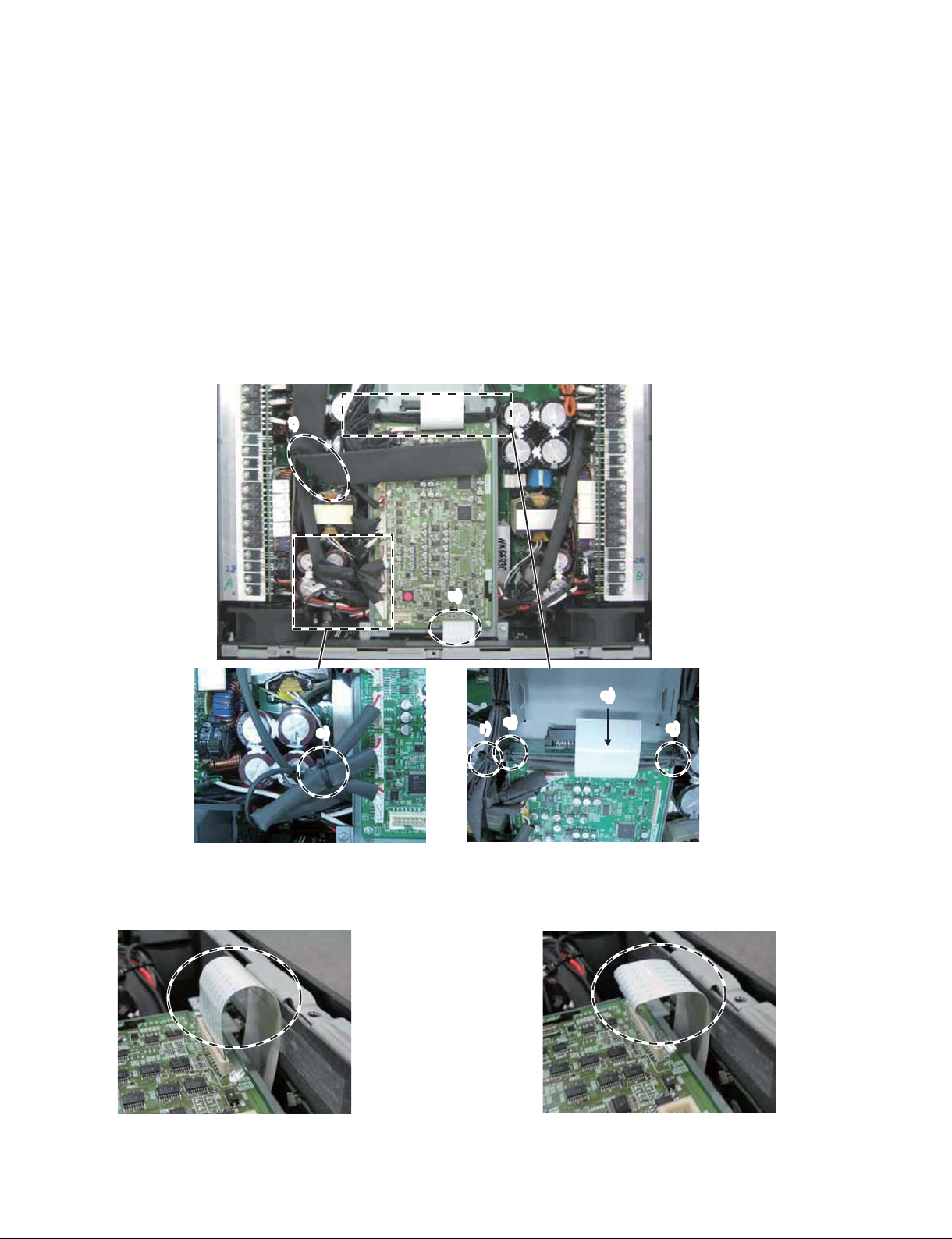
q) Fasten the wires (WK17090 and WK17110) with a cord
holder at the hole of the OPT-AN board. Then connect
the flat cable (WK02120). (Fig. 30)
r) Fasten the wires (WK02080, WK17090, WK17100,
WK17110 and WK02070) with a cord holder at the close
area to the OPT-AN circuit board. (Fig. 30)
s) Fasten the wires (WK68740, WK68760 and WK68770)
with a cord holder. (Fig. 30)
t) Bend the flat cable as shown in the figure. (Fig. 30)
u) Bend the flat cable to prevent it from touching the top
cover. (Fig. 31, 32)
t)
q) 線材(WK17090、WK17110)をインシュロックタイ
で OPT-AN シートの穴へ固定します。その後、フラッ
トケーブル(WK02120)を接続します。(図 30)
r) OPT-AN シートの横で線材(WK02080、WK17090、
WK17100、WK17110、WK02070)をインシュロック
タイで固定します。(図 30)
s) 線材(WK68740、WK68760、WK68770)を図のよう
にインシュロックタイで固定します。(図 30)
t) フラットケーブルを図のように折り曲げます。(図 30)
u) トップカバーとの接触を避けるためにフラットケーブ
ルを折り曲げます。(図 31、32)
u)
Fig. 31
(図 31)
s)
Fig. 30
r)
(図 30)
q)
q)
Fig. 32
q)
(図 32)
20
Page 21
NXAMP4x4
8. Color of the connectors connected to the connector CN012–CN015
Connect the connector assembly from the PA unit to the
CONTROL circuit board as shown in the figure below.
(Fig. 33)
CN012
RED
(赤)
CN013
BLUE
(青)
Fig. 33
8. CN012 − CN015 へ接続するコネクターの色
PAユニットからの束線を下図のようにCONTROLシー
トへ接続します。(図 33)
CN014
YELLOW
(黄)
(図 33)
CN015
GREEN
(緑)
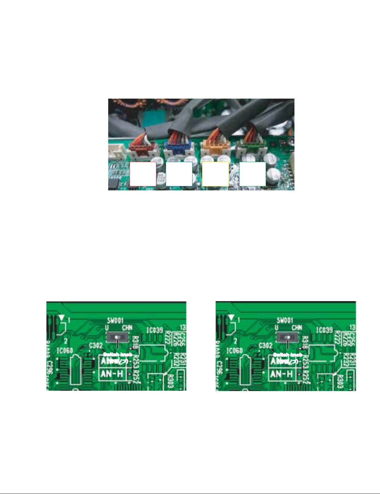
9. Change of the destination
Set the knob position of the switch SW001 on the
CONTROL circuit board as shown in the figure below.
(Fig. 34, 35)
U/J destination
Fig. 34
(U / J 仕向)
Switch knob
(切替ノブ)
(図 34)
9. 仕向け先の切り替え
CONTROL シートのスイッチ(SW001)を下図のよう
に切り替えます。(図 34、35)
CHN destination
Fig. 35
(CHN 仕向)
Switch knob
(切替ノブ)
(図 35)
21
Page 22
NXAMP4x4
10. Insulation distance between wire (WK17110) and primary side capacitor
Perform wiring of the connector assembly (WK17110)
with care so that its uncovered portion with the SUMI
tube does not touch the capacitor (C316) on primary
side of the PSANHA circuit board. (Fig. 36, 37)
Fig. 36
(図 36)
11. Adhesive cloth tape
Cover the two screws near R587 and R588 in each PA
unit [190, 220, 250 and 280] with adhesive cloth tape
[185, 215, 245 and 275] as shown in the figure below.
(Fig. 38)
10.束線 WK17110 と 1 次側ケミコンの絶縁距離
束線(WK17110)を配線するとき、スミチューブに覆
われていない部分が PSANHA シートの 1 次側にあるコ
ンデンサ(C316)に接触しないように注意してくださ
い。(図 36、37)
Fig. 37
(図 37)
11.アセテートクロス粘着テープ
各 PA ユ ニ ッ ト[190、220、250、280] の R587、
R588 の直近にある 2 つのネジを下図のようにアセテー
トクロステープ[185、215、245、275]で覆います。
(図 38)
22
Fig. 38
(図 38)
Page 23
NXAMP4x4
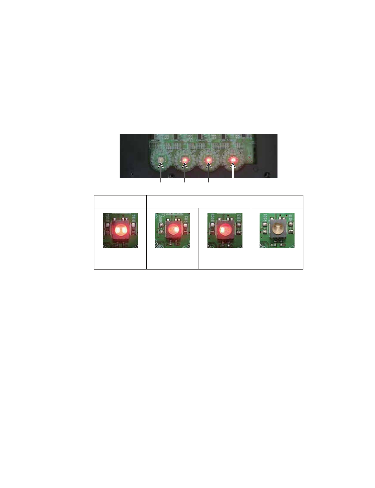
12. Confirmation of Switch LED lighting
With the front panel 2 uninstalled, confirm that the LEDs
of switches (SW003–SW006) light. (Fig. 39)
Procedure
1. Press the power switch of this unit to turn on the
power.
2. Press the switches (SW003–SW006) on the PN-AN
circuit board, and confirm that both LEDs of each
switch light.
SW003 SW004 SW005 SW006
OK NG
12.スイッチ LED 点灯確認
フロントパネル2を取り外した状態で、スイッチ
(SW003 〜 SW006)の LED が点灯することを確認し
ます。(図 39)
手順
1. 本機の電源スイッチを ON にします。
2. PN-AN シートのスイッチ(SW003 〜 SW006)
を押し、各スイッチの両方の LED が点灯すること
を確認します。
Lighting of both
(両方とも点灯)
Left is turned off
(左が消灯)
Fig. 39
Right is turned off
(右が消灯)
(図 39)
Turning off of both
(両方とも消灯)
23
Page 24
NXAMP4x4
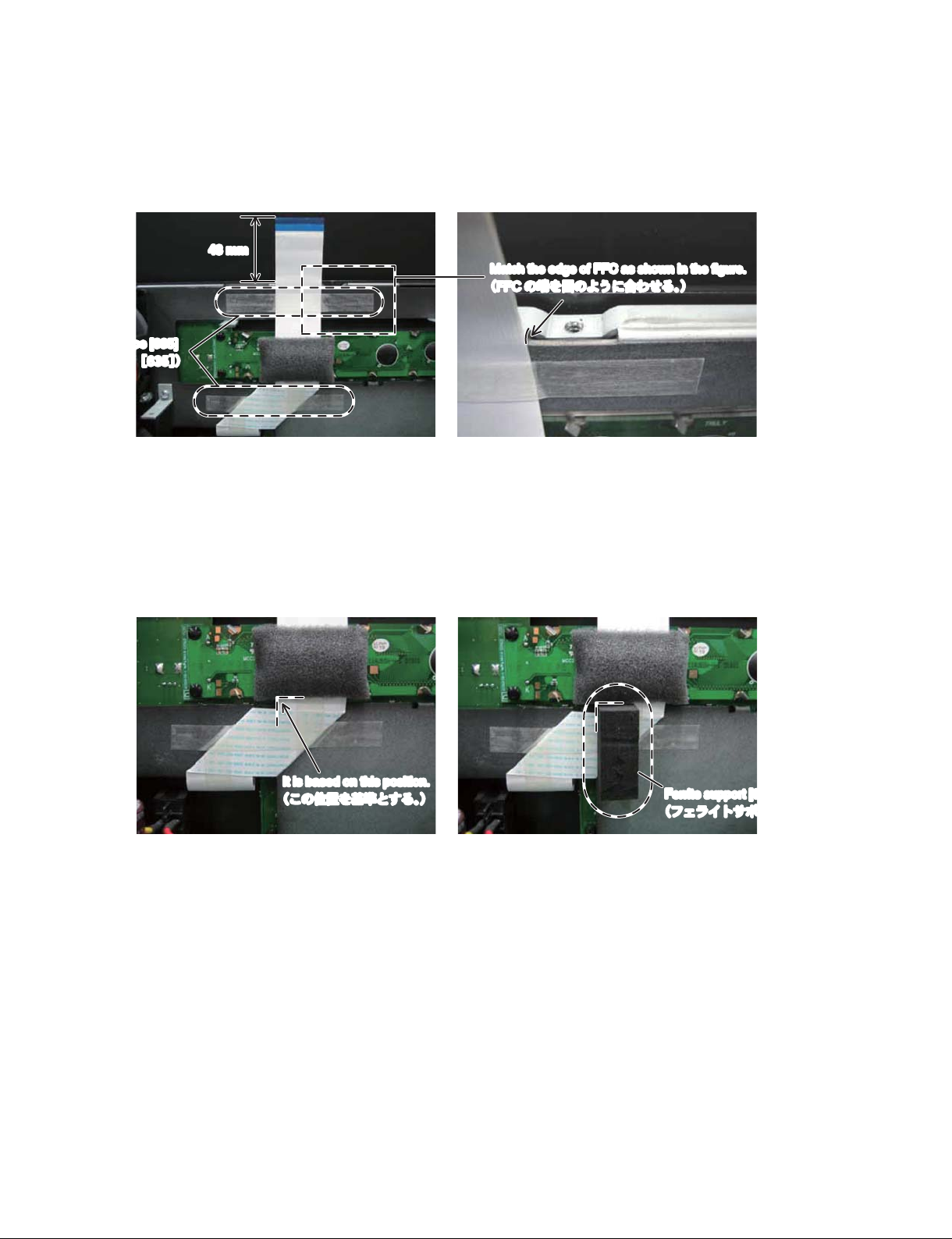
13. Method of Fixing PN FFC Assembly
Fix the PN FFC assembly with the adhesive tape [635]
as shown in the figure (2 places). (Fig. 40)
43 mm
Adhesive tape [635]
(粘着テープ[635])
Attach the ferrite support 1 [636] to the position as
shown in the figure below left. (Fig. 41)
(The figure below right shows the attached state.)
Fig. 40
13.PNFFCAss'y の固定方法
PNFFCAss'y を図のように粘着テープ[635]で固定
します(2 箇所)。(図 40)
Match the edge of FFC as shown in the figure.
(FFC の端を図のように合わせる。)
(図 40)
下左図に示す位置にフェライトサポート 1[636]を貼
り付けます。(図 41)
(下右図は貼り付けた状態を示します。)
24
It is based on this position.
(この位置を基準とする。)
Fig. 41
Ferrite support [636]
(フェライトサポート[636])
(図 41)
Page 25
NXAMP4x4
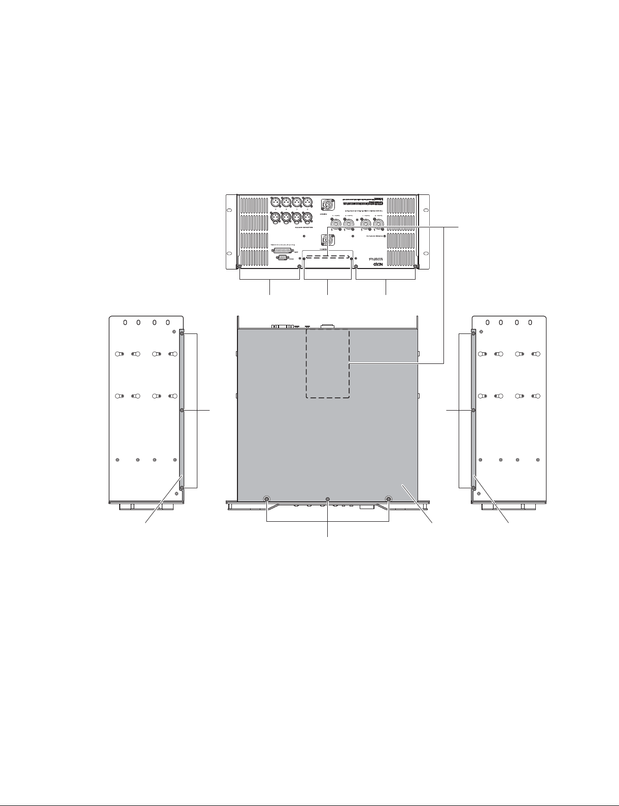
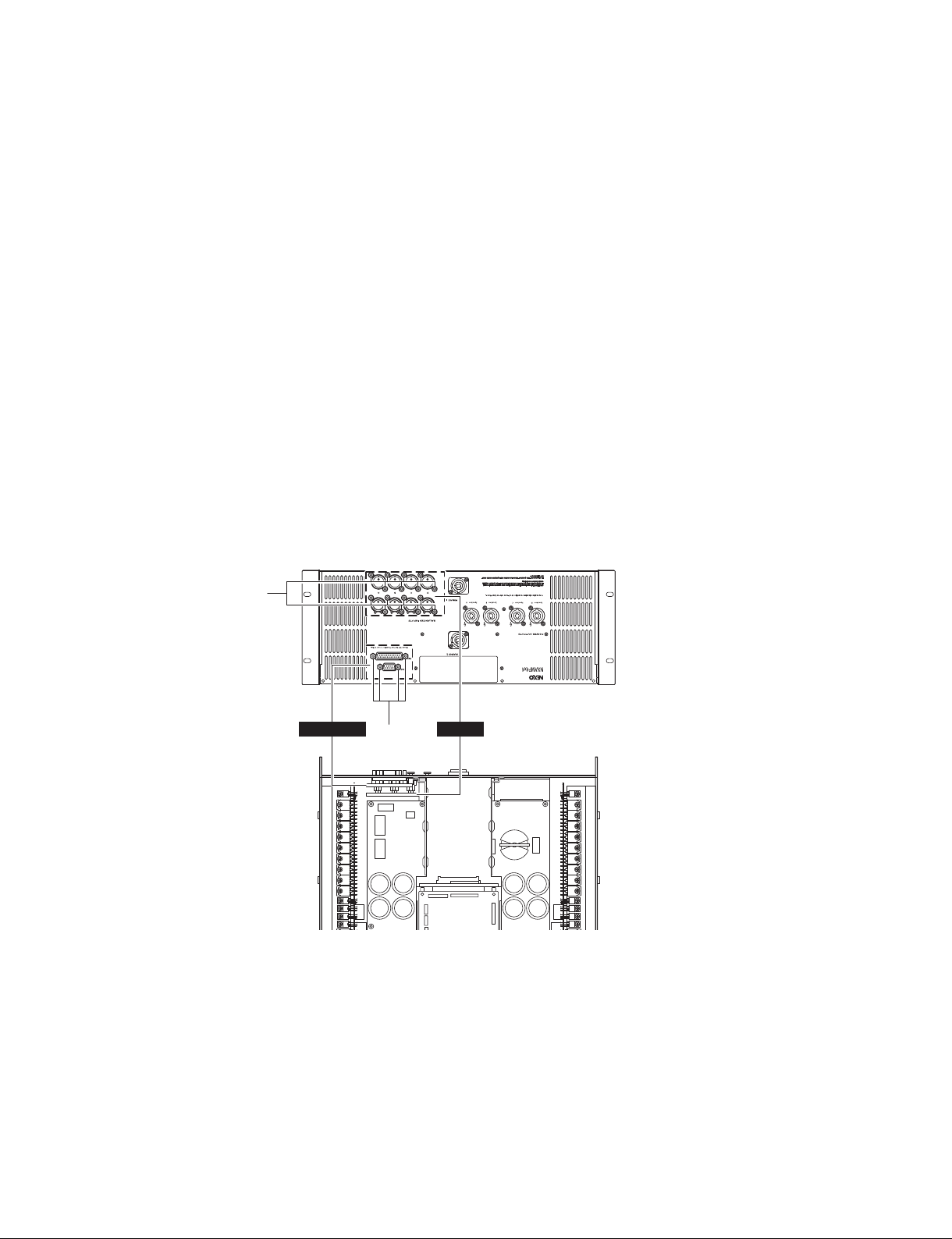
DISASSEMBLY PROCEDURES
■
(分解手順)
1. Top Cover and NX-DFLT Card (Time required: about 3 minutes)
1-1. Remove the thirteen (13) screws marked [800]. The
top cover can then be removed. (Fig.1)
1-2. Remove the two (2) screws marked [770]. The NX-
DFLT card can then be removed. (Fig. 1)
[800] [800][770]
1. トップカバー、NX-DFLT カード
(所要時間:約 3 分)
1-1. [800]のネジ 13 本を外し、トップカバーを外します。
(図 1)
1-2. [770]のネジ 2 本を外し、NX-DFLT カードを外しま
す。(図 1)
NX-DFLT card
(NX-DFLT カード)
Top cover
(トップカバ ー )
[800] [800]
[800]
[770]: BIND HEAD TAPPING SCREW-S 3x6 MFZN2B3 (--)
[800]: BIND HEAD TAPPING SCREW-B 4x8 MFZN2B3 (--)
Fig. 1
(図 1)
Top cover
(トップカバ ー )
S タイト+ BIND
B タイト+ BIND
Top cover
(トップカバ ー )
25
Page 26
NXAMP4x4
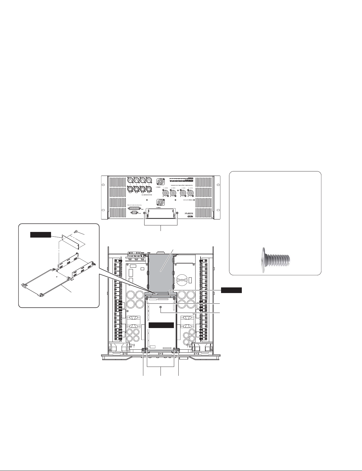
2. CONTROL Circuit Board, OPT angle and OPTAN Circuit Board
(Time required: about 10 minutes)
2-1. Remove the top cover and the NX-DFLT card.
(See procedure 1.)
2-2. Disconnect the connector assemblies from the
CONTROL circuit board. (Fig. 2)
2-3. Re move the fo ur (4) sc rews ma rked [580]. The
CONTROL circuit board can then be removed. (Fig. 2)
2-4. Remove the two (2) screws marked [550], one (1)
screw marked [555] and the two (2) screws marked
[560]. The OPT angle can then be removed together
with the OPT-AN circuit board. (Fig. 2)
2-5. Remove the two (2) screws marked [530]. The OPT-
AN circuit board and the OPT angle can then be
separated. (Fig. 2)
OPT-AN
[530]
[560]
2. CONTROL シート、OPT アングル、OPT-AN シー
ト(所要時間:約 10 分)
2-1. トップカバー、NX-DFLT カードを外します。
(1 項参照)
2-2. CONTROL シートから束線を外します。(図 2)
2-3. [580]のネジ 4 本を外し、CONTROL シートを外し
ます。(図 2)
2-4. [550]のネジ 2 本、[555]のネジ 1 本、[560]のネ
ジ 2 本を外し、OPT アングルを OPT-AN シートと共
に外します。(図 2)
2-5. [530]のネジ 2 本を外し、OPT-AN シートと OPT
アングルを別けます。(図 2)
CAUTION
The figure below shows the screw
marked [555] head shape.
To avoid the unit malfunction, make sure
the screw marked [555] head shape is
same as shown below before
assembling the OPT angle.
[555]のネジ頭形状を下図に示します。
動作不良防止のため、OPT アングルを取り
OPT angle
(OPT アングル)
付ける前に、[555]のネジ頭形状が下図のと
おりであることを確認してください。
26
OPT angle
(OPT アングル)
CONTROL
[580][550] [550]
[530]: BIND HEAD TAPPING SCREW-S 3x6 MFZN2W3 (--)
[550]: BIND HEAD TAPPING SCREW-S 3x6 MFZN2W3 (--)
[555]: BIND HEAD TAPPING SCREW-S 3x6 MFZN2B3 (--)
[560]: BIND HEAD TAPPING SCREW-S 3x6 MFZN2B3 (--)
[580]: BIND HEAD TAPPING SCREW-S 3x6 MFZN2W3 (--)
Fig. 2
(図 2)
OPT-AN
[580]
[555]
S タイト+ BIND
S タイト+ BIND
S タイト+ BIND
S タイト+ BIND
S タイト+ BIND
Page 27
NXAMP4x4
3. PSANHA Circuit Board (Time required: about 15 minutes)
3-1. Remove the top cover and the NX-DFLT card.
(See procedure 1.)
3-2. Remove the CONTROL circuit board and the OPT
angle. (See procedure 2.)
3-3. Remove the two (2) screws marked [150A], and remove
the upper ACPS connector assembly. (Fig. 3)
3-4. Disconnect the connector assemblies from the
PSANHA circuit board. (Fig. 3)
3-5. Remove the nine (9) screws marked [450] and the
one (1) hexagonal spacer marked [440]. The PSANHA
circuit board can then be removed. (Fig. 3)
Upper ACPS connector assembly
(上側の ACPS 束線)
3. PSANHA シート(所要時間:約 15 分)
3-1. トップカバー、NX-DFLT カードを外します。
(1 項参照)
3-2. CONTROL シート、OPT アングルを外します。
(2 項参照)
3-3. [150A]のネジ 2 本を外し、上側の ACPS 束線を外
します。(図 3)
3-4. PSANHA シートから束線を外します。(図 3)
3-5. [450]のネジ 9 本、[440]の六角スペーサー 1 個を
外し、PSANHA シートを外します。(図 3)
[150A]
[450]
PSANHA
[450]
[150A]: FLAT HEAD TAPPING SCREW-B 3x8 MFZN2B3 (--)
[440]: HEXAGONAL SPACER H=50 B=5.5 (--)
[450]: BIND HEAD TAPPING SCREW-S 3x6 MFZN2W3 (--)
Fig. 3
六角スペーサー
(図 3)
[450]
[440]
[450]
B タイト+ FLAT
S タイト+ BIND
27
Page 28
NXAMP4x4
4. OUTANH Circuit Board (Time required: about 20 minutes)
4-1. Remove the top cover and the NX-DFLT card.
(See procedure 1.)
4-2. Remove the CONTROL circuit board and the OPT
angle. (See procedure 2.)
4-3. Remove the PSANHA circuit board. (See procedure 3.)
4-4. Disconnect the connector assemblies from the
OUTANH circuit board. (Fig. 4)
4-5. Remove the eight (8) screws marked [320], the one
(1) screw marked [330] and the one (1) screw marked
[325]. The OUTANH circuit board can then be removed
together with the two (2) insulation sheets and the two
(2) shields. (Fig. 4)
4-6. Remove the three (3) plastic rivets marked [317]. The
OUTANH circuit board can be separated from the two
(2) insulation sheets and the two (2) shields attached
to them. (Fig. 4)
Note: The two (2) insulation sheets and the two (2)
shields can not be separated because they are
attached each other with both side adhesive
tapes.
4. OUTANH シート(所要時間:約 20 分)
4-1. トップカバー、NX-DFLT カードを外します。
(1 項参照)
4-2. CONTROL シート、OPT アングルを外します。
(2 項参照)
4-3. PSANHA シートを外します。(3 項参照)
4-4. OUTANH シートから束線を外します。(図 4)
4-5. [320]のネジ 8 本、[330]のネジ 1 本、[325]のネ
ジ 1 本を外し、OUTANH シートを絶縁シート 2 枚、
シールド 2 枚と共に外します。(図 4)
4-6. [317]のプラスチックリベット3個を外し、
OUTANH シートを絶縁シート 2 枚とこれらのシート
に貼付されたシールド 2 枚から別けます。(図 4)
注: 絶縁シート 2 枚とシールド 2 枚は、両面テー
プで互いに貼り付けられているために分離す
ることはできません。
[330]
[317]
OUTANH
Insulation sheet 2
(絶縁シート 2)
Shield 2
(シールド 2)
Shield 1
(シールド 1)
Insulation sheet 1
(絶縁シート 1)
[317]: PLASTIC RIVET NRP-345 (--)
[320]: FLAT HEAD TAPPING SCREW-B 3x8 MFZN2B3 (--)
[325]: BIND HEAD TAPPING SCREW-S 3x6 MFZN2W3 (--)
[330]: BIND HEAD TAPPING SCREW-B 3x8 MFZN2B3 (--)
[320]
OUTANH
プラスチックリベット
Fig. 4
(図 4)
[325]
B タイト+ FLAT
S タイト+ BIND
B タイト+ BIND
28
Page 29
NXAMP4x4
5. PSANHB Circuit Board (Time required: about 25 minutes)
5-1. Remove the top cover and the NX-DFLT card.
(See procedure 1.)
5-2. Remove the CONTROL circuit Board and the OPT
angle. (See procedure 2.)
5-3. Remove the PSANHA circuit Board. (See procedure 3.)
5-4. Remove the OUTANH circuit Board. (See procedure 4.)
5-5. Remove the two (2) screws marked [150B], and remove
the lower ACPS connector assembly. (Fig. 5)
5-6. Remove the two (2) screws marked [390], and remove
the PS Angle 1. (Fig. 5)
5-7. Remove the one (1) screw marked [396], and remove
the GND Angle. (Fig. 5)
5-8. Remove the two (2) screws marked [410], and remove
the two (2) pieces of PS Angle 2. (Fig. 5)
5-9. Disconnect the connector assemblies from the
PSANHB circuit board. (Fig. 5)
5-10. Remove the five (5) screws marked [100], the five
(5) hexagonal spacers marked [90] and the one (1)
hexagonal spacer marked [95]. The PSANHB circuit
board can then be removed. (Fig. 5)
[90]: HEXAGONAL SPACER H=81.4 B=5.5 (--)
[95]: HEXAGONAL SPACER H=41 B=5.5 (--)
[100]: BIND HEAD TAPPING SCREW-S 3x6 MFZN2W3 (--)
S タイト+ BIND
[150]: FLAT HEAD TAPPING SCREW-B 3x8 MFZN2B3 (--)
B タイト+ FLAT
[390]: BIND HEAD TAPPING SCREW-S 3x6 MFZN2B3 (--)
S タイト+ BIND
[396]: BIND HEAD TAPPING SCREW-S 3x6 MFZN2B3 (--)
S タイト+ BIND
[410]: BIND HEAD TAPPING SCREW-S 3x6 MFZN2W3 (--)
S タイト+ BIND
GND angle
PS angle 2
(PS アングル 2)
(GND アングル)
[410]
六角スペーサー
六角スペーサー
PS angle 1
(PS アングル 1)
[396]
[390]
5. PSANHB シート(所要時間:約 25 分)
5-1. トップカバー、NX-DFLT カードを外します。
(1 項参照)
5-2. CONTROL シート、OPT アングルを外します。
(2 項参照)
5-3. PSANHA シートを外します。(3 項参照)
5-4. OUTANH シートを外します。(4 項参照)
5-5. [150B]のネジ 2 本を外し、下側の ACPS 束線を外
します。(図 5)
5-6. [390]のネジ 2 本を外し、PS アングル 1 を外します。
(図 5)
5-7. [396]のネジ 1 本を外し、GND アングルを外します。
(図 5)
5-8. [410]のネジ 2 本を外し、2 つの PS アングル 2 を
外します。(図 5)
5-9. PSANHB シートから束線を外します。(図 5)
5-10.[100]のネジ 5 本、[90]の六角スペーサー 5 個、[95]
の六角スペーサー 1 個を外し、PSANHB シートを外
します。(図 5)
[150B]
Lower ACPS connector assembly
(下側の ACPS 束線)
[100]
[90]
Fig. 5
(図 5)
PSANHB
[90] [100][100]
[90]
[95]
[90]
29
Page 30
NXAMP4x4
6. INANH Circuit Board (Time required: about 7minutes)
6-1. Remove the top cover and the NX-DFLT card.
(See procedure 1.)
6-2. Disconnect the connector assembly from the INANH
circuit board. (Fig. 6)
6-3. Remove the sixteen (16) screws marked [70]. The
INANH circuit board can then be removed. (Fig. 6)
7. RS232-GPI Circuit Board (Time required: about 7 minutes)
7-1. Remove the top cover and the NX-DFLT card.
(See procedure 1.)
7-2. Disconnect the flat cable from the RS232-GPI circuit
board. (Fig. 6)
7-3. Remove the four (4) hexagonal lock screws marked
[370]. The RS232-GPI circuit board can then be
removed. (Fig. 6)
6. INANH シート(所要時間:約 7 分)
6-1. トップカバー、NX-DFLT カードを外します。
(1 項参照)
6-2. INANH シートから束線を外します。(図 6)
6-3. [70]のネジ 16 本を外し、INANH シートを外します。
(図 6)
7. RS232-GPI シート(所要時間:約 7 分)
7-1. トップカバー、NX-DFLT カードを外します。
(1 項参照)
7-2. RS232-GPI シートからフラットケーブルを外します。
(図 6)
7-3. [370]の六角ロックネジ 4 本を外し、RS232-GPI シー
トを外します。(図 6)
[70]
RS232-GPI
[70]: BIND HEAD TAPPING SCREW-B 2.6x8 MFZN2B3 (--)
[370]: HEXAGONAL LOCK SCREW (--)
[370]
INANH
6 角ロックネジ
B タイト+ BIND
30
Fig. 6
(図 6)
Page 31

NXAMP4x4
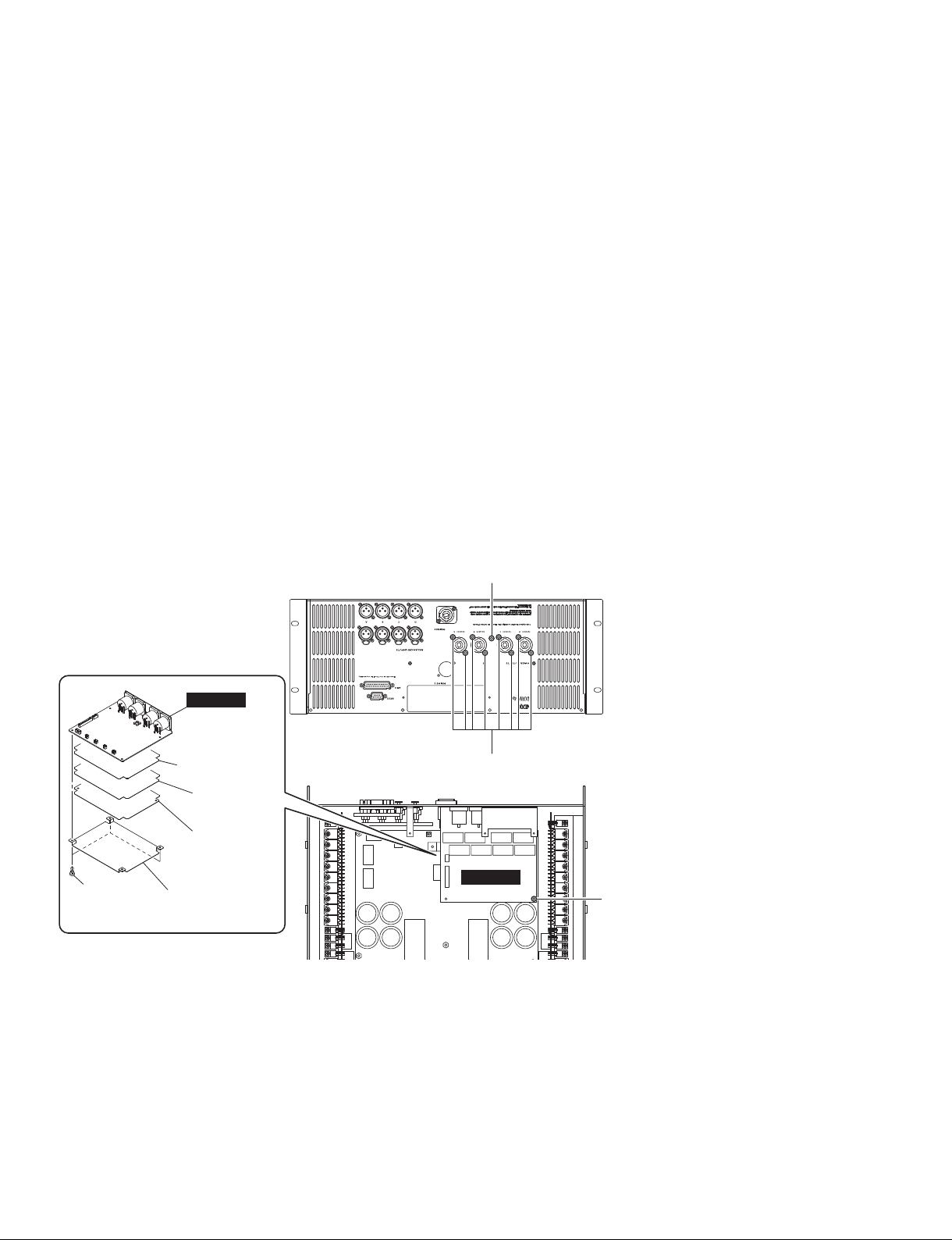
8. Upper left (CH1) PA unit (Time required: about 15 minutes)
8-1. Remove the top cover and the NX-DFLT card.
(See procedure 1.)
8-2. Remove the CONTROL circuit board and the OPT
angle. (See procedure 2.)
8-3. Disconnect the connector assemblies which connects
the upper left PA unit and other units. (Fig. 7)
8-4. Remove the four (4) screws mar ked [820A], and
remove the four (4) screw covers marked [810A].
(Fig. 7)
8-5. Remove the six (6) screws marked [270]. The upper
left PA unit can then be removed. (Fig. 7)
9. Upper right (CH2) PA unit (Time required: about 15 minutes)
9-1. Remove the top cover and the NX-DFLT card.
(See procedure 1.)
9-2. Remove the CONTROL circuit board and the OPT
angle. (See procedure 2.)
9-3. Disconnect the connector assemblies which connects
the upper right PA unit and other units. (Fig. 7)
9-4. Remove the four (4) screws mar ked [820B], and
remove the four (4) screw covers marked [810B].
(Fig. 7)
9-5. Remove the six (6) screws marked [300]. The upper
right PA unit can then be removed. (Fig. 7)
8. 上左側(CH1)PA ユニット(所要時間:約 15 分)
8-1. トップカバー、NX-DFLT カードを外します。
(1 項参照)
8-2. CONTROL シート、OPT アングルを外します。
(2 項参照)
8-3. 上左側の PA ユニットと他のユニットを接続している
束線を外します。(図 7)
8-4. [820A]のネジ 4 本を外し、[810A]のネジカバー 4
個を外します。(図 7)
8-5. [270]のネジ 6 本を外し、上左側の PA ユニットを
外します。(図 7)
9. 上右側(CH2)PA ユニット(所要時間:約 15 分)
9-1. トップカバー、NX-DFLT カードを外します。
(1 項参照)
9-2. CONTROL シート、OPT アングルを外します。
(2 項参照)
9-3. 上右側の PA ユニットと他のユニットを接続している
束線を外します。(図 7)
9-4. [820B]のネジ 4 本を外し、[810B]のネジカバー 4
個を外します。(図 7)
9-5. [300]のネジ 6 本を外し、上右側の PA ユニットを
外します。(図 7)
PA unit
(PA ユニット)
[820A]
[810A]
[810A]
[270]
[270]: BIND HEAD TAPPING SCREW-B 4x8 MFZN2B3 (--)
[300]: BIND HEAD TAPPING SCREW-B 4x8 MFZN2B3 (--)
[810A]: SCREW COVER T5N (--)
[810B]: SCREW COVER T5N (--)
[820A]: BIND HEAD TAPPING SCREW-B 3x8 MFZN2B3 (--)
[820B]: BIND HEAD TAPPING SCREW-B 3x8 MFZN2B3 (--)
ネジカバー
ネジカバー
PA unit
(PA ユニット)
[810B]
[820B]
[810B]
[300]
B タイト+ BIND
B タイト+ BIND
B タイト+ BIND
B タイト+ BIND
Fig. 7
(図 7)
31
Page 32

NXAMP4x4
10. Lower left (CH3) PA unit (Time required: about 25 minutes)
10-1. Remove the top cover and the NX-DFLT card.
(See procedure 1.)
10-2. Remove the CONTROL circuit board and the OPT
angle. (See procedure 2.)
10-3. Remove the PSANHA circuit board. (See procedure 3.)
10-4. Remove the upper left PA unit. (See procedure 8.)
10-5. Disconnect the connector assemblies which connects
the lower left PA unit and other units. (Fig. 8)
10-6. Remove the four (4) screws m ar ked [820C], and
remove the four (4) screw covers marked [810C].
(Fig. 8)
10-7. Remove the six (6) screws marked [210]. The lower
left PA unit can then be removed. (Fig. 8)
11. Lower right (CH4) PA unit (Time required: about 25 minutes)
11-1. Remove the top cover and the NX-DFLT card.
(See procedure 1.)
11-2. Remove the CONTROL circuit board and the OPT
angle. (See procedure 2.)
11-3. Remove the PSANHA circuit board. (See procedure 3.)
11-4. Remove the upper right PA unit. (See procedure 9.)
11-5. Disconnect the connector assemblies which connects
the lower right PA unit and other units. (Fig. 8)
11-6. Remove the four (4) screws marked [820D], and
remove the four (4) screw covers marked [810D].
(Fig. 8)
11-7. Remove the six (6) screws marked [240]. The lower
right PA unit can then be removed. (Fig. 8)
10. 下左側(CH3)PA ユニット(所要時間:約 25 分)
10-1. トップカバー、NX-DFLT カードを外します。
(1 項参照)
10-2. CONTROL シート、OPT アングルを外します。
(2 項参照)
10-3. PSANHA シートを外します。(3 項参照)
10-4. 上左側の PA ユニットを外します。(8 項参照)
10-5. 下左側の PA ユニットと他のユニットを接続している
束線を外します。(図 8)
10-6.[820C]のネジ 4 本を外し、[810C]のネジカバー 4
個を外します。(図 8)
10-7.[210]のネジ 6 本を外し、下左側の PA ユニットを
外します。(図 8)
11. 下右側(CH4)PA ユニット(所要時間:約 25 分)
11-1. トップカバー、NX-DFLT カードを外します。
(1 項参照)
11-2. CONTROL シート、OPT アングルを外します。
(2 項参照)
11-3. PSANHA シートを外します。(3 項参照)
11-4. 上右側の PA ユニットを外します。(9 項参照)
11-5. 下右側の PA ユニットと他のユニットを接続している
束線を外します。(図 8)
11-6.[820D]のネジ 4 本を外し、[810D]のネジカバー 4
個を外します。(図 8)
11-7.[240]のネジ 6 本を外し、下右側の PA ユニットを
外します。(図 8)
32
PA unit
(PA ユニット)
[210]: BIND HEAD TAPPING SCREW-B 4x8 MFZN2B3 (--)
[240]: BIND HEAD TAPPING SCREW-B 4x8 MFZN2B3 (--)
[810C]: SCREW COVER T5N (--)
[810D]: SCREW COVER T5N (--)
[820C]: BIND HEAD TAPPING SCREW-B 3x8 MFZN2B3 (--)
[820D]: BIND HEAD TAPPING SCREW-B 3x8 MFZN2B3 (--)
[820C]
[810C]
[810C]
[210]
ネジカバー
ネジカバー
Fig. 8
PA unit
(PA ユニット)
[810D]
[820D]
[810D]
[240]
B タイト+ BIND
B タイト+ BIND
B タイト+ BIND
B タイト+ BIND
(図 8)
Page 33

NXAMP4x4
12. Front Panel Assembly
(Time required: about 20 minutes)
12-1. Remove the top cover and the NX-DFLT card.
(See procedure 1.)
12-2. Remove the CONTROL circuit Board and the OPT
angle. (See procedure 2.)
12-3. Disconnect the power switch connector assembly from
the PSANHA circuit board. (Fig. 9)
12-4. Remove the PSANHA Circuit Board.
(See procedure 3.)
12-5. Disconnect the power switch connector assembly from
the PSANHB circuit board. (Fig. 9)
12-6. Disconnect the flat cable from the PN-AN circuit board.
(Fig. 9)
12-7. Remove the eight (8) screws marked [660]. The front
panel assembly can then be removed. (Fig. 9)
13. PN-AN Circuit Board (Time required: about 25 minutes)
13-1. Remove the top cover and the NX-DFLT card.
(See procedure 1.)
13-2. Remove the front panel assembly. (See procedure 12.)
13-3. Remove the five (5) screws marked [650]. The LCD
assembly can then be removed. (Fig. 9)
13-4. Remove the four (4) nylon rivets marked [40]. The
PN-AN circuit board and the LCD unit can then be
separated. (Fig. 9)
12. フロントパネル Ass'y(所要時間:約 20 分)
12-1. トップカバー、NX-DFLT カードを外します。
(1 項参照)
12-2. CONTROL シート、OPT アングルを外します。
(2 項参照)
12-3. PSANHA シートから電源スイッチ Ass'y の線材を外
します。(図 9)
12-4. PSANHA シートを外します。(3 項参照)
12-5. PSANHB シートから電源スイッチ Ass'y の線材を外
します。(図 9)
12-6. PN-AN シートからフラットケーブルを外します。
(図 9)
12-7.[660]のネジ 8 本を外し、フロントパネル Ass'y を
外します。(図 9)
13. PN-AN シート(所要時間:約 25 分)
13-1. トップカバー、NX-DFLT カードを外します。
(1 項参照)
13-2. フロントパネル Ass'y を外します。(12 項参照)
13-3.[650]のネジ 5 本を外し、LCDAss'y を外します。
(図 9)
13-4.[40]のナイロンリベット 4 個を外し、PN-AN シー
トと LCD ユニットを別けます。(図 9)
Front panel assembly
(フロントパネルAss'y)
[660]
[40]: NYLON RIVET P3570-W/BW (--)
[650]: BIND HEAD SCREW 3x4 MFZN2B3 (--)
[660]: FLAT HEAD SCREW 4x8 MFZN2B3 (--)
[660]
[650]
LCD assembly
(LCDAss'y)
Fig. 9
[650]
ナイロンリベット
小ネジ+ BIND
小ネジ+ FLAT
(図 9)
[40]
LCD assembly
(LCDAss'y)
LCD unit
(LCDユニット)
PN-AN
[40]
33
Page 34

NXAMP4x4
14. Upper left DC Fan
(Time required: about 15 minutes)
14-1. Remove the top cover and the NX-DFLT card.
(See procedure 1.)
14-2. Remove the CONTROL circuit board and the OPT
angle. (See procedure 2.)
14-3. Remove the front panel assembly. (See procedure 12.)
14-4. Disconnect the upper left DC fan connector assembly
from the PSANHA circuit board. (Fig. 10)
14-5. Remove the two (2) screws marked [40A] and the two
(2) hexagonal nuts marked [50A]. The upper left DC
fan can then be removed. (Fig. 10)
15. Upper right DC fan (Time required: about 15 minutes)
15-1. Remove the top cover and the NX-DFLT card.
(See procedure 1.)
15-2. Remove the CONTROL circuit board and the OPT
angle. (See procedure 2.)
15-3. Remove the front panel assembly. (See procedure 12.)
15-4. Disconnect the upper right DC fan connector
assembly from the PSANHA circuit board. (Fig. 10)
15-5. Remove the two (2) screws marked [40B] and the two
(2) hexagonal nuts marked [50B]. The upper right DC
fan can then be removed. (Fig. 10)
14. 上左側の DC ファン(所要時間:約 15 分)
14-1. トップカバー、NX-DFLT カードを外します。
(1 項参照)
14-2. CONTROL シート、OPT アングルを外します。
(2 項参照)
14-3. フロントパネル Ass'y を外します。(12 項参照)
14-4. PSANHA シートから上左側の DC ファンの線材を外
します。(図 10)
14-5.[40A]のネジ 2 本、[50A]の六角ナット 2 個を外し、
上左側の DC ファンを外します。(図 10)
15. 上右側の DC ファン(所要時間:約 15 分)
15-1. トップカバー、NX-DFLT カードを外します。
(1 項参照)
15-2. CONTROL シート、OPT アングルを外します。
(2 項参照)
15-3. フロントパネル Ass'y を外します。(12 項参照)
15-4. PSANHA シートから上右側の DC ファンの線材を外
します。(図 10)
15-5.[40B]のネジ 2 本、[50B]の六角ナット 2 個を外、
上右側の DC ファンを外します。(図 10)
[50A]
DC fan
(DC ファン)
[40A]: BIND HEAD SCREW 4x16 MFZN2W3 SP (--)
[40B]: BIND HEAD SCREW 4x16 MFZN2W3 SP (--)
[50A]: HEXAGONAL NUT M4 #1 (--)
[50B]: HEXAGONAL NUT M4 #1 (--)
[50A]
[40A]
[40B]
6 角ナット
6 角ナット
[50B]
DC fan
(DC ファン)
[50B]
小ネジ+ BIND
小ネジ+ BIND
34
Fig. 10
(図 10)
Page 35

NXAMP4x4
16. Lower left DC Fan (Time required: about 23 minutes)
16-1. Remove the top cover and the NX-DFLT card.
(See procedure 1.)
16-2. Remove the CONTROL circuit board and the OPT
angle. (See procedure 2.)
16-3. Remove the PSANHA circuit board. (See procedure 3.)
16-4. Remove the front panel assembly. (See procedure 12.)
16-5. Remove the upper left DC fan. (See procedure 14.)
16-6. Disconnect the lower left DC fan connector assembly
from the PSANHB circuit board. (Fig. 11)
16-7. Remove the two (2) screws marked [40C] and the two
(2) hexagonal nuts marked [50C]. The lower left DC
fan can then be removed. (Fig. 11)
17. Lower right DC Fan (Time required: about 23 minutes)
17-1. Remove the top cover and the NX-DFLT card.
(See procedure 1.)
17-2. Remove the CONTROL circuit board and the OPT
angle. (See procedure 2.)
17-3. Remove the PSANHA circuit board. (See procedure 3.)
17-4. Remove the front panel assembly. (See procedure 12.)
17-5. Remove the upper right DC fan. (See procedure 15.)
17-6. Disconnect the lower right DC fan connector assembly
from the PSANHB circuit board. (Fig. 11)
17-7. Remove the two (2) screws marked [40D] and the two
(2) hexagonal nuts marked [50D]. The lower right DC
fan can then be removed. (Fig. 11)
16. 下左側の DC ファン(所要時間:約 23 分)
16-1. トップカバー、NX-DFLT カードを外します。
(1 項参照)
16-2. CONTROL シート、OPT アングルを外します。
(2 項参照)
16-3. PSANHA シートを外します。(3 項参照)
16-4. フロントパネル Ass'y を外します。(12 項参照)
16-5. 上左側の DC ファンを外します。(14 項参照)
16-6. PSANHB シートから下左側の DC ファンの線材を外
します。(図 11)
16-7.[40C]のネジ 2 本、[50C]の六角ナット 2 個を外し、
下左側の DC ファンを外します。(図 11)
17. 下右側の DC ファン(所要時間:約 23 分)
17-1. トップカバー、NX-DFLT カードを外します。
(1 項参照)
17-2. CONTROL シート、OPT アングルを外します。
(2 項参照)
17-3. PSANHA シートを外します。(3 項参照)
17-4. フロントパネル Aass'y を外します。(12 項参照)
17-5. 上右側の DC ファンを外します。(15 項参照)
17-6. PSANHB シートから下右側の DC ファンの線材を外
します。(図 11)
17-7.[40D]のネジ 2 本、[50D]の六角ナット 2 個を外し、
下右側の DC ファンを外します。(図 11)
[50C]
DC fan
(DC ファン)
[40C]: BIND HEAD SCREW 4x16 MFZN2W3 SP (--)
[40D]: BIND HEAD SCREW 4x16 MFZN2W3 SP (--)
[50C]: HEXAGONAL NUT M4 #1 (--)
[50D]: HEXAGONAL NUT M4 #1 (--)
[50C]
[40C]
[40D]
6 角ナット
6 角ナット
Fig. 11
[50D]
DC fan
(DC ファン)
[50D]
小ネジ+ BIND
小ネジ+ BIND
(図 11)
35
Page 36

NXAMP4x4
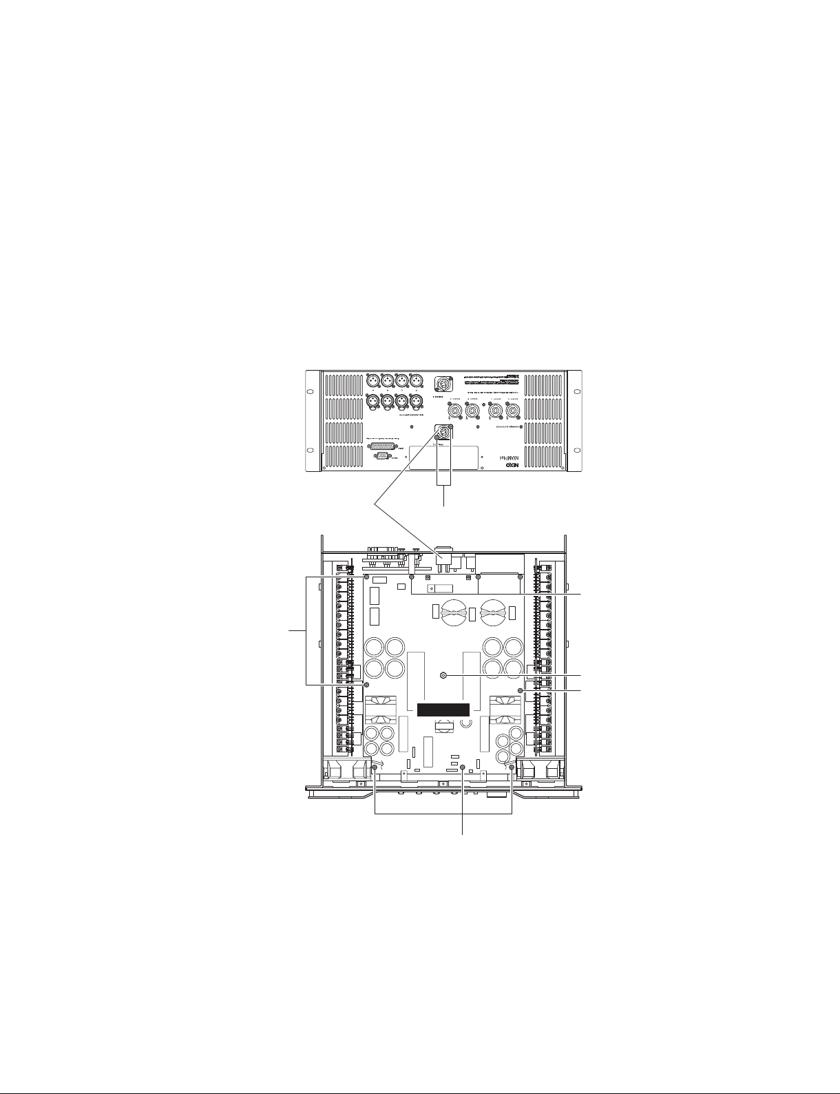
18. Power switch
(Time required: about 25 minutes)
18-1. Remove the top cover and the NX-DFLT card.
(See procedure 1.)
18-2. Remove the CONTROL circuit Board and the OPT
angle. (See procedure 2.)
18-3. Disconnect the power switch connector assembly from
to the PSANHA circuit board.
18-4. Remove the PSANHA circuit Board. (See procedure 3.)
18-5. Disconnect the power switch connector assembly from
the PSANHB circuit board. (Fig. 12)
18-6. Remove the front panel assembly. (See procedure 12.)
18-7. Release the four (4) hooks of the power switch. The
power switch can be removed from the front panel
assembly. (Fig. 12)
Front panel assembly
(フロントパネルAss'y)
18. 電源スイッチ(所要時間:約 25 分)
18-1. トップカバー、NX-DFLT カードを外します。
(1 項参照)
18-2. CONTROL シート、OPT アングルを外します。
(2 項参照)
18-3. PSANHA シートから電源スイッチ Ass'y の線材を外
します。(図 12)
18-4. PSANHA シートを外します。(3 項参照)
18-5. PSANHB シートから電源スイッチ Ass'y の線材を外
します。(図 12)
18-6. フロントパネル Ass'y を外します。(12 項参照)
18-7. 4 箇所のフックを解除し、フロントパネル Ass'y から
電源スイッチを外します。(図 12)
[660]
Power switch
(電源スイッチ)
Hook
(フック)
HookHook
(フック)
[660]: FLAT HEAD SCREW 4x8 MFZN2B3 (--)
Power switch
(電源スイッチ)
Fig. 12
[660]
小ネジ+ FLAT
(図 12)
36
Page 37

NXAMP4x4
LSI PIN DESCRIPTION
■
PCM1803ADBR (X7357B0) A/D CONVERTER
•
PIN
NO.
1V
2V
3V
4V
5V
NAME I/O FUNCTION
IN
L I Analog input, L-channel
IN
R I Analog input, R-channel
REF
1 – Reference voltage 1 decoupling capacitor
REF
2 – Reference voltage 2 decoupling capacitor
CC
– Analog power supply, 5 V
(LSI 端子機能表)
CONTROL: IC035, IC036, IC037, IC038
6 AGND – Analog GND
7
PDWN I Power-down control, active-low
(2)
8 BYPAS I HPF bypass control / LOW: Normal mode (dc reject); HIGH: Bypass mode (through)
9 TEST I Test, must be connected to DGND
10 LRCK I/O Audio data latch enable input/output
11 BCK I/O Audio data bit clock input/output
(2)
(1)
(1)
12 DOUT O Audio data digital output
13 DGND – Digital GND
14 V
DD
15 SCKI I System clock input: 256 fs, 384 fs, 512 fs or 768 fs
16 OSR I Oversampling ratio select input / LOW: x 64 fs, HIGH: x 128 fs
17 FMT0 I Audio data format select input 0 / See data format section
18 FMT1 I Audio data format select input 1 / See data format section
19 MODE0 I Mode select input 0 / See data format section
20 MODE1 I Mode select input 1 / See data format section
– Digital power supply, 3.3 V
(3)
(2)
(2)
(2)
(2)
(2)
(2)
(1) Schmitt trigger input
(2) Schmitt trigger input with internal pulldown (50 kΩ, typically), 5 V tolerant
(3) Schmitt trigger input, 5 V tolerant
37
Page 38

NXAMP4x4
IC BLOCK DIAGRAM
■
r74HCT273PW,118 (X8681A0)
D-type Flip Flop
PN-AN: IC002, 003
D0
QD
CP
MR
GND
1
20
V
2
Q0
3
D0
4
D1
5
Q1
6
Q2
7
D2
8
D3
9
Q3
10
CC
19
Q7
18
D7
CP
17
D6
16
Q6
MR
15
Q5
14
D5
13
D4
12
Q4
11
CP
FF1
Q
R
D
Q0
D4
QD
CP
FF5
Q
R
D
Q4
(IC ブロック図)
D1
D5
D2
QD
CP
FF2
Q
R
D
Q1
D6
QD
CP
FF6
Q
R
D
Q5
D3
QD
CP
FF3
Q
R
D
QD
CP
FF7
Q
R
D
QD
CP
FF4
Q
R
D
Q2
Q6
Q3
D7
QD
CP
FF8
Q
R
D
Q7
r74LVC169PW,118 (X8482A0)
Binaly Counter
CONTROL: IC044, 045
3
DC
U/D
CEP
GND
CP
D0
D1
D2
D3
V
1
16
CC
TC
2
15
Q0
3
14
Q1
4
13
5
12
Q2
6
11
Q3
7
10
CET
4
8
D1
9
PE
5
D2
6
D3
9
PE
7
CEP
10
CET
2
CP
1
U/D
Q
D
CP
Q
Q
D
CP
Q
Q
D
CP
Q
Q
D
CP
Q
14
Q0
13
Q1
12
Q2
11
Q3
15
TC
r74HCT4514PW,118 (X8630A0)
Decoder
PN-AN: IC004-007
A
0
V
24
CC
23
E
A
22
3
21
A
2
20
19
18
17
16
15
14
13
A
Q
1
10
Q
11
Q
8
Q
9
Q
14
Q
15
Q
A
12
2
Q
13
A
3
LE
GND
1
LE
A
2
0
A
3
1
Q
4
7
Q
5
8
Q
6
5
Q
7
4
Q
8
3
Q
9
1
Q
10
2
Q
11
0
12
latch
latch
latch
latch
rCS3318-CQZ (X8486A0)
Volume Controller
CONTROL: IC001
REFO1
OUT1
OUT2
REFO2
IN2
VA-
VA+
Q
0
S
D
Q
1
Q
R
D
S
D
Q
2
Q
R
D
S
D
Q
3
Q
R
D
S
D
Q
4
Q
R
D
E
Q
1
Q
2
Q
3
Q
4
Q
5
Q
6
Q
7
Q
8
Q
9
Q
10
Q
11
Q
12
Q
13
Q
14
Q
15
8-channel
Analog
Inputs
I2C/SPI
Serial
Control
REFI1
RESET
MUTE
SCL/CCLK
SDA/MOSI
AD0/CS
ENOut
DGND
REFI8
8V to 9V
+3.3V
4847464544434241403938
1
IN1
2
3
4
5
6
7
8
9
VD
10
11
IN8
12
1314151617181920212223
OUT8
REFO8
5
I2C/SPI
Control
Port
VA+
VA-
OUT7
Zero Crossing
Detector
REFO7
IN7
REFI2
REFI7
REFI3
REFI8
OUT3
REFO3
IN3
37
36
VA-
35
VA+
34
OUT5
33
REFO4
32
IN4
31
REFI4
30
REFI5
29
IN5
REFO5
28
OUT5
27
VA-
26
VA+
25
24
IN6
OUT6
REFO6
8-channel
3
Analog
Outputs
38
Page 39

NXAMP4x4
rCS4272-CZZR (X8487A0)
CODEC
CONTROL: IC012, 013
3.3V to 5V2.5V to 5V
Hardware or
I2C/SPI
Control Data
Reset
Serial
Audio
Intput
Serial
Audio
Output
Registor/Hardware
Level Translator Level Translator
Configuration
Volume
Control
Volume
Control
PCM Serial Interface/Loopback
rIR2110 (X2382A04)
Driver
PSANH: IC302, 303
Selectable
Interpolation
Filter
Mixer
Selectable
Interpolation
Filter
High Pass Filter and
DC Offset Calibration
High Pass Filter and
DC Offset Calibration
Internal Voltage
Reference
Modulator
Modulator
LOW-Latency
Anti-Alias Filter
LOW-Latency
Anti-Alias Filter
5V
Internal
Oscilator
External
Mute Control
Switched Capasito
DAC and Filterr
Switched Capasito
DAC and Filterr
Multibit
Oversampling
ADC
Multibit
Oversampling
ADC
Left and
Right Mute
Controls
Left
Differential
Output
Right
Differential
Output
Left
Differential
Input
Right
Differential
Input
rDSPB56371AF180 (X8489A0)
DSP
CONTROL: IC022, 023
5
SHI
Interface
2
EXTAL
RESET
PINIT/NMI
212
DAX
Address
Generation
Unit
Six Channel
DAM Unit
Bootstrap
ROM
Internal
Data
Bus
Switch
Clock
Gen-
erator
Triple
Timer
PLL
ESAI
Interface
12
ESAI_1
Interface
PIO_EB
Program
Interruput
Controller
11
GPIO
Peripheral
Expansion Area
Program
Decode
Controller
MODA/IRQA
MODB/IRQB
MODC/IRQC
MODD/IRQD
EFCOP
Program
Address
Controller
Memory Expansion Area
Program
RAM
4K x 24
ROM
64K x 24
YAB
PM_EB
XAB
PAB
DAB
24-Bit
DSP56300
Core
DDB
YDB
XDB
PDB
GDB
24 x 24+56 56-bit MAC
Two 56-bit Accumulators
X Data
RAM
36K x 24
ROM
32K x 24
XM_EB
Data ALU
56-it barrel Shifter
Y Data
RAM
48K x 24
ROM
32K x 24
YM_EB
Power
Mngmnt.
JTAG
OnCE
4
TM
COM
VCC
1
LO
2
3
4
5
VS
6
VB
HO
7
14
13
VSS
12
LIN
11
SD
10
HIN
9
VDD
8
rLD1117STR (X8495A0)
Regulator
CONTROL: IC024
VOLTAGE
GENERATOR
CURRENT
GENERATOR
VB
HV
UV
9
VDD
10
HIN
11
SD
LIN
12
VSS
13
Q
R
S
S
Q
R
VDD/VCC
LEVEL
SHIFT
VDD/VCC
LEVEL
SHIFT
PULSE
PULSE
GEN
GEN
LEVEL
SHIFT
DETECT
PULSE
FILTER
UV
DETECT
DELAY
R
Q
R
S
6
7
HO
5
VS
3
CC
V
LO
1
2
COM
rMAX3221CPWR (X2757A0)
RS-232C Driver
CONTROL: IC041
V
IN
C1+
C1–
C2+
C2–
RIN
EN
1
2
3
V+
4
5
6
7
V–
8
16
15
14
13
12
11
10
9
FORCEOFF
V
CC
GND
DOUT
FORCEON
DIN
INVALID
ROUT
DIN
11
13
DOUT
THERMAL
COMPENSATION
THERMAL
PROTECTION
FORCEOFF
16
12
V
OUT
FORCEON
ROUT
GND
Auto-powerdown
9 8
10
1
INVALID
RIN
EN
39
Page 40

NXAMP4x4
rMX25L1605AM2C-12G (X8718A0) (X8718B0)
Flash Memory
CONTROL: IC039
1
CS#
SCLK
CS#
2
SO
WP#
3
4
GND
Address
Generator
SI
Data
Register
SRAM
Buffer
Mode
Logic
Clock Generator
State
Machine
8
7
6
5
X-Decoder
Memory Array
VCC
HOLD#
SCLK
SI
Page Buffer
Y-Decoder
HV
Generator
Sense
Amplifire
Output
Buffer
SO
REFERENCE
r/+.65&(X6770A0)
SHUNT Regulator
PAANH: IC401
PSANH: IC204
REFERENCE (R)
ANODE
(A)
CATHODE
(K)
CATHOD
ANODE
rNJM2068M-D (X3505A0)
Operational Amplifier
CONTROL: IC002-005, 008-011, 018-021, 028-034
INANH: IC701, 702
OUTANH: IC801, 802
+-
8
7
6
5
+DC Voltage
8
+V
Supply
7
Output B
Inverting
6
Input B
Non-Inverting
5
Input B
+DC Voltage
Supply
Output B
Inverting
Input B
Non-Inverting
Input B
r/+.'"(XD853A0)
Regulator +15V
PSANH: IC202, 203
1
Output A
Inverting
2
Input A
Non-Inverting
Input A
-DC Voltage Supply
+-
3
4
-V
r/+.75&(XR532A0)
Operational Amplifier
CONTROL: IC047, 048, 050, 052
1
Output A
Inverting
Input A
Non-Inverting
Input A
Ground
2
3
4-V
+V
+-
+-
rNJM79M09DL1A (X5366A0)
Regulator
CONTROL: IC007
R1
Q3
Q4
Q10
R2
D2D1
Q6
Q2
R6
Q1
Q7
Q12
R3
Q5
R4
R5
Q17
Q9
Q8
R7
R9R8
Q11
Q13
Q14
Q15
R10
Q16
Q23
Q19
C1 C2
Q18
r/+..%-"(XZ940A0)
Regulator
CONTROL: IC006
INPUT
OUTPUT
COMMON
R22
R20
C3
Q24
R23
R24
Q25
Q20
R13
D3
R14
R17
R16R15R21R12R11
OUTPUT
Q21
Q22
R18
R19
INPUT
INPUT
OUTPUT
40
GND
GND
Page 41

NXAMP4x4
rNJU7630-M (X8682A0)
Regulator
PSANH: IC205
V+
1V
Vref
Soft Start
2
ER.AMP
UVLO
Latch
2A
SCP
2k
0.5
A
R
T
1V
1V
67 8
DTC
FB
IN-
SCP
3
4
5
rPQ1CX12H2ZP (X6188A0)
Regulator
PSANH: IC208
1 8
V
IN
Drive
2
V
B
Circuit
Comparator
Over
current
Detection
circuit
Over
Heat
Detection
circuit
Q
R
F/F
S
6, 7
COM
Oscill
ator
fo Conversion
circuit
Voltage
regulator
ON/OFF
circuit
+
-
AMP
Soft
Start
rPCM1803ADBR (X7357B0)
A/D Converter
CONTROL: IC035-038
Delta-Sigma
Modulator
Delta-Sigma
Modulator
DGND
20
MODE1
19
MODE0
18
FMT1
17
FMT0
16
OSR
15
SCKI
14
V
DD
13
DGND
12
DOUT
11
BCK
BCK
LRCK
x 1/64, x 1/128
Decimation
Filter
With
High-Pass Filter
Clock and Timing Control
V
DD
Serial
Interface
Mode/
Format
Control
DOUT
FMT0
FMT1
MODE0
MODE1
BYPAS
TEST
OSR
PDWN
SCKI
1
VINL
2
R
V
IN
3
V
1
REF
4
2
V
0.8V
0.2V
PWM
Buffer
OUT
1
OSC
0.5V
RT
GND
R
T
L
V
IN
1
V
REF
V
2
REF
V
R
IN
REF
V
AGND
PDWN
BYPAS
TEST
LRCK
Reference
5
CC
6
7
8
9
10
Power Supply
AGNDV
CC
rSG2525AN (X8960A0)
PW Modulator
PSANH: IC301
V
REF
OSC.
REF.
REG.
5k
COMP.
TO INTRENAL
CIRCUITRY
OSCILLATOR
V
REF
50A
16
OUTPUT
V
13
U.V.
LOCK
OUT
4
FLIP
FLOP
R
S
PWM
LATCH
S
NOR
NOR
OR
OR
C
OUTPUT A
11
OUTPUT B
14
SG1525A OUTPUT STAGE
V
13
C
OUTPUT A
11
OUTPUT B
14
Vo
V
15
i
12
GROUND
4
ON/OFF
5
+
V
ref
VNCadj
3
SYNC.
DISCHARGE
COMP.
INV.INPUT
N.I.INPUT
SOFT-START
SHUTDOWN
3
R
6
T
C
5
T
7
9
1
ERROR
AMP.
2
8
5k
10
SG1527A OUTPUT STAGE
41
Page 42

NXAMP4x4
rSN74ABT245BNSR (XU009A0)
BUS Transceiver
CONTROL: IC062
GND
1
DIR
2
A1
3
A2
4
A3
5
A4
6
A5
7
A6
8
A7
9
A8
10
20
Vcc
19
OE
18
B1
17
B2
16
B3
15
B4
14
B5
13
B6
12
B7
11
B8
rSN74LV273APWR (X5074A0)
D-type Flip Flop
CONTROL: IC057-061
1
20
CLR
1Q
2Q
3Q
4Q
GND
1D
2D
3D
4D
V
2
3
4
5
6
7
8
9
10
CC
19
8Q
18
8D
7D
7Q
6Q
6D
5D
5Q
CLK
CLK
CLR
17
16
15
14
13
12
11
1D
3
11
1D
C1
R
1
1Q
rSN74LV14APWR (X6688A0)
Inverter
CONTROL: IC063
VCC
14
A6
13
12
Y6
A5
11
10
Y5
9
A4
8
Y4
GND
A1
1
Y1
2
A2
3
Y2
4
A3
5
Y3
6
7
r4/-7"183#64# (X5966A0)
Buffer/Driver
CONTROL: IC055, 056
PN-AN: IC001
1
GND
G1
2
A1
A2
3
4
A3
5
A4
6
A5
A6
7
A7
8
A8
9
10
2D
3D
4D
5D
6D
7D
4
7
8
13
14
1D
1D
1D
1D
C1
C1
R
2
5
2Q
C1
R
R
6
3Q
9
4Q
1D
C1
R
C1
R
12
5Q
6Q
8D
17
18
1D
1D
C1
16 19
7Q
C1
R
8Q
R
15
20
Vcc
19
G2
18
Y1
17
Y2
16
Y3
15
Y4
Y5
14
13
Y6
12
Y7
11
Y8
rSN74LV4052APWR (X6976A0)
Demultiplexer
CONTROL: IC049
10
2Y0
2Y2
2-COM
2Y3
2Y1
INH
GND
GND
V
16
1
CC
1Y2
15
2
1Y1
14
3
1-COM
13
4
5
12
1Y0
6
11
1Y3
7
10
A
8
9
B
A
9
B
6
INH
42
rSN74LVC00APWR (X5406A0)
NAND
13
1-COM
12
1Y0
14
1Y1
15
1Y2
11
1Y3
1
2Y0
5
2Y1
2
2Y2
4
2Y3
3
2-COM
CONTROL: IC040
1B 2
1Y 3
2A 4
2B 5
2Y 6
GND 7
Vcc141A 1
4B13
4A12
4Y11
3B10
3A9
3Y8
Page 43

NXAMP4x4
rSN74LVC157APWR (X6786A0)
Data Selector
CONTROL: IC046, 051
1A
2
1B
3
CC
2A
5
2B
6
3A
11
3B
10
4A
14
4B
13
G
15
A/B
1
GND
A/B
1A
1B
1Y
2A
2B
2Y
G
15
2
4A
14
3
4B
13
4
5
12
4Y
6
11
3A
7
10
3B
8
9
3Y
V
16
1
rSN74LVC2G74DCTR (X8709A0)
Flip Flop
CONTROL: IC042
PRE
7
CLK
1
D
2
CLR
6
C
C
C
TG
C
C
TG
C
C
TG
C
rSN74LVC245APWR (XZ287A0)
Bas Transceiver
CONTROL: IC054
1
DIR
1Y
4
7
2Y
3Y
9
4Y
12
Q
5
C
TG
Q
C
3
GND
2
A1
3
A2
4
A3
5
A4
6
A5
7
A6
8
A7
9
A8
10
20
Vcc
19
OE
18
B1
17
B2
16
B3
15
B4
14
B5
13
B6
12
B7
11
B8
rTC74LCX04FT (X8415A0)
Inverter
CONTROL: IC064
VCC
14
6A
13
12
6Y
5A
11
10
5Y
9
4A
8
4Y
GND
1A
1
1Y
2
2A
3
2Y
4
3A
5
3Y
6
7
r501:/1% (X8576A0)
Regulator
PSANH: IC201
CONTROL (1C)
EXTERNAL
CURRENT LIMIT (3X)
LINE-SENSEL (2L)
FREQUENCY (5F)
Z
C
SHUNT REGULATOR/
ERROR AMPLIFIER
I
FB
CURRENT
LIMIT
ADJUST
LINE
SENSE
R
E
V
BG+VT
V
BG
V
C
V
ON/OFF
1 V
5.0V
I(LIMIT)
SOFT
START
OVAIV
DC
MAX
6.8V
4.6V
INTERNAL UV
COMPARATOR
STOP LOGIC
STOP
DC
MAX
HALF
FREQ
OSCILLATOR WITH JITTER
SOFTSTART
D
CLOCK
MAX
SAW
SOFT START
LIQHT LOAD
FREQUENCY
REDUCTION
+8
SHUTDOWN
AUTO-RESTART
HYSTERETIC
THERMAL
SHUTDOWN
PWM
COMPARATOR
0
1
INTERNAL
SUPPLY
DRAIN (7D)
Tab internally
connected to
SOURCE pin
CURRENT LIMIT
COMPARATOR
CONTROLLED
TURN-ON
GATE DRIVER
Q
S
R
LEADING
EDGE
BLANKING
2L
5F
3X
4S
1C
7D
SOURCE (4S)
43
Page 44

NXAMP4x4
■ CIRCUIT BOARDS
(シート基板図)
CONTENTS
• CONTROL Circuit Board (X8710D0) ............................ 46
• INANH Circuit Board (X8714C0) ............................ 45
• LCD SPACER Circuit Board (X8711E0) ............................62
• NX-DFLT Circuit Board (YC233A0) ............................63
• OPT-AN Circuit Board (X8711E0) ............................62
• OUTANH Circuit Board (X8714C0) ............................ 50
• PAANH Circuit Board (X8712G0) ............................56
• PN-AN Circuit Board (X8711E0) ............................52
• PSANHA, PSANHB Circuit Board (X8715G0) ............................58
• RS232-GPI Circuit Board (X8711E0) ............................62
Note: See parts list for details of circuit board component parts.
注: シートの部品詳細はパーツリストをご参照ください。
(目次)
44
Page 45

• INANH Circuit Board
NXAMP4x4
to CONTROL
CN006
DCBA
BALANCED INPUTS
Component side
(部品側)
2NA-WJ97320-10
Pattern side
0
(パターン側)
45
Page 46

NXAMP4x4
• CONTROL Circuit Board
A
to PN-AN
CN001
to PSANHB
CN313
to PSANHA
CN313
to PSANHA
CN201
to OUTANH
CN809, CN810
46
Component side
(部品側)
A'
2NA-WR77020-10
0
Page 47

A
• CONTROL Circuit Board
A
NXAMP4x4
to OUTANH
CN809, CN810
to PAANH
(CH1)
CN401
to PAANH
(CH2)
CN401
to PAANH
(CH3)
CN401
to PAANH
(CH4)
CN401
to INANH
W701
to OPT-AN
CN301
A'
2NA-WR77020-10
to RS232-GPI
CN201
Component side
0
(部品側)
47
Page 48

NXAMP4x4
• CONTROL Circuit Board
B
48
Pattern side
(パターン側)
B'
2NA-WR77020-10
0
Page 49

• CONTROL Circuit Board
B
NXAMP4x4
B'
2NA-WR77020-10
Pattern side
0
(パターン側)
49
Page 50

NXAMP4x4
• OUTANH Circuit Board
to PAANH (CH4)
W405 (ORANGE)
to PAANH (CH3)
W405 (ORANGE)
to PAANH (CH2)
W405 (ORANGE)
to PAANH (CH1)
W405 (ORANGE)
to PSANH
CN202
to CONTROL
to CONTROL
CN016
CN016
50
to PSANHB
CN317
CN317
to PSANHA
Component side
Speakon D Speakon C Speakon B Speakon A
POWER OUTPUTS
(部品側)
to PSANHB
to PSANHA
2NA-WJ97320-10
CN306
CN306
0
Page 51

• OUTANH Circuit Board
NXAMP4x4
2NA-WJ97320-10
Pattern side
0
(パターン側)
51
Page 52

NXAMP4x4
• PN-AN Circuit Board
A
SELECT
PEAK
PROTECT
SIGNAL
Component side
(部品側)
1
MUTE
23
MUTE MUTE
52
A'
2NA-WJ97170-10
2
Page 53

• PN-AN Circuit Board
A
NXAMP4x4
Encoder
4A
vol
MUTE
B
to CONTROL
CN009
Component side
AMP PROTECT
STAND-BY
POWER
(部品側)
A'
2NA-WJ97170-10
2
53
Page 54

NXAMP4x4
• PN-AN Circuit Board
B
54
Pattern side
(パターン側)
B'
2NA-WJ97170-10
2
Page 55

• PN-AN Circuit Board
B
NXAMP4x4
B'
2NA-WJ97170-10
Pattern side
2
(パターン側)
55
Page 56

NXAMP4x4
• PAANH Circuit Board
to CONTROL
CN012, CN013, CN014, CN015
CN805, CN806, CN807, CN808
to OUTANH
to PSANH
CN312, CN315
A
A'
Component side
(部品側)
B
56
Pattern side
(パターン側)
2NA-WR77710-20
B'
1
Page 57

• PAANH Circuit Board
A
NXAMP4x4
A'
to PSANH CN307, CN310
to PSANH CN316, CN309
to PSANH CN305, CN308
Component side
(部品側)
B
B'
2NA-WR77710-20
Pattern side
1
(パターン側)
57
Page 58

NXAMP4x4
• PSANHA, PSANHB Circuit Board
to PAANH
to OUTANH W802, W803
to PAANH W404
to PAANH W402
to PAANH W401
to FUN
to CONTROL CN007, CN008
Reduction: 7/10
A
W403
to OUTANH W801
to CONTROL CN011
to PSANHB CN203
to FUN
to PAANH W401
to PAANH W402
to PAANH W404
to PAANH W403
to OUTANH
W804, W805
6
7
5
8
4
9
3
10
2
11
1
12
58
Component side
(部品側)
B'
2NA-WJ97350-70
3
Page 59

NXAMP4x4
• PSANHA, PSANHB Circuit Board
A
Reduction: 7/10
B'
2NA-WJ97350-70
Component side
3
(部品側)
59
Page 60

NXAMP4x4
• PSANHA, PSANHB Circuit Board
Reduction: 7/10
B
60
Pattern side
(パターン側)
B'
2NA-WJ97350-70
3
Page 61

NXAMP4x4
• PSANHA, PSANHB Circuit Board
B
Reduction: 7/10
7
6
8
5
9
4
10
3
11
2
12
1
B'
2NA-WJ97350-70
Pattern side
3
(パターン側)
61
Page 62

NXAMP4x4
• RS232-GPI Circuit Board
to CONTROL CN010
RS232
GPIO
• OPT-AN Circuit Board
Component side
(部品側)
to CONTROL CN017
Expansion slot
Component side
Pattern side
(部品側)
(パターン側)
• LCD SPACER Circuit Board
Component side
62
(部品側)
Pattern side
Pattern side
(パターン側)
(パターン側)
2NA-WJ97320-10
0
Page 63

• NX-DFLT Circuit Board
NXAMP4x4
Expansion
slot
Component side
(部品側)
2NA-WT66120-10
Pattern side
0
(パターン側)
63
Page 64

NXAMP4x4
TEST PROGRAM
■
1. Required items
Computer : DOS/V computer x1 (Pentium 200MHz or more, Windows XP, USB Port)
Software : Software for version up (JTAG Programmer)
Cable : RLINK-ST (USB-JTAG adapter)
Measuring equipment : Power consumption meter
Tools : RS-232C jig x1, GPI jig x1, SLOT jig x1
RS-232C jig
D-SUB 9 pin female connector
GPI jig
SW1
D-SUB 25 pin male connector
/ETH_CS
/ES_CS
SPI_CLK
SPI_MISO
SPI_MOSI
ES_SERIAL_RX
ES_SERIAL_TX
INT_FROM_ES
ES_GPI1
ES_GPI2
ES_GPI3
ES_I2S_DATA0
ES_I2S_DATA1
ES_MCLK
ES_SCLK
ES_LRCK
SOURCE_SEL
a-1
b-1
a-40 b-40
SLOT jig
3.3D
3.3D
XTAL
12.288MHz
Q0
Q1
LV1 69
Q2
Q3
Q0
Q1
LV1 69
Q2
Q3
2. Test connection image
64
SLOT, GPI, RS-232C jig
NXAMP
Measuring
instrument
Page 65

3. Operation
3-1. Entry of the test program
While holding down the [SELECT4], [MUTE4] and [A]
buttons simultaneously, turn the power switch on. The
start up screen appears on the LCD.
Start Up Screen
NXAMP4x4
Press the switch displayed on the LCD as instructed one
by one.
If all instructed switches are OK, the display automatically returns to the test menu screen.
4-2. ENCODER test
Boot1.29
WAIT...
Then release your fingers from the buttons.
The test program starts and the test menu screen appears on the LCD display.
Test Menu Screen
00CHOOSETEST<>
01SWITCH
3-2. Executing the test and judgment display
Select the desired test item from the table below using
the rotary encoder, and press the [B] button to start the
test.
Test Items List
01 SWITCH
02 ENCODER
03 LED
04 LCD
05 RS232
06 GPI
07 PORT (no use)
08 DSP
09 WORD CLOCK
10 12C
11 FLASH
12 FAN
13 SLOT
14 ATTENUATION
15 ANALOG
16 BRIDGE
17 CALIBRATION
18 STANDBY
19 QUIT
After executing the test, the display returns to the test
menu screen if the test result is OK. If an error occurs,
“ERROR” appears on the LCD and the test program is
stopped. In that case, turn the power switch off and on
again as was done above in 3-1.
4. Outline of tests
4-1. SWITCH test
00CHOOSETEST<>
02ENCODER
Press the [B] button to start the test. The following display appears.
02ENCODER
TURNRIGHT0
Turn the ENCODER knob clockwise. The 2nd line on the
display changes as shown below.
TURN RIGHT 0 –> • • • • • –> TURN RIGHT 19
The following display appears after the 2nd line on the
display reaches TURN RIGHT 19.
02ENCODER
TURNLEFT0
Turn the ENCODER knob counterclockwise. The 2nd
line on the display changes as shown below.
TURN LEFT 0 –> • • • • • –> TURN LEFT 19
The display returns to the test menu screen after the 2nd
line on the display reaches TURN LEFT 19.
4-3. LED test
00CHOOSETEST<>
03LED
Press the [B] button to start the test. The following display appears.
03LED
00CHOOSETEST<>
01SWITCH
Press the [B] button to start the test. The LCD shows one
by one the switch name to be tested as shown below.
01SWITCH
HITSELECTCH1
The LEDs automatically light up one by one in a specific
order as shown on the next page.
All LEDs will light at the same time after each LED individually has been tested. Confirm that each LED is lit
normally. If OK, press the [B] button to return the display
to the test menu screen.
65
Page 66

NXAMP4x4
Lighting order
4-4. LCD test
00CHOOSETEST<>
04LCD
Press the [B] button to start the test.
First the following display appears.
Press the [B] button to continue the test. The test is executed automatically.
After executing the test, the following display appears.
(When an error occurs, “ERROR” appears and the test
program is stopped.)
04LCD
All the dots of the LCD go on and off two times. Finally,
all the dots of the LCD are lit. Confirm that all the dots of
the LCD have lit normally. If OK, press the [B] button to
return the display to the test menu screen.
4-5. RS-232C test
00CHOOSETEST<>
05RS-232C
Connect the RS-232C jig to the R232C port of this unit.
Press the [B] button to start the test. The following display appears.
05RS-232C
RS-232COK?
05RS-232C
RELEASERS-232C
Disconnect the RS-232C jig from the RC232C port of
this unit. Press the [B] button to return the display to the
test menu screen.
4-6. GPI test
00CHOOSETEST<>
06GPI
Connect the GPI jig to the GPIO port of this unit.
Then press the [B] button to start the test. The following
display appears.
06GPI
GPO[0:4]TESTOK?
Switch the GPI jig to the GPO [0:4] position and press
the [B] button to continue the test.
The test executes automatically.
If normal, the following display appears. (If an error
occurs, “ERROR” appears and the test program is
stopped.)
66
06GPI
GPO[5:7]TESTOK?
Page 67

NXAMP4x4
Switch the GPI jig to the GPO [5:7] position. Press the [B]
button to continue the test.
The test executes automatically. If the test result is
OK, the display automatically returns to the test menu
screen. (If an error occurs, “ERROR” appears and the
test program is stopped.)
Disconnect the GPI jig from the GPIO port.
4-7. PORT test
Test for factory inspection only.
4-8. DSP test
00CHOOSETEST<>
08DSP
Press the [B] button to start the test. The following display appears.
08DSP
CPUtoDSPTESTOK?
Press the [B] button to continue the test. The test executes automatically.
If normal, the following display appears.
Press the [B] button to start the test. The following display appears.
09WORDCLOCK
LRCK48kTESTOK?
Press the [B] button to continue the test. The test executes automatically.
If normal, the following display appears.
09WORDCLOCK
LRCK96kTESTOK?
Press the [B] button to continue the test. The test executes automatically.
If the test result is OK, the display automatically returns
to the test menu screen.
(If an error occurs, “ERROR” appears and the test program is stopped.)
4-10. 12C test
00CHOOSETEST<>
1012C
08DSP
DSPtoDSPTESTOK?
Press the [B] button to continue the test. The test executes automatically.
If the test result is OK, the display automatically returns
to the test menu screen.
(If an error occurs, “ERROR” appears and the test program is stopped.)
4-9. WORD CLOCK test
00CHOOSETEST<>
09WORDCLOCK
Press the [B] button to start the test. The following display appears.
1012C
12CTESTOK?
Press the [B] button to continue the test. The test executes automatically.
If the test result is OK, the display automatically returns
to the test menu screen.
(If an error occurs, “ERROR” appears and the test program is stopped.)
67
Page 68

NXAMP4x4
4-11. FLASH test
00CHOOSETEST<>
11FLASH
Press the [B] button to start the test. The following display appears.
11FLASH
FLASHTESTOK?
Press the [B] button to continue the test. The test executes automatically.
If the test result is OK, the display automatically returns
to the test menu screen.
(If an error occurs, “ERROR” appears and the test program is stopped.)
4-12. FAN test
00CHOOSETEST<>
12FAN
Press the [B] button to start the test. The following display appears.
The FAN starts rotating at low speed.
12FAN
LOW
Check that the FAN rotates at low speed, and press the
[B] button to continue the test. The following display appears, and the FAN rotates at middle speed.
12FAN
MIDD
4-13. SLOT test
00CHOOSETEST<>
13SLOT
Rear panel
Expansion slot
(Turn off the power to this unit, and insert the SLOT jig
into the expansion slot. Restart the test program, and
select this test.)
Press the [B] button to start the test. The test executes
automatically.
If every signal is normal, the following display appears
and the LED of the SLOT jig lights.
(If an error occurs, “ERROR” appears and the test program is stopped.)
13SLOT
ANALOGTESTOK?
Input the 1 kHz, -10 ±1 dBu sine wave to the channel
1 input terminal and confirm that the output voltage
obtained at the channel 1 output terminal is +24.1 ±2.0
dBu.
If OK, press the [B] button to return the display to the
test menu screen.
4-14. ATTENUATION test
68
Check that the FAN rotates at middle speed, and press
the [B] button to continue the test. The following display
appears, and the FAN rotates at high speed.
12FAN
HIGH
Check that the FAN rotates at high speed, and press the
[B] button to return the display to the test menu screen.
00CHOOSETEST<>
14ATTENUATION
Press the [B] button to enter the attenuation test mode.
The following display appears.
14ATTENUATION
NOISETESTOK?
Perform the test according to the “Inspection with attenuation test mode”. (See page 79).
If OK, press the [B] button to return the display to the
test menu screen.
Page 69

4-15. ANALOG test
00CHOOSETEST<>
15ANALOG
Press the [B] button to enter the analog test mode. The
following display appears.
15ANALOG
ANALOGTESTOK?
Perform the test according to the “Inspection with analog
test mode”. (See page 79–81)
Press the [B] button. The following display appears.
15ANALOG
MUTETESTOK?
If OK, press the [B] button to return the display to the
test menu screen.
4-16. BRIDGE test
00CHOOSETEST<>
16BRIDGE
Press the [B] button to enter the bridge test mode. The
following display appears.
16BRIDGE
ANALOGTESTOK?
Perform the test according to the “Inspection with
BRIDGE mode”. (See page 82)
If OK, press the [B] button to return the display to the
test menu screen.
4-17. CALIBRATION
00CHOOSETEST<>
17CALIBRATION
Press the [B] button to start the calibration. The following
display appears.
17CALIBRATION
CH1INPUTSIGNALOK?
Input the 1 kHz, +10 dBu sine wave to the channel 1 input terminal, and press the [B] button. The analog input
level is automatically calibrated, and the following display appears.
17CALIBRATION
CH2INPUTSIGNALOK?
NXAMP4x4
Input the 1 kHz, +10 dBu sine wave to the channel 2 input terminal, and press the [B] button. The analog input
level is automatically calibrated, and the following display appears.
17CALIBRATION
CH3INPUTSIGNALOK?
Input the 1 kHz, +10 dBu sine wave to the channel 3 input terminal, and press the [B] button. The analog input
level is automatically calibrated, and the following display appears.
17CALIBRATION
CH4INPUTSIGNALOK?
Input the 1 kHz, +10 dBu sine wave to the channel 4 input terminal, and press the [B] button. The analog input
level is automatically calibrated, and the following display appears.
17CALIBRATION
CH1SETTO38.1dBu?
Input the 1 kHz, +10 dBu sine wave to the channel 1 input terminal.
Adjust the ENCODER so that the output voltage obtained at the channel 1 output terminal is +38.1 dBu,
and press the [B] button.
The analog output level is automatically calibrated, and
the following display appears.
17CALIBRATION
CH2SETTO38.1dBu?
Input the 1 kHz, +10 dBu sine wave to the channel 2 input terminal.
Adjust the ENCODER so that the output voltage obtained at the channel 2 output terminal is +38.1 dBu,
and press the [B] button.
The analog output level is automatically calibrated, and
the following display appears.
17CALIBRATION
CH3SETTO38.1dBu?
Input the 1 kHz, +10 dBu sine wave to the channel 3 input terminal.
Adjust the ENCODER so that the output voltage obtained at the channel 3 output terminal is +38.1 dBu,
and press the [B] button.
The analog output level is automatically calibrated, and
the following display appears.
17CALIBRATION
CH4SETTO38.1dBu?
69
Page 70

NXAMP4x4
70
Input the 1 kHz, +10 dBu sine wave to the channel 4 input terminal.
Adjust the ENCODER so that the output voltage obtained at the channel 4 output terminal is +38.1 dBu,
and press the [B] button.
The analog output level is automatically calibrated, and
the following display appears.
17CALIBRATION
CH1OUTPUTSIGNALOK?
Adjust the input signal voltage so that the output voltage
obtained at the channel 1 output terminal is 40 Vrms (=
+34.3 dBu), and press the [B] button.
The output voltage monitor is automatically calibrated,
and the following display appears.
17CALIBRATION
CH2OUTPUTSIGNALOK?
Adjust the input signal voltage so that the output voltage
obtained at the channel 2 output terminal is 40 Vrms (=
+34.3 dBu), and press the [B] button.
The output voltage monitor is automatically calibrated,
and the following display appears.
17CALIBRATION
CH3OUTPUTSIGNALOK?
Adjust the input signal voltage so that the output voltage
obtained at the channel 3 output terminal is 40 Vrms (=
+34.3 dBu), and press the [B] button.
The output voltage monitor is automatically calibrated,
and the following display appears.
17CALIBRATION
CH4OUTPUTSIGNALOK?
Adjust the input signal voltage so that the output voltage
obtained at the channel 4 output terminal is 40 Vrms (=
+34.3 dBu), and press the [B] button.
The output voltage monitor is automatically calibrated,
and the following display appears.
17CALIBRATION
CH1CONNECT8OHMLOAD
Connect the 8 Ω resistor to the channel 1 output terminal.
Adjust the input signal voltage so that the output voltage
obtained at the channel 1 output terminal is 40 Vrms (=
+34.3 dBu), and press the [B] button.
The output current monitor is automatically calibrated,
and the following display appears.
17CALIBRATION
CH2CONNECT8OHMLOAD
Connect the 8 Ω resistor to the channel 2 output terminal.
Adjust the input signal voltage so that the output voltage
obtained at the channel 2 output terminal is 40 Vrms (=
+34.3 dBu), and press the [B] button.
The output current monitor is automatically calibrated,
and the following display appears.
17CALIBRATION
CH3CONNECT8OHMLOAD
Connect the 8 Ω resistor to the channel 3 output terminal.
Adjust the input signal voltage so that the output voltage
obtained at the channel 3 output terminal is 40 Vrms (=
+34.3 dBu), and press the [B] button.
The output current monitor is automatically calibrated,
and the following display appears.
17CALIBRATION
CH4CONNECT8OHMLOAD
Connect the 8 Ω resistor to the channel 4 output terminal.
Adjust the input signal voltage so that the output voltage
obtained at the channel 4 output terminal is 40 Vrms (=
+34.3 dBu), and press the [B] button.
The output current monitor is automatically calibrated,
and the display returns to the test menu screen.
(If an error occurs, “ERROR” appears and the test program is stopped.)
4-18. STANDBY test
00CHOOSETEST<>
18STANDBY
Press the [B] button to enter the standby mode. The following display appears.
18STANDBY
Measure the primary power consumption, and check
that the measured value is 23 W or less. Press the [B]
button for one second or more, and the display returns
to the test menu screen.
4-19. QUIT (Exit the test program)
00CHOOSETEST<>
19QUIT
Press the [B] button to exit the test program. This unit
enters the ordinary mode.
Page 71

テストプログラム
■
1. 必要なもの
パソコン :DOS/V パソコン(Pentium200MHz 以上、WindowsXP、USB ポート)
ソフトウェア :バージョンアップ用ソフトウェア (JTAGProgrammer)
ケーブル :RLINK-ST(USB-JTAG アダプター)
測定器 :消費電力計
冶具 :RS-232C 冶具x1、GPI 冶具x1、SLOT 冶具x1
NXAMP4x4
RS-232C 冶具
D-SUB9 ピンメスコネクター
GPI 冶具
SW1
D-SUB9 ピンオスコネクター
/ETHCS
/ESCS
SPICLK
SPIMISO
SPIMOSI
ESSERIALRX
ESSERIALTX
INTFROMES
ESGPI1
ESGPI2
ESGPI3
ESI2SDATA0
ESI2SDATA1
ESMCLK
ESSCLK
ESLRCK
SOURCESEL
a-1
b-1
a-40 b-40
スロット冶具
3.3D
Q0
Q1
Q2
Q3
LV169
3.3D
XTAL
12.288MHz
Q0
Q1
LV169
Q2
Q3
2. 接続イメージ
SLOT、GPI、
RS-232C 冶具
NXAMP
測定器
71
Page 72

NXAMP4x4
3. 操作
3-1.テストプログラムの起動
[SELECT4]ボタン、[MUTE4]ボタン、[A]ボタ
ンを同時に押しながら電源スイッチを ON にします。
LCD に起動画面が表示されます。
起動画面
LCD にその名前が表示されたスイッチを1つ1つ押し
ます。
全スイッチが OK であれば、表示は自動的に検査メ
ニュー画面に戻ります。
4-2.エンコーダー検査
Boot1.29
WAIT...
[SELECT4]ボタン、[MUTE4]ボタン、[A]ボタン
を離します。テストプログラムが起動し、検査メニュー
画面が表示されます。
検査メニュー画面
00CHOOSETEST<>
01SWITCH
3-2.検査の実行と検査結果の表示
ロータリーエンコーダーで下記の表から検査項目を選
び、[B]ボタンを押して検査を行います。
検査項目選択リスト
01 SWITCH
02 ENCODER
03 LED
04 LCD
05 RS232
06 GPI
07 PORT (no use)
08 DSP
09 WORD CLOCK
10 12C
11 FLASH
12 FAN
13 SLOT
14 ATTENUATION
15 ANALOG
16 BRIDGE
17 CALIBRATION
18 STANDBY
19 QUIT
00CHOOSETEST<>
02ENCODER
[B]ボタンを押して検査をスタートします。下記の画
面が表示されます。
02ENCODER
TURNRIGHT0
エンコーダーツマミを時計方向に回します。2 行目の表
示が下記のように変化します。
TURNRIGHT0‒>•••••‒>TURNRIGHT19
2 行目の表示が「TURNRIGHT19」になった後、下記
のように表示されます。
02ENCODER
TURNLEFT0
エンコーダーツマミを反時計方向に回します。2 行目の
表示が下記のように変化します。
TURNLEFT0‒>•••••‒>TURNLEFT19
2 行目の表示が「TURNLEFT 19」になった後、表示
は自動的に検査メニュー画面に戻ります。
検査後、検査結果が OK のとき、表示は検査メニュー
画面に戻ります。
エラーが発生した場合、LCD に「ERROR」が表示され、
テストプログラムが停止します。
その場合、電源スイッチを一度 OFF にした後、3-1 の
方法でテストプログラムを再起動します。
4. 検査の概要
4-1.スイッチ入力検査
00CHOOSETEST<>
01SWITCH
[B]ボタンを押して検査をスタートします。
検査するスイッチの名称が1つ1つ下記のように LCD
に表示されます。
01SWITCH
HITSELECTCH1
72
4-3.LED 検査
00CHOOSETEST<>
03LED
[B]ボタンを押して検査をスタートします。下記の画
面が表示されます。
03LED
LED が、次ページに示す順番で1つ1つ自動的に点灯
します。
各 LED の検査後、全 LED が同時に点灯します。各
LED が正常に点灯していることを確認します。
OK であれば、[B]ボタンを押して表示を検査メニュー
画面に戻します。
Page 73

点灯順
4-4.LCD検査
00CHOOSETEST<>
04LCD
[B]ボタンを押して検査をスタートします。
最初に下記の画面が表示されます。
NXAMP4x4
[B]ボタンを押して検査を継続します。検査が自動的
に実施されます。
検査実施後、下記の画面が表示されます。
(エラーが発生した場合、「ERROR」が表示され、テス
トプログラムが停止します。)
04LCD
LCD の全ドットが、点灯/消灯を 2 回繰り返します。
最後に全ドットが点灯します。全ドットが正常に点灯
していることを確認します。
OK であれば、[B]ボタンを押して表示を検査メニュー
画面に戻します。
4-5.RS-232C 検査
00CHOOSETEST<>
05RS-232C
本機の RS232C ポートに RS-232C 冶具を接続します。
[B]ボタンを押して検査をスタートします。下記の画
面が表示されます。
05RS-232C
RS-232COK?
05RS-232C
RELEASERS-232C
本機の RS232C ポートから RS-232C 冶具を外します。
[B]ボタンを押して表示を検査メニュー画面に戻しま
す。
4-6.GPI 検査
00CHOOSETEST<>
06GPI
本機の GPIO ポートに GPI 冶具を接続します。
[B]ボタンを押して検査をスタートします。下記の画
面が表示されます。
06GPI
GPO[0:4]TESTOK?
GPI 冶具を GPO[0:4]ポジションに切り替えて、[B]
ボタンを押して検査を継続します。
検査が自動的に実施されます。
正常であれば、下記の画面が表示されます。(エラーが
発生した場合、「ERROR」が表示され、テストプログ
ラムが停止します。)
06GPI
GPO[5:7]TESTOK?
73
Page 74

NXAMP4x4
GPI 冶具を GPO[5:7]ポジションに切り替えて、[B]
ボタンを押して検査を継続します。
検査が自動的に実施されます。
正常であれば、表示が検査メニュー画面に戻ります。(エ
ラーが発生した場合、「ERROR」が表示され、テスト
プログラムが停止します。)
GPIO ポートから GPI 冶具を外します。
4-7.ポート検査
工場検査専用
4-8.DSP 検査
00CHOOSETEST<>
08DSP
[B]ボタンを押して検査をスタートします。下記の画
面が表示されます。
08DSP
CPUtoDSPTESTOK?
[B]ボタンを押して検査を継続します。検査が自動的
に実施されます。
正常であれば、下記の画面が表示されます。
[B]ボタンを押して検査をスタートします。下記の画
面が表示されます。
09WORDCLOCK
LRCK48kTESTOK?
[B]ボタンを押して検査を継続します。検査が自動的
に実施されます。
正常であれば、下記の画面が表示されます。
09WORDCLOCK
LRCK96kTESTOK?
[B]ボタンを押して検査を継続します。検査が自動的
に実施されます。
検査結果が OK であれば、表示が検査メニュー画面に
戻ります。
(エラーが発生した場合、「ERROR」が表示され、テス
トプログラムが停止します。)
4-10.12C 検査
00CHOOSETEST<>
1012C
08DSP
DSPtoDSPTESTOK?
[B]ボタンを押して検査を継続します。検査が自動的
に実施されます。
検査結果が OK であれば、表示が検査メニュー画面に
戻ります。
(エラーが発生した場合、「ERROR」が表示され、テス
トプログラムが停止します。)
4-9.WORDCLOCK 検査
00CHOOSETEST<>
09WORDCLOCK
[B]ボタンを押して検査をスタートします。下記の画
面が表示されます。
1012C
12CTESTOK?
[B]ボタンを押して検査を継続します。検査が自動的
に実施されます。
検査結果が OK であれば、表示が検査メニュー画面に
戻ります。
(エラーが発生した場合、「ERROR」が表示され、テス
トプログラムが停止します。)
74
Page 75

NXAMP4x4
4-11.FLASH 検査
00CHOOSETEST<>
11FLASH
[B]ボタンを押して検査をスタートします。下記の画
面が表示されます。
11FLASH
FLASHTESTOK?
[B]ボタンを押して検査を継続します。検査が自動的
に実施されます。
検査結果が OK であれば、表示が検査メニュー画面に
戻ります。
(エラーが発生した場合、「ERROR」が表示され、テス
トプログラムが停止します。)
4-12.FAN 検査
00CHOOSETEST<>
12FAN
[B]ボタンを押して検査をスタートします。下記の画
面が表示されます。
ファンが低速で回転します。
12FAN
LOW
ファンが低速で回転することを確認し、[B]ボタンを
押して検査を継続します。
下記の画面が表示され、ファンが中速で回転します。
12FAN
MIDD
ファンが中速で回転することを確認し、[B]ボタンを
押して検査を継続します。
下記の画面が表示され、ファンが高速で回転します。
12FAN
HIGH
ファンが高速で回転することを確認し、[B]ボタンを
押して表示を検査メニュー画面に戻します。
4-13.SLOT 検査
00CHOOSETEST<>
13SLOT
リアパネル
拡張スロット
(本機の電源を切り、拡張スロットに SLOT 冶具を挿入
します。テストプログラムを再起動し、このテストを
選びます。)
[B]ボタンを押して検査をスタートします。検査が自
動的に実施されます。
全ての信号が正常であれば、下記の画面が表示され、
スロット冶具の LED が点灯します。
(エラーが発生した場合、「ERROR」が表示され、テス
トプログラムが停止します。)
13SLOT
ANALOGTESTOK?
チャンネル 1 の入力端子に 1kHz、-10 ±1 dBu の正
弦波を入力し、チャンネル 1 の出力端子に +24.1 ±2.0
dBu の出力が得られることを確認します。
OK であれば、[B]ボタンを押して表示を検査メニュー
画面に戻します。
4-14.ATTENUATION 検査
00CHOOSETEST<>
14ATTENUATION
[B]ボタンを押して ATTENUATION 検査モードに入
ります。
下記の画面が表示されます。
14ATTENUATION
NOISETESTOK?
「アッテネーション検査モードでの検査」にしたがって
検査を行います。(84 ページ参照)
OK であれば、[B]ボタンを押して表示を検査メニュー
画面に戻します。
75
Page 76

NXAMP4x4
4-15.ANALOG 検査
00CHOOSETEST<>
15ANALOG
[B]ボタンを押してアナログ検査モードに入ります。
下記の画面が表示されます。
15ANALOG
ANALOGTESTOK?
「アナログ検査モードでの検査」にしたがって検査を行
います。(85、86 ページ参照)
[B]ボタンを押します。下記の画面が表示されます。
15ANALOG
MUTETESTOK?
OK であれば、[B]ボタンを押して表示を検査メニュー
画面に戻します。
4-16.BRIDGE 検査
00CHOOSETEST<>
16BRIDGE
[B]ボタンを押してブリッジ検査モードに入ります。
下記の画面が表示されます。
16BRIDGE
ANALOGTESTOK?
チャンネル 2 の入力端子に 1 kHz、+10 dBu の正弦波
を入力し、[B]ボタンを押します。アナログ入力レベ
ルが自動的にキャリブレーションされ、下記の画面が
表示されます。
17CALIBRATION
CH3INPUTSIGNALOK?
チャンネル 3 の入力端子に 1 kHz、+10 dBu の正弦波
を入力し、[B]ボタンを押します。アナログ入力レベ
ルが自動的にキャリブレーションされ、下記の画面が
表示されます。
17CALIBRATION
CH4INPUTSIGNALOK?
チャンネル 4 の入力端子に 1 kHz、+10 dBu の正弦波
を入力し、[B]ボタンを押します。アナログ入力レベ
ルが自動的にキャリブレーションされ、下記の画面が
表示されます。
17CALIBRATION
CH1SETTO38.1dBu?
チャンネル 1 の入力端子に 1 kHz、+10 dBu の正弦波
を入力します。
チャンネル1 の出力端子の出力電圧が +38.1 dBu にな
るようにエンコーダーで調整し、[B]ボタンを押します。
アナログ出力レベルが自動的にキャリブレーションさ
れ、下記のように表示されます。
「ブリッジ検査モードでの検査」にしたがって検査を行
います。(87 ページ参照)
OK であれば、[B]ボタンを押して表示を検査メニュー
画面に戻します。
4-17.キャリブレーション
00CHOOSETEST<>
17CALIBRATION
[B]ボタンを押してキャリブレーションをスタートし
ます。下記の画面が表示されます。
17CALIBRATION
CH1INPUTSIGNALOK?
チャンネル 1 の入力端子に 1 kHz、+10 dBu の正弦波
を入力し、[B]ボタンを押します。アナログ入力レベ
ルが自動的にキャリブレーションされ、下記の画面が
表示されます。
17CALIBRATION
CH2INPUTSIGNALOK?
17CALIBRATION
CH2SETTO38.1dBu?
チャンネル 2 の入力端子に 1 kHz、+10 dBu の正弦波
を入力します。
チャンネル2 の出力端子の出力電圧が +38.1 dBu にな
るようにエンコーダーで調整し、[B]ボタンを押します。
アナログ出力レベルが自動的にキャリブレーションさ
れ、下記のように表示されます。
17CALIBRATION
CH3SETTO38.1dBu?
チャンネル 3 の入力端子に 1 kHz、+10 dBu の正弦波
を入力します。
チャンネル3 の出力端子の出力電圧が +38.1 dBu にな
るようにエンコーダーで調整し、[B]ボタンを押します。
アナログ出力レベルが自動的にキャリブレーションさ
れ、下記のように表示されます。
17CALIBRATION
CH4SETTO38.1dBu?
76
Page 77

NXAMP4x4
チャンネル 4 の入力端子に 1 kHz、+10 dBu の正弦波
を入力します。
チャンネル4 の出力端子の出力電圧が +38.1 dBu にな
るようにエンコーダーで調整し、[B]ボタンを押します。
アナログ出力レベルが自動的にキャリブレーションさ
れ、下記のように表示されます。
17CALIBRATION
CH1OUTPUTSIGNALOK?
チャンネル1 の出力端子に 40Vrms(=+34.3dBu)の
出力を得るように入力信号レベルを調整し、[B]ボタ
ンを押します。
出力電圧モニターが自動的にキャリブレーションされ、
下記のように表示されます。
17CALIBRATION
CH2OUTPUTSIGNALOK?
チャンネル2 の出力端子に 40Vrms(=+34.3dBu)の
出力を得るように入力信号レベルを調整し、[B]ボタ
ンを押します。
出力電圧モニターが自動的にキャリブレーションされ、
下記のように表示されます。
17CALIBRATION
CH3OUTPUTSIGNALOK?
チャンネル3 の出力端子に 40Vrms(=+34.3dBu)の
出力を得るように入力信号レベルを調整し、[B]ボタ
ンを押します。
出力電圧モニターが自動的にキャリブレーションされ、
下記のように表示されます。
17CALIBRATION
CH4OUTPUTSIGNALOK?
チャンネル 2 の出力端子に 8 Ωの負荷抵抗を接続しま
す。
チャンネル 2 の出力端子に 40Vrms(=+34.3dBu)の
出力を得るように入力信号レベルを調整し、[B]ボタ
ンを押します。
出力電流モニターが自動的にキャリブレーションされ、
下記のように表示されます。
17CALIBRATION
CH3CONNECT8OHMLOAD
チャンネル 3 の出力端子に 8 Ωの負荷抵抗を接続しま
す。
チャンネル 3 の出力端子に 40Vrms(=+34.3dBu)の
出力を得るように入力信号レベルを調整し、[B]ボタ
ンを押します。
出力電流モニターが自動的にキャリブレーションされ、
下記のように表示されます。
17CALIBRATION
CH4CONNECT8OHMLOAD
チャンネル4 の出力端子に 8 Ωの負荷抵抗を接続しま
す。
チャンネル 4 の出力端子に 40Vrms(=+34.3dBu)の
出力を得るように入力信号レベルを調整し、[B]ボタ
ンを押します。
出力電流モニターが自動的にキャリブレーションされ、
下記のように表示されます。
(エラーが発生した場合、「ERROR」が表示され、テス
トプログラムが停止します。)
4-18.STANDBY 検査
00CHOOSETEST<>
18STANDBY
チャンネル4 の出力端子に 40Vrms(=+34.3dBu)の
出力を得るように入力信号レベルを調整し、[B]ボタ
ンを押します。
出力電圧モニターが自動的にキャリブレーションされ、
下記のように表示されます。
17CALIBRATION
CH1CONNECT8OHMLOAD
チャンネル1 の出力端子に 8 Ωの負荷抵抗を接続しま
す。
チャンネル1 の出力端子に 40Vrms(=+34.3dBu)の
出力を得るように入力信号レベルを調整し、[B]ボタ
ンを押します。
出力電流モニターが自動的にキャリブレーションされ、
下記のように表示されます。
17CALIBRATION
CH2CONNECT8OHMLOAD
[B]ボタンを押してスタンバイモードに入ります。下
記のように表示されます。
18STANDBY
1次側の消費電力が23W以下であることを確認します。
[B]ボタンを 1 秒以上押すと、表示が検査メニュー画
面に戻ります。
4-19.QUIT(テストプログラム終了)
00CHOOSETEST<>
19QUIT
[B]ボタンを押してテストプログラムを終了します。
本機は通常モードに戻ります。
77
Page 78

NXAMP4x4
INSPECTIONS
■
1. Measurement Conditions
1-1. Environment
• Normal temperature: From 10 ˚C to 35 ˚C
• Normal humidity: From 45 % to 85 %
1-2. Power Source
• When measuring the electrical characteristics, set the power supply voltage and frequency as specified in the table
below.
Destination Power supply voltage Frequency
U 120 V +2/-0 % 60 Hz
CHN 230 V +2/-0 % 50 Hz
1-3. Measuring Instruments
• Use a reliable measuring device capable of precisely measuring the specification values indicated in this document.
• Input impedance of the measuring instrument should be more than 1 MΩ.
• The noise level should be measured with a 22 Hz-22 kHz band pass filter.
When you use the Audio Analyzer System made by Audio Precision, Inc. for noise measurement, set the filter
characteristics as follows.
BW : 22 Hz-22 kHz
Filter (Fltr) : None
1-4. Connections
Each input and output terminal of channels 1-4 are as shown in the figure below.
Ch4
OUT
Ch3
OUT
Ch2
OUT
Ch1
OUT
Ch4
IN
Ch4
LINK
OUT
Fig. 1
1-4-1. Input connector
XLR-3-31 (female) type connectors are used for input terminals in channels 1-4.
Condition : Balanced input
Wiring : pin 1 to ground, pin 2 to hot (+), pin 3 to cold (-)
1-4-2. Output connector
Neutrik SPEAKON connectors are used for output terminals in channels 1-4.
Connect a load resistor between pin 1+ and pin 1- of the Neutrik SPEAKON connector.
Ch3INCh2INCh1
Ch3
LINK
OUT
Ch2
LINK
OUT
IN
Ch1
LINK
OUT
1-4-3. Load resistor
Use a load resistor with no inductivity and a power rating high enough to perform each test safely.
1-4-4. Link out connectors
XLR-3-32 (male) type connectors are used for input terminals in channels 1-4.
Condition : Balanced output
Wiring : pin 1 to ground, pin 2 to hot (+), pin 3 to cold (-)
78
Page 79

1-5. Other
0 dBu is defined as 0.775 Vrms in these inspections.
2. Inspection with ordinary mode
Condition:
• Ground each input terminal via a 600 Ω resistance.
• Do not connect the load resistance to the output terminal.
2-1. Power ON sequence
1) Turn the power switch on. Confirm that the latest firmware version appears on the LCD display.
Example of firmware version 1.00
--[v1.00]-(c)NEXO2007.
2) Confirm that all the fans start rotation at low speed within 4 seconds after turning the power switch on.
3) Confirm that the following display appears on the LCD within 18 ±3 seconds after turning the power switch on. Also
confirm that the POWER LED and only one of the VOLUME LEDs for each channel light up.
NXAMP4x4
-20.0-20.0-20.0-20.0Vol(dB)
[MAIN][MAIN][SUB][SUB]<>
2-2. Power consumption when idling
Measure the primary power consumption and confirm that the measured value is 120 ±30 W.
2-3. Output terminal DC voltage
Measure the DC voltage (Vdc) of each output terminal and confirm that the measured value is Vdc = 0 ±50 mV.
2-4. PEAK indicator
Set this unit to GAIN: 0 dB, VOL: 0 dB.
Input the 20 kHz, 15.7 dBu, sine wave to channel 1 input terminal, and confirm that the PEAK indicator of channel 1 flashes
or lights. Input the 20 kHz, 13.2 dBu, sine wave, and confirm that the PEAK indicator of channel 1goes off.
Perform the same test for channel 2-4 in the same manner.
After test, set this unit to GAIN: 0dB, VOL: -90 dB.
3. Inspection with attenuation test mode
Condition:
• Perform each test in this section in the attenuation test mode. (See “TEST PROGRAM 4-14. ATTENUATION test”)
• Connect an 8 Ω load resistor to each output terminal.
• Ground each input terminal via a 600 Ω resistor.
3-1. Residual noise
Measure the residual noise level at each output terminal and confirm that measured value is -65 dBu or less.
Note: Measure the noise level with the 22 Hz - 22 kHz band pass filter specified at 1-3.
4. Inspection with analog test mode
Condition:
• Perform each test item in this section with the analog test mode of the test program. (See “TEST PROGRAM 4-15.
ANALOG test”)
• Unless otherwise specified, perform the test with an 8 Ω resistor connected to each output terminal.
79
Page 80

NXAMP4x4
4-1. Link out
Input the 1 kHz, -10 dBu sine wave to each input terminal and confirm that the output voltage obtained at each link out
terminal is -10 ±0.5 dBu.
4-2. Efficiency
Input the 1 kHz sine wave to the channel 1 input terminal and confirm that the primary power consumption is 500 ±30 W
when the output voltage obtained at the channel 1 output terminal is +34.7 dBu.
Perform the same test for channels 2-4 in the same manner.
4-3. Gain
Input the 1 kHz, 0 dBu sine wave to each input terminal and confirm that the output voltage obtained at each output
terminal is +34.1 ±1.2 dBu.
4-4. Frequency response
Perform the following test at each channel.
Input the 10 Hz, 1 kHz, 20 kHz, 0 dBu sine wave to the input terminal and one by one measure the output voltage obtained
at the output terminal for each frequency.
Confirm that the output voltage at 10 Hz is 0 ±0.5 dB when compared with the output voltage at 1 kHz (0 dB).
Confirm that the output voltage at 20 kHz is +0.5 ±0.5 dB when compared with the output voltage at 1 kHz (0 dB).
4-5. Distortion
1) Input the 1 kHz sine wave to the channel 1 and channel 2 input terminals and confirm that the distortion at the channel
1 and channel 2 output terminals is 1.0 % or less when 1800 W (with 8 Ω load) output is obtained for each terminal at
the same time.
2) Input the 1kHz sine wave to the channel 3 and channel 4 input terminals and confirm that the distortion at the channel
3 and channel 4 output terminals is 1.0 % or less when 1800 W (with 8 Ω load) output is obtained for each terminal at
the same time.
4-6. Maximum output
Perform the following test at each channel one by one.
Connect the 4 Ω 500 W resistor to output terminal.
Input the BURST signal as shown in fig. 2 to input terminal and adjust the input signal level so that a Vburst voltage of 317
Vp-p (volt peak to peak) is obtained at output terminal.
Measure the last wave of the BURST signal peak to peak by the oscilloscope’s MEASURE function. Confirm that the
measured voltage is 310 volt or more. (See fig. 2)
500 msec
Vburst
80
1 msec
20 msec
Close-up
The center of the emission line shall
be adopted as the measurement value.
Signal
Cursor
Fig. 2
The last one wave of burst signal
shall be measured.
Page 81

4-7. Channel separation
1) Ground the channel 2, channel 3 and channel 4 input terminals via a 600 Ω resistor.
Input the 1 kHz, 0 dBu sine wave to the channel 1 input terminal and measure the output voltage obtained at the
channel 1 output terminal as the reference voltage (0 dB).
Confirm that the output voltage at the channel 2, channel 3 and channel 4 output terminals is -65 dB or less as
compared with the reference voltage.
2) Ground the channel 1, channel 3 and channel 4 input terminals via a 600 Ω resistor.
Input the 1 kHz, 0 dBu sine wave to the channel 2 input terminal and measure the output voltage obtained at the
channel 2 output terminal as the reference voltage (0 dB).
Confirm that the output voltage at the channel 1, channel 3 and channel 4 output terminals is -65 dB or less as
compared with the reference voltage.
3) Ground the channel 1, channel 2 and channel 4 input terminals via a 600 Ω resistor.
Input the 1 kHz, 0 dBu sine wave to the channel 3 input terminal and measure the output voltage obtained at the
channel 3 output terminal as the reference voltage (0 dB).
Confirm that the output voltage at the channel 1, channel 2 and channel 4 output terminals is -65 dB or less as
compared with the reference voltage.
4) Ground the channel 1, channel 2 and channel 3 input terminals via a 600 Ω resistor.
Input the 1 kHz, 0 dBu sine wave to the channel 4 input terminal and measure the output voltage obtained at the
channel 4 output terminal as the reference voltage (0 dB).
Confirm that the output voltage at the channel 1, channel 2 and channel 3 output terminals is -65 dB or less as
compared with the reference voltage.
Note: Measure the output level with the 22 Hz-22 kHz band pass filter specified at 1-3.
NXAMP4x4
4-8. Output noise level
With each input terminal grounded via a 600 Ω resistor, measure the noise level at each output terminal and confirm that
the measured value is -56 dBu or less.
Note: Measure the noise level with the 22 Hz-22 kHz band pass filter specified at 1-3.
4-9. Stability
With no load resistors connected to all output terminals, input the 1 kHz, +2.0 dBu square wave to all input terminals and
measure the primary power consumption (Wno_load).
With the 0.1 uF capacitor connected to all output terminals, input the 1 kHz, +2.0 dBu square wave to all input terminals
and measure the primary power consumption (Wcap_load).
Confirm that the following equation is satisfied.
Wcap_load-Wno_load = 60 W or less
81
Page 82

NXAMP4x4
5. Inspection with BRIDGE mode
Condition:
• Perform each test item in this section with the bridge test mode of the test program. (See “TEST PROGRAM 4-16.
BRIDGE test”)
• Connect individually the 16 Ω load resistor to channel 1 and channel 3 output terminals.
• Keep the measurement reference of the measuring instrument in floating condition and connect it to the middle point of
each load resistor.
• Do not connect any resistor to channel 2 and channel 4 output terminals.
• The input terminals and output terminals of channel 2 and channel 4 are not used in this section.
5-1. Gain
Input the 1 kHz, 0 dBu sine wave to each input terminal and check that the output voltage obtained at each output terminal
is +34.1 ±1.2 dBu.
5-2. Frequency response
Perform the following test at each channel.
Input the 10 Hz, 1 kHz, 20 kHz, 0 dBu sine wave to the input terminal and one by one measure the output voltage obtained
at the output terminal for each frequency.
Confirm the output voltage at 10 Hz is 0 ±0.5 dB when compared with the output voltage at 1 kHz (0 dB).
Confirm the output voltage at 20 kHz is +0.5 ±0.5 dB when compared with the output voltage at 1 kHz (0 dB).
6. Confirming operation of NX-DFLT card
Turn off the power, and insert the NX-DFLT card into the expansion slot. Turn on the power, and confirm that an indicator (LED)
of the NX-DFLT card lights.
Turn off the power.
Note: Be sure to turn off the power before inserting the NX-DFLT card.
82
Page 83

検査
■
1. 測定条件
1-1. 環境
・ 常温:10℃〜 35℃
・ 恒湿:45% 〜 85%
1-2. 電源電圧
・ 電気的特性の検査の際には電源電圧と周波数を 100V+2/-0%、60Hz に設定してください。
1-3. 測定器
・ 検査に使用する測定器は、本文中に記載の規格を十分精度良く測定できる精度及び確度を持つものを使用してくださ
い。
・ 測定器の入力インピーダンスは 1M Ω以上のものを使用してください。
・ ノイズおよび歪率の測定には 22Hz 22kHz のバンドパスフィルタを使用してください。
オーディオプレシジョン社製オーディオアナライザシステムを使用するときは、フィルター設定を下記の通りとしま
す。
BW :22Hz − 22kHz
Filter(Fltr) :None
NXAMP4x4
1-4. 接続
チャンネル1〜4の各信号入出力端子は下図のとおりとします。
Ch4
OUT
Ch3
OUT
Ch2
OUT
Ch1
OUT
Ch4
Ch3INCh2INCh1
IN
Ch4
Ch3
LINK
LINK
OUT
OUT
Ch2
LINK
OUT
IN
Ch1
LINK
OUT
図1
1-4-1.入力端子
XLR-3-31 タイプコネクタ(メスキャノンコネクタ)をチャンネル 1 〜チャンネル 4 の入力端子として使用します。
条件 :バランス入力
配線 :1 番ピンをグランド、2 番ピンをホット ( + )、3 番ピンをコールド(−)に接続します。
1-4-2.出力端子
スピコンコネクターをチャンネル 1 〜チャンネル 4 の出力端子として使用します。
スピコンコネクターの 1 +ピンと 1 −ピンの間に負荷抵抗を接続します。
1-4-3.負荷抵抗
無誘導性で各項目を安全に検査するのに十分な電力定格を持つ負荷抵抗を使用します。
1-4-4.リンクアウト端子
XLR-3-32 タイプコネクタ(オスキャノンコネクタ)をチャンネル 1 〜チャンネル 4 のリンクアウト端子として使用します。
条件 :バランス出力
配線 :1 番ピンをグランド、2 番ピンをホット、3 番ピンをコールドにそれぞれ接続します。
83
Page 84

NXAMP4x4
1-5. その他
本文中では以下のように定義します。
0dBu=0.775Vrms
2. 通常モード検査
条件:
・ 各入力端子を 600 Ω抵抗を介して接地します。
・ 出力端子に負荷抵抗は接続しません。
2-1. 電源 ON シーケンス
1) 電源スイッチを ON にします。LCD に最新版ファームウェアのバージョンが表示されます。
2) 電源スイッチ ON 後 4 秒以内に、全ファンが低速で回転をすることを確認します。
3) 電源スイッチ ON 後 18± 3 秒以内に、LCD に下記の画面が表示されること確認します。また、POWER インジケーター
と各チャンネルのボリュームインジケーターの 1 つが点灯することを確認します。
例)ファームウェアバージョン1.00
--[v1.00]-(c)NEXO2007.
-20.0-20.0-20.0-20.0Vol(dB)
[MAIN][MAIN][SUB][SUB]<>
2-2. アイドリング時の消費電力
1 次側消費電力が 120± 30W であることを確認します。
2-3. 出力端子 DC 電圧
各出力端子の DC 電圧(Vdc)が 0V± 50mV であることを確認します。
2-4. PEAK インジケーター
本機を GAIN:0dB、VOL:0dB に設定します。
チャンネル 1 の入力端子に 20 kHz、15.7 dBu の正弦波を入力し、チャンネル 1 の PEAK インジケーターが点滅または
点灯することを確認します。チャンネル 1 の入力端子に 20 kHz、13.2 dBu の正弦波を入力し、チャンネル 1 の PEAK
インジケーターが消灯することを確認します。
チャンネル2〜4で同様の検査を行います。
検査終了後、本機を GAIN:0dB、VOL:-90dB に設定します。
3. アッテネーション検査モードでの検査
条件:
・ 各検査をテストプログラムのアッテネーション検査モードで行います。(「テストプログラム4-14.ATTENUATION 検
査」を参照)
・ 各出力端子に 8 Ω負荷抵抗を接続します。
・ 各入力端子を 600 Ω抵抗を介して接地します。
3-1. 残留ノイズ
各出力端子の残留ノイズレベルが -65dBu 以下であることを確認します。
注: 測定には1−3節に記載のバンドパスフィルタを使用します。
84
Page 85

4. アナログ検査モードでの検査
条件:
・ 各検査をテストプログラムのアナログ検査モードで行います。(「テストプログラム4-15.ANALOG 検査」を参照)
・ 特に指定のない限り、検査は各出力端子に 8Ω 負荷抵抗を接続した状態で行います。
4-1. リンクアウト
各入力端子に 1kHz、-10dBu の正弦波を入力したとき、各リンクアウト出力端子に -10 ±0.5dBu の出力を得ることを
確認します。
4-2. 効率
チャンネル 1 の入力端子に 1 kHz の正弦波を入力し、チャンネル 1 の出力端子に +34.7 dBu の出力を得たとき、1次側
消費電力が 500± 30W であることを確認します。
チャンネル 2 〜チャンネル 4 で同様の検査を行います。
4-3. 利得
各入力端子に 1kHz、0dBu の正弦波を入力したとき、各出力端子に +34.1±1.2dBu の出力を得ることを確認します。
4-4. 周波数特性
各チャンネルで下記の検査を行います。
入力端子に 10Hz、1kHz、20kHz、0dBu の正弦波を入力し、各周波数での出力電圧を測定します。
10Hz における出力電圧が 1kHz の出力電圧(0dB)と比較して 0±0.5dB 以内であることを確認します。
20kHz における出力電圧が1kHz の出力電圧(0dB)と比較して +0.5±0.5dB 以内であることを確認します。
NXAMP4x4
4-5. 歪率
1) チャンネル 1、チャンネル 2 の入力端子に 1 kHz の正弦波を入力し、チャンネル 1、チャンネル 2 の出力端子に同時
に 1800W(8 Ω負荷)の出力を得たとき、歪率が 1.0% 以下であることを確認します。
2) チャンネル 3、チャンネル 4 の入力端子に 1 kHz の正弦波を入力し、チャンネル 3、チャンネル 4 の出力端子に同時
に 1800W(8 Ω負荷)の出力を得たとき、歪率が 1.0% 以下であることを確認します。
4-6. 最大出力
下記の検査を各チャンネル毎に行います。
出力端子に 4 Ω 500 W 負荷抵抗を接続します。入力端子へ図 2 に示すようなバースト信号を入力し、出力端子に 317
Vp-p のバースト出力が得られるように入力信号レベルを調整します。
オシロスコープの MEASURE 機能の PeaktoPeak で、バースト信号の最後の 1 波を読みとった値が 310 V 以上である
ことを確認します。(図 2 参照)
500msec
Vburst
1msec
20msec
拡大
線のセンターで読み取ります。
バースト信号の最後の1波を測定します。
信号
カーソル
図2
85
Page 86

NXAMP4x4
4-7. チャンネルセパレーション
1) チャンネル 2、チャンネル 3、チャンネル 4 の入力端子を 600Ω 抵抗を介して接地します。
チャンネル 1 の入力端子に 1 kHz、0 dBu の正弦波を入力したとき、チャンネル 1 の出力端子に得られる出力電圧を
基準レベルとします。(0dB)
チャンネル 2、チャンネル 3、チャンネル 4 の出力端子に得られる出力レベルが基準レベル(0 dB)に対して -65 dB
以下であることを確認します。
2) チャンネル 1、チャンネル 3、チャンネル 4 の入力端子を 600Ω 抵抗を介して接地します。
チャンネル 2 の入力端子に 1 kHz、0 dBu の正弦波を入力したとき、チャンネル 2 の出力端子に得られる出力電圧を
基準レベルとします。(0dB)
チャンネル 1、チャンネル 3、チャンネル 4 の出力端子に得られる出力レベルが基準レベル(0 dB)に対して -65 dB
以下であることを確認します。
3) チャンネル 1、チャンネル 2、チャンネル 4 の入力端子を 600Ω 抵抗を介して接地します。
チャンネル 3 の入力端子に 1 kHz、0 dBu の正弦波を入力したとき、チャンネル 3 の出力端子に得られる出力電圧を
基準レベルとします。(0dB)
チャンネル 1、チャンネル 2、チャンネル 4 の出力端子に得られる出力レベルが基準レベル(0 dB)に対して -65 dB
以下であることを確認します。
4) チャンネル 1、チャンネル 2、チャンネル 3 の入力端子を 600Ω 抵抗を介して接地します。
チャンネル 4 の入力端子に 1 kHz、0 dBu の正弦波を入力したとき、チャンネル 4 の出力端子に得られる出力電圧を
基準レベルとします。(0dB)
チャンネル 1、チャンネル 2、チャンネル 3 の出力端子に得られる出力レベルが基準レベル(0 dB)に対して -65 dB
以下であることを確認します。
注: 出力レベルは 1-3 項で規定する 22Hz − 22kHz バンドパスフィルターを通して測定します。
4-8. 出力ノイズレベル
各入力端子を 600 Ω抵抗を介して接地した状態で、各出力端子のノイズレベルが -56dBu 以下であることを確認します。
注: ノイズレベルは 1-3 項で規定する 22Hz − 22kHz バンドパスフィルターを通して測定します。
4-9. 安定度
全出力端子に負荷抵抗を接続しない状態で、全入力端子に 1 kHz、+2.0 dBu の方形波を入力し、1次側消費電力を測定
します。(Wnoload)
全出力端子に 0.1 uF コンデンサを接続した状態で、全入力端子に 1 kHz、+2.0 dBu の方形波を入力し、1次側消費電力
を測定します。(Wcapload)
下記の式が成り立つことを確認します。
Wcapload-Wnoload=60W 以下
86
Page 87

5. ブリッジモードでの検査
条件:
・ 各検査をテストプログラムの「ブリッジ検査モード」で行います。(「テストプログラム4-16.BRIDGE 検査」を参照)
・ チャンネル 1、チャンネル 3 の出力端子各々に 16Ω 負荷抵抗を接続します。
・ 測定器の基準点をフロ−ティング(グランドラインから切り離した)状態で、負荷抵抗の中点へ接続します。
・ チャンネル 2、チャンネル 4 の出力端子に負荷抵抗は接続しないでください。
・ チャンネル 2、チャンネル 4 の入力端子、出力端子は使用しません。
5-1. 利得
各入力端子に 1kHz、0dBu の正弦波を入力し、各出力端子に得られる出力電圧が +34.1±1.2dBu であることを確認し
ます。
5-2. 周波数特性
各チャンネルで下記の検査を行います。
入力端子に 10Hz、1kHz、20kHz、0dBu の正弦波を入力し、各周波数での出力電圧を測定します。
10Hz における出力電圧が、1kHz の出力電圧(0dB)と比較して 0±0.5dB 以内であることを確認します。
20kHz における出力電圧が、1kHz(0dB)の出力電圧と比較して +0.5±0.5dB 以内であることを確認します。
NXAMP4x4
6. NX-DFLT カードの動作確認
電源を OFF し、拡張スロットに NX-DFLT カードを挿入します。電源を ON し、NX-DFLT カードのインジケーターが点
灯することを確認します。
電源を OFF します。
注: NX-DFLT カードは、必ず電源スイッチを切ってから挿入してください。
87
Page 88

NXAMP4x4
UPDATING THE FIRMWARE
■
1. Preparation
1-1. Downloading and installing the software for update
1) Download http://www.st.com/stonline/products/support/micro/files/standalone_jtag.zip.
2) Unpack the StandaloneJTAG_1_20.zip.
3) Double click the StandaloneJTAG_1_20, and the following install screen appears. (Fig. 1)
4) Click the [Finish] button to start installing the software for
update.
5) Click the [Next] and [Yes] buttons to finish installing.
6) Restart the PC after completing the installation.
1-2. Connection
Connect the USB port of the PC to the connector CN005
of the CONTROL circuit board with the USB-JTAG adaptor
(RLINK-ST).
Note:
When you connect the USB-JTAG adaptor (RLINK-ST) for
the first time, the USB driver will be required. The USB driver
is included in the downloaded file at previous step 1-1. Locate
and install the driver.
2. Updating operation
1) Turn on the power to this unit.
2) Start up the installed JTAG Programmer.
3) Select a new project from the project menu. The following “Create Project” screen appears. (Fig. 2)
4) Input the Project Name, Device Family and Device Name as the followings.
Project Name : an (any name may be used)
Device Family : uPSD3300
Device Name : uPSD3354DV-40U6
Fig. 1 Install screen
88
Fig. 2 Create Project screen
Page 89

NXAMP4x4
5) Click the [Create] button, and the following JTAG Programmer screen appears. (Fig. 3)
6) Click the [Browse] button and select the desired object file.
Check the [All] at Select region, and select Program/Verify at Select operation.
Note:
This operation is needed when you start up for the first time. Click the [Save] button of save or retrieve JTAG-ISP setup to
save the set up file so that this operation will not be required again.
Fig. 3 JTAG Programmer screen
7) Click the [HW Setup] button, and the following hardware setting screen appears. (Fig. 4)
8) Select the RLink at Hardware selection.
Note:
This operation is needed when you start up for the first time. Click the [Save] button of save or retrieve JTAG-ISP setup to
save the set up file so that this operation will not be required again.
Fig. 4 Hardware Setting screen
9) Click the [Execute] button, and the following JTAG-ISP Operations screen appears. (Fig. 5)
Fig. 5 JTAG-ISP Operations screen
10) Click the [Yes] button to start updating the firmware.
11) Restart the PC after the completion of the updating.
89
Page 90

NXAMP4x4
ファームウェアのアップデート
■
1. 準備
1-1. アップデート用ソフトウェアのダウンロードとインストール
1) 下記をダウンロードします。
http://www.st.com/stonline/products/support/micro/files/standalonejtag.zip.
2) StandaloneJTAG120.zip を解凍します。
3) StandaloneJTAG120 をダブルクリックすると下記の
入力画面が表示されます。(図 1)
4)[Finish]ボタンをクリックしてアップデート用ソフト
ウェアのインストールをスタートします。
5)[Next]、[Yes]などのボタンをクリックしてインストー
ルを終了します。
6) インストール完了後、PC を再起動します。
1-2. 接続
PCのUSBポートとCONTROLシートのコネクター(CN005)
を USBJTAG アダプター(RLINK-ST)で接続します。
注意:
最初に USB-JTAG アダプター(RLINK-ST)を接続するとき、
USB ドライバー が必要です。USB ドライバーは、1-1 でダ
ウンロードしたファイルに含まれていますので、それをイン
ストールしてください。
2. アップデート操作
1) 本機の電源スイッチを ON にします。
2) インストールした JTAGProgrammer をスタートします。
3) Projectmenu から newproject を選ぶと下記の CreateProject 画面が表示されます。(図 2)
4) ProjectName、DeviceFamilyDeviceName を下記のように入力します。
ProjectName :an(他の名称でも入力できます)
DeviceFamily :uPSD3300
DeviceName :uPSD3354DV-40U6
図 1入力画面
90
図 2CreateProject 画面
Page 91

NXAMP4x4
5)[Create]ボタンをクリックすると下記の JTAGProgrammer 画面が表示されます。(図 3)
6)[Browse]ボタンをクリックし、目的のファイルを選びます。
[Selectregion]の[All]にチェック(レ)します。[Selectoperation]の[Program/Verify]を選びます。
注意:
この操作は最初のスタートのときに必要になります。Saveorretrieve JTAG-ISPsetup 内の[Save] ボタンをクリック
してセットアップファイルをセーブすれば、次からこの操作は不要になります。
図 3JTAGProgrammer 画面
7)[HWSetup]ボタンをクリックすると下記の「HhardwareSetting」画面が表示されます。(図 4)
8)[HardwareSelection]の[Rlink]を選びます。
注意:
この操作は最初のスタートのときに必要になります。Saveorretrieve JTAG-ISPsetup 内の[Save] ボタンをクリック
してセットアップファイルをセーブすれば、次からこの操作は不要になります。
図 4HardwareSetting 画面
9)[Execute]ボタンをクリックすると下記の JTAG-ISPOperations 画面が表示されます。(図 5)
図 5JTAG-ISPOperations 画面
10)[Yes]ボタンをクリックしてファームウェアのアップデートをスタートします。
11)アップデート完了後、PC を再起動します。
91
Page 92

PARTS LIST
NXAMP4x4
■ CONTENTS
OVERALL ASSEMBLY
PA UNIT
LCD ASSEMBLY
(PA ユニット)
(目次)
(総組立)
...................................................................................7
(LCDAss'y)
1/2 ............................................ 2
.........................................................................9
LOCATIONS OF HEAT SINK UNITS
(ヒートシンクユニットロケーション)
HEAT SINK UNIT L100
HEAT SINK UNIT L100
HEAT SINK UNIT L60
HEAT SINK UNIT L60
HEAT SINK UNIT L50
HEAT SINK UNIT L50
HEAT SINK UNIT OSH
HEAT SINK UNIT MP-5
HEAT SINK UNIT MP-5
ELECTRICAL PARTS
Notes: DESTINATION ABBREVIATIONS
CHN : Chinese model
J : Japanese model
(ヒートシンクユニット L100)
(ヒートシンクユニット L100)
(ヒートシンクユニット L60)
(ヒートシンクユニット L60)
(ヒートシンクユニット L50)
(ヒートシンクユニット L50)
(ヒートシンクユニット OSH)
(ヒートシンクユニット MP-5)
(ヒートシンクユニット MP-5)
(電気部品)
...................................................................20
2/2 ............................................ 4
.......................................................... 10
.................................. 11
.................................. 12
.....................................13
..................................... 14
.....................................15
.....................................16
.................................. 17
................................. 18
................................. 19
U : U.S.A. model
■ WARNING
Components having special characteristics are marked and must be replaced with parts
having specification equal to those originally installed.
印の商品は、安全を維持するために重要な部品です。交換する場合は、安全のために必ず指定の部
品をご使用ください。
●
The numbers “QTY” show quantities for each unit.
●
The parts with “--” in “PART NO.” are not available as spare parts.
●
This mark “ } ” in the REMARKS column means these parts are interchangeable.
●
The second letter of the shaded ( ) part number is O, not zero.
●
The second letter of the shaded ( ) part number is I, not one.
●
部品価格ランクは、変更になることがあります。
●
QTY 欄に記されている数字は、各ユニット当たりの使用個数です。
●
PARTNO. が--の部品は、サービス用部品として準備されておりません。
●
REMARKS 欄の「}」マークの部品は、併用部品です。
●
網掛けの付いた PARTNO. の 2 番目の文字は「ゼロ」ではなく、「オー」です。
●
網掛けの付いた PARTNO. の 2 番目の文字は「イチ」ではなく、「アイ」です。
(注意)
Page 93

NXAMP4x4
■ OVERALL ASSEMBLY 1/2
800
800
790
800
CAUTION
The figure below shows the screw
marked [555] head shape.
To avoid the unit malfunction, make sure
the screw marked [555] head shape is
same as shown below before
assembling the OPT angle.
[555]のネジ頭形状を下図に示します。
動作不良防止のため、OPT アングルを取り
付ける前に、[555]のネジ頭形状が下図のと
おりであることを確認してください。
(総組立 1/2)
550
820
810
810
820
810
605
600
650
575
580
570
540
555
580
520
510
800
760
530
770
765
755
560
810
820
810
810
820
Bottom section (ボトム部)
(See page 4)
(4 ページ参照)
720
660
590
655
690
650
640
660
610
LCD Assembly (LCDAssy)
620
(See page 9)
(9 ページ参照)
635
636
635
630
780
740
680
750
110
110 a
690
740
700
690
695
710
730
2
Page 94

NXAMP4x4
REF NO.
PART NO. DESCRIPTION REMARKS
110 -- CONNECTOR ASSEMBLY SWPS 2-VH3P AWG22 SW POWER (WK94690)
⚠
* 110 a WK754500 SWITCH POWER SEESAW JW-M21RKK-NOD U.C. POWER SWITCH
⚠
510 WK671500 OPT ANGLE AN-PA 05
520 WJ971500 CIRCUIT BOARD OPT-AN 16
530 -- BIND HEAD TAPPING SCREW-S 3x6 MFZN2W3 (WE87790) 2 01
540 -- FFC CABLE SMCD 40P 70mm (WK02120)
550 -- BIND HEAD TAPPING SCREW-S 3x6 MFZN2W3 (WE87790) 2 01
555 -- BIND HEAD TAPPING SCREW-S 3x6 MFZN2B3 (WF05470) 01
560 -- BIND HEAD TAPPING SCREW-S 3x6 MFZN2B3 (WE87780) 2 01
* 570 WR776500 CIRCUIT BOARD CONTROL
575 -- CUSHION CONTROL AN-PA (WN15950) 01
580 -- BIND HEAD TAPPING SCREW-S 3x6 MFZN2W3 (WE87790) 4 01
590 -- SUB CHASSIS AN-PA (WK14900)
600 -- BIND HEAD TAPPING SCREW-S 3x6 MFZN2W3 (WE87790) 3 01
605 -- CUSHION FRONT AN-PA (WN19370) 3
610 WK670400 FRONT PANEL 1 11
620 WK756700 LCD ASSEMBLY PA 8F27_8F28 24
630 -- PN FFC ASSEMBLY with FERRITE (WR37010)
635 -- ADHESIVE TAPE E 12x100 (V296190) 3
636 -- FERRITE SUPPORT 1 (WN74370)
640 WK673500 PUSH BUTTON AN-PA SELECT-CH1,SELECT-CH2 6 01
650 -- BIND HEAD SCREW 3x4 MFZN2B3 (WF10570) 5 01
655 -- DUST GUARD AN-PA (WN41240)
660 -- FLAT HEAD SCREW 4x8 MFZN2B3 (WE98030) 8 01
680 WK671000 FRONT PANEL 2 08
690 -- ADHESIVE TAPE #5000NS W=5mm (WG94020) 07
695 -- DOUBLE
700 WK585400 LCD COVER AN-PA 06
710 WA587301 LEVEL METER 15P CH1,CH2,CH3,CH4 4 03
720 WA773701 LED LENS 2P 701
730 WK585300 LENS BUTTON AN-PA MUTE-CH1,MUTE-CH2 4 01
740 -- BIND HEAD TAPPING SCREW-S 3x6 MFZN2B3 (WF05470) 8 01
750 WN002600 ENCODER KNOB AN-PA ENCODER 02
* 755 WT661200 CIRCUIT BOARD NX-DFLT
760 -- DFLT PANEL (WT95100)
765 -- BIND HEAD SCREW 3x6 MFZN2B3 (WE87830) 2 01
770 -- BIND HEAD TAPPING SCREW-S 3x6 MFZN2B3 (WE87780) 2 01
780 -- CORD HOLDER T18R TYTIN CO. (V327280) 9
780 -- CORD HOLDER
790 -- TOP COVER 8F28 J,U J,U (WR94520)
790 -- TOP COVER CHN (WK67000)
800 -- BIND HEAD TAPPING SCREW-B 4x8 MFZN2B3 (WE96200) 13 01
810 -- SCREW COVER T5N (WJ61830) 16 01
820 -- BIND HEAD TAPPING SCREW-B 3x8 MFZN2B3 16 01
OVERALL ASSEMBLY NXAMP4x4
-- OVERALL ASSEMBLY J,U (WK66580)
-- OVERALL ASSEMBLY CHN (WK66590)
SELECT-CH3,SELECT-CH4
VOL-A,VOL-B
SIDED ADHESIVE TAPE 15P LM (WM78140) 4
MUTE-CH3,MUTE-CH4
TYTON T18R L100 W2.5 BLACK
}
(WX11230) 9
QTY
RANK
✽ : New Parts RANK: Japan only
3
Page 95

NXAMP4x4
■ OVERALL ASSEMBLY 2/2
PA Unit (PA ユニット)
250
(See page 7)
(7 ページ参照)
190
(7 ページ参照)
130
260
PA Unit (PA ユニット)
(See page 7)
200
50
30
50
40
20
30
50
245
100
185
80
120
90
270
210
50
(総組立 2/2)
90
20
180
170
370
95
100
420
160
360
75
450
480
396
470
350
60
320
330
20
70
430
150
140
140a
390
280
440
500
490
450
395
380
340
325
310
316
315
314
313
317
290
PA Unit (PA ユニット)
(See page 7)
(7 ページ参照)
410
275
400
20
40
10
50
50
240
30
30
50
300
215
230
PA Unit (PA ユニット)
220
(See page 7)
(7 ページ参照)
4
Page 96

NXAMP4x4
REF NO.
PART NO. DESCRIPTION REMARKS
10 WK668300 MAIN CHASSIS J,U 17
10 WK668400 MAIN CHASSIS CHN 17
20 -- BIND HEAD TAPPING SCREW-B 4x8 MFZN2B3 (WE96200) 4 01
30 WK742900 DC FAN ASSEMBLY AN-PA 417
40 -- BIND HEAD SCREW 4x16 MFZN2W3 SP (WE98400) 8 01
50 -- HEXAGONAL NUT M4 #1 (WG16920) 8
60 WJ972600 CIRCUIT BOARD INAN 28
70 -- BIND HEAD TAPPING SCREW-B 2.6x8 MFZN2B3 (WE96170) 16 01
75 -- INSULATION SHEET PS AN-PA (WM98090)
* 80 WJ973801 CIRCUIT BOARD PSANHB J,U 73
* 80 WJ973901 CIRCUIT BOARD PSANHB CHN 73
90 -- HEXAGONAL SPACER H=81.4 B=5.5 (WK67190) 5
95 -- HEXAGONAL SPACER H=41 B=5.5 (WN00250)
100 -- BIND HEAD TAPPING SCREW-S 3x6 MFZN2W3 (WE87790) 4 01
120 -- CONNECTOR ASSEMBLY PSPS PH&PH 6P (WK66350)
130 -- CONNECTOR ASSEMBLY PH10P C AND C 10P 260 (WK68740)
140 -- CONNECTOR ASSEMBLY 32A POWERCON ASSY J,U (WK66060) 2
140a -- CONNECTOR POWERCON NAC3MP-HC J,U (WK66020)
140 -- CONNECTOR ASSEMBLY ACPS 20A POWERCON ASSY CHN (WK66050) 2
140a -- CONNECTOR POWERCON NAC3MPA CHN (WK66030)
150 -- FLAT HEAD TAPPING SCREW-B 3x8 MFZN2B3 (WF26680) 4
160 -- BIND HEAD TAPPING SCREW-S 4x8 MFZN2W3 (WE94180) 2 01
170 -- DATA LINE FILTER K1 NFT-13BK2 NFT-25 (V312290) 06
180 -- CORD HOLDER T18R TYTIN CO. (V327280) 2
180 -- CORD HOLDER
185 -- ADHESIVE TAPE 15x30 (WG52680) 09
* 190 WR779100 PA UNIT AN-PA-HIGH 8F28
200 --
210 -- BIND HEAD TAPPING SCREW-B 4x8 MFZN2B3 (WE96200) 6 01
215 -- ADHESIVE TAPE 15x30 (WG52680) 09
* 220 WR779100 PA UNIT AN-PA-HIGH 8F28
230 -240 -- BIND HEAD TAPPING SCREW-B 4x8 MFZN2B3 (WE96200) 6 01
245 -- ADHESIVE TAPE 15x30 (WG52680) 09
* 250 WR779100 PA UNIT AN-PA-HIGH 8F28
260 -270 -- BIND HEAD TAPPING SCREW-B 4x8 MFZN2B3 (WE96200) 6 01
275 -- ADHESIVE TAPE 15x30 (WG52680) 09
* 280 WR779100 PA UNIT AN-PA-HIGH 8F28
290 -300 -- BIND HEAD TAPPING SCREW-B 4x8 MFZN2B3 (WE96200) 6 01
* 310 WJ972801 CIRCUIT BOARD OUTANH 20
313 -- INSULATION SHEET 1 AN-PA (WM14990)
314 -- SHIELD 1 AN-PA (WM14970)
315 -- SHIELD 2 AN-PA (WM14980)
316 -- INSULATION SHEET 2 AN-PA (WM15000)
317 -- PLASTIC RIVET NRP-345 (CB81574) 3 01
320 -- FLAT HEAD TAPPING SCREW-B 3x8 MFZN2B3 (WF26680) 8
325 -- BIND HEAD TAPPING SCREW-S 3x6 MFZN2W3 (WE87790) 01
330 -- BIND HEAD TAPPING SCREW-B 3x8 MFZN2B3 (WE77440) 01
340 -- CONNECTOR ASSEMBLY SENS SENSE (WK02090)
* 350 WJ971401 CIRCUIT BOARD RS232-GPI 16
360 -- FFC ASSEMBLY WK02110,SUMITUBE (WM15830)
370 -- HEXAGONAL LOCK SCREW (WK51890) 4 01
380 -- PS ANGLE 1 (WK67130)
390 -- BIND HEAD TAPPING SCREW-S 3x6 MFZN2B3 (WE87780) 2 01
395 -- GND ANGLE AN-PA-HIGH (WM99350)
396 -- BIND HEAD TAPPING SCREW-S 3x6 MFZN2B3 (WE87780) 01
400 -- PS ANGLE 2 (WK67140) 2
410 -- BIND HEAD TAPPING SCREW-S 3x6 MFZN2W3 (WE87790) 2 01
420 -- CORD HOLDER T18R TYTIN CO. (V327280) 22
420 -- CORD HOLDER
* 430 WJ973501 CIRCUIT BOARD PSANHA J,U 74
* 430 WJ973601 CIRCUIT BOARD PSANHA CHN 73
440 -- HEXAGONAL SPACER H=50 B=5.5 (WK67200)
450 -- BIND HEAD TAPPING SCREW-S 3x6 MFZN2W3 (WE87790) 9 01
470 -- CONNECTOR ASSEMBLY PH11P C&C 11P 200mm (WK68760) 03
480 -- CONNECTOR ASSEMBLY PH9P C&C 9P 200mm (WK68770)
490 -- DATA LINE FILTER K1 NFT-13BK2 NFT-25 (V312290) 06
500 -- CORD HOLDER T18R TYTIN CO. (V327280) 11
✽ : New Parts RANK: Japan only
CONNECTOR ASSEMBLY SIGPA3H
CONNECTOR ASSEMBLY SIG-PA4
CONNECTOR ASSEMBLY SIG-PA1
CONNECTOR ASSEMBLY SIGPA2H
TYTON T18R L100 W2.5 BLACK
C AND C 5P 420mm (WK17100)
C&C 5P 500mm (WK17110)
C&C 5P 420mm (WK02080) 03
C AND C 5P 500mm (WK17090)
TYTON T18R L100 W2.5 BLACK
}
}
(WX11230) 2
(WX11230) 22
}
QTY
RANK
5
Page 97

NXAMP4x4
REF NO.
PART NO. DESCRIPTION REMARKS
500 -- CORD HOLDER
⚠
⚠
* WR947100 POWER CORD AASSEMBLY J 30A J 2
⚠
* WN143600 LEG ASSEMBLY
WK602600 POWER CORD AASSEMBLY UL25A U 2 17
WK602700 POWER CORD AASSEMBLY CCC16A CHN 2 14
ACCESSORIES NXAMP4x4
TYTON T18R L100 W2.5 BLACK
}
(WX11230) 11
QTY
RANK
✽ : New Parts RANK: Japan only
6
Page 98

NXAMP4x4
■ PA UNIT
(PA ユニット)
60
10
100
20
90
60
50
50
70
20
30
40
80
60
100
90
40
60
Q524
D506 Q522
Q513P Q511P
D503
Q516Q520 Q512P Q510P
D504 Q518
Q508P
Q509P
Q506P
Q507P
Q504P
Q505P
Q502P
Q503P
Q514
Q501P
FRONT REAR
D505
Q521
Q523
Q519
Q513N
Q512N
Q511N
Q510N
D502
D501
Q517
Q515
Q509N
Q508N
Q507N
Q506N
Q505N
Q504N
Q503N
Q502N
Q501N
IC501
7
Page 99

NXAMP4x4
REF NO.
* WR779100 PA UNIT AN-PA-HIGH 8F28
* 30 WR777200 CIRCUIT BOARD PAANH
PART NO. DESCRIPTION REMARKS
10 -- HEAT SINK AN-PA-HIGH (WJ94970)
20 -- HEXAGPNAL SPACER H=7.5 B=5.5 (WD49000) 6
40 -- BIND HEAD TAPPING SCREW-S 3x6 MFZN2W3 (WE87790) 6 01
50 -- INSULATION SHEET PA-H TBM51W T=0.15 (WK11920) 2 05
60 -- BIND HEAD SCREW 3x12 MFZN2W3 (WE87770) 41 01
70 -- INSULATING BUSH 2.6M (WA00920) 01
80 -- BIND HEAD SCREW 2.6x8 MFZN2W3 SP (WE96770) 01
90 -- PAN HEAD SCREW 3x8 MFZN2W3 SP (WE99650) 2 01
100 -- INSULATION BUSH 3M (WQ38130) 2 01
D501 -- DIODE SF20L60U (V635170) 04
D502 -- DIODE SF20L60U (V635170) 04
D503 -- DIODE SF20L60U (V635170) 04
D504 -- DIODE SF20L60U (V635170) 04
D505 -- DIODE SF20L60U (V635170) 04
D506 -- DIODE SF20L60U (V635170) 04
IC501 -- IC LM35DT/NOPB TEMPERATURE SENSOR 05
Q501N WH466801 PAIR TRANSISTOR 2SA2151B/2SC6011B O,P,Y 06
Q501P WH466801 PAIR TRANSISTOR 2SA2151B/2SC6011B O,P,Y 06
Q502N WH466801 PAIR TRANSISTOR 2SA2151B/2SC6011B O,P,Y 06
Q502P WH466801 PAIR TRANSISTOR 2SA2151B/2SC6011B O,P,Y 06
Q503N WH466801 PAIR TRANSISTOR 2SA2151B/2SC6011B O,P,Y 06
Q503P WH466801 PAIR TRANSISTOR 2SA2151B/2SC6011B O,P,Y 06
Q504N WH466801 PAIR TRANSISTOR 2SA2151B/2SC6011B O,P,Y 06
Q504P WH466801 PAIR TRANSISTOR 2SA2151B/2SC6011B O,P,Y 06
Q505N WH466801 PAIR TRANSISTOR 2SA2151B/2SC6011B O,P,Y 06
Q505P WH46680
Q506N WH466801 PAIR TRANSISTOR 2SA2151B/2SC6011B O,P,Y 06
Q506P WH466801 PAIR TRANSISTOR 2SA2151B/2SC6011B O,P,Y 06
Q507N WH466801 PAIR TRANSISTOR 2SA2151B/2SC6011B O,P,Y 06
Q507P WH466801 PAIR TRANSISTOR 2SA2151B/2SC6011B O,P,Y 06
Q508N WH466801 PAIR TRANSISTOR 2SA2151B/2SC6011B O,P,Y 06
Q508P WH466801 PAIR TRANSISTOR 2SA2151B/2SC6011B O,P,Y 06
Q509N WH466801 PAIR TRANSISTOR 2SA2151B/2SC6011B O,P,Y 06
Q509P WH466801 PAIR TRANSISTOR 2SA2151B/2SC6011B O,P,Y 06
Q510N WH466801 PAIR TRANSISTOR 2SA2151B/2SC6011B O,P,Y 06
Q510P WH466801 PAIR TRANSISTOR 2SA2151B/2SC6011B O,P,Y 06
Q511N WH466801 PAIR TRANSISTOR 2SA2151B/2SC6011B O,P,Y 06
Q511P WH466801 PAIR TRANSISTOR 2SA2151B/2SC6011B O,P,Y 06
Q512N WH466801 PAIR TRANSISTOR 2SA2151B/2SC6011B O,P,Y 06
Q512P WH466801 PAIR TRANSISTOR 2SA2151B/2SC6011B O,P,Y 06
Q513N WH466801 PAIR TRANSISTOR 2SA2151B/2SC6011B O,P,Y 06
Q513P WH466801 PAIR TRANSISTOR 2SA2151B/2SC6011B O,P,Y 06
Q514 WJ461500 TRANSISTOR 2SA1668A LFNO.600 03
Q515 WQ387900 TRANSISTOR 2SC2333-AZ L,K 03
Q516 WQ387800 TRANSISTOR 2SA1009-AZ L,K 03
Q517 WJ461600 TRANSISTOR 2SC4382A LFNO.600 03
Q518 WJ461500 TRANSISTOR 2SA1668A LFNO.600 03
Q519 V9764501 FET 2SK3004 04
Q520 V9764501 FET 2SK3004 04
Q521 V9764501 FET 2SK3004 04
Q522 V97
Q523 V9764501 FET 2SK3004 04
Q524 V9764501 FET 2SK3004 04
1 PAIR TRANSISTOR 2SA2151B/2SC6011B O,P,Y 06
64501 FET 2SK3004 04
(X0670A0)
QTY
RANK
✽ : New Parts RANK: Japan only
8
Page 100

NXAMP4x4
■ LCD ASSEMBLY
(LCDAss'y)
20
10
40
30
40
20
50
REF NO.
PART NO. DESCRIPTION REMARKS
WK756700 LCD ASSEMBLY 24
10 -- CIRCUIT BOARD PN-AN (WJ97130) 20
20 -- CIRCUIT BOARD LCD (WK62420) 2 08
30 -- LCD MODULE CMS-CC2N0124UBSW-W (WJ43880)
40 -- NYLON RIVET P3570-W/BW (WK67760) 4
50 -- ACETATE TAPE #570F W=19 (WG52600) 01
50 -- ACETATE TAPE #570F W=19 (WX41610)
}
QTY
RANK
✽ : New Parts RANK: Japan only
9
 Loading...