

Page 1
SERVICE MANUAL
■ CONTENTS
PANEL LAYOUT .......................................................................................... 3
CIRCUIT BOARD LAYOUT ......................................................................... 4
SERVICE PRECAUTIONS ........................................................................... 5
OVERALL ASSEMBLY WIRING .................................................................. 7
DISASSEMBLY PROCEDURES ................................................................ 17
LSI PIN DESCRIPTION .............................................................................. 26
IC BLOCK DIAGRAM ................................................................................ 27
CIRCUIT BOARDS ..................................................................................... 33
TEST PROGRAM ....................................................................................... 52
INSPECTIONS ...........................................................................................59
UPDATING THE FIRMWARE .................................................................... 64
PARTS LIST
IC & DIODE FIGURES
BLOCK DIAGRAM
CIRCUIT DIAGRAM
Copyright (c) NEXO S.A. All rights reserved. PDF ’ 08.01
Page 2
NXAMP4x1
WARNING: This product contains chemicals known to the State of California to cause cancer, or birth defects or other reproductive harm.
DO NOT PLACE SOLDER, ELECTRICAL/ELECTRONIC OR PLASTIC COMPONENTS IN YOUR MOUTH FOR ANY REASON WHAT SO
EVER!
Avoid prolonged, unprotected contact between solder and your skin! When soldering, do not inhale solder fumes or expose eyes to solder/flux
vapor!
If you come in contact with solder or components located inside the enclosure of this product, wash your hands before handling food.
IMPORTANT NOTICE FOR THE UNITED KINGDOM
Connecting the Plug and Cord
WARNING: THIS APPARATUS MUST BE EARTHED
IMPORTANT. The wires in this mains lead are coloured in accordance with the following code:
As the colours of the wires in the mains lead of this apparatus may not correspond with the coloured markings identifying the terminals in your
plug, proceed as follows:
The wire which is coloured GREEN and YELLOW must be connected to the terminal in the plug which is marked by the letter E or by the safety
earth symbol or colored GREEN or colored GREEN and YELLOW.
The wire which is coloured BLUE must be connected to the terminal which is marked with the letter N or coloured BLACK.
The wire which is coloured BROWN must be connected to the terminal which is marked with the letter L or coloured RED.
GREEN-AND-YELLOW: EARTH
BLUE: NEUTRAL
BROWN: LIVE
■ WARNING
Components having special characteristics are marked and must be replaced with parts having specification equal to those originally
installed.
2
Page 3
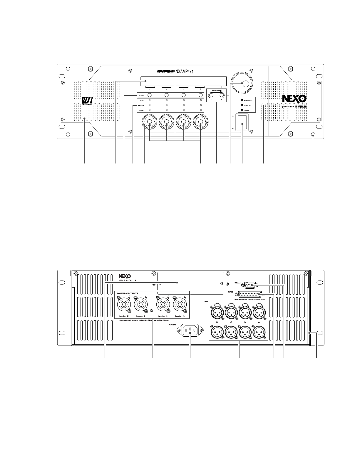
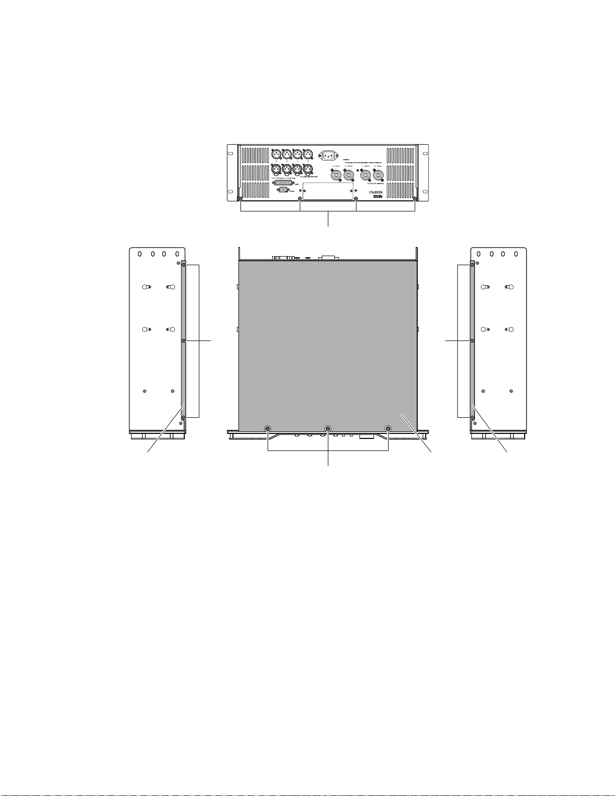
■ PANEL LAYOUT
A0 216 7 53 48 9
• Front Panel
NXAMP4x1
• Rear Panel
1 Power switch
2 Amplifier indicators
3 LCD display
4 Encoder
5 Navigation buttons (A & B)
6 Volume indicators
7 Mute buttons
8 Select buttons
9 Channel indicators
0 Air intakes
A Screw holes for handles
1 Mains connectors
2 Balanced audio inputs with link
3 Expansion slot
4 Power outputs
6 5 73 24 1
5 RS-232 Firmware update port
6 GPIO port
7 Rear end mounting holes
3
Page 4
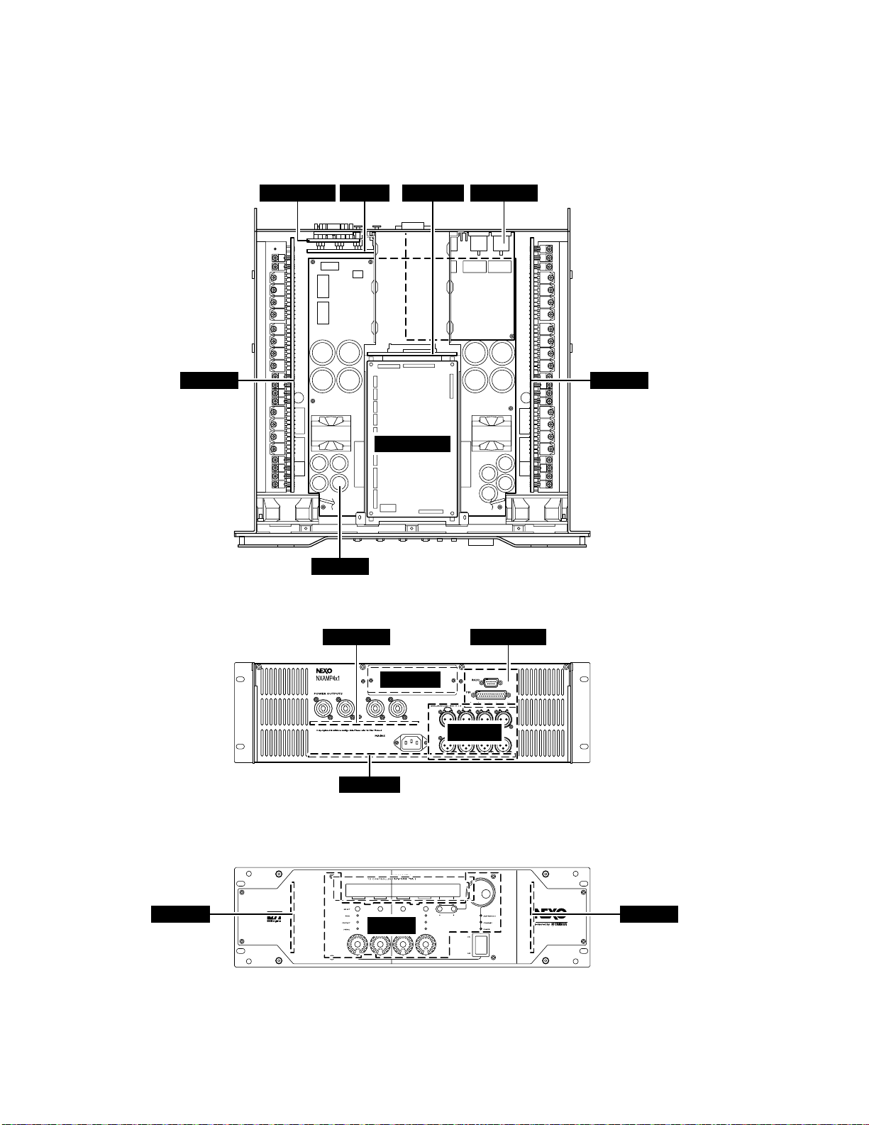
NXAMP4x1
■ CIRCUIT BOARD LAYOUT
PAANL
(PA unit)
RS232-GPI
PSANL
INANL
OPT-AN
CONTROL
OUTANL
PAANL
(PA unit)
Rear Panel
OUTANL
RS232-GPI
OPT-AN
INANL
PSANL
Front Panel
(PA unit) (PA unit)
PN-AN
PAANLPAANL
4
Page 5
C323 C322
C317 C316
C324 C318
C325
C205
C344 C354
C345 C355
C357
C356
C348
C347
C319
C323 C322
REAR
FRONT
C317 C316
C324 C318
C325
C205
C201C201
R213R213
C344 C354
C345 C355
C357
C356
C348
C347
C319
D305
220 ohms/
10W
220 ohms/
10W
220 ohms/
10W
220 ohms/
10W
220 ohms/10W220 ohms/10W
220 ohms/10W
220 ohms/10W220 ohms/10W
220 ohms/10W220 ohms/10W
220 ohms/10W
D306D306
1
3
4
2
CN316CN316
CN307 CN305CN307 CN305 CN308 CN309CN308
CN310CN310
CN309
6
7
5
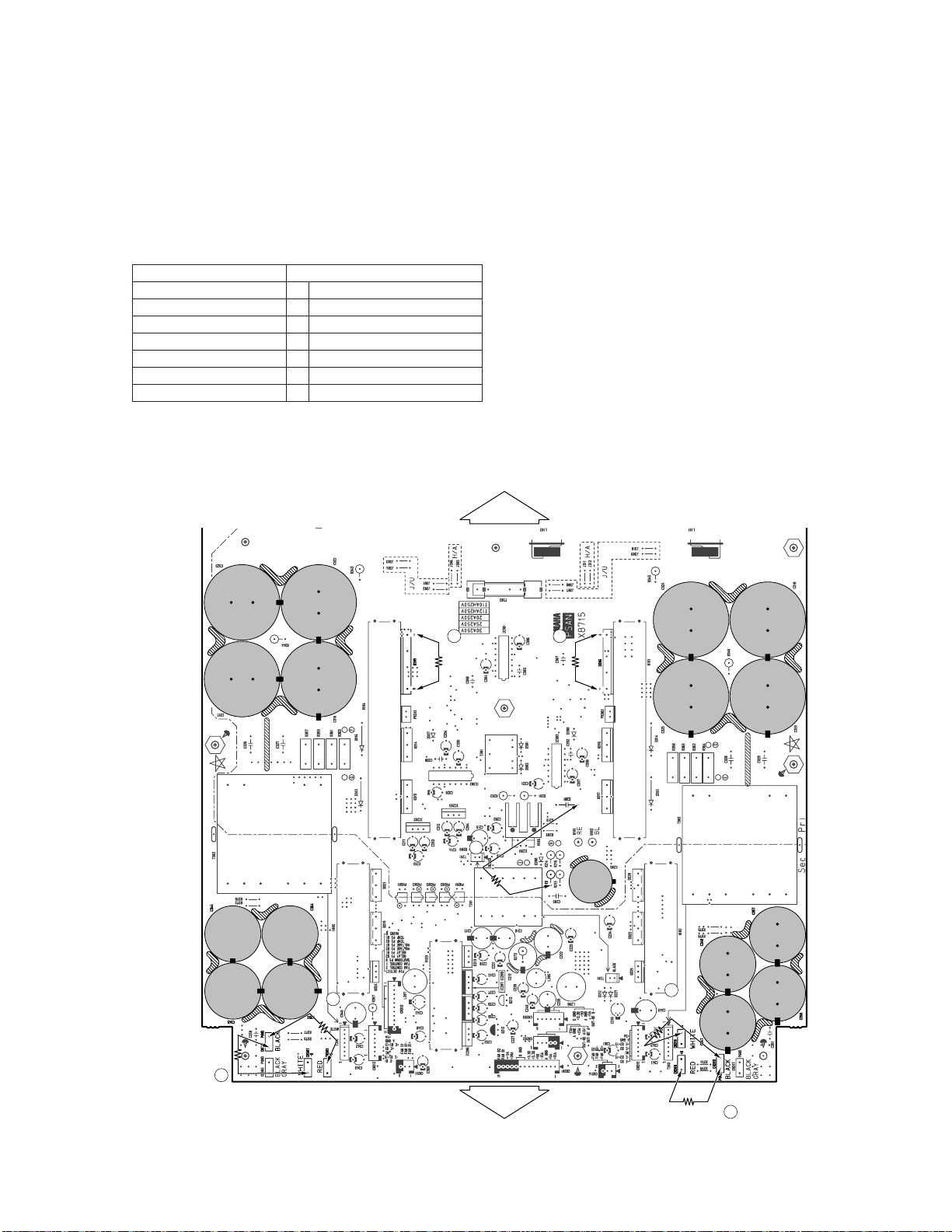
■ SERVICE PRECAUTIONS
Safety measures
• Some component parts on the PSANH circuit board maintain a high voltage even when the power is switched off.
For this reason to av oid an electrical shock, do not touch
the upper metallic part of the following capacitors until
the remaining voltage has discharged.
Capacitors Discharging point
C316, C317, C322, C323
C318, C319, C324, C325
C344, C354
C345, C355
C347, C356
C348, C357
C205
PSANL circuit board
1
D305: + pin <=> D305: - pin
2
D306: + pin <=> D306: - pin
3
CN305 <=> CN316
4
CN307 <=> CN316
5
CN308 <=> CN309
6
CN310 <=> CN309
7
R213: lead <=> C201
NXAMP4x1
[Discharging Method]
Before starting the service work, connect discharging
resistors (220 ohms 10W) to the terminals indicated in
the figure below to discharge electricity. (7 points)
The required discharging time is about 10 seconds. Check
that the DC voltage between the terminals measures close
to 0 (zero) volts using a multi-meter to mak e sure that the
discharge is completed.
Note:
Do not touch the IC201 and its heat sink before discharging the C205.
5
Page 6
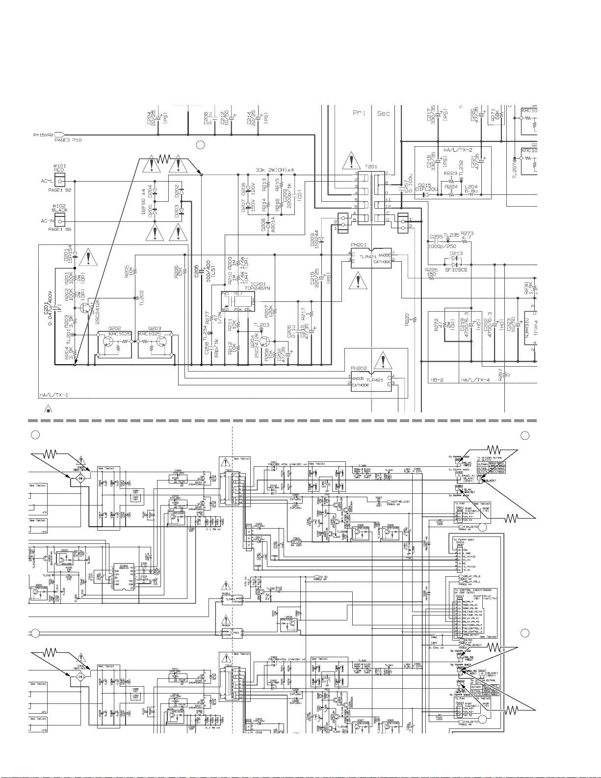
NXAMP4x1
C205
C201
C316
D305
C354C344
C355C345
C356C347
C357C348
C318
C319
D306
C305
C307
C316
220 ohms/10W
220 ohms/10W
PSANL circuit diagram
C201
220 ohms/10W
7
C205
1
220 ohms/10W
2
220 ohms/10W
6
D305
D306
C316
C322
C317 C323
C318
C324
C319 C325
220 ohms/10W
3
C305
C354C344
C316
C355C345
C307
4
220 ohms/10W
220 ohms/10W
5
C356C347
C357C348
6
220 ohms/10W
Page 7
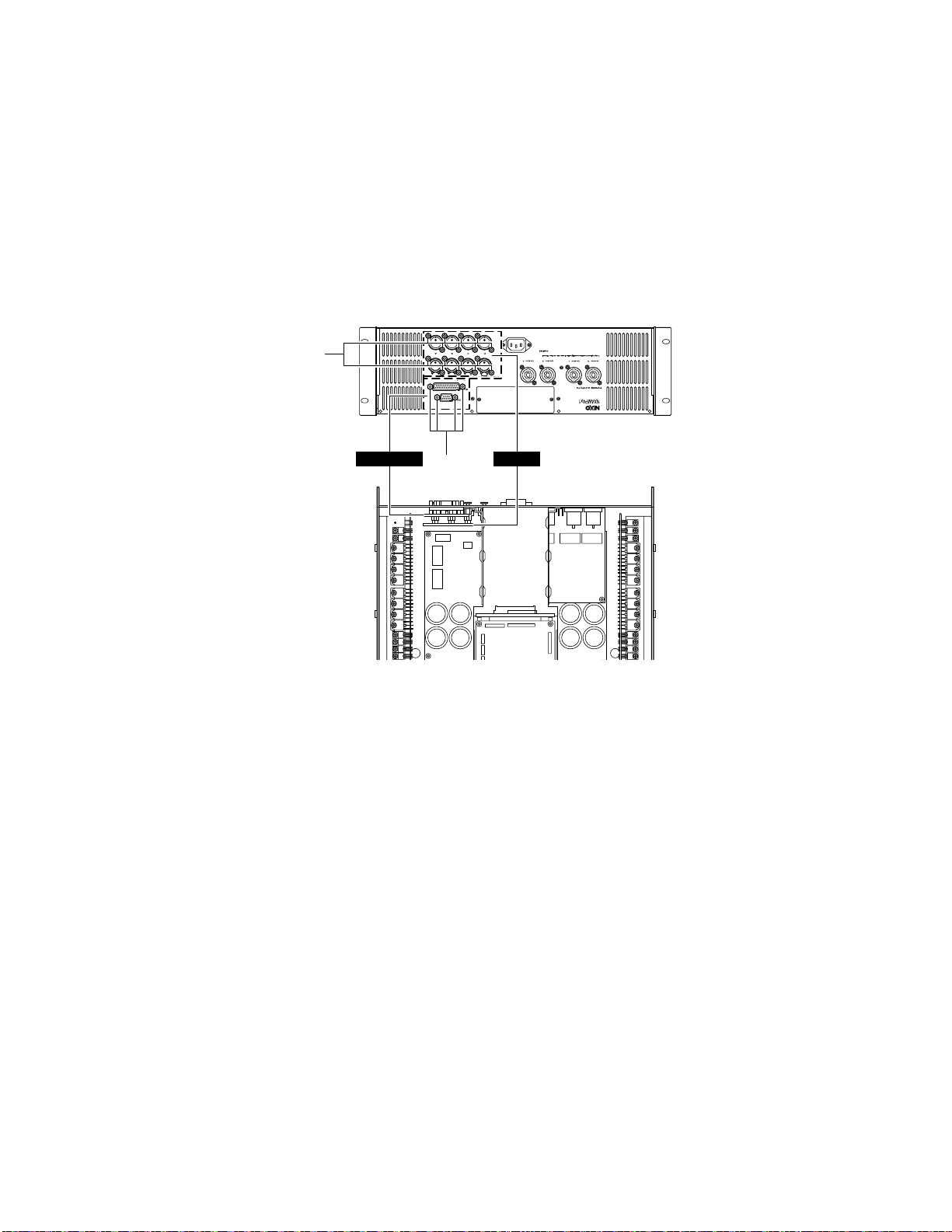
■ OVERALL ASSEMBLY WIRING
115 ± 1 mm
25 ± 1 mm
90˚
90˚
This product has various cables (wires and connector assemblies) inside. To prevent touching component to the cables and/
or connection mistake, perform the cable connection and fixing cables according to the following instructions referring the
wiring diagram, P3 of the circuit diagram.
Notice: Since the following pictures are taken of the preproduction product, they may differ from the commodity products in
detail. However, the wiring and so on is not so differ between them. So, refer only to wiring and so on.
1. Wiring of the PN-AN circuit board
1) Process the flat cable (WK02100). (Fig. 1)
2) Connect the flat cable (WK02100) to the PN-AN circuit board. (Fig. 2)
3) Install the PN-AN circuit board to the front panel. (Fig. 3)
NXAMP4x1
115 ± 1 mm
90˚
Fig. 1
Fig. 2 Fig. 3
90˚
25 ± 1 mm
2. Wiring of the power switch
1) Install the power switch to the front panel with its terminals set downward. (Fig. 4, 5)
Fig. 4 Fig. 5
7
Page 8
NXAMP4x1
Check
2) Confirm that the power switch is set to the off position as shown in the figure 6. (Fig. 6)
3) Twist the wires of the power switch assembly more than three times.
4) Connect the connector of the power switch assembly to the connector (CN103). (Fig. 7)
Check
Fig. 6
3. Wiring of the FAN
Connect the connector of the FAN to the each ter minal. (Fig. 8)
4. Attaching of the support cushion
Attach the support cushion (WN15950) at the specified
area on the pattern side of the CONTROL circuit board.
(Fig. 9)
Note: Be sure to remove the oil and the dust, etc. on the
attaching surface before attaching the support
cushion.
Fig. 7
Fig. 8
Fig. 9
8
Page 9
5. Wiring of the AC-INLET
Cord holder
Cord holder
a) Set a cord holder before installing the PSAN circuit board
on the enclosure. (Fig. 10)
NXAMP4x1
b) Set a ferrite-core at the specified area on the PSAN cir-
cuit board, and fasten the ferrite-core with the cord holder .
(Fig. 11)
Fig. 10
Fig. 11
c) Pass the live and neutral wires of the AC-INLET through the ferrite core’s hole twice and wind them to the ferrite core.
Screw an each screw terminal to the specified terminal. (Fig. 12, 13)
Fasten the GND wire with a cord holder. (U destination) (Fig. 12)
Screwing torque: GND LINE 1.8N • m / L, N LINE 0.78 • m
Cord holder
Cord holder
Fig. 12 Fig. 13
(U.S.A. model) (Chinese model)
d, e)Fix the wires to the terminal using the screws, and refer to the fig. 14 and fig. 15 for the direction of each terminal.
Fig. 14 Fig. 15
9
Page 10
NXAMP4x1
6. Wiring of the PA-UNIT
Connect the wires to the connectors (CN401, CN403). (Fig. 16, 17)
CN403
BLUE
CN401
RED
CN403
GREEN
Fig. 16 Fig. 17
NOTE: The followings are wires to be connected.
CN401: WK02080
CN403: WK90770
Install this PA-UNIT on the left side of enclosure.
Hereafter, this unit is called PA-UNIT of CH1,
CH2.
The following figure describes a layout drawing of the PA-UNITs seen from the front panel. (Fig. 18)
*
NOTE: The followings are wires to be connected.
CN401: WK90790
CN403: WK17110
Install this PA-UNIT on the right side of enclosure.
Hereafter, this unit is called PA-UNIT of CH3,
CH4.
CN401
YELLOW
CH2
BLUE
CH1
RED
PSANHL
CH3
YELLOW
CH4
GREEN
Fig. 18
7. Wiring of the flat cable and fastening wires
Connect the following wires at first.
CN313: WK68760
CN201: WK68770
a) Install the RS232-GPI circuit board on the enclosure after connecting the wire (WM15830) to it.
b) Connect the wires (WK16830, WN52530) from each PA UNIT to the FASTON terminals of the OUTANL circuit board.
PA-UNIT (CH1, CH2) : WN52530 (ORANGE) –> CN805
WK16830 (YELLOW) –> CN806
PA-UNIT (CH3, CH4) : WN52530 (ORANGE) –> CN807
WK16830 (YELLOW) –> CN808
Then fold the wires (WK16830, WF44430) at the center of them, and fasten them with a cord holder. (Fig. 19)
c) Connect the wires (WK16820 x2) to the connectors (CN306, CN317) of the PSAN circuit board.
Connect the wire (WK14200) to the connector (CN202) of the PSAN circuit board.
Fasten these wires with a cord holder at the position as shown in the figure. (Fig. 19)
d) Connect the wire (WK14210) of PA-UNIT (CH3, CH4) to the connector (CN315).
Fasten the wire (WK14210) and the wires (WK16820 x2, WK14200) with a cord holder at the position where the wire (WK14210)
is vertically pulled from PA-UNIT. Before fastening, pull the wires (WK16820 x2, WK14200) toward the front panel side in
advance.
10
Page 11
NXAMP4x1
a)
c)
b)
b)
e) d)
f)
f)
e) Connect the wire (WK14210) of PA-UNIT (CH1, CH2) to the connector (CN312).
Fasten the wire (WK14210) and the wire (WK02090) with a cord holder at the position where the wire (WK14210) is vertically
pulled from PA-UNIT. Before fastening, pull the wire (WK02090) toward the front panel side in advance.
f) Twist the wires (white, red and blac k) of PA-UNIT more than two times, and connect them to the FASTON terminals according
to the wire color displayed on the PSANL circuit board.
Then bend these wires, and fasten them with a cord holder. (Fig. 20)
a)
b)
c)
b)
e)
f)
d)
f)
Fig. 19
Fig. 20
11
Page 12
NXAMP4x1
g)
h)
g) Fasten these wires (WK17900, WK17910 and WK94710) with a cord holder to the hexagonal spacer. (Fig. 21)
h) Bend the wire (WK14200) and wire (WK16820) connected to the connector (CN317), and fasten the wires (WK14210, WK16820
x 2 and WK14200) with a cord holder. (Fig. 21)
h)
g)
Fig. 21
Note: When connecting the connector assembly to the CONTROL circuit board, confirm that the connector housing pin
number of the connector assembly is the same as the connector pin number of the circuit board.
i) Fasten the wires (WK02080, WK90770) with a cord holder at the hole of the RS232-GPI circuit board. (Fig. 22)
j) Fasten the wires (WK02080, WK90770 and WK02070) with a cord holder at the hole of the enclosure.
Fasten the wires (WK90790, WK17110) with a cord holder at the hole of the enclosure. (Fig. 22)
k) Fasten the wires (WK90790, WK17110) with a cord holder at the hole of the OPT-AN circuit board. Then connect the flat cable
(WK02120). (Fig. 22)
l) Fasten the wires (WK02080, WK90770, WK90790, WK17110 and WK02070) with a cord holder at the position close to the
OPT-AN circuit board. (Fig. 22)
m) Bend the wire (WK02090), and fasten the wires (WK02090, WK68760 and WK68770) with a cord holder. (Fig. 22).
n) Bend the flat cable as shown in the figure. (Fig. 22)
12
Page 13
i)
j)
*
1
j)
*
2
j)
*
2
j)
*
1
m)
o)
n)
l)
k)
k)
k)
The hole of the enclosure
NXAMP4x1
The hole of the enclosure
i)
j)
1
*
1
j)
*
n)
j)
2
*
j)
2
*
m)
o)
k)
k)
l)
Fig. 22
k)
13
Page 14
NXAMP4x1
Switch knob Switch knob
o) Bend the flat cable to avoid touching the top cover. (Fig. 23, 24)
Fig. 23 Fig. 24
8. Color of the connectors connected to the connector CN012-CN015
Connect the connector assembly from the PA unit to the CONTROL circuit board as shown in the figure below. (Fig. 25)
CN012
RED
CN013
BLUE
CN014
YELLOW
CN015
GREEN
Fig. 25
9. Change of the destination
Set the knob position of the switch SW001 on the CONTROL circuit board as shown in the figure below. (Fig. 26, 27)
U destination CHN destination
Switch knob Switch knob
14
Fig. 26 Fig. 27
Page 15
10. Insulation distance between WK17110 and primary side capacitor
Perform wiring the connector assembly WK17110 with care so that its uncovered portion with the SUMI tube does not touch
the capacitor C316 on primary side of the PSANL circuit board. (Fig. 28, 29)
Fig. 28 Fig. 29
NXAMP4x1
11. Insulation distance between WK14210 and primary side capacitor
Perform wiring the connector assembly WK14210 with care so that its uncovered portion with the SUMI tube does not touch
the capacitors C317 and C319 on primary side of the PSANL circuit board. (Fig. 30, 31)
C324 C318
C325 C319
Fig. 30
C323 C322
C317 C316
C324 C318
C325 C319
C323 C322
C317 C316
Fig. 31
15
Page 16
NXAMP4x1
12. Prevention of touching WK02070 to connector terminal
Perform wiring the connector assembly WK02070 with care so that its uncovered portion with the SUMI tube does not touch
the bare terminal of the connector CN203 of the RS232-GPI circuit board. (Fig. 32)
GPI circuit board
IOAN circuit board
Fig. 32
GPI circuit board
IOAN circuit board
13. Adhesive cloth tape
Cover the two scre ws near R587 and R588 in each PA unit (190 and 230) with adhesive cloth tape (185 and 225) as shown in
the figure below. (Fig. 33)
16
Fig. 33
Page 17
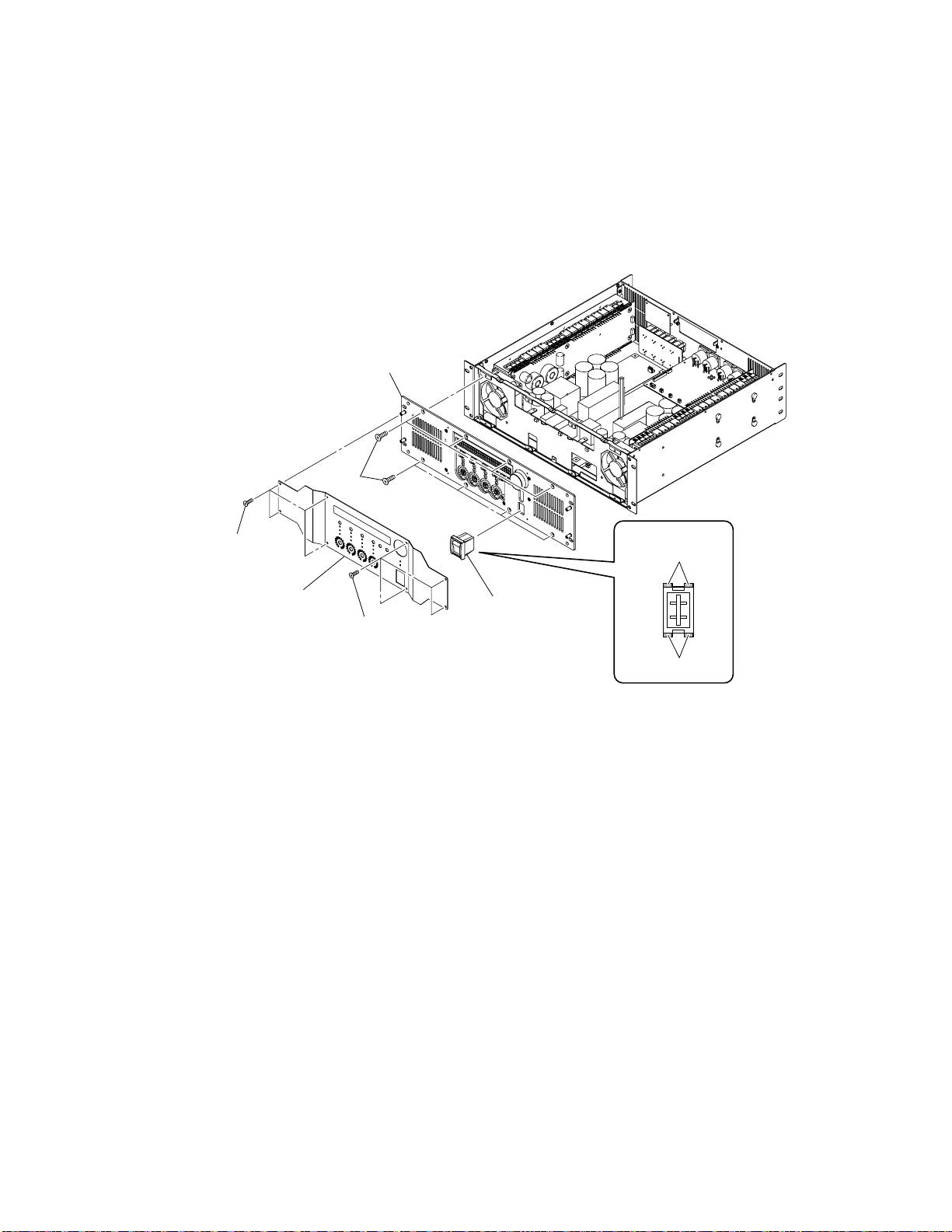
■ DISASSEMBLY PROCEDURES
1. Top Cover (Time required: about 3 minutes)
1-1. Remove the thirteen (13) screws marked [650]. (Fig. 1)
1-2. The top cover can then be removed. (Fig. 1)
NXAMP4x1
[650]
[650] [650]
[650]: Bind Head Screw 4x8 MFZN2B3 (--)
(Fig. 1)
Top cover Top coverTop cover
[650]
17
Page 18
NXAMP4x1
2. CONTROL Circuit Board, OPT angle and OPT-AN Circuit Board
(Time required: about 10 minutes)
2-1. Remove the top cover. (See procedure 1.)
2-2. Remove the four (4) screws marked [430]. (Fig. 2)
2-3. Disconnect the connector assemblies from other units connected to the CONTROL circuit board. (Fig. 2)
2-4. The CONTROL circuit board can then be removed. (Fig. 2)
2-5. Remove the three (3) screws marked [400] and the two (2) screws marked [410]. (Fig. 2)
2-6. Remove the OPT angle with the OPT-AN circuit board. (Fig. 2)
2-7. Remove the two (2) screws marked [380]. (Fig. 2)
2-8. The OPT-AN circuit board can then be removed. (Fig. 2)
OPT-AN
OPT angle
[380]: Bind Head Tapping Screw-S 3x6 MFZN2W3 (--)
[400]: Bind Head Tapping Screw-S 3x6 MFZN2W3 (--)
[410]: Bind Head Tapping Screw-S 3x6 MFZN2B3 (--)
[430]: Bind Head Tapping Screw-S 3x6 MFZN2W3 (--)
[380]
[410]
OPT angle
OPT-AN
[430]
[400]
CONTROL
[430][400] [400]
18
(Fig. 2)
Page 19
NXAMP4x1
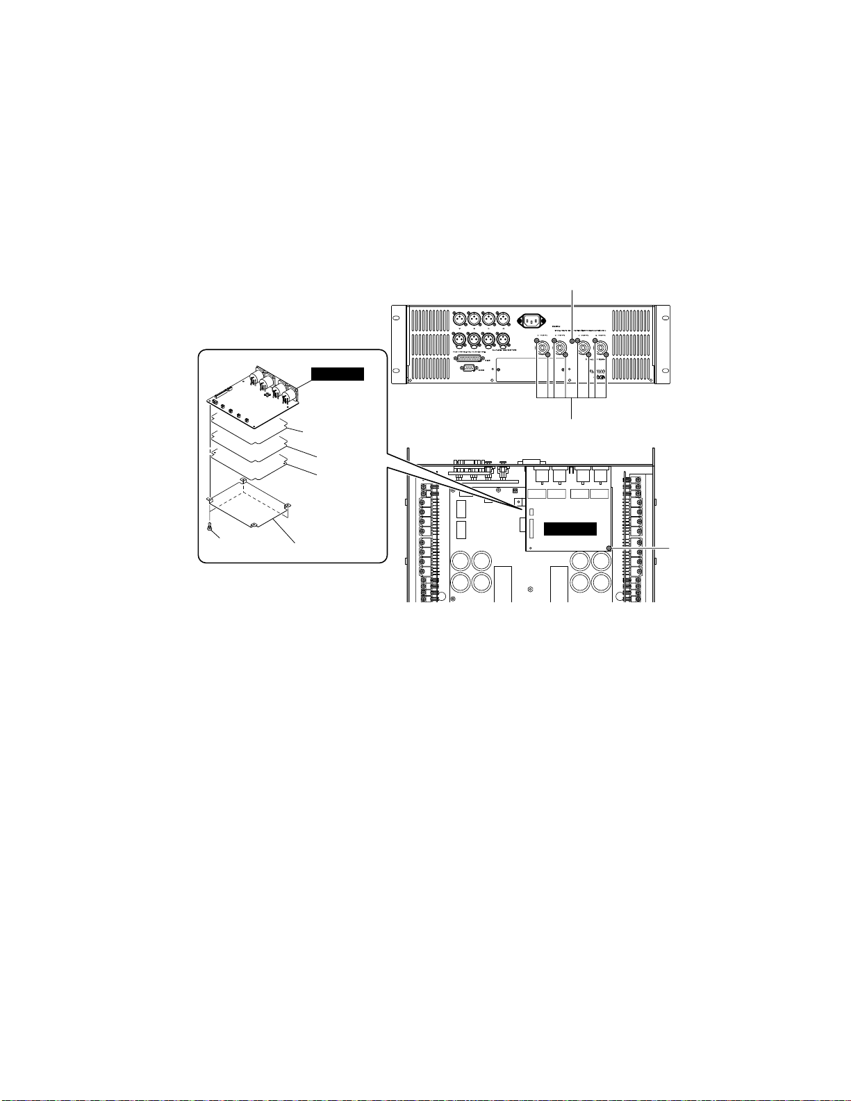
3. OUTANL Circuit Board (Time required: about 15 minutes)
3-1. Remove the top cover. (See procedure 1.)
3-2. Remove the CONTROL circuit board and the OPT angle. (See procedure 2.)
3-3. Remove the eight (8) screws marked [280], the one (1) screw marked [290] and the one (1) screw marked [285]. (Fig. 3)
3-4. Disconnect the connector assemblies from other units connected to the OUTANL circuit board. (Fig. 3)
3-5. The OUTANL circuit board with the two (2) insulation sheets and the two (2) shields can then be removed. (Fig. 3)
3-6. Remove the three (3) plastic rivets marked [277]. (Fig. 3)
3-7. Remove the insulation sheet 1, the shield 1, the shield 2 and the insulation sheet 2 from the OUTANL circuit board. (Fig. 3)
[290]
OUTANL
Insulation
sheet 2
Shield 2
Shield 1
[277]
[277]: Plastic Rivet NRP-345 (--)
[280]: Flat Head Tapping Screw-B 3x8 MFZN2B3 (--)
[285]: Bind Head Tapping Screw-S 3x6 MFZN2W3 (--)
[290]: Bind Head Tapping Screw-B 3x8 MFZN2B3 (--)
Insulation sheet 1
(Fig. 3)
[280]
OUTANL
[285]
19
Page 20
NXAMP4x1
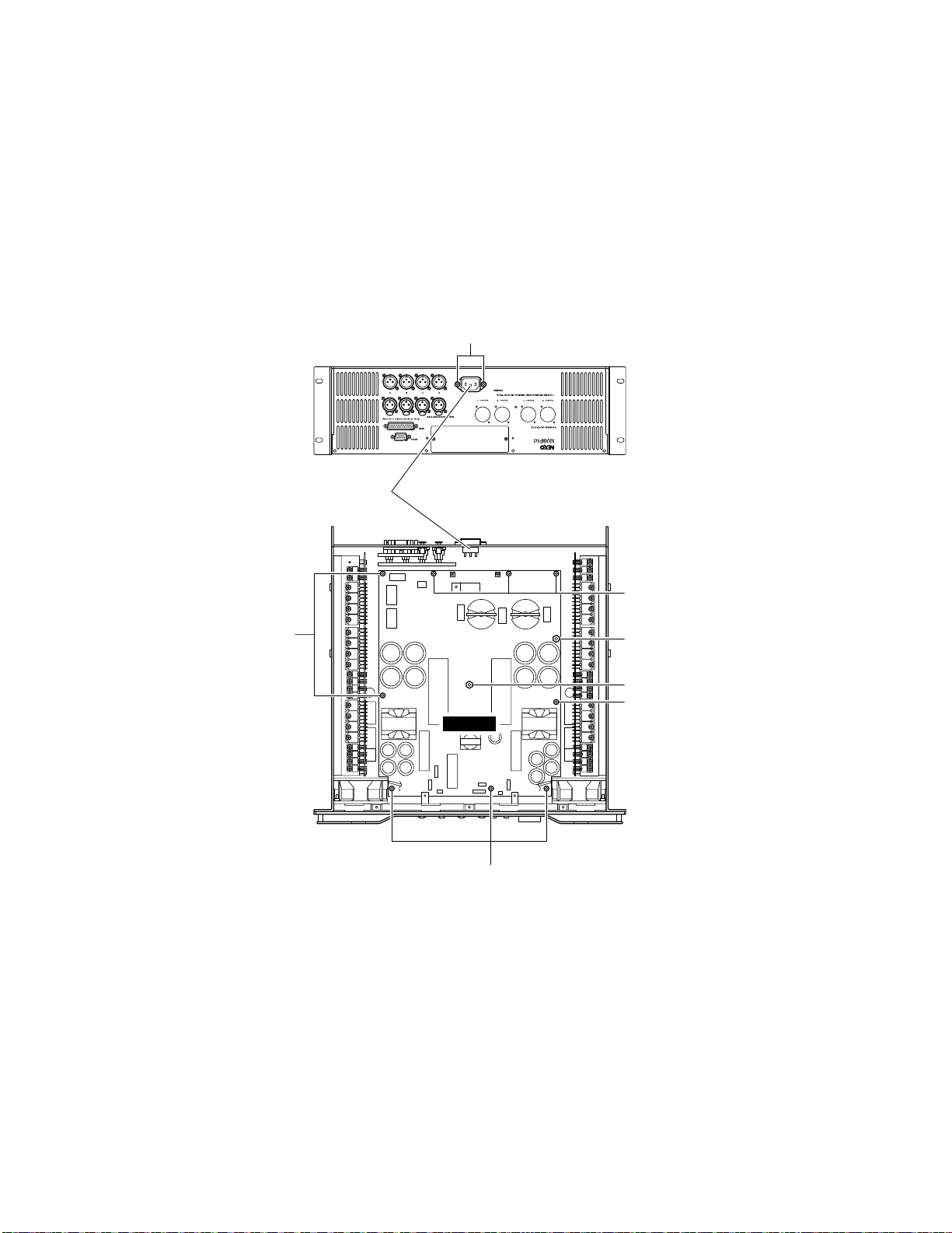
4. PSANL Circuit Board (Time required: about 20 minutes)
4-1. Remove the top cover. (See procedure 1.)
4-2. Remove the CONTROL circuit Board and the OPT angle. (See procedure 2.)
4-3. Remove the OUTANL Circuit Board. (See procedure 3.)
4-5. Remove the two (2) screws marked [150], and remove the ACPS connector assembly. (Fig. 4)
4-6. Remove the nine (9) screws marked [100], the one (1) hexagonal spacers marked [90] and the one (1) hexagonal spacer
marked [95]. (Fig. 4)
4-7. Disconnect the connector assemblies from other units connected to the PSANL circuit board. (Fig. 4)
4-8. The PSANL circuit board can then be removed. (Fig. 4)
[150]
ACPS connector assembly
[100]
PSANL
[100]
[90]: Hexagonal Spacer H=89 B=5.5 (--)
[95]: Hexagonal Spacer H=41 B=5.5 (--)
[100]: Bind Head Tapping Screw-S 3x6 MFZN2W3 (--)
[150]: Flat Head Tapping Screw-B 3x8 MFZN2B3 (--) (U destination)
[150]: Bind Head Tapping Screw-B 3x8 MFZN2B3 (--) (O destination)
[100]
[95]
[90]
[100]
20
(Fig. 4)
Page 21
NXAMP4x1
5. INANL Circuit Board (Time required: about 7 minutes)
5-1. Remove the top cover. (See procedure 1.)
5-2. Remove the sixteen (16) screws marked [70]. (Fig. 5)
5-3. Disconnect the connector assembly from other unit con-
nected to the INANL circuit board. (Fig. 5)
5-4. The INANL circuit board can then be removed. (Fig. 5)
[70]
RS232-GPI
[330]
6. RS232-GPI Circuit Board (Time required: about 7 minutes)
6-1. Remove the top cover. (See procedure 1.)
6-2. Remove the four (4) hexagonal lock screws marked
[330]. (Fig. 5)
6-3. Disconnect the flat cable from other unit connected to
the RS232-GPI circuit board. (Fig. 5)
6-4. The RS232-GPI circuit board can then be removed.
(Fig. 5)
INANL
[70]: Bind Head Tapping Screw-B 2.6x8 MFZN2B3 (--)
[330]: Hexagonal Lock Screw (--)
(Fig. 5)
21
Page 22
NXAMP4x1
7. Left (CH1, CH2) PA unit (Time required: about 15 minutes)
7-1. Remove the top cover. (See procedure 1.)
7-2. Remove the CONTROL circuit board and the OPT
angle. (See procedure 2.)
7-3. Remove the four (4) screws marked [670A], and re-
move the four (4) screw covers marked [660A]. (Fig. 6)
7-4. Remove the six (6) screws marked [220]. (Fig. 6)
7-5. Disconnect the connector assemblies that connects the
left PA unit and other units. (Fig. 6)
7-6. The left PA unit can then be removed. (Fig. 6)
[220]
[660A]
PA unit
[670A]
[660A]
8. Right (CH3, CH4) PA unit (Time required: about 15 minutes)
8-1. Remove the top cover. (See procedure 1.)
8-2. Remove the CONTROL circuit board and the OPT
angle. (See procedure 2.)
8-3. Remove the four (4) screws marked [670B], and re-
move the four (4) screw covers marked [660B]. (Fig. 6)
8-4. Remove the six (6) screws marked [260]. (Fig. 6)
8-5. Disconnect the connector assemblies that connects the
right PA unit and other units. (Fig. 6)
8-6. The right PA unit can then be removed. (Fig. 6)
PA unit
[220]
[220]: Bind Head Screw 4x8 MFZN2B3 (--)
[260]: Bind Head Screw 4x8 MFZN2B3 (--)
[660A]: Screw Cover T5N (--)
[660B]: Screw Cover T5N (--)
[670A]: Bind Head Tapping Screw-B 3x8 MFZN2B3 (--)
[670B]: Bind Head Tapping Screw-B 3x8 MFZN2B3 (--)
(Fig. 6)
[660B]
[670B]
[660B]
[260]
22
Page 23
NXAMP4x1
[500]
[500]
[40]
[510]
[590]
[590]
Front panel assembly
Front panel 2
Power switch
Power switch
HookHookHook
Hook
LCD assembly
LCD assembly
LCD unit
PN-AN
[40]
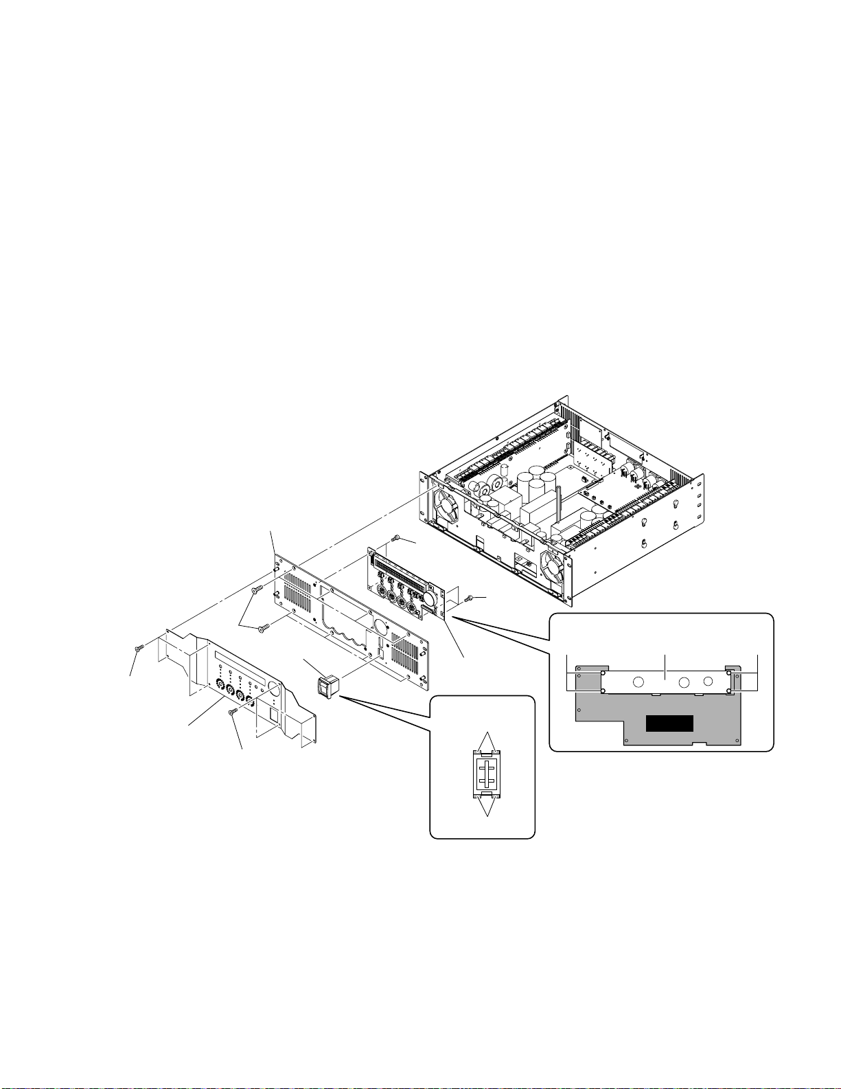
9. Front Panel Assembly
(Time required: about 6 minutes)
9-1. Remove the top cover. (See procedure 1.)
9-2. Remove the CONTROL circuit Board and the OPT
angle. (See procedure 2.)
9-3. Remove the eight (8) screws marked [590]. (Fig. 7)
9-4. Remove the front panel 2. (Fig. 7)
9-5. Disconnect the connector of the power switch assem-
bly connected to the PSANL circuit board. (Fig. 7)
9-6. Remove the eight (8) screws marked [510]. (Fig. 7)
9-7. Disconnect the flat cable from other unit connected to
the PN-AN circuit board. (Fig. 7)
9-8. The front panel assembly can the be removed. (Fig. 7)
10. PN-AN Circuit Board (Time required: about 10 minutes)
10-1. Remove the top cover. (See procedure 1.)
10-2. Remove the front panel assembly. (See procedure 9.)
10-3. Remove the five (5) screws marked [500]. (Fig. 7)
10-4. Remove the LCD assembly. (Fig. 7)
10-5. Remove the four (4) nylon rivets [40]. (Fig. 7)
10-6. The PN-AN circuit board and the LCD unit can then be
separated. (Fig. 7)
[40]: Nylon Rivet (--)
[500]: Bind Head Screw 3x4 MFZN2B3 (--)
[510]: Flat Head Screw 4x8 MFZN2B3 (--)
[590]: Bind Head Tapping Screw-S 3x6 MFZN2B3 (--)
(Fig. 7)
23
Page 24
NXAMP4x1
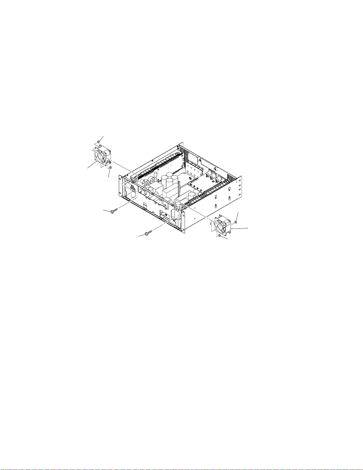
11. Left DC Fan (Time required: about 15 minutes)
11-1. Remove the top cover. (See procedure 1.)
11-2. Remove the CONTROL circuit board and the OPT
angle. (See procedure 2.)
11-3. Remove the front panel assembly. (See procedure 9.)
11-4. Remove the two (2) screws marked [40A] and the two
(2) hexagonal nuts marked [50A]. (Fig. 8)
11-5. Disconnect the connector of the left DC fan connected
to the PSANL circuit board. (Fig. 8)
11-6. The left DC fan can then be removed. (Fig. 8)
[50A]
DC fan
[50A]
[40A]
12. Right DC fan (Time required: about 15 min utes)
12-1. Remove the top cover. (See procedure 1.)
12-2. Remove the CONTROL circuit board and the OPT
angle. (See procedure 2.)
12-3. Remove the front panel assembly. (See procedure 9.)
12-4. Remove the two (2) screws marked [40B] and the two
(2) hexagonal nuts marked [50B]. (Fig. 8)
12-5. Disconnect the connector of the right DC fan connected
to the PSANL circuit board. (Fig. 8)
12-6. The right DC fan can then be removed. (Fig. 8)
[50B]
[40B]
[40A]: Bind Head Screw 4x35 MFZN2W3 SP (--)
[40B]: Bind Head Screw 4x35 MFZN2W3 SP (--)
[50A]: Hexagonal Nut M4 #1 (--)
[50B]: Hexagonal Nut M4 #1 (--)
(Fig. 8)
DC fan
[50B]
24
Page 25
NXAMP4x1
Hook
13. Power switch (Time required: about 15 minutes)
13-1. Remove the top cover. (See procedure 1.)
13-2. Remove the CONTROL circuit Board and the OPT angle. (See procedure 2.)
13-3. Disconnect the connector of the power switch assembly connected to the PSANL circuit board. (Fig. 9)
13-4. Remove the front panel assembly. (See procedure 9.)
13-5. Release the four (4) hooks of the power switch, and remove the power switch from the front panel assembly. (Fig. 9)
Front panel assembly
[510]
[590]
Front panel 2
[590]
[510]: Flat Head Screw 4x8 MFZN2B3 (--)
[590]: Bind Head Tapping Screw-S 3x6 MFZN2B3 (--)
Power switch
(Fig. 9)
Power switch
Hook
Hook
Hook
25
Page 26
NXAMP4x1
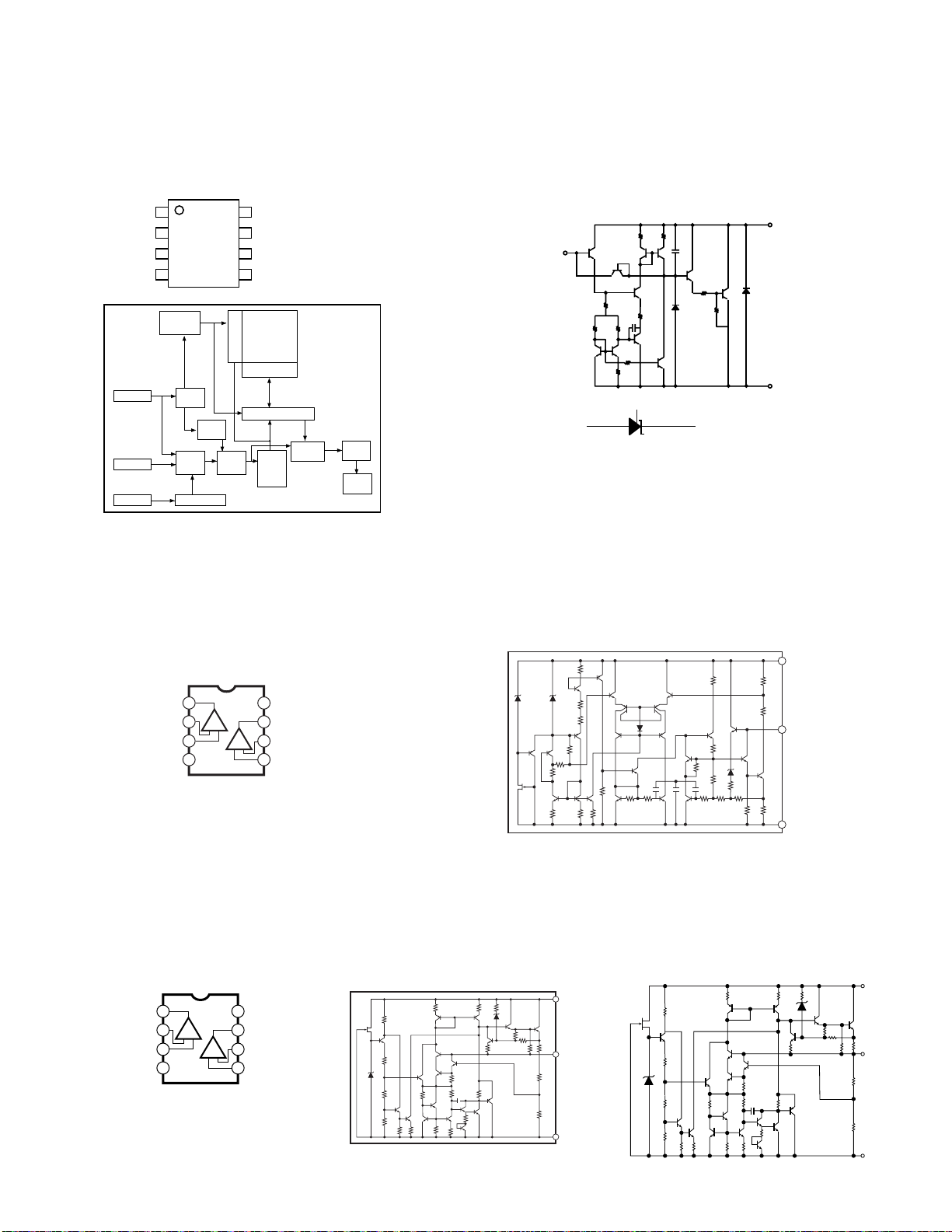
■ LSI PIN DESCRIPTION
• PCM1803ADBR (X7357B0) A/D CONVERTER CONTROL: IC035, IC036, IC037, IC038
PIN
NO.
10
11
12
13
14
15
16
17
18
19
20
(1) Schmitt trigger input
(2) Schmitt trigger input with internal pulldown (50 kΩ, typically), 5 V tolerant
(3) Schmitt trigger input, 5 V tolerant
NAME
1
2
3
4
5
6
7
8
9
VINL
V
INR
REF1
V
V
REF2
VCC
AGND
PDWN
BYPAS
TEST
LRCK
BCK
DOUT
DGND
V
DD
SCKI
OSR
FMT0
FMT1
MODE0
MODE1
I/O FUNCTION
I
Analog input, L-channel
Analog input, R-channel
I
–
Reference voltage 1 decoupling capacitor
–
Reference voltage 2 decoupling capacitor
Analog power supply, 5 V
–
–
Analog GND
I
Power-down control, active-low
I
HPF bypass control / LOW: Normal mode (dc reject); HIGH: Bypass mode (through)
I
Test, must be connected to DGND
I/O
Audio data latch enable input/output
I/O
Audio data bit clock input/output
O
Audio data digital output
–
Digital GND
–
Digital power supply, 3.3 V
I
System clock input: 256 fs, 384 fs, 512 fs or 768 fs
I
Oversampling ratio select input / LOW: x 64 fs, HIGH: x 128 fs
I
Audio data format select input 0 / See data format section
I
Audio data format select input 1 / See data format section
I
Mode select input 0 / See data format section
I
Mode select input 1 / See data format section
(2)
(2)
(1)
(1)
(3)
(2)
(2)
(2)
(2)
(2)
(2)
26
Page 27
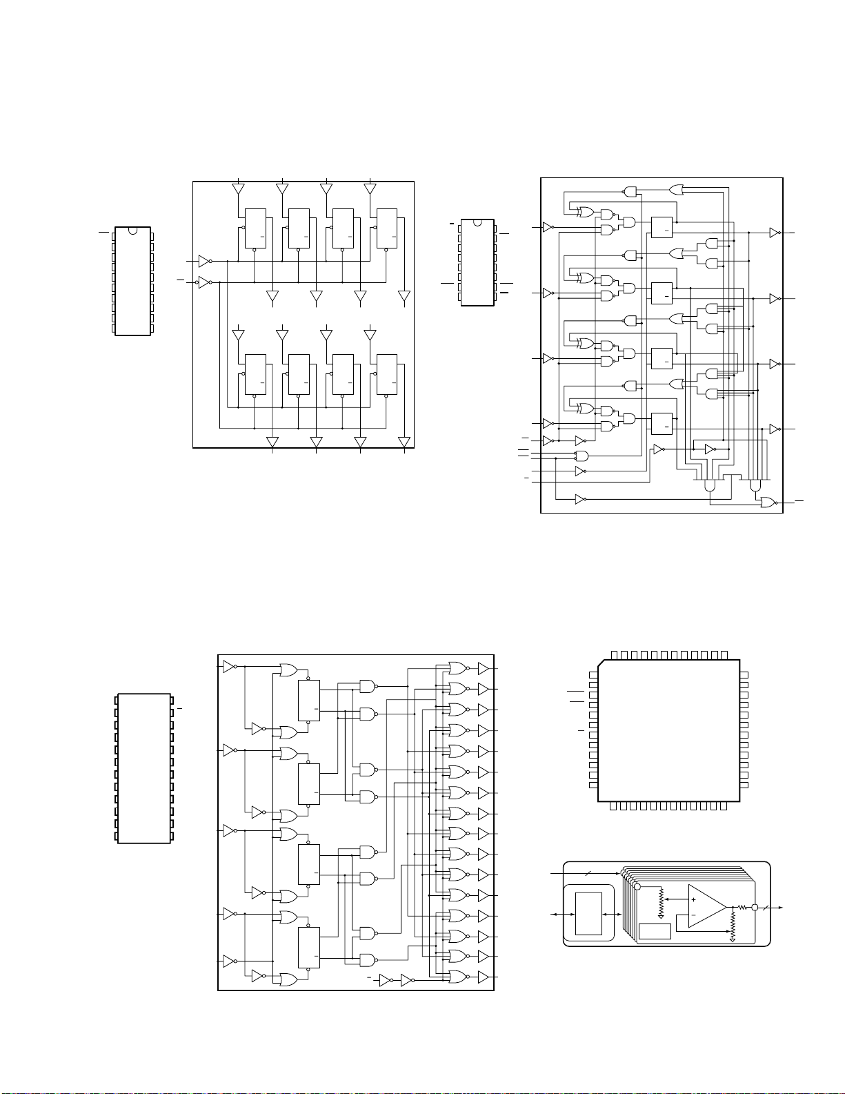
■ IC BLOCK DIAGRAM
NXAMP4x1
• 74HCT273PW,118 (X8681A0)
D-type Flip Flop
PN-AN: IC002, 003
D0
CP
MR
GND
1
20
V
2
Q0
3
D0
4
D1
5
Q1
6
Q2
7
D2
8
D3
9
Q3
10
CC
19
Q7
18
D7
CP
17
D6
16
Q6
MR
15
Q5
14
D5
13
D4
12
Q4
11
CP
FF1
R
D
D4
CP
FF5
R
D
• 74LVC169PW,118 (X8482A0)
Binaly Counter
CONTROL: IC044, 045
D1
QD
Q
Q0
D5
QD
Q
Q4
D2
QD
CP
FF2
Q
R
D
Q1
D6
QD
CP
FF6
Q
R
D
Q5
D3
QD
CP
FF3
Q
R
D
QD
CP
FF7
Q
R
D
QD
CP
FF4
Q
R
D
Q2
Q6
Q3
D7
QD
CP
FF8
Q
R
D
Q7
U/D
CEP
GND
1
16
CP
2
15
D0
3
14
D1
4
13
5
12
D2
6
11
D3
7
10
8
9
V
TC
Q0
Q1
Q2
Q3
CET
PE
3
DC
CC
4
D1
5
D2
6
D3
9
PE
7
CEP
10
CET
2
CP
1
U/D
Q
D
CP
Q
Q
D
CP
Q
Q
D
CP
Q
Q
D
CP
Q
14
Q0
13
Q1
12
Q2
11
Q3
15
TC
• 74HCT4514PW,118 (X8630A0)
Decoder
PN-AN: IC004-007
A
0
V
24
Q
Q
Q
Q
Q
Q
Q
Q
GND
1
LE
A
2
0
A
3
1
4
7
5
8
6
5
7
4
8
3
9
1
10
2
11
0
12
CC
23
E
A
22
3
21
A
2
20
19
18
17
16
15
14
13
A
Q
1
10
Q
11
Q
8
Q
9
Q
14
Q
15
Q
A
12
2
Q
13
A
3
LE
latch
latch
latch
latch
• CS3318-CQZ (X8486A0)
Volume Controller
CONTROL: IC001
REFO1
OUT1
OUT2
REFO2
IN2
VA-
VA+
Q
0
S
D
Q
1
Q
R
D
S
D
Q
2
Q
R
D
S
D
Q
3
Q
R
D
S
D
Q
4
Q
R
D
E
Q
1
Q
2
Q
3
Q
4
Q
5
Q
6
Q
7
Q
8
Q
9
Q
10
Q
11
Q
12
Q
13
Q
14
Q
15
8-channel
Analog
Inputs
I2C/SPI
Serial
Control
REFI1
RESET
MUTE
SCL/CCLK
SDA/MOSI
AD0/CS
ENOut
DGND
REFI8
±8V to ±9V
+3.3V
4847464544434241403938
1
IN1
2
3
4
5
6
7
8
9
VD
10
11
IN8
12
1314151617181920212223
OUT8
REFO8
5
I2C/SPI
Control
Port
VA+
VA-
OUT7
Zero Crossing
Detector
REFO7
IN7
REFI2
REFI7
REFI3
REFI8
OUT3
REFO3
IN3
37
36
VA-
35
VA+
34
OUT5
33
REFO4
32
IN4
31
REFI4
30
REFI5
29
IN5
REFO5
28
OUT5
27
VA-
26
VA+
25
24
IN6
OUT6
REFO6
8-channel
3
Analog
Outputs
27
Page 28
NXAMP4x1
• CS4272-CZZR (X8487A0)
CODEC
CONTROL: IC012, 013
3.3V to 5V2.5V to 5V
Hardware or
I2C/SPI
Control Data
Reset
Serial
Audio
Intput
Serial
Audio
Output
Registor/Hardware
Level Translator Level Translator
Configuration
Volume
Control
Volume
Control
PCM Serial Interface/Loopback
• IR2110 (X2382A02)
Driver
PSANL: IC302, 303
Selectable
Interpolation
Filter
Mixer
Selectable
Interpolation
Filter
High Pass Filter and
DC Offset Calibration
High Pass Filter and
DC Offset Calibration
Internal Voltage
Reference
∆∑ Modulator
∆∑ Modulator
LOW-Latency
Anti-Alias Filter
LOW-Latency
Anti-Alias Filter
Internal
Oscilator
5V
External
Mute Control
Switched Capasito
DAC and Filterr
Switched Capasito
DAC and Filterr
Multibit
Oversampling
ADC
Multibit
Oversampling
ADC
Left and
Right Mute
Controls
Left
Differential
Output
Right
Differential
Output
Left
Differential
Input
Right
Differential
Input
• DSPB56371AF180 (X8489A0)
DSP
CONTROL: IC022, 023
5
SHI
Interface
2
EXTAL
RESET
PINIT/NMI
212
Triple
Timer
DAX
Address
Generation
Unit
Six Channel
DAM Unit
Bootstrap
ROM
Internal
Data
Bus
Switch
Clock
Gen-
erator
PLL
ESAI
Interface
12
ESAI_1
Interface
Program
Interruput
Controller
Expansion Area
PIO_EB
11
GPIO
Peripheral
Program
Decode
Controller
MODA/IRQA
MODB/IRQB
MODC/IRQC
MODD/IRQD
EFCOP
Program
Address
Controller
Program
RAM
4K x 24
ROM
64K x 24
YAB
PM_EB
XAB
PAB
DAB
24-Bit
DSP56300
Core
DDB
YDB
XDB
PDB
GDB
24 x 24+56 56-bit MAC
Two 56-bit Accumulators
Memory Expansion Area
X Data
RAM
36K x 24
ROM
32K x 24
XM_EB
Data ALU
56-it barrel Shifter
Y Data
RAM
48K x 24
ROM
32K x 24
YM_EB
Power
Mngmnt.
JTAG
OnCE
4
TM
COM
VCC
1
LO
2
3
4
5
VS
6
VB
HO
7
14
13
VSS
12
LIN
11
SD
10
HIN
9
VDD
8
• LD1117STR (X8495A0)
Regulator
CONTROL: IC024
VOLTAGE
GENERATOR
CURRENT
GENERATOR
V
B
HV
UV
9
V
DD
10
HIN
11
SD
LIN
12
V
SS
13
Q
R
S
S
Q
R
VDD/V
LEVEL
SHIFT
VDD/V
LEVEL
SHIFT
CC
PULSE
PULSE
GEN
GEN
CC
LEVEL
SHIFT
DETECT
PULSE
FILTER
UV
DETECT
DELAY
R
Q
R
S
6
7
HO
5
V
S
3
CC
V
LO
1
2
COM
• MAX3221CPWR (X2757A0)
RS-232C Driver
CONTROL: IC041
V
IN
C1+
C1–
C2+
C2–
RIN
EN
1
2
3
V+
4
5
6
7
V–
8
16
15
14
13
12
11
10
9
FORCEOFF
V
CC
GND
DOUT
FORCEON
DIN
INVALID
ROUT
DIN
11
13
DOUT
THERMAL
COMPENSATION
28
THERMAL
PROTECTION
FORCEOFF
V
OUT
GND
16
12
FORCEON
9 8
ROUT
Auto-powerdown
10
1
INVALID
RIN
EN
Page 29
NXAMP4x1
CATHOD
REFERENCE
ANODE
(A)
CATHODE
(K)
REFERENCE (R)
ANODE
CS#
SO
GND
VCC
HOLD#
1
2
3
4
5
6
7
8
SI
WP#
SCLK
Data
Register
SRAM
Buffer
Output
Buffer
Sense
Amplifire
HV
Generator
Mode
Logic
SO
State
Machine
SI
Y-Decoder
Memory Array
Page Buffer
X-Decoder
CS#
Address
Generator
SCLK
Clock Generator
1
2
3
4
-V
8
7
6
5
Output A
+V
Non-Inverting
Input A
-DC Voltage Supply
+DC Voltage
Supply
Output B
Inverting
Input B
Non-Inverting
Input B
Inverting
Input A
+-
+-
1
2
3
4-V
8
7
6
5
Output A
+V
Non-Inverting
Input A
Ground
+DC Voltage
Supply
Output B
Inverting
Input B
Non-Inverting
Input B
Inverting
Input A
+-
+-
COMMON
OUTPUT
R23
R24
R13
R14
R20
R17
D3
Q22
Q21
Q25
Q20
Q24
Q18
Q9
R18
R19
R16R15R21R12R11
R10
Q17
R9R8
R7
R5
R4
D2D1
R6
C1 C2
C3
R22
Q11
Q13
Q14
Q15
Q19
Q16
Q23
Q8
Q7
Q2
Q1
Q6
Q5
Q3
Q10
Q12
Q4
R1
R2
R3
INPUT
INPUT
OUTPUT
GND
INPUT
OUTPUT
GND
• MX25L1605AM2C-12G (X8718A0)
Flash Memory
CONTROL: IC039
• NJM431U (TE1) (X6770A0)
SHUNT Regulator
PSANL: IC204
• NJM2068M-D (X3505A0)
Operational Amplifier
CONTROL: IC002-005, 008-011, 018-021, 028-034
INANL: IC701, 702
OUTANL: IC801, 802
• NJM79M09DL1A (X5366A0)
Regulator
CONTROL: IC007
• NJM7815FA (XD853A0)
Regulator +15V
PSANL: IC202, 203
• NJM78M09DL1A (XZ940A0)
Regulator
CONTROL: IC006
• NJM2904V (TE1) (XR532A0)
Operational Amplifier
CONTROL: IC047, 048, 050, 052
29
Page 30
NXAMP4x1
• NJU7630-M (X8682A0)
Regulator
PSANL: IC205
V+
1V
Vref
Soft Start
2
ER.AMP
UVLO
Latch
2µA
SCP
2kΩ
0.5
R
1V
1V
FB
IN-
SCP
3
4
5
PWM
OSC
0.5V
67 8
RT
GND
R
T
DTC
A
T
0.8V
0.2V
Buffer
• PCM1803ADBR (X7357B0)
A/D Converter
CONTROL: IC035-038
Delta-Sigma
Modulator
Delta-Sigma
Modulator
DGND
20
MODE1
19
MODE0
18
FMT1
17
FMT0
16
OSR
15
SCKI
14
V
DD
13
DGND
12
DOUT
11
BCK
BCK
LRCK
x 1/64, x 1/128
Decimation
Filter
With
High-Pass Filter
Clock and Timing Control
V
DD
Serial
Interface
Mode/
Format
Control
DOUT
FMT0
FMT1
MODE0
MODE1
BYPAS
TEST
OSR
PDWN
SCKI
1
VINL
2
R
V
IN
3
V
1
REF
4
2
V
REF
5
V
CC
6
AGND
7
PDWN
TEST
LRCK
Reference
CC
8
9
10
Power Supply
AGNDV
BYPAS
V
L
OUT
1
IN
1
V
REF
V
2
REF
V
R
IN
• PQ1CX12H2ZP (X6188A0)
Regulator
PSANL: IC208
1 8
V
IN
Drive
2
V
B
Circuit
Comparator
Over
current
Detection
circuit
Over
Heat
Detection
circuit
Q
R
F/F
S
6, 7
COM
Oscill
ator
fo Conversion
circuit
Voltage
regulator
ON/OFF
circuit
+
-
AMP
Soft
Start
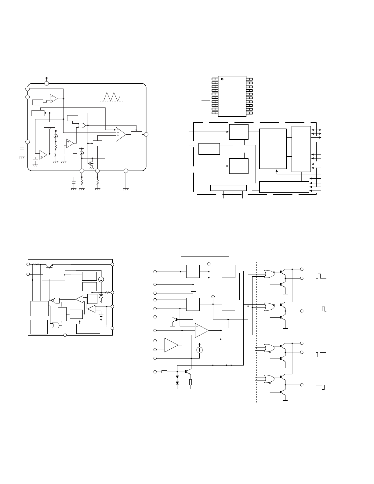
• SG2525AN (X8960A0)
PW Modulator
PSANL: IC301
V
REF
OSC.
REF.
REG.
16
U.V.
LOCK
OUT
TO INTRENAL
CIRCUITRY
OSCILLATOR
OUTPUT
4
FLIP
FLOP
R
COMP.
V
5kΩ
S
PWM
LATCH
S
REF
50µA
NOR
NOR
OR
OR
V
13
C
OUTPUT A
11
OUTPUT B
14
SG1525A OUTPUT STAGE
V
13
C
OUTPUT A
11
OUTPUT B
14
SG1527A OUTPUT STAGE
Vo
V
15
i
12
GROUND
4
ON/OFF
5
+
V
ref
VNCadj
3
SYNC.
DISCHARGE
COMP.
INV.INPUT
N.I.INPUT
SOFT-START
SHUTDOWN
3
R
6
T
C
5
T
7
9
1
ERROR
AMP.
2
8
5kΩ
10
30
Page 31

NXAMP4x1
1
2
3
4
5
6
7
8
9
10
20
19
18
17
16
15
14
13
12
11
CLR
1Q
1D
2D
2Q
3Q
3D
4D
4Q
GND
V
CC
8Q
8D
7D
7Q
6Q
6D
5D
5Q
CLK
CLK
CLR
1D
1D
3
1Q
1
11
R
C1
1D
2D
4
2Q
2
R
C1
1D
3D
7
3Q
5
R
C1
1D
4D
8
4Q
6
R
C1
1D
5D
13
5Q
9
R
C1
1D
6D
14
6Q
12
R
C1
1D
7D
17
7Q
15
R
C1
1D
8D
18
8Q
16 19
R
C1
1Y0
1Y1
1Y2
1Y3
2Y0
2Y1
2Y2
2Y3
2-COM
1-COM
13
12
14
15
11
1
5
2
4
3
INH
B
A
10
9
6
1
2
3
4
5
6
7
8
16
15
14
13
12
11
10
9
2Y2
2Y0
2-COM
2Y3
2Y1
INH
GND
GND
V
CC
1Y2
1Y1
1-COM
1Y0
1Y3
A
B
1
2
3
4
5
6
7
20
19
18
17
16
15
14
Vcc
G2
Y1
Y2
Y3
Y4
Y5
Y6
Y7
Y8
8
9
10
12
11
GND
A8
A7
A6
A5
A4
A3
A2
A1
G1
13
4B13
4A12
4Y11
3B10
3A9
3Y8
1B 2
1Y 3
2A 4
2B 5
2Y 6
GND 7
Vcc141A 1
1
DIR
A1
A2
A3
A4
A5
A6
A7
A8
GND
Vcc
OE
B1
B2
B3
B4
B5
B6
B7
B8
2
3
4
5
6
7
8
9
10
20
19
18
17
16
15
14
13
12
11
GND
Y3
A3
A2
A1
VCC
A6
A5
A4
Y6
Y5
Y4
Y2
Y1
1
2
3
4
5
6
7
14
13
12
11
10
9
8
• SN74LV273APWR (X5074A0)
D-type Flip Flop
CONTROL: IC057-061
• SN74LV4052APWR (X6976A0)
Demultiplexer
CONTROL: IC049
• SN74LVC00APWR (X5406A0)
NAND
CONTROL: IC040
• SN74LV541APWRBUS B (X5966A0)
Buffer/Driver
CONTROL: IC055, 056
PN-AN: IC001
• SN74ABT245BNSR (XU009A0)
BUS Transceiver
CONTROL: IC062
• SN74LV14APWR (X6688A0)
Inverter
CONTROL: IC063
31
Page 32

NXAMP4x1
• SN74LVC157APWR (X6786A0)
Data Selector
CONTROL: IC046, 051
1A
2
1B
A/B
GND
1A
1B
1Y
2A
2B
2Y
G
15
2
4A
14
3
4B
13
4
5
12
4Y
6
11
3A
7
10
3B
8
9
3Y
V
16
1
3
CC
2A
5
2B
6
3A
11
3B
10
4A
14
4B
13
G
15
A/B
1
• SN74LVC245APWR (XZ287A0)
Bas T r ansceiver
CONTROL: IC054
GND
1
DIR
2
A1
3
A2
4
A3
5
A4
6
A5
7
A6
8
A7
9
A8
10
20
Vcc
19
OE
18
B1
17
B2
16
B3
15
B4
14
B5
13
B6
12
B7
11
B8
• SN74LVC2G74DCTR (X8709A0)
Flip Flop
CONTROL: IC042
PRE
7
CLK
1Y
4
7
2Y
3Y
9
4Y
12
1
D
2
CLR
6
C
C
C
TG
C
C
TG
C
C
Q
TG
C
C
TG
C
5
Q
3
• TC74LCX04FT (X8415A0)
Inverter
CONTROL: IC064
VCC
14
6A
13
12
6Y
5A
11
10
5Y
9
4A
8
4Y
GND
1A
1
1Y
2
2A
3
2Y
4
3A
5
3Y
6
7
• TOP246YN 1PD (X8576A0)
Regulator
PSANL: IC201
CONTROL (1C)
EXTERNAL
CURRENT LIMIT (3X)
LINE-SENSEL (2L)
FREQUENCY (5F)
Z
C
SHUNT REGULATOR/
ERROR AMPLIFIER
I
FB
CURRENT
LIMIT
ADJUST
LINE
SENSE
R
E
V
V
V
BG+VT
BG
C
5.0V
V
I(LIMIT)
SOFT
START
ON/OFF
1 V
OVAIV
DC
MAX
6.8V
4.6V
INTERNAL UV
COMPARATOR
STOP LOGIC
STOP
DC
MAX
HALF
FREQ
OSCILLAT OR WITH JITTER
SOFTSTART
D
CLOCK
MAX
SAW
SOFT START
LIQHT LOAD
FREQUENCY
REDUCTION
+8
SHUTDOWN
AUTO-RESTART
HYSTERETIC
THERMAL
SHUTDOWN
PWM
COMPARATOR
0
1
INTERNAL
SUPPLY
DRAIN (7D)
Tab internally
connected to
SOURCE pin
CURRENT LIMIT
COMPARATOR
CONTROLLED
TURN-ON
GATE DRIVER
Q
S
R
LEADING
EDGE
BLANKING
2L
5F
3X
4S
1C
7D
32
SOURCE (4S)
Page 33

■ CIRCUIT BOARDS
CONTENTS
• CONTROL Circuit Board (X8710C0) ..........................34
• INANL Circuit Board (X8714C0) ..........................38
• LCD SPACER Circuit Board (X8711C0) ..........................41
• OPT-AN Circuit Board (X8711C0) ..........................41
• OUTANL Circuit Board (X8714C0) ..........................39
• PAANL Circuit Board (X8713D0) ..........................46
• PN-AN Circuit Board (X8711C0) ..........................42
• PSANL Circuit Board (X8715D0) ..........................47
• RS232-GPI Circuit Board (X8711C0) ..........................41
Note: See parts list for details of circuit board component parts.
NXAMP4x1
33
Page 34

NXAMP4x1
• CONTROL Circuit Board
A
to PN-AN
CN001
N.C.
to PSANL
CN313
to PSANL
CN201
to OUTANL
CN809, CN810
34
Component side
A'
2NA-WJ97120-10
2
Page 35

NXAMP4x1
A
to OUTANL
CN809, CN810
to PAANL
(CH1)
CN401
to PAANL
(CH2)
CN403
to PAANL
(CH3)
CN401
to PAANL
(CH4)
CN403
to INANL
W701
to OPT-AN
CN301
A'
2NA-WJ97120-10
to RS232-GPI
CN201
Component side
2
35
Page 36

NXAMP4x1
• CONTROL Circuit Board
B
36
Pattern side
B'
2NA-WJ97120-10
2
Page 37

NXAMP4x1
B
B'
2NA-WJ97120-10
Pattern side
2
37
Page 38

NXAMP4x1
• INANL Circuit Board
to CONTROL
CN006
DCBA
BALANCED INPUTS
Component side
38
Pattern side
2NA-WJ97320-10
Page 39

• OUTANL Circuit Board
NXAMP4x1
to PAANL (CH4)
W406 (
YELLOW
to PAANL (CH3)
W405 (
)
ORANGE
to PAANL (CH2)
W406 (
)
YELLOW
to PAANL (CH1)
W405 (
)
ORANGE
)
to PSANL
CN202
to CONTROL
to CONTROL
CN016
CN016
CN317
to PSANL
2NA-WJ97320-10
CN306
to PSANL
Speakon D Speakon C Speakon B Speakon A
POWER OUTPUTS
Component side
39
Page 40

NXAMP4x1
• OUTANL Circuit Board
40
Pattern side
2NA-WJ97320-10
Page 41

• RS232-GPI Circuit Board
to CONTROL CN10
RS232
GPIO
NXAMP4x1
Component side Pattern side
• OPT-AN Circuit Board
to CONTROL CN017
Expansion slot
Component side
• LCD SPACER Circuit Board
Component side Pattern side
Pattern side
2NA-WJ97170-10
1
41
Page 42

NXAMP4x1
• PN-AN Circuit Board
A
SELECT
PEAK
PROTECT
SIGNAL
1
MUTE
23
MUTE MUTE
42
Component side
A'
2NA-WJ97170-10
1
Page 43

NXAMP4x1
A
Encoder
4A
vol
MUTE
B
AMP PROTECT
STAND-BY
POWER
to CONTROL
CN009
A'
2NA-WJ97170-10
Component side
1
43
Page 44

NXAMP4x1
• PN-AN Circuit Board
B
44
Pattern side
B'
2NA-WJ97170-10
1
Page 45

NXAMP4x1
B
B'
2NA-WJ97170-10
Pattern side
1
45
Page 46

NXAMP4x1
• PAANL Circuit Board
to CONTROL
CN012, CN014
to OUTANL
CN805, CN807
Reduction: 9/10
A
to CONTROL
CN013, CN015
Component side
to OUTANL
CN806, CN808
A'
B
46
Pattern side
B'
2NA-WJ97310-10
1
Page 47

Reduction: 9/10
A
NXAMP4x1
A'
B
to PSANL
CN312, CN315
to PSANL CN307, CN310
to PSANL CN316, CN309
to PSANL CN305, CN308
Component side
B'
2NA-WJ97310-10
Pattern side
1
47
Page 48

NXAMP4x1
• PSANL Circuit Board
to OUTANL W802
to PAANL W404
to PAANL W402
to PAANL W401
to FUN
to CONTROL CN007
to PAANL
W403
Reduction: 7/10
A
to OUTANL CN202
to CONTROL CN011
to FUN
to PAANL CN401
to PAANL W402
to PAANL W404
to PAANL W403
to OUTANL
W805
7
6
8
5
9
4
10
3
11
2
12
1
48
Component side
B'
2NA-WJ97350-50
Page 49

Reduction: 7/10
A
NXAMP4x1
B'
2NA-WJ97350-50
Component side
49
Page 50

NXAMP4x1
• PSANL Circuit Board
Reduction: 7/10
B
50
Pattern side
B'
2NA-WJ97350-50
Page 51

Reduction: 7/10
B
NXAMP4x1
6
7
5
8
4
9
3
10
2
11
1
12
B'
2NA-WJ97350-50
Pattern side
51
Page 52

NXAMP4x1
■ TEST PROGRAM
1. Required items
Computer : DOS/V computer x1 (Pentium 200MHz or more, Windows XP, USB Port)
Software : Software for version up (JTAG Programmer)
Cable : RLINK-ST (USB-JTAG adapter)
Measuring equipment : Power consumption meter
Tools : RS-232C jig x1, GPI jig x1, SLOT jig x1
RS-232C jig
D-SUB 9 pin female connector
GPI jig
SW1
D-SUB 25 pin male connector
/ETH_CS
/ES_CS
SPI_CLK
SPI_MISO
SPI_MOSI
ES_SERIAL_RX
ES_SERIAL_TX
INT_FROM_ES
ES_GPI1
ES_GPI2
ES_GPI3
ES_I2S_DATA0
ES_I2S_DATA1
ES_MCLK
ES_SCLK
ES_LRCK
SOURCE_SEL
a-1
b-1
a-40 b-40
SLOT jig
3.3D
3.3D
XTAL
12.288MHz
Q0
Q1
LV169
Q2
Q3
Q0
Q1
LV169
Q2
Q3
2. Test connection imag e
52
SLOT, GPI, RS-232C jig
NXAMP
Measuring
instrument
Page 53

NXAMP4x1
3. Operation
3-1. Entry of the test program
While holding down the [SELECT4], [MUTE4] and [A]
buttons simultaneously, turn the power switch on. The start
up screen appears on the LCD.
Start Up Screen
Boot 1.00
WAIT...
Then release your fingers from the buttons.
The test program starts and the test menu screen appears on the LCD.
Test Menu Screen
00 CHOOSE TEST < >
01 SWITCH
3-2. Executing the test and judgment display
Select the desired test item from the table below using
the rotary encoder, and press the [B] button to start the
test.
Test Program List
01
SWITCH
02
ENCODER
03
LED
04
LCD
05
RS232
06
GPI
07
PORT (no use)
08
DSP
09
WORD CLOCK
10
12C
After executing the test, the display retur ns to the test
menu screen if the test result is OK. If an error occurs,
“ERROR” appears on the LCD and the test program is
stopped. In this case, tur n the power switch off and on
again as was done above in 3-1.
11
FLASH
12
FAN
13
SLOT
14
ATTENUATION
15
ANALOG
16
BRIDGE
17
CALIBRATION
18
STANDBY
19
QUIT
Press the switch displayed on the LCD as instructed.
If all instructed switches are OK, the display automatically returns to the test menu screen.
4-2. ENCODER test
00 CHOOSE TEST < >
02 ENCODER
Press the [B] button to start the test, and the following
display appears.
02 ENCODER
TURN RIGHT 0
Turn the ENCODER knob clockwise. The 2nd line on the
display changes as shown below.
TURN RIGHT 0 –> • • • • • –> TURN RIGHT 19
The following display appears after the 2nd line on the
display reaches TURN RIGHT 19.
02 ENCODER
TURN LEFT 0
Turn the ENCODER knob counterclockwise. The 2nd line
on the display changes as shown below.
TURN LEFT 0 –> • • • • • –> TURN LEFT 19
The display returns to the test menu screen after the 2nd
line on the display reaches TURN LEFT 19.
4-3. LED test
00 CHOOSE TEST < >
03 LED
Press the [B] button to start the test, and the following
display appears.
4. Outline of tests
4-1. SWITCH test
00 CHOOSE TEST < >
01 SWITCH
Press the [B] button to start the test. The LCD shows one
by one the switch name to be tested as shown below.
01 SWITCH
HIT SELECT CH1
03 LED
The LEDs automatically light up one by one in a specific
order as shown on the next page.
All LEDs will light at the same time after each LED individually has been tested. Confirm that each LED is lit
normally. If OK, press the [B] button to return the display
to the test menu screen.
53
Page 54

NXAMP4x1
Lighting order
4-4. LCD test
00 CHOOSE TEST < >
04 LCD
Press the [B] button to start the test.
First the following display appears.
04 LCD
All the dots of the LCD go on and off two times. Finally, all
the dots of the LCD are lit. Confirm that all the dots of the
LCD have lit normally. If OK, press the [B] button to return the display to the test menu screen.
4-5. RS-232C test
00 CHOOSE TEST < >
05 RS-232C
Connect the RS-232C jig to the R232C port of the
NXAMP4x1.
Then press the [B] button to start the test, and the following display appears.
05 RS-232C
RS-232C OK ?
Press the [B] button to continue the test. The test e xecutes
automatically.
After executing the test, the following display appears.
(When an error occurs, the “ERROR” appears and the
test program is stopped.)
05 RS-232C
RELEASE RS-232C
Disconnect the RS-232C jig from the RC232C port. Press
the [B] button to return the display to the test menu screen.
4-6. GPI test
00 CHOOSE TEST < >
06 GPI
Connect the GPI jig to the GPIO port of the NXAMP4x1.
Then press the [B] button to start the test, and the following display appears.
06 GPI
GPO[0:4] TEST OK ?
Switch the GPI jig to the GPO [0:4] position and press
the [B] button to continue the test.
The test executes automatically.
If normal, the following display appears. (If an error occurs, “ERROR” appears and the test program is stopped.)
54
06 GPI
GPO[5:7] TEST OK ?
Page 55

NXAMP4x1
Switch the GPI jig to the GPO [5:7] position. Press the
[B] button to continue the test.
The test executes automatically. If the test result is OK,
the display automatically returns to the test menu screen.
(If an error occurs, “ERROR” appears and the test pro-
gram is stopped.)
Disconnect the GPI jig from the GPIO port.
4-7. PORT test
Test for factory inspection only.
4-8. DSP test
00 CHOOSE TEST < >
08 DSP
Press the [B] button to start test. The following display
appears.
08 DSP
CPU to DSP TEST OK ?
Press the [B] button to continue the test. The test e xecutes
automatically.
If normal, the following display appears.
Press the [B] button to start the test. The following display appears.
09 WORD CLOCK
LRCK 48k TEST OK ?
Press the [B] button to continue the test. The test is executed automatically.
If normal, the following display appears.
09 WORD CLOCK
LRCK 96k TEST OK ?
Press the [B] button to continue the test. The test is executed automatically.
If the test result is OK, the display automatically returns
to the test menu screen.
(If an error occurs, “ERROR” appears and the test pro-
gram is stopped.)
4-10. 12C test
00 CHOOSE TEST < >
10 12C
08 DSP
DSP to DSP TEST OK ?
Press the [B] button to continue the test. The test e xecutes
automatically.
If the test result is OK, the display automatically returns
to the test menu screen.
(If an error occurs, “ERROR” appears and the test pro-
gram is stopped.)
4-9. WORD CLOCK test
00 CHOOSE TEST < >
09 WORD CLOCK
Press the [B] button to start the test. The following display appears.
10 12C
12C TEST OK ?
Press the [B] button to continue the test. The test e xecutes
automatically.
If the test result is OK, the display automatically returns
to the test menu screen.
(If an error occurs, “ERROR” appears and the test pro-
gram is stopped.)
55
Page 56

NXAMP4x1
4-11. FLASH test
00 CHOOSE TEST < >
11 FLASH
Press the [B] button to start the test. The following display appears.
11 FLASH
FLASH TEST OK ?
Press the [B] button to continue the test. The test e xecutes
automatically.
If the test result is OK, the display automatically returns
to the test menu screen.
(If an error occurs, “ERROR” appears and the test pro-
gram is stopped.)
4-12. FAN test
00 CHOOSE TEST < >
12 FAN
Press the [B] button to start the test. The following display appears.
The FAN starts rotating at low speed.
12 FAN
LOW
Check that the FAN rotates at low speed, and press the
[B] button to continue the test. The following display appears, and the FAN rotates at middle speed.
12 FAN
MIDD
4-13. SLOT test
00 CHOOSE TEST < >
13 SLOT
Rear panel
(Remove the [610] plate on the rear panel of the NXAMP4x1,
and insert the SLOT jig into the expansion slot.)
Press the [B] button to start the test. The test executes
automatically.
If every signal is normal, the following display appears
and the LED of the SLOT jig lights.
(If an error occurs, “ERROR” appears and the test pro-
gram is stopped.)
[610]
13 SLOT
ANALOG TEST OK ?
Input the 1 kHz, -10 ± 1 dBu sine wave to the channel 1
input terminal and confirm that the output voltage obtained
at the channel 1 output terminal is +19.1 ± 2.0 dBu.
If OK, press the [B] button to return the display to the test
menu screen.
4-14. ATTENUATION test
00 CHOOSE TEST < >
14 ATTENUATION
Check that the FAN rotates at middle speed, and press
the [B] button to continue the test. The following display
appears, and the FAN rotates at high speed.
12 FAN
HIGH
Check that the FAN rotates at high speed, and press the
[B] button to return the display to the test menu screen.
56
Press the [B] button to enter the attenuation test mode.
The following display appears.
14 ATTENUATION
NOISE TEST OK ?
Perf orm the test according to the “Inspection with attenuation test mode”. (See page 60).
If OK, press the [B] button to return the display to the test
menu screen.
Page 57

NXAMP4x1
4-15. ANALOG test
00 CHOOSE TEST < >
15 ANALOG
Press the [B] button to enter the analog test mode. The
following display appears.
15 ANALOG
ANALOG TEST OK ?
Perform the test according to the “Inspection with analog
test mode”. (See page 61, 62).
Press the [B] button. The following display appears.
15 ANALOG
MUTE TEST OK ?
If OK, press the [B] button to return the display to the test
menu screen.
4-16. BRIDGE test
00 CHOOSE TEST < >
16 BRIDGE
Press the [B] button to enter the bridge test mode. The
following display appears.
16 BRIDGE
ANALOG TEST OK ?
Input the 1 kHz, +10 dBu sine wave to the channel 2 input terminal, and press the [B] button. The analog input
level is automatically calibrated, and the following display appears.
17 CALIBRATION
CH3 INPUT SIGNAL OK ?
Input the 1 kHz, +10 dBu sine wave to the channel 3 input terminal, and press the [B] button. The analog input
level is automatically calibrated, and the following display appears.
17 CALIBRATION
CH4 INPUT SIGNAL OK ?
Input the 1 kHz, +10 dBu sine wave to the channel 4 input terminal, and press the [B] button. The analog input
level is automatically calibrated, and the following display appears.
17 CALIBRATION
CH1 SET TO 39.1 dBu ?
Input the 1 kHz, +10 dBu sine wave to the channel 1 input terminal.
Adjust the ENCODER so that the output voltage obtained
at the channel 1 output terminal is +39.1 dBu, and press
the [B] button.
The analog output level is automatically calibrated, and
the following display appears.
Perf orm the test according to the “Inspection with BRIDGE
mode”. (See page 63).
If OK, press the [B] button to return the display to the test
menu screen.
4-17. CALIBRATION
00 CHOOSE TEST < >
17 CALIBRATION
Press the [B] button to start the calibration. The following
display appears.
17 CALIBRATION
CH1 INPUT SIGNAL OK ?
Input the 1 kHz, +10 dBu sine wave to the channel 1 input terminal, and press the [B] button. The analog input
level is automatically calibrated, and the following display appears.
17 CALIBRATION
CH2 INPUT SIGNAL OK ?
17 CALIBRATION
CH2 SET TO 39.1 dBu ?
Input the 1 kHz, +10 dBu sine wave to the channel 2 input terminal.
Adjust the ENCODER so that the output voltage obtained
at the channel 2 output terminal is +39.1 dBu, and press
the [B] button.
The analog output level is automatically calibrated, and
the following display appears.
17 CALIBRATION
CH3 SET TO 39.1 dBu ?
Input the 1 kHz, +10 dBu sine wave to the channel 3 input terminal.
Adjust the ENCODER so that the output voltage obtained
at the channel 3 output terminal is +39.1 dBu, and press
the [B] button.
The analog output level is automatically calibrated, and
the following display appears.
17 CALIBRATION
CH4 SET TO 39.1 dBu ?
57
Page 58

NXAMP4x1
Input the 1 kHz, +10 dBu sine wave to the channel 4 input terminal.
Adjust the ENCODER so that the output voltage obtained
at the channel 4 output terminal is +39.1 dBu, and press
the [B] button.
The analog output level is automatically calibrated, and
the following display appears.
17 CALIBRATION
CH1 OUTPUT SIGNAL OK ?
Adjust the input signal voltage so that the output voltage
obtained at the channel 1 output terminal is 24 Vrms (=
+29.8 dBu), and press the [B] button.
The output voltage monitor is automatically calibrated,
and the following display appears.
17 CALIBRATION
CH2 OUTPUT SIGNAL OK ?
Adjust the input signal voltage so that the output voltage
obtained at the channel 2 output terminal is 24 Vrms (=
+29.8 dBu), and press the [B] button.
The output voltage monitor is automatically calibrated,
and the following display appears.
17 CALIBRATION
CH3 OUTPUT SIGNAL OK ?
Adjust the input signal voltage so that the output voltage
obtained at the channel 3 output terminal is 24 Vrms (=
+29.8 dBu), and press the [B] button.
The output voltage monitor is automatically calibrated,
and the following display appears.
17 CALIBRATION
CH4 OUTPUT SIGNAL OK ?
Adjust the input signal voltage so that the output voltage
obtained at the channel 4 output terminal is 24 Vrms (=
+29.8 dBu), and press the [B] button.
The output voltage monitor is automatically calibrated,
and the following display appears.
17 CALIBRATION
CH1 CONNECT 8 OHM LOAD
Connect the 8 ohms resistor to the channel 1 output terminal.
Adjust the input signal voltage so that the output voltage
obtained at the channel 1 output terminal is 24 Vrms (=
+29.8 dBu), and press the [B] button.
The output current monitor is automatically calibrated,
and the following display appears.
17 CALIBRATION
58
CH2 CONNECT 8 OHM LOAD
Connect the 8 ohms resistor to the channel 2 output terminal.
Adjust the input signal voltage so that the output voltage
obtained at the channel 2 output terminal is 24 Vrms (=
+29.8 dBu), and press the [B] button.
The output current monitor is automatically calibrated,
and the following display appears.
17 CALIBRATION
CH3 CONNECT 8 OHM LOAD
Connect the 8 ohms resistor to the channel 3 output terminal.
Adjust the input signal voltage so that the output voltage
obtained at the channel 3 output terminal is 24 Vrms (=
+29.8 dBu), and press the [B] button.
The output current monitor is automatically calibrated,
and the following display appears.
17 CALIBRATION
CH4 CONNECT 8 OHM LOAD
Connect the 8 ohms resistor to the channel 4 output terminal.
Adjust the input signal voltage so that the output voltage
obtained at the channel 4 output terminal is 24 Vrms (=
+29.8 dBu), and press the [B] button.
The output current monitor is automatically calibrated,
and the display returns to the test menu screen.
(If an error occurs, “ERROR” appears and the test pro-
gram is stopped.)
4-18. STANDBY test
00 CHOOSE TEST < >
18 STANDBY
Press the [B] button to enter the standby mode, and the
following display appears.
18 STANDBY
Measure the primary power consumption, and check that
the measured value is 23 W or less. Press the [B] button
for one second or more, and the display retur ns to the
test menu screen.
4-19. QUIT (Exit the test program)
00 CHOOSE TEST < >
19 QUIT
Press the [B] button to exit the test program, and the
NXAMP enters the ordinary mode.
Page 59

■ INSPECTIONS
1. Measurement Conditions
1-1. Environment
• Normal temperature: From 10 ˚C to 35 ˚C
• Normal humidity: From 45 % to 85 %
1-2. Power Source
• When measuring the electrical characteristics, set the power supply voltage and frequency as specified in the tab le below.
Destination
U
CHN
1-3. Measuring Instruments
• Use a reliable measuring device capable of precisely measuring the specification values indicated in this document.
• Input impedance of the measuring instrument should be more than 1 MΩ.
• The noise level should be measured with a 22 Hz-22 kHz band pass filter.
When you use the Audio Analyzer System made by Audio Precision, Inc. for noise measurement, set the filter characteristics as follows.
BW : 22 Hz-22 kHz
Filter (Fltr) : None
Power supply voltage
120 V +2/-0 %
230 V +2/-0 %
Frequency
60 Hz
50 Hz
NXAMP4x1
1-4. Connections
Each input and output terminal of channels 1-4 are as shown in the figure below.
Ch4
OUT
Ch3
OUT
Ch2
OUT
Ch1
OUT
Ch3INCh2INCh1
Ch4
IN
Ch4
Ch3
LINK
LINK
OUT
OUT
Ch2
LINK
OUT
Fig. 1
1-4-1. Input connector
The XLR-3-31 (female) type connectors are used for channel 1-4 input terminals.
Condition : Balanced input
Wiring : pin 1 to ground, pin 2 to hot (+), pin 3 to cold (-)
1-4-2. Output connector
Neutrik SPEAKON connectors are used for output terminals in channels 1-4.
Connect the load resistor between pin 1+ and pin 1- of the Neutrik SPEAKON connector.
1-4-3. Load resistor
Use a load resistor with no inductivity and a power rating high enough to perform each test safely.
IN
Ch1
LINK
OUT
1-4-4. Link out connectors
XLR-3-32 (male) type connectors are used for input terminals in channels 1-4.
Condition : Balanced output
Wiring : pin 1 to ground, pin 2 to hot (+), pin 3 to cold (-)
59
Page 60

NXAMP4x1
1-5. Other
0 dBu is defined as 0.775 Vrms in these inspections.
2. Inspection with ordinary mode
Condition:
• Ground each input terminal via a 600 Ω resistor.
• Do not connect the load resistor to the output terminal.
2-1. Power ON sequence
1) Turn the power switch on. Confirm that the latest firmware version appears on the LCD and the four (4) MUTE LEDs light
up.
Example of firmware version 1.00
-- [v 1.00] --
(c) NEXO 2007.
2) Confirm that all the fans start rotation at low speed within 4 seconds after turning the power switch on.
3) Confirm that the following display appears on the LCD within 18 ± 3 seconds after turning the power switch on. Also
confirm that the POWER LED and only one of the VOLUME LEDs for each channel light up.
-20.0 -20.0 -20.0 -20.0 Vol(dB)
[MAIN ][MAIN ][SUB ][SUB ] < >
2-2. Power consumption when idling
Measure the primary power consumption and confirm that the measured value is 70 ± 20 W.
2-3. Output terminal DC voltage
Measure the DC voltage (Vdc) of each output terminal and confirm that the measured value is Vdc = 0 ± 50 mV.
3. Inspection with attenuation test mode
Condition:
• Perform each test in this section in the attenuation test mode. (See page 56)
• Connect a 8 Ω load resistor to each output terminal.
• Ground each input terminal via a 600 Ω resistor.
3-1. Residual noise
Confirm that each output terminal’ s residual noise level is -65 dBu or less.
60
Page 61

4. Inspection with analog test mode
Condition:
• Perform each test item in this section with the analog test mode of the test program. (See page 57)
• Unless otherwise specified, perform the test with a 8 Ω resistor is connected to each output terminal.
4-1. Link out
Input the 1 kHz, -10 dBu sine wav e to each input terminal and confirm that the output voltage obtained at each link out terminal
is -10 ± 0.5 dBu.
4-2. Efficiency
Input the 1 kHz sine wave to the channel 1 input terminal and confirm that the primary power consumption is 175 ± 10 W when
the output voltage obtained at the channel 1 output terminal is +29.2 dBu.
Perform the same test for channels 2-4 in the same manner.
4-3. Gain
Input the 1 kHz, 0 dBu sine wave to each input terminal and confirm that the output voltage obtained at each output terminal
is +29.1 ± 1.2 dBu.
NXAMP4x1
4-4. Frequency response
Perform the following test at each channel.
Input the 10 Hz, 1 kHz, 20 kHz, 0 dBu sine wave to the input terminal and one by one measure the output voltage obtained at
the output terminal for each frequency.
Confirm that the output voltage at 10 Hz is 0 ± 0.5 dB when compared with the output voltage at 1 kHz (0 dB).
Confirm that the output voltage at 20 kHz is +0.5 ± 0.5 dB when compared with the output voltage at 1 kHz (0 dB).
4-5. Distortion
Input the 1kHz sine wave to each channel input terminal and confirm that the distortion in each channel output terminal is 1.0
% or less when 500 W (with 8 ohms load) output is obtained for each terminal at the same time.
4-6. Maximum output
Connect the 4 ohms 500 W resistor to each output terminal.
Input the BURST signal as shown in fig. 2 to each input terminal and adjust the input signal le vel so that a Vburst voltage of 174
Vp-p (volt peak to peak) is obtained in each channel output terminals.
Measure the last wave of the BURST signal peak to peak by the oscilloscope's MEASURE function. Confirm that the measured voltage is 170 volt or more. (See fig. 2)
Note: Perform the test of all channels at the same time.
500 msec
1 msec
20 msec
Close-up
The center of the emission line shall
be adopted as the measurement value.
Signal
Cursor
Fig. 2
Vburst
The last one wave of burst signal
shall be measured.
61
Page 62

NXAMP4x1
4-7. Channel separation
1) Ground the channel 2, channel 3 and channel 4 input terminals via a 600 Ω resistor.
Input the 1 kHz, 0 dBu sine wave to the channel 1 input terminal and measure the output voltage obtained at the channel
1 output terminal as the reference voltage (0 dB).
Confirm that the output voltage at the channel 2, channel 3 and channel 4 output terminals is -65 dB or less as compared
with the reference voltage.
2) Ground the channel 1, channel 3 and channel 4 input terminals via a 600 Ω resistor.
Input the 1 kHz, 0 dBu sine wave to the channel 2 input terminal and measure the output voltage obtained at the channel
2 output terminal as the reference voltage (0 dB).
Confirm that the output voltage at the channel 1, channel 3 and channel 4 output terminals is -65 dB or less as compared
with the reference voltage.
3) Ground the channel 1, channel 2 and channel 4 input terminals via a 600 Ω resistor.
Input the 1 kHz, 0 dBu sine wave to the channel 3 input terminal and measure the output voltage obtained at the channel
3 output terminal as the reference voltage (0 dB).
Confirm that the output voltage at the channel 1, channel 2 and channel 4 output terminals is -65 dB or less as compared
with the reference voltage.
4) Ground the channel 1, channel 2 and channel 3 input terminals via a 600 Ω resistor.
Input the 1 kHz, 0 dBu sine wave to the channel 4 input terminal and measure the output voltage obtained at the channel
4 output terminal as the reference voltage (0 dB).
Confirm that the output voltage at the channel 1, channel 2 and channel 3 output terminals is -65 dB or less as compared
with the reference voltage.
Note: Measure the output level with the 22 Hz-22 kHz band pass filter specified at 1-3.
4-8. Output noise level
With each input terminal grounded via a 600 Ω resistor, measure the noise le vel in each output terminal and confirm that the
measured value is -60 dBu or less.
Note: Measure the noise level with the 22 Hz-22 kHz band pass filter specified at 1-3.
4-9. Stability
With no load resistors connected to all output terminals, input the 1 kHz, -6.0 dBu square wave and measure the primary
power consumption (Wno_load).
With the 0.1 uF capacitor connected to all output terminals, input the 1 kHz, -6.0 dBu square wave and measure the primary
power consumption (Wcap_load).
Confirm that the following equation is satisfied.
Wcap_load-Wno_load = 10 W or less
62
Page 63

5. Inspection with BRIDGE mode
Condition:
• Perform each test item in this section with the bridge test mode of the test program. (See page 57)
• Connect individually the 16 Ω load resistors to channel 1 and channel 3 output terminals.
• Keep the measurement reference of the measuring instrument in floating condition and connect it to the middle point of
each load resistors.
• Do not connect any resistor to channel 2 and channel 4 output terminals.
• The input terminals and output terminals of channel 2 and channel 4 are not used in this section.
5-1. Gain
Input the 1 kHz, 0 dBu sine wave to each input terminal and confirm that the output voltage obtained at each output terminal
is +29.1 ± 1.2 dBu.
5-2. Frequency response
Perform the following test at each channel.
Input the 10 Hz, 1 kHz, 20 kHz, 0 dBu sine wave to the input terminal and one by one measure the output voltage obtained at
the output terminal for each frequency.
Confirm the output voltage at 10 Hz is 0 ± 0.5 dB when compared with the output voltage at 1 kHz (0 dB).
Confirm the output voltage at 20 kHz is +0.5 ± 0.5 dB when compared with the output voltage at 1 kHz (0 dB).
NXAMP4x1
63
Page 64

NXAMP4x1
■ UPDA TING THE FIRMWARE
1. Preparation
1-1. Downloading and installing the software for update
1) Download http://www.st.com/stonline/products/support/micro/files/standalone_jtag.zip.
2) Extract the StandaloneJTAG_1_20.zip.
3) Double click the StandaloneJTAG_1_20, and the following
install screen appears. (Fig. 1)
4) Click the [Finish] button to start installing the software for
update.
5) Click the [Next] and [Yes] buttons to finish installing.
6) Restart the PC after completing the installation.
1-2. Connection
Connect the USB port of the PC to the connector CN005 of the
CONTROL circuit board installed in the NXAMP4x1 with the USBJTAG adapter (RLINK-ST).
Note:
When you connect the USB-JTAG adapter (RLINK-ST) for the
first time, the USB driver will be required. The USB driver is included in the downloaded file at previous step 1-1. Locate and
install the driver.
Fig. 1 Install screen
2. Updating operation
1) Turn the power switch of the NXAMP on.
2) Start up the installed JTAG Programmer.
3) Select new project from the project menu. The following “Create Project” screen appears. (Fig. 2)
4) Input the Project Name, Device Family and Device Name as the followings.
Project Name : an (any name may be used)
Device Family : uPSD3300
Device Name : uPSD3354DV-40U6
64
Fig. 2 Create Project screen
Page 65

NXAMP4x1
5) Click the [Create] button, and the following JTAG Programmer screen appears. (Fig. 3)
6) Click the [Browse] button to select the desired file.
Check the [All] at Select region.
Select Program/Verify at Select operation.
Note:
This operation is needed when you start up for the first time. Click the [Save] button to sav e the set up file so that this operation
will not be required again.
Fig. 3 JTAG Programmer screen
7) Click the [HW Setup] button, and the following hardware setting screen appears. (Fig. 4)
8) Select the RLink at Hardware selection.
Fig. 4 Hardware Setting screen
9) Click the [Execute] button, and the following JTAG-ISP Operations screen appears. (Fig. 5)
Fig. 5 JTAG-ISP Operations screen
10) Click the [
11) Restart the PC after the completion of the updating.
Yes] button to start updating the firmware.
65
Page 66

PAR TS LIST
■ CONTENTS
OVERALL ASSEMBLY 1/2.................................................................... 2
2/2.................................................................... 4
PA UNIT .................................................................................................. 6
LCD ASSEMBLY .................................................................................... 8
LOCATIONS OF HEAT SINK UNITS ..................................................... 9
HEAT SINK UNIT L100 ........................................................................ 10
HEAT SINK UNIT L100 ........................................................................ 11
HEAT SINK UNIT L60 .......................................................................... 12
HEAT SINK UNIT L60 .......................................................................... 13
HEAT SINK UNIT L50 .......................................................................... 14
HEAT SINK UNIT OSH ........................................................................ 15
ELECTRICAL PARTS ............................................................................ 16
NXAMP4x1
Notes: DESTINATION ABBREVIATIONS
CHN : Chinese model U: U.S.A. model
■ WARNING
Components having special characteristics are marked and must be replaced with par ts having
specification equal to those originally installed.
• The numbers “QTY” show quantities for each unit.
• The parts with “--” in “PART NO.” are not available as spare parts.
• This mark “ } ” in the REMARKS column means these parts are interchangeable.
• The second letter of the shaded ( ) part number is O, not zero.
• The second letter of the shaded ( ) part number is I, not one.
Page 67

NXAMP4x1
■ OVERALL ASSEMBLY 1/2
650
650
640
650
670
660
660
400
425
430
420
340
390
430
370
380
350
360
620
610
650
410
660
590
530
600
110
110a
540
570
510
540
590
545
560
580
450
550
510
500
490
455
460
505
480
440
500
LCD Assembly
470
(See page 8)
670
660
Bottom section
(See page 4)
630
2
Page 68

NXAMP4x1
OVERALL ASSEMBLY
Overall Assembly AN-PA-LOW U (WK66600)
--
Overall Assembly AN-PA-LOW CHN CHN (WK66620)
s 110 Connector Assembly SWPS VH3P AWG22 SW POWER (WK94710)
s 110a See-Sow Switch JW-M21RKK-NOD POWER SWITCH (WK75450)
340 Hexagonal Spacer H=20 B=5.5 (WK67210) 2
350 Cord Binder T18R TYTIN CO. (V327280) 9
* 360 OPT Angle AN-PA
370 Circuit Board OPT-AN (WJ97150)
380 Bind Head Tapping Screw-S 3x6 MFZN2W3 (WE87790) 2
390 FFC Cable SMCD 40P 70mm (WK02120)
400 Bind Head Tapping Screw-S 3x6 MFZN2W3 (WE87790) 3
410 Bind Head Tapping Screw-S 3x6 MFZN2B3 (WE87780) 2
* 420 Circuit Board CONTROL
425 Cushion Control AN-PA (WN15950)
430 Bind Head Tapping Screw-S 3x6 MFZN2W3 (WE87790) 4
440 Sub Chassis AN-PA (WK14900)
450 Bind Head Tapping Screw-S 3x6 MFZN2W3 (WE87790) 3
455 Cushion Front AN-PA (WN19370) 3
* 460 Front Panel AN-PA-LOW
470 LCD Assembly PA 8F27_8F28 (WK75670)
480 FFC Cable SMCD 30P 210mm (WK02100)
490 Push Button AN-PA SELECT-CH1,SELECT-CH2, 6
500 Bind Head Screw 3x4 MFZN2B3 (WF10570) 5
505 Dust Guard (WN41240)
510 Flat Head Screw 4x8 MFZN2B3 (WE98030) 8
530 Front Panel 2 AN-PA-LOW
540 Adhesive Tape #5000NS W=5mm (WG94020)
545 Double Sided Adhesive Tape 15P LM (WM78140) 4
* 550 LCD Cover AN-PA
* 560 Level Meter 15P CH1,CH2,CH3,CH4 4
* 570 LED Lens 2P 7
* 580 Lens Button AN-PA MUTE-CH1,MUTE-CH2, 4
590 Bind Head Tapping Screw-S 3x6 MFZN2B3 (WF05470) 8
* 600 Encoder Knob AN-PA ENCODER
610 Plate AN-PA (WK67780)
620 Bind Head Tapping Screw-S 3x6 MFZN2B3 (WE87780) 2
630 Cord Binder T18R TYTIN CO. (V327280) 9
640 Top Cover AN-PA-LOW U U (WK67010)
640 Top Cover AN-PA-LOW CHN CHN (WK67020)
650 Bind Head Screw 4x8 MFZN2B3 (WE96200) 13
660 Screw Cover T5N (WJ61830) 8
670 Bind Head Tapping Screw-B 3x8 MFZN2B3 (WE77440) 8
: New Parts RANK: Japan only
--
--
--
--
--
WK671500
--
--
--
--
--
WK044100
--
--
--
--
--
WK670500
--
--
WK673500
--
--
--
WK690800
--
-WK585400
WA587301
WA773701
WK585300
-WN002600
--
--
--
--
--
--
--
--
総組立
総組立
総組立
総組立
総組立
総組立
総組立
総組立
総組立
総組立
総組立
総組立
総組立
総組立
総組立
総組立
総組立
総組立
総組立
ボトムAssy
PST5シート
PST5シート
PST5シート
PST5シート
PST4シート
PST4シート
PST4シート
PST4シート
PST3シート
PST3シート
PST3シート
PST3シート
絶縁シート
Bタイト+BIND
CPUT5シート
CPUT4シート
CPUT3シート
Bタイト+BIND
防振ゴム
束線#28
カード電線C&C
ACアングル
ACアングル
Bタイト+BIND
電源コードセット
電源コードセット
電源コードセット
電源コードセット
電源コードセット
コードストッパー
コードストッパー
小ネジ+BIND
PAユニット
PAユニット
サイドカバーL 塗装
サイドカバーR 塗装
平座みがき丸
Bタイト+BOND
ネジカバー
Bタイト+BIND
束線IN
束線IN3
束線TE
Bタイト+BOND
フロントAssy
フロントAssy
フロントAssy
フロントAssy
フロントAssy
フロントAssy
SELECT-CH3,SELECT-CH4,
VOL-A,VOL-B
MUTE-CH3,MUTE-CH4
RANK部品名 QTYREMARKSDESCRIPTIONREF NO. PART NO.
3
Page 69

NXAMP4x1
■ OVERALL ASSEMBLY 2/2
PA Unit
190
(See page 6)
200
50
40
50
30
20
100
130
220
185
120
210
80
20
100
90
180
170
330
95
100
160
75
280
290
70
320
310
60
150
140
140a
20
250
300
277
285
270
276
275
274
273
240
40
10
20
50
30
50
225
260
PA Unit
230
(See page 6)
4
Page 70

NXAMP4x1
* 10 Main Chassis AN-PA-LOW U U
* 10 Main Chassis AN-PA-LOW CHN CHN
* 80 Circuit Board PSANL U
* 80 Circuit Board PSANL CHN
* 190 PA Unit AN-PA-LOW 8F27
* 230 PA Unit AN-PA-LOW 8F27
s Power Cord Assembly UL18A U
s AC Cord CHN 3 2.5m CHN
WK668500
WK668600
20 Bind Head Screw 4x8 MFZN2B3 (WE96200) 4
30 DC Fan FBA08A24H1TZ 2
40 Bind Head Screw 4x35 MFZN2W3 SP (WG16730) 4
50 Hexagonal Nut M4 #1 (WG16920) 4
60 Circuit Board INANL (WJ97270)
70 Bind Head Tapping Screw-B 2.6x8 MFZN2B3 (WE96170) 16
75 Insulation Sheet PS AN-PA (WM98090)
90 Hexagonal Spacer H=89 B=5.5 (WK67180)
95 Hexagonal Spacer H=41 B=5.5 (WN00250)
100 Bind Head Tapping Screw-S 3x6 MFZN2W3 (WE87790) 9
120 Connector Assembly PH11P C&C 11P 200mm (WK68760)
130 Connector Assembly PH9P C&C 9P 200mm (WK68770)
140 Connector Assembly ACPS 20A POWERCON ASS’Y U (WK66050)
140a AC Connector NAC3MPA U (WK66030)
140 Connector Assembly ACPS AC INLET ASS’Y CHN (WK66040)
140a AC Inlet AP-300-3- CHN (WF40880)
150 Flat Head Tapping Screw-B 3x8 MFZN2B3 U (WF26680) 2
150 Bind Head Tapping Screw-B 3x8 MFZN2B3 CHN (WE77440) 2
160 Bind Head Tapping Screw-S 4x8 MFZN2W3 (WE94180)
170 Ferrite Core K1 NFT-13BK2 (V312290)
180 Cord Binder T18R TYTIN CO. U (V327280) 2
180 Cord Binder T18R TYTIN CO. CHN (V327280)
185 Adhesive Cloth Tape 15x30 (WG52680)
200 Connector Assembly SIG-PA1 C&C 5P 420mm (WK02080)
210 Wiring Assembly C&C 5P 420mm (WK90770)
220 Bind Head Screw 4x8 MFZN2B3 (WE96200) 6
225 Adhesive Cloth Tape 15x30 (WG52680)
240 Wiring Assembly C&C 5P 500mm (WK90790)
250 Connector Assembly SIG-PA4 C&C 5P 500mm (WK17110)
260 Bind Head Screw 4x8 MFZN2B3 (WE96200) 6
270 Circuit Board OUTANL (WJ97290)
273 Insulation Sheet 1 AN-PA (WM14990)
274 Shield 1 AN-PA (WM14970)
275 Shield 2 AN-PA (WM14980)
276 Insulation Sheet 2 AN-PA (WM15000)
277 Plastic Rivet NRP-345 (CB81574) 3
280 Flat Head Tapping Screw-B 3x8 MFZN2B3 (WF26680) 8
285 Bind Head Tapping Screw-S 3x6 MFZN2W3 (WE87790)
290 Bind Head Tapping Screw-B 3x8 MFZN2B3 (WE77440)
300 Connector Assembly SENS SENSE (WK02090)
310 Circuit Board RS232-GPI (WJ97140)
320 FFC Assembly WK02110,SUMITUBE (WM15830)
330 Hexagonal Lock Screw (WK51890) 4
: New Parts RANK: Japan only
--
V8746701
--
--
--
--
-WJ974100
WJ974200
--
--
--
--
--
--
--
--
--
--
--
--
--
--
--
-WJ949600
--
--
--
-WJ949600
--
--
--
--
--
--
--
--
--
--
--
--
--
--
--
--
ACCESSORIES
WK602800
WC901301
総組立
総組立
総組立
総組立
総組立
総組立
総組立
総組立
総組立
総組立
総組立
総組立
総組立
総組立
総組立
総組立
総組立
総組立
総組立
ボトムAssy
PST5シート
PST5シート
PST5シート
PST5シート
PST4シート
PST4シート
PST4シート
PST4シート
PST3シート
PST3シート
PST3シート
PST3シート
絶縁シート
Bタイト+BIND
CPUT5シート
CPUT4シート
CPUT3シート
Bタイト+BIND
防振ゴム
束線#28
カード電線C&C
ACアングル
ACアングル
Bタイト+BIND
電源コードセット
電源コードセット
電源コードセット
電源コードセット
電源コードセット
コードストッパー
コードストッパー
小ネジ+BIND
PAユニット
PAユニット
サイドカバーL 塗装
サイドカバーR 塗装
平座みがき丸
Bタイト+BOND
ネジカバー
Bタイト+BIND
束線IN
束線IN3
束線TE
Bタイト+BOND
フロントAssy
フロントAssy
フロントAssy
フロントAssy
フロントAssy
フロントAssy
RANK部品名 QTYREMARKSDESCRIPTIONREF NO. PART NO.
5
Page 71

NXAMP4x1
■ PA UNIT
60
10
20
60
50
50
70
20
30
40
80
60
40
60
Q526
D506 Q524
Q512P Q510P
D503
Q518Q522 Q511P Q509P
D504 Q520
Q506P
Q508P
Q502P
Q504P
Q506N
Q508N
Q502N
Q504N
Q514
Q517
FRONT REAR
D505
Q525
Q523
Q521
Q521N
Q511N
Q510N
Q509N
D502
D501
Q519
Q516
Q507P
Q505P
Q503P
Q501P
Q507N
Q505N
Q503N
Q501N
Q515 IC501
Q513
6
Page 72

NXAMP4x1
WJ949600
10 Heat Sink AN-PA-LOW (WJ94980)
20 Hexagonal Spacer H=7.5 B=5.5 (WD49000) 6
30 Circuit Board PAANL (WJ97250)
40 Bind Head Tapping Screw-S 3x6 MFZN2W3 (WE87790) 6
50 Insulation Sheet PA-L TBM51W T=0.15 (WK11930) 2
60 Bind Head Screw 3x12 MFZN2W3 SP (WE87770) 44
70 Insulation Bushing 2.6M (WA00920)
80 Bind Head Screw 2.6x8 MFZN2W3 SP (WE96770)
D501 Diode SF20L60U (V635170)
D502 Diode SF20L60U (V635170)
D503 Diode SF20L60U (V635170)
D504 Diode SF20L60U (V635170)
D505 Diode SF20L60U (V635170)
D506 Diode SF20L60U (V635170)
IC501 IC LM35DT THERMO SENSOR (X0670A0)
Q513 Transistor 2SA1668A LFNO.600
WJ461500
Q514 Transistor 2SA1668A LFNO.600
WJ461500
Q515 Transistor 2SC4382A LFNO.600
WJ461600
Q516 Transistor 2SA1668A LFNO.600
WJ461500
Q517 Transistor 2SC4382A LFNO.600
WJ461600
Q518 Transistor 2SA1668A LFNO.600
WJ461500
Q519 Transistor 2SC4382A LFNO.600
WJ461600
Q520 Transistor 2SA1668A LFNO.600
WJ461500
Q521 FET 2SK3003
V8093501
Q522 FET 2SK3003
V8093501
Q523 FET 2SK3003
V8093501
Q524 FET 2SK3003
V8093501
Q525 FET 2SK3003
V8093501
Q526 FET 2SK3003
V8093501
Q501N Pair T ransistor A1492A/C3856A
V8094901
Q501P Pair T ransistor A1492A/C3856A
V8094901
Q502N Pair T ransistor A1492A/C3856A
V8094901
Q502P Pair T ransistor A1492A/C3856A
V8094901
Q503N Pair T ransistor A1492A/C3856A
V8094901
Q503P Pair T ransistor A1492A/C3856A
V8094901
Q504N Pair T ransistor A1492A/C3856A
V8094901
Q504P Pair T ransistor A1492A/C3856A
V8094901
Q505N Pair T ransistor A1492A/C3856A
V8094901
Q505P Pair T ransistor A1492A/C3856A
V8094901
Q506N Pair T ransistor A1492A/C3856A
V8094901
Q506P Pair T ransistor A1492A/C3856A
V8094901
Q507N Pair T ransistor A1492A/C3856A
V8094901
Q507P Pair T ransistor A1492A/C3856A
V8094901
Q508N Pair T ransistor A1492A/C3856A
V8094901
Q508P Pair T ransistor A1492A/C3856A
V8094901
Q509N Pair T ransistor A1492A/C3856A
V8094901
Q509P Pair T ransistor A1492A/C3856A
V8094901
Q510N Pair T ransistor A1492A/C3856A
V8094901
Q510P Pair T ransistor A1492A/C3856A
V8094901
Q511N Pair T ransistor A1492A/C3856A
V8094901
Q511P Pair T ransistor A1492A/C3856A
V8094901
Q512N Pair T ransistor A1492A/C3856A
V8094901
Q512P Pair T ransistor A1492A/C3856A
V8094901
PA Unit AN-PA-LOW 8F27
--
--
--
--
--
--
--
--
--
--
--
--
--
--
--
フロントAssy
フロントシャーシ
DCファンAssy
小ネジ+PAN
PSWT5シート
PSWT5シート
PSWT5シート
PSWT5シート
PSWT4シート
PSWT4シート
PSWT4シート
PSWT4シート
PSWT3シート
PSWT3シート
PSWT3シート
PSWT3シート
小ネジ+BIND
ATTT5シート
ATTT4シート
ATTT3シート
束線ATT
FPT5シート
FPT4シート
FPT3シート
束線 #28
Bタイト+BIND
PSWノブ
フロントパネル 印刷
フロントパネル 印刷
フロントパネル 印刷
固定金具
小ネジ+FLAT
PSWエスカッション
フィルター
グリル
小ネジ+BIND
ノブ 塗装
RANK部品名 QTYREMARKSDESCRIPTIONREF NO. PART NO.
: New Parts RANK: Japan only
7
Page 73

NXAMP4x1
■ LCD ASSEMBLY
40
20
30
40
20
10
50
LCD Assembly PA 8F27_8F28 (WK75670)
10 Circuit Board PN-AN (WJ97130)
20 Circuit Board LCD SPACER (WK62420) 2
30 LCD Module CMS-CC2N0124UBSW-W (WJ43880)
40 Nylon Rivet P3570-W/BW (WK67760) 4
50 Acetate T ape #570F W=19 (WG52600)
--
--
--
--
--
--
リアAssy
リアAssy
リアAssy
リアAssy
リアパネル 印刷
INSWT5シート
INSWT4シート
INSWT3シート
小ネジ+PAN
INT5シート
INT4シート
INT3シート
アースフィルム
Bタイト+BIND
Bタイト+FLAT
Bタイト+BIND
Bタイト+BOND
カード電線C&C
RANK部品名
QTYREMARKSDESCRIPTIONREF NO. PART N O.
: New Parts RANK: Japan only
8
Page 74

■ LOCATIONS OF HEAT SINK UNITS
Details on PSANL Circuit Board
Heat Sink Unit WK66910 (See page 10)
Heat Sink Unit WK66920 (See page 11)
Heat Sink Unit WM44760 (See page 15)
Heat Sink Unit WK66930 (See page 12)
Heat Sink Unit WK66950 (See page 14)
Heat Sink Unit WK66940 (See page 13)
NXAMP4x1
9
Page 75

NXAMP4x1
■ HEAT SINK UNIT L100
PSANL Circuit Board
WK66910
310320
WK66910
320 410310
501503502
Heat Sink Unit AN-PA-HIGH 100mm (WK66910)
310 Bind Head Screw 3x10 MFZN2W3 (WE95290) 4
320 Radiation Sheet RSI T=0.07 (WB44860) 2
410 Heat Sink PS L100 ASSY (WM69000)
s 501 Diode Stack RBV-3006 30A 600V (WH26830)
502 Transistor IRG4PC60UPBF 2
503 Ther mistor PTMS2331RP716 P7(8 (WH32400)
: New Parts RANK: Japan only
--
--
--
--
--
WH268401
--
下ケース鍵盤Assy
下ケース成形品(F)
16N−C61−1M
MK線材
ゴム脚
接点バネ A
接点バネ B
接点バネ C
接点バネ D
不織布
電池束線
シールドシート H
シールドシート L
線材Assy GND2
10
RANK部品名
QTYREMARKSDESCRIPTIONREF NO. PART N O.
Page 76

■ HEAT SINK UNIT L100
PSANL Circuit Board
WK66920
WK66920
NXAMP4x1
310320
320410 310
501 503 502
部品名
Heat Sink Unit AN-PA-HIGH 100mm (WK66920)
310 Bind Head Screw 3x10 MFZN2W3 (WE95290) 4
320 Radiation Sheet RSI T=0.07 (WB44860) 2
410 Heat Sink PS L100 ASSY (WM69000)
s 501 Diode Stack RBV-3006 30A 600V (WH26830)
502 Transistor IRG4PC60UPBF 2
503 Thermistor PTMS2331RP716 P7(8 (WH32400)
: New Parts RANK: Japan only
--
--
--
--
--
WH268401
--
下ケース鍵盤Assy
下ケース成形品(F)
16N−C61−1M
MK線材
ゴム脚
接点バネ A
接点バネ B
接点バネ C
接点バネ D
不織布
電池束線
シールドシート H
シールドシート L
線材Assy GND2
RANKDESCRIPTIONREF NO. PART NO.
QTYREMARKS
11
Page 77

NXAMP4x1
■ HEAT SINK UNIT L60
PSANL Circuit Board
WK66930
WK66930
420 310
310
12
504 505 506
Heat Sink Unit AN-PA-HIGH 60mm (WK66930)
310 Bind Head Screw 3x10 MFZN2W3 (WE95290) 3
420 Heat Sink PS L60 ASSY (WM69020)
504 Diode Stack FMU-36R 20A 600V (V849870)
505 Diode Stack FMU-36S 20A 600V (VN39950)
506 Transistor 2SD2394 E,F ST (VS88340)
: New Parts RANK: Japan only
--
--
--
--
--
--
下ケース鍵盤Assy
下ケース成形品(F)
16N−C61−1M
MK線材
ゴム脚
接点バネ A
接点バネ B
接点バネ C
接点バネ D
不織布
電池束線
シールドシート H
シールドシート L
線材Assy GND2
QTYREMARKSDESCRIPTIONREF NO. PART N O.
RANK部品名
Page 78

■ HEAT SINK UNIT L60
PSANL Circuit Board
WK66940
WK66940
310
NXAMP4x1
420310
504 505506
部品名
Heat Sink Unit AN-PA-HIGH 60mm (WK66940)
310 Bind Head Screw 3x10 MFZN2W3 (WE95290) 3
420 Heat Sink PS L60 ASSY (WM69020)
504 Diode Stack FMU-36R 20A 600V (V849870)
505 Diode Stack FMU-36S 20A 600V (VN39950)
506 Transistor 2SD2394 E,F ST (VS88340)
: New Parts RANK: Japan only
--
--
--
--
--
--
下ケース鍵盤Assy
下ケース成形品(F)
16N−C61−1M
MK線材
ゴム脚
接点バネ A
接点バネ B
接点バネ C
接点バネ D
不織布
電池束線
シールドシート H
シールドシート L
線材Assy GND2
QTYREMARKS
RANKDESCRIPTIONREF NO. PART NO.
13
Page 79

NXAMP4x1
■ HEAT SINK UNIT L50
PSANL Circuit Board
WK66950
WK66950
310
430
14
507508 509
Heat Sink Unit AN-PA-HIGH 50mm (WK66950)
310 Bind Head Screw 3x10 MFZN2W3 (WE95290) 3
430 Heat Sink PS L50 ASSY (WM69030)
507 Schottky Diode 10A 60V SF10SC6 (WF41740)
508 IC NJM7815FA REGULATOR +15V (XD853A0)
509 IC NJM7915FA REGULATOR -15V (XD854A0)
: New Parts RANK: Japan only
--
--
--
--
--
--
下ケース鍵盤Assy
下ケース成形品(F)
16N−C61−1M
MK線材
ゴム脚
接点バネ A
接点バネ B
接点バネ C
接点バネ D
不織布
電池束線
シールドシート H
シールドシート L
線材Assy GND2
QTYREMARKSDESCRIPTIONREF NO. PART N O.
RANK部品名
Page 80

■ HEAT SINK UNIT OSH
PSANL Circuit Board
WM44760
WM44760
310
NXAMP4x1
440
513
部品名
Heat Sink Unit NX,TX6 25mm (WM44760)
310 Bind Head Screw 3x10 MFZN2W3 (WE95290)
440 Heat Sink OSH-1625-SFL (WM45790)
513 IC TOP246YN IPD REGULATOR (X8576A0)
--
--
--
--
下ケース鍵盤Assy
下ケース成形品(F)
16N−C61−1M
MK線材
ゴム脚
接点バネ A
接点バネ B
接点バネ C
接点バネ D
不織布
電池束線
シールドシート H
シールドシート L
線材Assy GND2
RANKDESCRIPTIONREF NO. PART NO.
QTYREMARKS
: New Parts RANK: Japan only
15
Page 81

NXAMP4x1
■ ELECTRICAL PARTS (電気部品)
* Circuit Board CONTROL (X8710C0)
* Circuit Board INANL (WJ97330)(X8714C0)
* Circuit Board OUTANL (WJ97330)(X8714C0)
* Circuit Board OPT-AN (WJ97170)(X8711C0)
* Circuit Board PN-AN (WJ97170)(X8711C0)
* Circuit Board RS232-GPI (WJ97170)(X8711C0)
* Circuit Board LCD SPACER (WJ97170)(X8711C0)
* Circuit Board PAANL (WJ97310)(X8713D0)
* Circuit Board PSANL U (X8715D0)
* Circuit Board PSANL CHN (X8715D0)
* Circuit Board CONTROL (X8710C0)
WK044100
WJ972700
WJ972900
WJ971500
WJ971300
WJ971400
WK624200
WJ972500
WJ974100
WJ974200
WK044100
C001 Mylar Capacitor (chip) 2200pF 50V J (WB57540)
-004 Mylar Capacitor (chip) 2200pF 50V J (WB57540)
C005 Ceramic Capacitor-F (chip) 0.1uF 50V Z (US06510)
C006 Electrolytic Cap. (chip) 10uF 50V (UF06710)
C007 Ceramic Capacitor-F (chip) 0.1uF 50V Z (US06510)
C008 Electrolytic Cap. (chip) 10uF 50V (UF06710)
C009 Ceramic Capacitor-F (chip) 0.1uF 50V Z (US06510)
C010 Ceramic Capacitor-F (chip) 0.1uF 50V Z (US06510)
C011 Electrolytic Cap. (chip) 10uF 50V (UF06710)
C012 Ceramic Capacitor-F (chip) 0.1uF 50V Z (US06510)
C013 Ceramic Capacitor-F (chip) 0.1uF 50V Z (US06510)
C014 Ceramic Capacitor-CH(chip) 56pF 50V J (US06156)
-017 Ceramic Capacitor-CH(chip) 56pF 50V J (US06156)
C018 Ceramic Capacitor-F (chip) 0.1uF 50V Z (US06510)
C019 Electrolytic Cap. 22uF 25V (WC89280)
-022 Electrolytic Cap. 22uF 25V (WC89280)
C027 Ceramic Capacitor-F (chip) 0.1uF 50V Z (US06510)
-031 Ceramic Capacitor-F (chip) 0.1uF 50V Z (US06510)
C032 Electrolytic Cap. (chip) 100uF 16V (UF03810)
C033 Electrolytic Cap. (chip) 100uF 16V (UF03810)
C034 Ceramic Capacitor-F (chip) 0.1uF 50V Z (US06510)
C035 Ceramic Capacitor-F (chip) 0.1uF 50V Z (US06510)
C036 Electrolytic Cap. (chip) 1.0uF 50V (UF06610)
C037 Electrolytic Cap. (chip) 1.0uF 50V (UF06610)
C038 Electrolytic Cap. (chip) 10uF 50V (UF06710)
-045 Electrolytic Cap. (chip) 10uF 50V (UF06710)
C046 Ceramic Capacitor-B (chip) 0.01uF 50V K (US06410)
-049 Ceramic Capacitor-B (chip) 0.01uF 50V K (US06410)
C050 Ceramic Capacitor-F (chip) 0.1uF 50V Z (US06510)
-053 Ceramic Capacitor-F (chip) 0.1uF 50V Z (US06510)
C054 Ceramic Capacitor-SL(chip) 470pF 50V J (US06247)
-061 Ceramic Capacitor-SL(chip) 470pF 50V J (US06247)
C062 Ceramic Capacitor-F (chip) 0.1uF 50V Z (US06510)
C063 Ceramic Capacitor-F (chip) 0.1uF 50V Z (US06510)
C064 Mylar Capacitor (chip) 2700pF 50V J (WB57550)
C065 Mylar Capacitor (chip) 2700pF 50V J (WB57550)
C066 Ceramic Capacitor-F (chip) 0.1uF 50V Z (US06510)
C067 Mylar Capacitor (chip) 2700pF 50V J (WB57550)
C068 Mylar Capacitor (chip) 2700pF 50V J (WB57550)
C069 Ceramic Capacitor-F (chip) 0.1uF 50V Z (US06510)
C070 Ceramic Capacitor-F (chip) 1.0uF 10V Z (US12610)
C071 Ceramic Capacitor-F (chip) 1.0uF 10V Z (US12610)
C072 Ceramic Capacitor-F (chip) 0.1uF 50V Z (US06510)
-075 Ceramic Capacitor-F (chip) 0.1uF 50V Z (US06510)
C076 Ceramic Capacitor-F (chip) 1.0uF 10V Z (US12610)
C077 Ceramic Capacitor-F (chip) 1.0uF 10V Z (US12610)
C079 Ceramic Capacitor-F (chip) 1.0uF 10V Z (US12610)
C080 Ceramic Capacitor-F (chip) 1.0uF 10V Z (US12610)
C081 Ceramic Capacitor-F (chip) 0.1uF 50V Z (US06510)
-084 Ceramic Capacitor-F (chip) 0.1uF 50V Z (US06510)
C085 Electrolytic Cap. (chip) 47uF 16V (UF03747)
C086 Electrolytic Cap. (chip) 47uF 16V (UF03747)
C115 Ceramic Capacitor-SL(chip) 560pF 50V J (US06256)
-118 Ceramic Capacitor-SL(chip) 560pF 50V J (US06256)
C121 Ceramic Capacitor-SL(chip) 560pF 50V J (US06256)
-124 Ceramic Capacitor-SL(chip) 560pF 50V J (US06256)
C131 Ceramic Capacitor-F (chip) 0.1uF 50V Z (US06510)
: New Parts RANK: Japan only
ELECTRICAL PARTS
--
--
--
--
--
--
--
--
--
--
--
--
--
--
--
--
--
--
--
--
--
--
--
--
--
--
--
--
--
--
--
--
--
--
--
--
--
--
--
--
--
--
--
--
--
--
--
--
--
--
--
--
--
--
--
--
--
電気部品
ATTT5シート
CPUT5シート
FPT5シート
INSWT5シート
INT5シート
PAT5シート
PST5シート
PST5シート
PST5シート
PST5シート
PSWT5シート
PSWT5シート
PSWT5シート
PSWT5シート
ATTT4シート
CPUT4シート
FPT4シート
INSWT4シート
INT4シート
PAT5シート
PST4シート
PST4シート
PST4シート
PST4シート
PSWT4シート
PSWT4シート
PSWT4シート
PSWT4シート
ATTT3シート
CPUT3シート
FPT3シート
INSWT3シート
INT3シート
PAT3シート
PST3シート
PST3シート
PST3シート
PST3シート
PSWT3シート
PSWT3シート
PSWT3シート
PSWT3シート
ATTT5シート
CPUT5シート
FPT5シート
INT5シート
INSWT5シート
ATTT4シート
CPUT4シート
FPT4シート
INT4シート
INSWT4シート
ATTT3シート
CPUT3シート
FPT3シート
INT3シート
INSWT3シート
LEDスペーサー
LEDスペーサー
チップセラ(F)
チップセラ(SL)
チップセラ(SL)
ケミコン
ケミコン
ケミコン
ケミコン
ケミコン
チップセラ(B)
RANK部品名
QTYREMARKSDESCRIPTIONREF NO. PART NO.
16
Page 82

CONTROL
NXAMP4x1
-136 Ceramic Capacitor-F (chip) 0.1uF 50V Z (US06510)
C137 Mylar Capacitor (chip) 2200pF 50V J (WB57540)
-140 Mylar Capacitor (chip) 2200pF 50V J (WB57540)
C141 Ceramic Capacitor-F (chip) 0.1uF 50V Z (US06510)
-150 Ceramic Capacitor-F (chip) 0.1uF 50V Z (US06510)
C151 Ceramic Capacitor-B (chip) 1000pF 50V K (US06310)
C152 Ceramic Capacitor-B (chip) 1000pF 50V K (US06310)
C153 Ceramic Capacitor-F (chip) 0.1uF 50V Z (US06510)
-160 Ceramic Capacitor-F (chip) 0.1uF 50V Z (US06510)
C161 Electrolytic Cap. (chip) 10uF 50V (UF06710)
C162 Ceramic Capacitor-F (chip) 0.1uF 50V Z (US06510)
C163 Ceramic Capacitor-F (chip) 0.1uF 50V Z (US06510)
C164 Electrolytic Cap. (chip) 10uF 50V (UF06710)
C165 Electrolytic Cap. (chip) 10uF 50V (UF06710)
C189 Ceramic Capacitor-CH(chip) 56pF 50V J (US06156)
-192 Ceramic Capacitor-CH(chip) 56pF 50V J (US06156)
C193 Ceramic Capacitor-B (chip) 0.01uF 50V K (US06410)
C194 Ceramic Capacitor-B (chip) 0.01uF 50V K (US06410)
C195 Ceramic Capacitor-CH(chip) 56pF 50V J (US06156)
-198 Ceramic Capacitor-CH(chip) 56pF 50V J (US06156)
C199 Ceramic Capacitor-B (chip) 0.01uF 50V K (US06410)
C200 Electrolytic Cap. (chip) 10uF 50V (UF06710)
-203 Electrolytic Cap. (chip) 10uF 50V (UF06710)
C204 Ceramic Capacitor-B (chip) 0.01uF 50V K (US06410)
C205 Mylar Capacitor (chip) 0.01uF 50V J (WB57620)
-212 Mylar Capacitor (chip) 0.01uF 50V J (WB57620)
C213 Ceramic Capacitor-B (chip) 0.01uF 50V K (US06410)
-215 Ceramic Capacitor-B (chip) 0.01uF 50V K (US06410)
C216 Ceramic Capacitor-F (chip) 0.1uF 50V Z (US06510)
-219 Ceramic Capacitor-F (chip) 0.1uF 50V Z (US06510)
C220 Ceramic Capacitor-B (chip) 0.01uF 50V K (US06410)
C221 Electrolytic Cap. (chip) 10uF 50V (UF06710)
-224 Electrolytic Cap. (chip) 10uF 50V (UF06710)
C225 Ceramic Capacitor-B (chip) 0.01uF 50V K (US06410)
C226 Ceramic Capacitor-F (chip) 0.1uF 50V Z (US06510)
-233 Ceramic Capacitor-F (chip) 0.1uF 50V Z (US06510)
C234 Ceramic Capacitor-B (chip) 0.01uF 50V K (US06410)
C235 Electrolytic Cap. (chip) 10uF 50V (UF06710)
-242 Electrolytic Cap. (chip) 10uF 50V (UF06710)
C243 Ceramic Capacitor-B (chip) 0.01uF 50V K (US06410)
-245 Ceramic Capacitor-B (chip) 0.01uF 50V K (US06410)
C246 Ceramic Capacitor-F (chip) 0.1uF 50V Z (US06510)
-249 Ceramic Capacitor-F (chip) 0.1uF 50V Z (US06510)
C250 Ceramic Capacitor-B (chip) 0.01uF 50V K (US06410)
C251 Electrolytic Cap. (chip) 10uF 50V (UF06710)
-254 Electrolytic Cap. (chip) 10uF 50V (UF06710)
C255 Ceramic Capacitor-CH(chip) 12pF 50V J (US06112)
C256 Ceramic Capacitor-F (chip) 0.1uF 50V Z (US06510)
C257 Ceramic Capacitor-CH(chip) 12pF 50V J (US06112)
C258 Ceramic Capacitor-F (chip) 0.1uF 50V Z (US06510)
-263 Ceramic Capacitor-F (chip) 0.1uF 50V Z (US06510)
C264 Electrolytic Cap. (chip) 22uF 6.3V (UF01722)
C265 Ceramic Capacitor-F (chip) 0.1uF 50V Z (US06510)
C266 Ceramic Capacitor-B (chip) 1500pF 50V K (US06315)
C267 Ceramic Capacitor-B (chip) 1500pF 50V K (US06315)
C268 Ceramic Capacitor-F (chip) 0.1uF 50V Z (US06510)
-270 Ceramic Capacitor-F (chip) 0.1uF 50V Z (US06510)
C273 Ceramic Capacitor-F (chip) 0.1uF 50V Z (US06510)
C277 Monolithic Ceramic Cap. 10uF 6.3V K (WG96940)
-280 Monolithic Ceramic Cap. 10uF 6.3V K (WG96940)
C281 Ceramic Capacitor-F (chip) 0.1uF 50V Z (US06510)
-284 Ceramic Capacitor-F (chip) 0.1uF 50V Z (US06510)
C285 Ceramic Capacitor-B (chip) 0.047uF 16V K (US03447)
C286 Ceramic Capacitor-F (chip) 0.1uF 50V Z (US06510)
C289 Ceramic Capacitor-F (chip) 0.1uF 50V Z (US06510)
C291 Ceramic Capacitor-F (chip) 0.1uF 50V Z (US06510)
C294 Ceramic Capacitor-F (chip) 0.1uF 50V Z (US06510)
C296 Ceramic Capacitor-F (chip) 0.1uF 50V Z (US06510)
-306 Ceramic Capacitor-F (chip) 0.1uF 50V Z (US06510)
C307 Electrolytic Cap. (chip) 100uF 16V (UF03810)
: New Parts RANK: Japan only
--
--
--
--
--
--
--
--
--
--
--
--
--
--
--
--
--
--
--
--
--
--
--
--
--
--
--
--
--
--
--
--
--
--
--
--
--
--
--
--
--
--
--
--
--
--
--
--
--
--
--
--
--
--
--
--
--
--
--
--
--
--
--
--
--
--
--
--
--
--
チップセラ(B)
ケミコン
チップセラ(B)
チップセラ(B)
チップセラ(CH)
チップセラ(CH)
チップセラ(B)
チップセラ(B)
チップセラ(CH)
チップセラ(CH)
チップセラ(B)
チップセラ(B)
チップセラ(CH)
チップセラ(CH)
ケミコン
チップセラ(CH)
チップセラ(CH)
ケミコン
ケミコン
チップセラ(B)
ケミコン
チップセラ(B)
ケミコン
チップセラ(CH)
ケミコン FW
ケミコン FW
ケミコン
ケミコン
チップセラ(B)
チップセラ(B)
チップセラ(SL)
チップセラ(SL)
チップセラ(B)
チップセラ(B)
チップセラ(B)
チップセラ(B)
ケミコン
ケミコン
ケミコン
チップセラ(CH)
チップセラ(CH)
チップセラ(B)
チップセラ(B)
チップセラ(F)
チップセラ(F)
ケミコン FW
ケミコン FW
チップセラ(CH)
チップセラ(CH)
ケミコン
フィルムコン
フィルムコン
ケミコン
セラコン(B)
セラコン(B)
セラコン(B)
セラコン(B)
ケミコン
ケミコン
チップセラ(F)
チップセラ(B)
チップセラ(B)
チップセラ(F)
チップセラ(B)
チップセラ(B)
ケミコン
ケミコン
チップセラ(B)
チップセラ(B)
マイラーコン
RANK部品名 QTYREMARKSDESCRIPTIONREF NO. PART NO.
17
Page 83

NXAMP4x1
CONTROL
C308 Electrolytic Cap. (chip) 100uF 16V (UF03810)
C309 Ceramic Capacitor-F (chip) 0.1uF 50V Z (US06510)
C311 Ceramic Capacitor-B(chip) 0.1uF 50V K (WD96920)
-321 Ceramic Capacitor-B(chip) 0.1uF 50V K (WD96920)
C330 Ceramic Capacitor-B(chip) 0.1uF 50V K (WD96920)
-336 Ceramic Capacitor-B(chip) 0.1uF 50V K (WD96920)
C337 Ceramic Capacitor-B (chip) 0.01uF 50V K (US06410)
C338 Ceramic Capacitor-F (chip) 0.1uF 50V Z (US06510)
C339 Ceramic Capacitor-F (chip) 1.0uF 10V Z (US12610)
C341 Mylar Capacitor (chip) 2200pF 50V J (WB57540)
-344 Mylar Capacitor (chip) 2200pF 50V J (WB57540)
C345 Ceramic Capacitor-B(chip) 820pF 50V K (US06282)
-348 Ceramic Capacitor-B(chip) 820pF 50V K (US06282)
C349 Ceramic Capacitor-SL(chip) 120pF 50V J (US06212)
-352 Ceramic Capacitor-SL(chip) 120pF 50V J (US06212)
C353 Electrolytic Cap. 22uF 25V (WC89280)
-356 Electrolytic Cap. 22uF 25V (WC89280)
C357 Ceramic Capacitor-F (chip) 0.1uF 50V Z (US06510)
C358 Electrolytic Cap. (chip) 100uF 16V (UF03810)
C359 Ceramic Capacitor-F (chip) 1.0uF 10V Z (US12610)
-362 Ceramic Capacitor-F (chip) 1.0uF 10V Z (US12610)
C363 Electrolytic Cap. (chip) 10uF 50V (UF06710)
C364 Electrolytic Cap. (chip) 10uF 50V (UF06710)
C821 Ceramic Capacitor-F (chip) 0.1uF 50V Z (US06510)
-831 Ceramic Capacitor-F (chip) 0.1uF 50V Z (US06510)
CN005 P.C.B Connector HTSS 14P TE (WN05930)
CN006 Base Post PH 13P (VT38940)
CN007 Connector Base Post PH 11P TE (VT38920)
CN009 Connector, FFC/FPC 52808 30P TP (V441510)
CN010 Connector, FFC/FPC 52808 30P TP (V441510)
CN011 Base Post Connector PH 9P TE (VT38900)
CN012 Base Post Connector PH 5P TE (VT38860)
-015 Base Post Connector PH 5P TE (VT38860)
CN016 Base Post PH 12P (VT38930)
CN017 Connector FMN 40P (WC19900)
D001 Diode (chip) RB160L-40 TE25 (VS59760)
-004 Diode (chip) RB160L-40 TE25 (VS59760)
D005 Diode SMP100LC-25 (WJ52830)
D006 Diode SMP100LC-25 (WJ52830)
DA001 Diode Array 0.3Ax2 DAN217 (VV55630)
-036 Diode Array 0.3Ax2 DAN217 (VV55630)
EM001 Coil (chip) 31PT222Z1E9L TP (VZ58110)
-003 Coil (chip) 31PT222Z1E9L TP (VZ58110)
IC001 IC CS3318-CQZ VOLUME CONTROLER
IC002 IC NJM2068M-D(TE2) OP AMP (X3505A0)
-005 IC NJM2068M-D(TE2) OP AMP (X3505A0)
IC006 IC NJM78M09DL1A(TE1) REGULATOR (XZ940A0)
IC007 IC NJM79M09DL1A -9V REGULATOR (X5366A0)
IC008 IC NJM2068M-D(TE2) OP AMP (X3505A0)
-011 IC NJM2068M-D(TE2) OP AMP (X3505A0)
IC012 IC CS4272-CZZR CODEC (X8487A0)
IC013 IC CS4272-CZZR CODEC (X8487A0)
IC018 IC NJM2068M-D(TE2) OP AMP (X3505A0)
-021 IC NJM2068M-D(TE2) OP AMP (X3505A0)
IC022 IC DSPB56371AF180 DSP (X8489A0)
IC023 IC DSPB56371AF180 DSP (X8489A0)
IC024 IC LD1117STR ADJUSTAB REGULATOR (X8495A0)
IC028 IC NJM2068M-D(TE2) OP AMP (X3505A0)
-034 IC NJM2068M-D(TE2) OP AMP (X3505A0)
IC035 IC PCM1803ADBR A/D CONVERTER (X7357B0)
-038 IC PCM1803ADBR A/D CONVERTER (X7357B0)
IC039 IC MX25L1605AM2C-12G FLASH MEMORY (X8718A0)
IC040 IC SN74LVC00APWR NAND NAND (X5406A0)
IC041 IC MAX3221CPWR RS-232C DRIVER (X2757A0)
IC042 IC SN74LVC2G74DCTR FL FLIP FLOP (X8709A0)
IC043 IC UPSD3354DV-40U6 CP CPU (X9170A0)
IC044 IC 74LVC169PW,118 4BI BINARY COUNTER (X8482A0)
IC045 IC 74LVC169PW,118 4BI BINARY COUNTER (X8482A0)
IC046 IC SN74LVC157APWR MUL DATA SELECTOR (X6786A0)
: New Parts RANK: Japan only
--
--
--
--
--
--
--
--
--
--
--
--
--
--
--
--
--
--
--
--
--
--
--
--
--
--
--
--
--
--
--
--
--
--
--
--
--
--
--
--
--
--
--
--
--
--
--
--
--
--
--
--
--
--
--
--
--
--
--
--
--
--
--
--
--
--
--
--
--
マイラーコン
チップセラ(B)
マイラーコン
マイラーコン
チップセラ(B)
チップセラ(B)
チップセラ(F)
ケミコン
ケミコン
ケミコン
ケミコン
ケミコン
チップセラ(CH)
チップセラ(CH)
ケミコン
チップセラ(B)
チップセラ(B)
チップセラ(B)
チップセラ(B)
ケミコン
ケミコン
積層マイラーコン
積層マイラーコン
チップセラ(B)
チップセラ(B)
チップセラ(B)
チップセラ(F)
マイラーコン
マイラーコン
マイラーコン
マイラーコン
チップセラ(B)
チップセラ(B)
ケミコン
ケミコン
チップセラ(F)
チップセラ(F)
チップ積層セラコン
チップ積層セラコン
ケミコン
ケミコン
チップセラ(CH)
チップセラ(CH)
チップセラ(F)
チップセラ(CH)
ケミコン
チップセラ(F)
チップセラ(F)
チップセラ(CH)
チップセラ(F)
チップセラ(F)
ケミコン
チップセラ(F)
チップセラ(B)
チップセラ(B)
チップセラ(F)
チップセラ(F)
ケミコン
チップセラ(F)
ケミコン
チップセラ(F)
チップセラ(B)
チップセラ(B)
積層マイラーコン
積層マイラーコン
チップセラ(B)
チップセラ(B)
積層マイラーコン
積層マイラーコン
積層マイラーコン
(X8486A0)
RANK部品名 QTYREMARKSDESCRIPTIONREF NO. PART N O.
18
Page 84

CONTROL
NXAMP4x1
IC047 IC NJM2904V(TE1) OP AMP (XR532A0)
IC048 IC NJM2904V(TE1) OP AMP (XR532A0)
IC049 IC SN74LV4052APWR DEMULTIPLEXER (X6976A0)
IC050 IC NJM2904V(TE1) OP AMP (XR532A0)
IC051 IC SN74LVC157APWR MUL DATA SELECTOR (X6786A0)
IC052 IC NJM2904V(TE1) OP AMP (XR532A0)
IC054 IC SN74L VC245APWR BUS TRANSCEIVER
IC055 IC SN74LV541APWRBUS B BUFFER/DRIVER (X5966A0)
IC056 IC SN74LV541APWRBUS B BUFFER/DRIVER (X5966A0)
IC057 IC SN74LV273APWR D-FF D-TYPE FLIP FLOP (X5074A0)
-061 IC SN74LV273APWR D-FF D-TYPE FLIP FLOP (X5074A0)
IC062 IC SN74ABT245BNST -EL BUS TRANSCEIVER
IC063 IC SN74LV14APWR INV INVERTER (X6688A0)
IC064 IC TC74LCX04FT(EL,K) INVERTER (X8415A0)
L001 Coil 3.3uH (WG35380)
L002 Coil 3.3uH (WG35380)
L005 Coil 47uH (WH14400)
R001 Carbon Resistor (chip) 0 1/16W J (RD35000)
R002 Carbon Resistor (chip) 0 1/16W J (RD35000)
R003 Metal Film Resistor (chip) 4.7K 1/16W D (RF35647)
R005 Metal Film Resistor (chip) 4.7K 1/16W D (RF35647)
R007 Metal Film Resistor (chip) 4.7K 1/16W D (RF35647)
R009 Metal Film Resistor (chip) 4.7K 1/16W D (RF35647)
R011 Carbon Resistor (chip) 18 1/16W J (RD35418)
-014 Carbon Resistor (chip) 18 1/16W J (RD35418)
R015 Metal Film Resistor (chip) 4.7K 1/16W D (RF35647)
-018 Metal Film Resistor (chip) 4.7K 1/16W D (RF35647)
R019 Metal Film Resistor (chip) 10K 1/16W D (RF35710)
-026 Metal Film Resistor (chip) 10K 1/16W D (RF35710)
R027 Metal Film Resistor (chip) 680 1/16W D (RF35568)
-034 Metal Film Resistor (chip) 680 1/16W D (RF35568)
R035 Metal Film Resistor (chip) 100 1/16W D (RF35510)
-042 Metal Film Resistor (chip) 100 1/16W D (RF35510)
R043 Carbon Resistor (chip) 100 1/16W J (RD35510)
R044 Carbon Resistor (chip) 33 1/16W J (RD35433)
-046 Carbon Resistor (chip) 33 1/16W J (RD35433)
R047 Carbon Resistor (chip) 0 1/16W J (RD35000)
R048 Carbon Resistor (chip) 0 1/16W J (RD35000)
R049 Carbon Resistor (chip) 100 1/16W J (RD35510)
R050 Carbon Resistor (chip) 33 1/16W J (RD35433)
-052 Carbon Resistor (chip) 33 1/16W J (RD35433)
R053 Carbon Resistor (chip) 0 1/16W J (RD35000)
R054 Carbon Resistor (chip) 0 1/16W J (RD35000)
R075 Carbon Resistor (chip) 3.0K 1/16W D (RF35630)
-086 Carbon Resistor (chip) 3.0K 1/16W D (RF35630)
R087 Carbon Resistor (chip) 1.5K 1/16W D (RF35615)
-094 Carbon Resistor (chip) 1.5K 1/16W D (RF35615)
R095 Carbon Resistor (chip) 3.0K 1/16W D (RF35630)
-098 Carbon Resistor (chip) 3.0K 1/16W D (RF35630)
R099 Metal Film Resistor (chip) 5.1K 1/16W D (RF35651)
-102 Metal Film Resistor (chip) 5.1K 1/16W D (RF35651)
R107 Metal Film Resistor (chip) 5.1K 1/16W D (RF35651)
-110 Metal Film Resistor (chip) 5.1K 1/16W D (RF35651)
R121 Carbon Resistor (chip) 10K 1/16W J (RD35710)
R122 Carbon Resistor (chip) 10K 1/16W J (RD35710)
R123 Carbon Resistor (chip) 1.0K 1/16W J (RD35610)
-126 Carbon Resistor (chip) 1.0K 1/16W J (RD35610)
R127 Carbon Resistor (chip) 0 1/16W J (RD35000)
R128 Carbon Resistor (chip) 0 1/16W J (RD35000)
R129 Carbon Resistor (chip) 100 1/16W J (RD35510)
R130 Carbon Resistor (chip) 22 1/16W J (RD35422)
-132 Carbon Resistor (chip) 22 1/16W J (RD35422)
R133 Carbon Resistor (chip) 0 1/16W J (RD35000)
R134 Carbon Resistor (chip) 0 1/16W J (RD35000)
R135 Carbon Resistor (chip) 100 1/16W J (RD35510)
R136 Carbon Resistor (chip) 22 1/16W J (RD35422)
-138 Carbon Resistor (chip) 22 1/16W J (RD35422)
R139 Carbon Resistor (chip) 1.0 1/16W J (RD35310)
: New Parts RANK: Japan only
--
--
--
--
--
--
--
--
--
--
--
--
--
--
--
--
--
--
--
--
--
--
--
--
--
--
--
--
--
--
--
--
--
--
--
--
--
--
--
--
--
--
--
--
--
--
--
--
--
--
--
--
--
--
--
--
--
--
--
--
--
--
--
--
--
--
--
--
積層マイラーコン
ベースポスト
FFCコネクタ
FFCコネクタ
コネクタベースポスト
コネクタベースポスト
FFCコネクタ
コネクタベースポスト
コネクタベースポスト
ベースポスト
コネクタベースポスト
コネクタベースポスト
コネクタベースポスト
ファストン端子
ファストン端子
コネクタベースポスト
コネクタベースポスト
ベースポスト
FFCコネクタ
ダイオード
ダイオード
ダイオード
ダイオード
ダイオード
ダイオード
ダイオード
ダイオード
チップダイオード
チップダイオード
ダイオード
ダイオード
ダイオード
ダイオード
ダイオード
ダイオード
ダイオード
ダイオード
ダイオード
ダイオード
ダイオード
ダイオード
ノイズフィルターEMI
IC
IC
IC
IC
IC
IC
IC
IC
IC
IC
IC
IC
IC
IC
IC
IC
IC
IC
IC
IC
IC
ジャンパー線
ジャンパー線
キャノンコネクタ
キャノンコネクタ
ミニ端子台6P
モジュラージャック8P
モジュラージャック8P
(XZ287A0)
(XU009A0)
RANK部品名 QTYREMARKSDESCRIPTIONREF NO. PART NO.
19
Page 85

NXAMP4x1
CONTROL
R140 Carbon Resistor (chip) 120 1/16W J (RD35512)
R162 Carbon Resistor (chip) 47K 1/16W D (RF45747)
-169 Carbon Resistor (chip) 47K 1/16W D (RF45747)
R170 Metal Film Resistor (chip) 4.7K 1/16W D (RF35647)
-173 Metal Film Resistor (chip) 4.7K 1/16W D (RF35647)
R174 Carbon Resistor (chip) 33K 1/16W D (RF45733)
-177 Carbon Resistor (chip) 33K 1/16W D (RF45733)
R178 Metal Film Resistor (chip) 2.2K 1/16W D (RF35622)
-181 Metal Film Resistor (chip) 2.2K 1/16W D (RF35622)
R182 Metal Film Resistor (chip) 4.7K 1/16W D (RF35647)
-193 Metal Film Resistor (chip) 4.7K 1/16W D (RF35647)
R194 Metal Film Resistor (chip) 2.2K 1/16W D (RF35622)
-197 Metal Film Resistor (chip) 2.2K 1/16W D (RF35622)
R198 Metal Film Resistor (chip) 4.7K 1/16W D (RF35647)
-201 Metal Film Resistor (chip) 4.7K 1/16W D (RF35647)
R202 Carbon Resistor (chip) 100 1/16W J (RD35510)
-209 Carbon Resistor (chip) 100 1/16W J (RD35510)
R210 Carbon Resistor (chip) 0 1/16W J (RD35000)
-213 Carbon Resistor (chip) 0 1/16W J (RD35000)
R214 Carbon Resistor (chip) 33 1/16W J (RD35433)
R215 Carbon Resistor (chip) 0 1/16W J (RD35000)
R216 Carbon Resistor (chip) 33 1/16W J (RD35433)
R217 Carbon Resistor (chip) 0 1/16W J (RD35000)
R218 Carbon Resistor (chip) 33 1/16W J (RD35433)
R219 Carbon Resistor (chip) 0 1/16W J (RD35000)
R220 Carbon Resistor (chip) 33 1/16W J (RD35433)
R221 Carbon Resistor (chip) 0 1/16W J (RD35000)
R222 Carbon Resistor (chip) 22 1/16W J (RD35422)
R223 Carbon Resistor (chip) 100 1/16W J (RD35510)
R224 Carbon Resistor (chip) 1.0M 1/16W J (RD35910)
R225 Carbon Resistor (chip) 100 1/16W J (RD35510)
R226 Carbon Resistor (chip) 22 1/16W J (RD35422)
R227 Carbon Resistor (chip) 22 1/16W J (RD35422)
R228 Carbon Resistor (chip) 470 1/16W J (RD35547)
R229 Carbon Resistor (chip) 100 1/16W J (RD35510)
R230 Carbon Resistor (chip) 1.0K 1/16W J (RD35610)
R231 Carbon Resistor (chip) 22 1/16W J (RD35422)
R232 Carbon Resistor (chip) 22 1/16W J (RD35422)
R233 Carbon Resistor (chip) 1.0K 1/16W J (RD35610)
R234 Carbon Resistor (chip) 22 1/16W J (RD35422)
R235 Carbon Resistor (chip) 1.0K 1/16W J (RD35610)
R236 Carbon Resistor (chip) 1.0K 1/16W J (RD35610)
R237 Carbon Resistor (chip) 100 1/16W J (RD35510)
R238 Carbon Resistor (chip) 0 1/16W J (RD35000)
-240 Carbon Resistor (chip) 0 1/16W J (RD35000)
R241 Carbon Resistor (chip) 33K 1/16W J (RD35733)
-244 Carbon Resistor (chip) 33K 1/16W J (RD35733)
R245 Carbon Resistor (chip) 1.5K 1/16W J (RD35615)
R246 Carbon Resistor (chip) 1.5K 1/16W J (RD35615)
R247 Carbon Resistor (chip) 0 1/16W J (RD35000)
R248 Carbon Resistor (chip) 0 1/16W J (RD35000)
R249 Carbon Resistor (chip) 22 1/16W J (RD35422)
-251 Carbon Resistor (chip) 22 1/16W J (RD35422)
R253 Carbon Resistor (chip) 10K 1/16W J (RD35710)
R254 Carbon Resistor (chip) 100K 1/16W J (RD35810)
-258 Carbon Resistor (chip) 100K 1/16W J (RD35810)
R259 Carbon Resistor (chip) 1.0K 1/16W J (RD35610)
-263 Carbon Resistor (chip) 1.0K 1/16W J (RD35610)
R264 Carbon Resistor (chip) 10K 1/16W J (RD35710)
-267 Carbon Resistor (chip) 10K 1/16W J (RD35710)
R269 Carbon Resistor (chip) 0 1/16W J (RD35000)
R301 Carbon Resistor (chip) 33 1/16W J (RD35433)
-303 Carbon Resistor (chip) 33 1/16W J (RD35433)
R304 Carbon Resistor (chip) 100K 1/16W J (RD35810)
-306 Carbon Resistor (chip) 100K 1/16W J (RD35810)
R307 Carbon Resistor (chip) 47K 1/16W D (RF45747)
R308 Carbon Resistor (chip) 47K 1/16W D (RF45747)
R309 Carbon Resistor (chip) 1.0K 1/16W J (RD35610)
-311 Carbon Resistor (chip) 1.0K 1/16W J (RD35610)
R312 Carbon Resistor (chip) 47 1/16W J (RD35447)
: New Parts RANK: Japan only
--
--
--
--
--
--
--
--
--
--
--
--
--
--
--
--
--
--
--
--
--
--
--
--
--
--
--
--
--
--
--
--
--
--
--
--
--
--
--
--
--
--
--
--
--
--
--
--
--
--
--
--
--
--
--
--
--
--
--
--
--
--
--
--
--
--
--
--
--
--
ターミナル金具
GND金具
空芯コイル1.5uH
空芯コイル1.5uH
空芯コイル0.5uH
空芯コイル0.5uH
チップインダクタ
チップインダクタ
チップインダクタ
LED
LED
LED
LED
LED
LED
LED
LED
2色LED
LED
トランジスタ
トランジスタ
デジタルトランジスタ
デジタルトランジスタ
デジタルトランジスタ
デジタルトランジスタ
トランジスタ
トランジスタ
デジタルトランジスタ
デジタルトランジスタ
トランジスタ
トランジスタ
トランジスタ
デジタルトランジスタ
デジタルトランジスタ
トランジスタ
トランジスタ
トランジスタ
デジタルトランジスタ
デジタルトランジスタ
デジタルトランジスタ
デジタルトランジスタ
デジタルトランジスタ
デジタルトランジスタ
デジタルトランジスタ
トランジスタ
デジタルトランジスタ
トランジスタ
デジタルトランジスタ
デジタルトランジスタ
デジタルトランジスタ
トランジスタ
トランジスタ
デジタルトランジスタ
デジタルトランジスタ
デジタルトランジスタ
デジタルトランジスタ
トランジスタ
デジタルトランジスタ
デジタルトランジスタ
デジタルトランジスタ
デジタルトランジスタ
トランジスタ
トランジスタ
デジタルトランジスタ
デジタルトランジスタ
トランジスタ
デジタルトランジスタ
トランジスタ
トランジスタ
トランジスタ
RANK部品名 QTYREMARKSDESCRIPTIONREF NO. PART N O.
20
Page 86

CONTROL and INANL and OUTANL
NXAMP4x1
R313 Carbon Resistor (chip) 47 1/16W J (RD35447)
R315 Carbon Resistor (chip) 47 1/16W J (RD35447)
R317 Carbon Resistor (chip) 22 1/16W J (RD35422)
R318 Carbon Resistor (chip) 47K 1/16W J (RD35747)
R319 Metal Film Resistor (chip) 1.2K 1/16W D (RF35612)
-322 Metal Film Resistor (chip) 1.2K 1/16W D (RF35612)
R323 Metal Film Resistor (chip) 22K 1/16W D (RF35722)
-326 Metal Film Resistor (chip) 22K 1/16W D (RF35722)
R327 Metal Film Resistor (chip) 5.1K 1/16W D (RF35651)
-330 Metal Film Resistor (chip) 5.1K 1/16W D (RF35651)
R334 Carbon Resistor (chip) 22 1/16W J (RD35422)
-338 Carbon Resistor (chip) 22 1/16W J (RD35422)
R339 Carbon Resistor (chip) 100K 1/16W J (RD35810)
-341 Carbon Resistor (chip) 100K 1/16W J (RD35810)
R342 Carbon Resistor (chip) 0 1/16W J (RD35000)
R343 Carbon Resistor (chip) 220 1/16W J (RD35522)
R344 Carbon Resistor (chip) 330 1/16W J (RD35533)
-350 Carbon Resistor (chip) 330 1/16W J (RD35533)
R351 Carbon Resistor (chip) 47K 1/16W D (RF45747)
R352 Carbon Resistor (chip) 47K 1/16W D (RF45747)
R353 Carbon Resistor (chip) 47 1/16W J (RD35447)
R354 Carbon Resistor (chip) 47 1/16W J (RD35447)
RA001 Resistor Array (chip) 22x4 J (WG88990)
RA002 Resistor Array (chip) 22x4 J (WG88990)
RA003 Resistor Array (chip) 33x4 J (WG89030)
-008 Resistor Array (chip) 33x4 J (WG89030)
RA009 Resistor Array (chip) 150x4 J (WG89190)
RA010 Resistor Array (chip) 150x4 J (WG89190)
SW001 Jumper Switch CHS-01 TA1 (V302690)
TH001 Poly Switch MINI SMDC020F-2 (VZ42850)
TH002 Poly Switch MINI SMDC020F-2 (VZ42850)
TH003 Poly Switch MINISMDC110F/16-2 (V739430)
X001 Quartz Crystal Unit 24.576MHz (V362570)
X003 Quartz Crystal Unit 40.00MHz DSO321SR (WG97980)
* Circuit Board INANL (WJ97330)(X8714C0) * Circuit Board OUTANL (WJ97330)(X8714C0)
C701 Ceramic Capacitor-B (chip) 0.01uF 50V K (US06410)
-703 Ceramic Capacitor-B (chip) 0.01uF 50V K (US06410)
C704 Ceramic Capacitor-CH(chip) 22pF 50V J (US06122)
-711 Ceramic Capacitor-CH(chip) 22pF 50V J (US06122)
C712 Ceramic Capacitor-CH(chip) 56pF 50V J (US06156)
-715 Ceramic Capacitor-CH(chip) 56pF 50V J (US06156)
C716 Ceramic Capacitor-B (chip) 0.01uF 50V K (US06410)
C717 Ceramic Capacitor-CH(chip) 56pF 50V J (US06156)
-720 Ceramic Capacitor-CH(chip) 56pF 50V J (US06156)
C721 Electrolytic Cap. 10uF 50V (UR86710)
C722 Electrolytic Cap. 10uF 50V (UR86710)
C801 Mylar Capacitor 0.1uF 250V K (WB83390)
-808 Mylar Capacitor 0.1uF 250V K (WB83390)
C809 Monolithic Ceramic Cap. 1000pF 250V K (WJ83500)
-816 Monolithic Ceramic Cap. 1000pF 250V K (WJ83500)
C817 Ceramic Capacitor (Chip) 2200pF 250V K (WH15840)
-824 Ceramic Capacitor (Chip) 2200pF 250V K (WH15840)
C829 Ceramic Capacitor-B (chip) 0.01uF 50V K (US06410)
-832 Ceramic Capacitor-B (chip) 0.01uF 50V K (US06410)
C833 Electrolytic Cap. 10uF 50V (UR86710)
C834 Electrolytic Cap. 10uF 50V (UR86710)
C835 Monolithic Ceramic Cap. 4700pF 630V K (VZ56240)
-842 Monolithic Ceramic Cap. 4700pF 630V K (VZ56240)
C843 Monolithic Ceramic Cap. 1000pF 630V K (VZ58560)
-846 Monolithic Ceramic Cap. 1000pF 630V K (VZ58560)
CN805 Fasten Terminal 16611BL-2 (WA76770)
-808 Fasten Terminal 16611BL-2 (WA76770)
CN809 Base Post PH 16P TE (VF28340)
CN810 Base Post PH 4P TE (VB39000)
D701 Diode 1SS355 TE-17 (VT33290)
-708 Diode 1SS355 TE-17 (VT33290)
D801 Diode 1SS355 TE-17 (VT33290)
: New Parts RANK: Japan only
--
--
--
--
--
--
--
--
--
--
--
--
--
--
--
--
--
--
--
--
--
--
--
--
--
--
--
--
--
--
--
--
--
--
WJ972700
WJ972900
--
--
--
--
--
--
--
--
--
--
--
--
--
--
--
--
--
--
--
--
--
--
--
--
--
--
--
--
--
--
--
--
--
Earth Film AN-PA (WM02630)
デジタルトランジスタ
トランジスタ
デジタルトランジスタ
トランジスタ
デジタルトランジスタ
デジタルトランジスタ
トランジスタ
トランジスタ
トランジスタ
デジタルトランジスタ
デジタルトランジスタ
デジタルトランジスタ
デジタルトランジスタ
デジタルトランジスタ
デジタルトランジスタ
トランジスタ
トランジスタ
トランジスタ
トランジスタ
デジタルトランジスタ
トランジスタ
トランジスタ
チップ抵抗
チップ抵抗
チップ抵抗
チップ抵抗
チップ抵抗
チップ抵抗
チップ抵抗
チップ抵抗
チップ抵抗
チップ抵抗
チップ抵抗
チップ抵抗
チップ抵抗
チップ抵抗
チップ抵抗
チップ抵抗
チップ抵抗
チップ抵抗
チップ抵抗
チップ抵抗
チップ抵抗
チップ抵抗
チップ抵抗
チップ抵抗
チップ抵抗
チップ抵抗
チップ抵抗
チップ抵抗
チップ抵抗
チップ抵抗
チップ抵抗
チップ抵抗
チップ抵抗
チップ抵抗
チップ厚膜抵抗
チップ厚膜抵抗
チップ抵抗
チップ抵抗
チップ抵抗
チップ厚膜抵抗
チップ厚膜抵抗
チップ抵抗
チップ厚膜抵抗
チップ厚膜抵抗
チップ抵抗
チップ抵抗
チップ抵抗
チップ抵抗
RANK部品名 QTYREMARKSDESCRIPTIONREF NO. PART NO.
21
Page 87

NXAMP4x1
INANL and OUTANL and OPT-AN and PN-AN and RS232-GPI and LCD
-804 Diode 1SS355 TE-17 (VT33290)
IC701 IC NJM2068M-D(TE2) OP AMP (X3505A0)
IC702 IC NJM2068M-D(TE2) OP AMP (X3505A0)
IC801 IC NJM2068M-D(TE2) OP AMP (X3505A0)
IC802 IC NJM2068M-D(TE2) OP AMP (X3505A0)
JK701 Cannon Connector JACK NC3FBV1 CH1 INPUT (V986210)
JK702 Cannon Connector JACK NC3FBV1 CH2 INPUT (V986210)
JK703 Cannon Connector JACK NC3FBV1 CH3 INPUT (V986210)
JK704 Cannon Connector JACK NC3FBV1 CH4 INPUT (V986210)
JK705 Cannon Connector JACK NC3MBV CH1 LINK OUT (WJ45920)
JK706 Cannon Connector JACK NC3MBV CH2 LINK OUT (WJ45920)
JK707 Cannon Connector JACK NC3MBV CH3 LINK OUT (WJ45920)
JK708 Cannon Connector JACK NC3MBV CH4 LINK OUT (WJ45920)
K801 Terminal Plate B88 (WE67930)
L801 Coil 1.9uH (WD40870)
-804 Coil 1.9uH (WD40870)
Q801 Digital Transistor KRC102S-RTK/P (WC43500)
-804 Digital Transistor KRC102S-RTK/P (WC43500)
R701 Thick Film Resistor (chip) 10K 1/10W D (RD55710)
-708 Thick Film Resistor (chip) 10K 1/10W D (RD55710)
R709 Thick Film Resistor (chip) 2.0K 1/10W D (RD55620)
-716 Thick Film Resistor (chip) 2.0K 1/10W D (RD55620)
R717 Carbon Resistor (chip) 120 1/16W J (RD35512)
-720 Carbon Resistor (chip) 120 1/16W J (RD35512)
R801 Metal Oxide Film Resistor 2.2 3W J (WK91630)
-804 Metal Oxide Film Resistor 2.2 3W J (WK91630)
R805 Metal Oxide Film Resistor 4.7 3W J FORMING (WD40710)
-808 Metal Oxide Film Resistor 4.7 3W J FORMING (WD40710)
R809 Flame Proof C. Resistor 4.7 1/4W J (HV75347)
-812 Flame Proof C. Resistor 4.7 1/4W J (HV75347)
R813 Carbon Resistor (chip) 33K 1/16W D (RF45733)
-815 Carbon Resistor (chip) 33K 1/16W D (RF45733)
R816 Carbon Resistor (chip) 4.7K 1/16W D (RF45647)
R817 Carbon Resistor (chip) 33K 1/16W D (RF45733)
-819 Carbon Resistor (chip) 33K 1/16W D (RF45733)
R820 Carbon Resistor (chip) 4.7K 1/16W D (RF45647)
R821 Carbon Resistor (chip) 33K 1/16W D (RF45733)
-823 Carbon Resistor (chip) 33K 1/16W D (RF45733)
R824 Carbon Resistor (chip) 4.7K 1/16W D (RF45647)
R825 Carbon Resistor (chip) 33K 1/16W D (RF45733)
-827 Carbon Resistor (chip) 33K 1/16W D (RF45733)
R828 Carbon Resistor (chip) 4.7K 1/16W D (RF45647)
R829 Carbon Resistor (chip) 18 1/16W J (RD35418)
-832 Carbon Resistor (chip) 18 1/16W J (RD35418)
R837 Flame Proof C. Resistor 1.0 1/4W J (HV75310)
-840 Flame Proof C. Resistor 1.0 1/4W J (HV75310)
RY801 Relay DC DI24D1-O(M) (WJ56900)
RY803 Relay DC DI24D1-O(M) (WJ56900)
RY805 Relay DC DI24D1-O(M) (WJ56900)
RY807 Relay DC DI24D1-O(M) (WJ56900)
SP801 Receptacle NL4MD-H Speakon A (V818170)
SP802 Receptacle NL4MD-H Speakon B (V818170)
SP803 Receptacle NL4MD-H Speakon C (V818170)
SP804 Receptacle NL4MD-H Speakon D (V818170)
W701 Connector Assembly SIG-IN B&C 13P 330mm (WK02070)
W801 Connector Assembly OUTPS B&C TUBE 5P 420mm (WK14200)
W802 Connector Assembly B&C 1P 530mm BK (WK16820)
W805 Connector Assembly B&C 1P 530mm BK (WK16820)
XX801 Current Sensor L18P020D15 (WJ45850)
-804 Current Sensor L18P020D15 (WJ45850)
* Circuit Board OPT-AN (WJ97170)(X8711C0) * Circuit Board PN-AN (WJ97170)(X8711C0) * Circuit Board RS232-GPI (WJ97170)(X8711C0) * Circuit Board LCD (WJ97170)(X8711C0)
C001 Ceramic Capacitor-B (chip) 0.01uF 50V K (US06410)
-003 Ceramic Capacitor-B (chip) 0.01uF 50V K (US06410)
C004 Ceramic Capacitor-B (chip) 0.047uF 16V K (US03447)
C005 Ceramic Capacitor-F (chip) 0.1uF 50V Z (US06510)
-009 Ceramic Capacitor-F (chip) 0.1uF 50V Z (US06510)
: New Parts RANK: Japan only
--
--
--
--
--
--
--
--
--
--
--
--
--
--
--
--
--
--
--
--
--
--
--
--
--
--
--
--
--
--
--
--
--
--
--
--
--
--
--
--
--
--
--
--
--
--
--
--
--
--
--
--
--
--
--
--
--
--
--
--
WJ971500
WJ971300
WJ971400
WK624200
--
--
--
--
--
チップ抵抗
チップ抵抗
チップ金被抵抗
チップ金被抵抗
チップ金被抵抗
チップ金被抵抗
チップ抵抗
チップ抵抗
チップ抵抗
チップ抵抗
チップ金被抵抗
チップ金被抵抗
チップ抵抗
チップ抵抗
チップ金被抵抗
チップ金被抵抗
チップ抵抗
チップ抵抗
チップ抵抗
チップ抵抗
チップ金被抵抗
チップ金被抵抗
チップ抵抗
チップ抵抗
チップ金被抵抗
チップ金被抵抗
チップ抵抗
チップ抵抗
チップ抵抗
チップ金被抵抗
チップ抵抗
チップ金被抵抗
チップ抵抗
カーボン抵抗
カーボン抵抗
チップ抵抗
チップ抵抗
チップ抵抗
チップ抵抗
チップ抵抗
チップ抵抗
チップ抵抗
チップ抵抗
チップ抵抗
チップ抵抗
チップ抵抗
チップ抵抗
チップ抵抗
チップ金被抵抗
チップ金被抵抗
チップ金被抵抗
チップ金被抵抗
チップ抵抗
チップ抵抗
チップ抵抗
チップ抵抗
チップ抵抗
チップ抵抗
チップ金被抵抗
チップ金被抵抗
チップ抵抗
カーボン抵抗
カーボン抵抗
チップ抵抗
チップ抵抗
チップ抵抗
チップ抵抗
チップ金被抵抗
チップ金被抵抗
チップ金被抵抗
RANK部品名 QTYREMARKSDESCRIPTIONREF NO. PART N O.
22
Page 88

OPT-AN and PN-AN and RS232-GPI and LCD
NXAMP4x1
C201 Ceramic Capacitor-F (chip) 0.1uF 50V Z (US06510)
-203 Ceramic Capacitor-F (chip) 0.1uF 50V Z (US06510)
CN001 FFC Connector 52271-3079 P=1mm (WJ85350)
CN002 Connector MTLW 16P (WK74020)
CN201 FFC Connector 52271-3079 P=1mm (WJ85350)
CN202 D Sub Connector J 9P RS232 (WK51820)
CN203 D Sub Connector J 25P GPI (WK51830)
CN301 Connector FMN 40P (WC19900)
CN302 Plug PHEC 80P (V915200)
EC001 Rotary Encoder EC11B20204AP ENCODER (WK80260)
EM201 EMI Filter (chip) NFM3DCC101U1H3L (VQ76140)
EM202 EMI LC Filter NFA31CC101S1E4D (WC39150)
-205 EMI LC Filter NFA31CC101S1E4D (WC39150)
IC001 IC SN74LV541APWRBUS B BUFFER/DRIVER (X5966A0)
IC002 IC 74HCT273PW,118 D-F D-TYPE FLIP FLOP (X8681A0)
IC003 IC 74HCT273PW,118 D-F D-TYPE FLIP FLOP (X8681A0)
IC004 IC 74HCT4514PW,118 4T DECODER (X8630A0)
-007 IC 74HCT4514PW,118 4T DECODER (X8630A0)
LD001 LED Green (chip) GREEN SML-512MW SIGNAL-CH1 (WJ83350)
LD002 LED Green (chip) GREEN SML-512MW SIGNAL-CH2 (WJ83350)
LD003 LED Green (chip) GREEN SML-512MW SIGNAL-CH3 (WJ83350)
LD004 LED Green (chip) GREEN SML-512MW SIGNAL-CH4 (WJ83350)
LD005 LED Y ellow (chip) YELLOW SML-512WW PROTECT -CH1 (WG96210)
LD006 LED Y ellow (chip) YELLOW SML-512WW PROTECT -CH2 (WG96210)
LD007 LED Y ellow (chip) YELLOW SML-512WW PROTECT -CH3 (WG96210)
LD008 LED Y ellow (chip) YELLOW SML-512WW PROTECT -CH4 (WG96210)
LD009 LED Red (chip) SML-512UW PEAK-CH1 (WD11160)
LD010 LED Red (chip) SML-512UW PEAK-CH2 (WD11160)
LD011 LED Red (chip) SML-512UW PEAK-CH3 (WD11160)
LD012 LED Red (chip) SML-512UW PEAK-CH4 (WD11160)
LD013 LED Green (chip) GREEN SML-512MW POWER (WJ83350)
LD014 LED Y ellow (chip) YELLOW SML-512WW STANDBY (WG96210)
LD015 LED Red (chip) SML-512UW AMP-PROTECT (WD11160)
LD016 LED White (chip) WHITE SMLE12WBC7W CH1-VOL.1 (WK27910)
LD017 LED White (chip) WHITE SMLE12WBC7W CH1-VOL.2 (WK27910)
LD018 LED White (chip) WHITE SMLE12WBC7W CH1-VOL.3 (WK27910)
LD019 LED White (chip) WHITE SMLE12WBC7W CH1-VOL.4 (WK27910)
LD020 LED White (chip) WHITE SMLE12WBC7W CH1-VOL.5 (WK27910)
LD021 LED White (chip) WHITE SMLE12WBC7W CH1-VOL.6 (WK27910)
LD022 LED White (chip) WHITE SMLE12WBC7W CH1-VOL.7 (WK27910)
LD023 LED White (chip) WHITE SMLE12WBC7W CH1-VOL.8 (WK27910)
LD024 LED White (chip) WHITE SMLE12WBC7W CH1-VOL.9 (WK27910)
LD025 LED White (chip) WHITE SMLE12WBC7W CH1-VOL.10 (WK27910)
LD026 LED White (chip) WHITE SMLE12WBC7W CH1-VOL.11 (WK27910)
LD027 LED White (chip) WHITE SMLE12WBC7W CH1-VOL.12 (WK27910)
LD028 LED White (chip) WHITE SMLE12WBC7W CH1-VOL.13 (WK27910)
LD029 LED White (chip) WHITE SMLE12WBC7W CH1-VOL.14 (WK27910)
LD030 LED Blue (chip) BLUE SMLE12BC7T CH1-VOL.15 (WK15110)
LD032 LED White (chip) WHITE SMLE12WBC7W CH2-VOL.1 (WK27910)
LD033 LED White (chip) WHITE SMLE12WBC7W CH2-VOL.2 (WK27910)
LD034 LED White (chip) WHITE SMLE12WBC7W CH2-VOL.3 (WK27910)
LD035 LED White (chip) WHITE SMLE12WBC7W CH2-VOL.4 (WK27910)
LD036 LED White (chip) WHITE SMLE12WBC7W CH2-VOL.5 (WK27910)
LD037 LED White (chip) WHITE SMLE12WBC7W CH2-VOL.6 (WK27910)
LD038 LED White (chip) WHITE SMLE12WBC7W CH2-VOL.7 (WK27910)
LD039 LED White (chip) WHITE SMLE12WBC7W CH2-VOL.8 (WK27910)
LD040 LED White (chip) WHITE SMLE12WBC7W CH2-VOL.9 (WK27910)
LD041 LED White (chip) WHITE SMLE12WBC7W CH2-VOL.10 (WK27910)
LD042 LED White (chip) WHITE SMLE12WBC7W CH2-VOL.11 (WK27910)
LD043 LED White (chip) WHITE SMLE12WBC7W CH2-VOL.12 (WK27910)
LD044 LED White (chip) WHITE SMLE12WBC7W CH2-VOL.13 (WK27910)
LD045 LED White (chip) WHITE SMLE12WBC7W CH2-VOL.14 (WK27910)
LD046 LED Blue (chip) BLUE SMLE12BC7T CH2-VOL.15 (WK15110)
LD048 LED White (chip) WHITE SMLE12WBC7W CH3-VOL.1 (WK27910)
LD049 LED White (chip) WHITE SMLE12WBC7W CH3-VOL.2 (WK27910)
LD050 LED White (chip) WHITE SMLE12WBC7W CH3-VOL.3 (WK27910)
LD051 LED White (chip) WHITE SMLE12WBC7W CH3-VOL.4 (WK27910)
LD052 LED White (chip) WHITE SMLE12WBC7W CH3-VOL.5 (WK27910)
LD053 LED White (chip) WHITE SMLE12WBC7W CH3-VOL.6 (WK27910)
LD054 LED White (chip) WHITE SMLE12WBC7W CH3-VOL.7 (WK27910)
: New Parts RANK: Japan only
--
--
--
--
--
--
--
--
--
--
--
--
--
--
--
--
--
--
--
--
--
--
--
--
--
--
--
--
--
--
--
--
--
--
--
--
--
--
--
--
--
--
--
--
--
--
--
--
--
--
--
--
--
--
--
--
--
--
--
--
--
--
--
--
--
--
--
--
--
--
チップ金被抵抗
チップ抵抗
チップ金被抵抗
チップ金被抵抗
チップ抵抗
チップ抵抗
チップ抵抗
チップ抵抗
チップ金被抵抗
チップ金被抵抗
チップ金被抵抗
チップ金被抵抗
チップ金被抵抗
チップ金被抵抗
チップ金被抵抗
チップ金被抵抗
酸化金属被膜抵抗
酸化金属被膜抵抗
チップ抵抗
酸化金属被膜抵抗
酸化金属被膜抵抗
チップ抵抗
不燃化カーボン抵抗
不燃化カーボン抵抗
チップ金被抵抗
チップ金被抵抗
チップ金被抵抗
チップ金被抵抗
チップ金被抵抗
チップ金被抵抗
不燃化カーボン抵抗
不燃化カーボン抵抗
チップ抵抗
チップ抵抗
チップ抵抗
チップ抵抗
チップ抵抗
チップ抵抗
チップ抵抗
チップ抵抗
チップ抵抗
チップ抵抗
チップ抵抗
チップ抵抗
チップ抵抗
チップ抵抗
チップ抵抗
チップ金被抵抗
チップ金被抵抗
チップ抵抗
チップ抵抗
チップ抵抗
チップ金被抵抗
チップ金被抵抗
チップ抵抗
チップ抵抗
チップ抵抗
チップ抵抗
チップ抵抗
チップ抵抗
チップ抵抗
チップ抵抗
チップ金被抵抗
チップ金被抵抗
チップ抵抗
チップ抵抗
チップ抵抗
チップ抵抗
チップ抵抗
チップ抵抗
RANK部品名 QTYREMARKSDESCRIPTIONREF NO. PART NO.
23
Page 89

NXAMP4x1
OPT-AN and PN-AN and RS232-GPI and LCD and PAANL
LD055 LED White (chip) WHITE SMLE12WBC7W CH3-VOL.8 (WK27910)
LD056 LED White (chip) WHITE SMLE12WBC7W CH3-VOL.9 (WK27910)
LD057 LED White (chip) WHITE SMLE12WBC7W CH3-VOL.10 (WK27910)
LD058 LED White (chip) WHITE SMLE12WBC7W CH3-VOL.11 (WK27910)
LD059 LED White (chip) WHITE SMLE12WBC7W CH3-VOL.12 (WK27910)
LD060 LED White (chip) WHITE SMLE12WBC7W CH3-VOL.13 (WK27910)
LD061 LED White (chip) WHITE SMLE12WBC7W CH3-VOL.14 (WK27910)
LD062 LED Blue (chip) BLUE SMLE12BC7T CH3-VOL.15 (WK15110)
LD064 LED White (chip) WHITE SMLE12WBC7W CH4-VOL.1 (WK27910)
LD065 LED White (chip) WHITE SMLE12WBC7W CH4-VOL.2 (WK27910)
LD066 LED White (chip) WHITE SMLE12WBC7W CH4-VOL.3 (WK27910)
LD067 LED White (chip) WHITE SMLE12WBC7W CH4-VOL.4 (WK27910)
LD068 LED White (chip) WHITE SMLE12WBC7W CH4-VOL.5 (WK27910)
LD069 LED White (chip) WHITE SMLE12WBC7W CH4-VOL.6 (WK27910)
LD070 LED White (chip) WHITE SMLE12WBC7W CH4-VOL.7 (WK27910)
LD071 LED White (chip) WHITE SMLE12WBC7W CH4-VOL.8 (WK27910)
LD072 LED White (chip) WHITE SMLE12WBC7W CH4-VOL.9 (WK27910)
LD073 LED White (chip) WHITE SMLE12WBC7W CH4-VOL.10 (WK27910)
LD074 LED White (chip) WHITE SMLE12WBC7W CH4-VOL.11 (WK27910)
LD075 LED White (chip) WHITE SMLE12WBC7W CH4-VOL.12 (WK27910)
LD076 LED White (chip) WHITE SMLE12WBC7W CH4-VOL.13 (WK27910)
LD077 LED White (chip) WHITE SMLE12WBC7W CH4-VOL.14 (WK27910)
LD078 LED Blue (chip) BLUE SMLE12BC7T CH4-VOL.15 (WK15110)
R001 Carbon Resistor (chip) 330 1/4W J (RD15533)
-004 Carbon Resistor (chip) 330 1/4W J (RD15533)
R005 Carbon Resistor (chip) 10K 1/16W J (RD35710)
-014 Carbon Resistor (chip) 10K 1/16W J (RD35710)
R015 Carbon Resistor (chip) 150 1/4W J (RD15515)
-018 Carbon Resistor (chip) 150 1/4W J (RD15515)
R019 Carbon Resistor (chip) 220 1/4W J (RD15522)
-026 Carbon Resistor (chip) 220 1/4W J (RD15522)
R027 Carbon Resistor (chip) 150 1/4W J (RD15515)
R028 Carbon Resistor (chip) 220 1/4W J (RD15522)
R029 Carbon Resistor (chip) 220 1/4W J (RD15522)
R030 Carbon Resistor (chip) 56 1/16W J (RD35456)
R031 Carbon Resistor (chip) 56 1/16W J (RD35456)
R033 Carbon Resistor (chip) 680 1/16W J (RD35568)
-092 Carbon Resistor (chip) 680 1/16W J (RD35568)
R101 Carbon Resistor (chip) 330 1/16W J (RD35533)
-110 Carbon Resistor (chip) 330 1/16W J (RD35533)
R111 Carbon Resistor (chip) 330 1/4W J (RD15533)
-114 Carbon Resistor (chip) 330 1/4W J (RD15533)
R115 Carbon Resistor (chip) 33 1/16W J (RD35433)
-117 Carbon Resistor (chip) 33 1/16W J (RD35433)
R118 Carbon Resistor (chip) 0 1/16W J (RD35000)
RA001 Resistor Array (chip) 150x4 J (WG89190)
-012 Resistor Array (chip) 150x4 J (WG89190)
SW001 Tact Switch SKRGAED010 VOL-A (WE95200)
SW002 Tact Switch SKRGAED010 VOL-B (WE95200)
SW003 Push Switch LS22BB-2UR/UR-T MUTE-CH1 (WK74000)
SW004 Push Switch LS22BB-2UR/UR-T MUTE-CH2 (WK74000)
SW005 Push Switch LS22BB-2UR/UR-T MUTE-CH3 (WK74000)
SW006 Push Switch LS22BB-2UR/UR-T MUTE-CH4 (WK74000)
SW007 Tact Switch SKRGAED010 SELECT-CH1 (WE95200)
SW008 Tact Switch SKRGAED010 SELECT-CH2 (WE95200)
SW009 Tact Switch SKRGAED010 SELECT-CH3 (WE95200)
SW010 Tact Switch SKRGAED010 SELECT-CH4 (WE95200)
* Circuit Board PAANL (WJ97310)(X8713D0)
C401 Electrolytic Cap. 1.0uF 50V (UR86610)
C402 Mylar Capacitor 1500pF 50V J (UA65315)
C403 Mylar Capacitor 1500pF 50V J (UA65315)
C404 Electrolytic Cap. 10uF 50V (UR86710)
C407 Electrolytic Cap. 470uF 10V (UU22847)
C408 Electrolytic Cap. 470uF 10V (UU22847)
C409 Ceramic Capacitor (CH) 22pF 500V C (WG21170)
C410 Mylar Capacitor 4700pF 50V J (UA65347)
C411 Ceramic Capacitor (CH) 22pF 500V C (WG21170)
C412 Mylar Capacitor 4700pF 50V J (UA65347)
C413 Ceramic Capacitor-F (chip) 0.1uF 50V Z (US06510)
: New Parts RANK: Japan only
--
--
--
--
--
--
--
--
--
--
--
--
--
--
--
--
--
--
--
--
--
--
--
--
--
--
--
--
--
--
--
--
--
--
--
--
--
--
--
--
--
--
--
--
--
--
--
--
--
--
--
--
--
--
--
--
--
WJ972500
--
--
--
--
--
--
--
--
--
--
--
チップ抵抗
チップ抵抗
チップ抵抗
チップ抵抗
チップ抵抗
チップ抵抗
チップ抵抗
チップ抵抗
チップ抵抗
チップ抵抗
チップ抵抗
チップ抵抗
チップ抵抗
チップ抵抗
チップ抵抗
チップ抵抗
チップ抵抗
チップ抵抗
チップ金被抵抗
チップ金被抵抗
チップ抵抗
チップ抵抗
チップ抵抗
チップ金被抵抗
チップ金被抵抗
チップ抵抗
チップ抵抗
チップ抵抗
チップ抵抗
チップ抵抗
チップ抵抗
チップ金被抵抗
チップ金被抵抗
チップ抵抗
チップ抵抗
チップ抵抗
チップ抵抗
チップ抵抗
チップ抵抗
チップ抵抗
チップ抵抗
チップ抵抗
チップ抵抗
チップ抵抗
チップ抵抗
チップ金被抵抗
チップ金被抵抗
チップ金被抵抗
チップ金被抵抗
チップ金被抵抗
チップ金被抵抗
チップ抵抗
チップ抵抗
チップ抵抗
チップ抵抗
チップ抵抗
チップ抵抗
チップ抵抗
チップ抵抗
チップ抵抗
チップ抵抗
チップ抵抗
チップ抵抗
チップ抵抗
チップ抵抗
チップ抵抗
チップ金被抵抗
チップ金被抵抗
チップ抵抗
チップ抵抗
RANK部品名 QTYREMARKSDESCRIPTIONREF NO. PART N O.
24
Page 90

PAANL
NXAMP4x1
C414 Ceramic Capacitor-F (chip) 0.1uF 50V Z (US06510)
C415 Monolithic Ceramic Cap. 22pF 630V J (WJ59260)
C416 Electrolytic Cap. 10uF 50V (UR86710)
C417 Monolithic Ceramic Cap. 22pF 630V J (WJ59260)
C418 Monolithic Ceramic Cap. 22pF 630V J (WJ59260)
C419 Electrolytic Cap. 10uF 50V (UR86710)
C420 Monolithic Ceramic Cap. 22pF 630V J (WJ59260)
C421 Electrolytic Cap. 4.7uF 100V (UR89647)
-424 Electrolytic Cap. 4.7uF 100V (UR89647)
C425 Monolithic Mylar Capacitor 0.1uF 50V (VR16830)
-428 Monolithic Mylar Capacitor 0.1uF 50V (VR16830)
C429 Monolithic Ceramic Cap. 22pF 630V J (WJ59260)
-432 Monolithic Ceramic Cap. 22pF 630V J (WJ59260)
C433 Mylar Capacitor 0.01uF 50V J (UA65410)
-436 Mylar Capacitor 0.01uF 50V J (UA65410)
C437 Electrolytic Cap. 2.2uF 250V (WJ45880)
C438 Electrolytic Cap. 2.2uF 250V (WJ45880)
C439 Monolithic Ceramic Cap. 100pF 250V J (WJ59270)
C440 Monolithic Ceramic Cap. 100pF 250V J (WJ59270)
C441 Polypropylene Capacitor 3.3uF 250V J (WJ45970)
C442 Polypropylene Capacitor 3.3uF 250V J (WJ45970)
C443 Ceramic Capacitor (Chip) 2200pF 250V K (WH15840)
C444 Ceramic Capacitor (Chip) 2200pF 250V K (WH15840)
C445 Electrolytic Cap. 47uF 35V (WM44870)
C446 Electrolytic Cap. 47uF 35V (UR85747)
C447 Electrolytic Cap. 10uF 50V (UR86710)
C448 Electrolytic Cap. 100uF 35V (UR85810)
C449 Mylar Capacitor 0.01uF 50V J (UA65410)
C450 Monolithic Ceramic Cap. 100pF 250V J (WJ59270)
C451 Monolithic Ceramic Cap. 100pF 250V J (WJ59270)
C452 Electrolytic Cap. 150uF 160V (WK76610)
C453 Electrolytic Cap. 150uF 160V (WK76610)
C454 Electrolytic Cap. 2.2uF 250V (WJ45880)
C455 Electrolytic Cap. 2.2uF 250V (WJ45880)
C456 Ceramic Capacitor (Chip) 2200pF 250V K (WH15840)
C457 Electrolytic Cap. 2.2uF 250V (WJ45880)
-460 Electrolytic Cap. 2.2uF 250V (WJ45880)
C461 Ceramic Capacitor-B (Chip) 0.01uF 50V K (US06410)
CN401 Connector Base Post PH 5P TE (VB39010)
CN403 Connector Base Post PH 5P TE (VB39010)
CN405 Connector Base Post PH 2P TE (VB38980)
CN406 Connector Base Post PH 2P TE (VB38980)
D401 Diode 1SS355 TE-17 (VT33290)
-404 Diode 1SS355 TE-17 (VT33290)
D405 Zener Diode UDZS3.9BTE-17 3.9V (VU17160)
D406 Diode 1SS355 TE-17 (VT33290)
D407 Diode 1SS355 TE-17 (VT33290)
D408 Zener Diode UDZS3.9BTE-17 3.9V (VU17160)
D409 Diode 1SS355 TE-17 (VT33290)
-414 Diode 1SS355 TE-17 (VT33290)
D415 Zener Diode UDZS3.9BTE-17 3.9V (VU17160)
D416 Zener Diode UDZS6.8BTE-17 6.8V (VU17220)
D417 Diode (chip) HSU83 (WD84430)
D418 Diode (chip) HSU83 (WD84430)
D419 Zener Diode UDZS6.8BTE-17 6.8V (VU17220)
D420 Zener Diode UDZS3.9BTE-17 3.9V (VU17160)
D421 Zener Diode UDZS3.9BTE-17 3.9V (VU17160)
D422 Zener Diode UDZS6.8BTE-17 6.8V (VU17220)
D423 Diode (chip) HSU83 (WD84430)
D424 Diode (chip) HSU83 (WD84430)
D425 Zener Diode UDZS6.8BTE-17 6.8V (VU17220)
D426 Zener Diode UDZS3.9BTE-17 3.9V (VU17160)
D427 Diode D1FK60-5063 (WJ45930)
-430 Diode D1FK60-5063 (WJ45930)
D431 Diode (chip) HSU83 (WD84430)
-438 Diode (chip) HSU83 (WD84430)
D439 Diode 1SS355 TE-17 (VT33290)
-442 Diode 1SS355 TE-17 (VT33290)
D443 Diode (chip) D1F60 1A 600V (VS20110)
-448 Diode (chip) D1F60 1A 600V (VS20110)
: New Parts RANK: Japan only
--
--
--
--
--
--
--
--
--
--
--
--
--
--
--
--
--
--
--
--
--
--
--
--
--
--
--
--
--
--
--
--
--
--
--
--
--
--
--
--
--
--
--
--
--
--
--
--
--
--
--
--
--
--
--
--
--
--
--
--
--
--
--
--
--
--
--
--
--
--
チップ抵抗
チップ抵抗
チップ抵抗
チップ抵抗
チップ抵抗
チップ抵抗
チップ金被抵抗
チップ金被抵抗
チップ金被抵抗
チップ金被抵抗
チップ金被抵抗
チップ金被抵抗
チップ金被抵抗
チップ抵抗
チップ抵抗
チップ金被抵抗
チップ金被抵抗
チップ抵抗
チップ抵抗
チップ抵抗
チップ抵抗
チップ抵抗
チップ抵抗
チップ抵抗
チップ抵抗
チップ抵抗
チップ抵抗
チップ抵抗
チップ抵抗
チップ抵抗
チップ抵抗
チップ抵抗
チップ抵抗
チップ抵抗
チップ抵抗
チップ抵抗
チップ金被抵抗
チップ金被抵抗
チップ抵抗
チップ抵抗
チップ金被抵抗
チップ金被抵抗
チップ抵抗
チップ抵抗
チップ金被抵抗
チップ金被抵抗
チップ金被抵抗
チップ金被抵抗
チップ抵抗
チップ抵抗
チップ金被抵抗
チップ金被抵抗
チップ抵抗
チップ抵抗
チップ金被抵抗
チップ金被抵抗
チップ金被抵抗
チップ金被抵抗
チップ金被抵抗
チップ金被抵抗
チップ抵抗
チップ抵抗
チップ金被抵抗
チップ金被抵抗
チップ抵抗
チップ抵抗
チップ金被抵抗
チップ金被抵抗
チップ抵抗
チップ抵抗
RANK部品名 QTYREMARKSDESCRIPTIONREF NO. PART NO.
25
Page 91

NXAMP4x1
PAANL
D449 Zener Diode UDZS15B TE-17 15V (VU17300)
D450 Diode 1SS355 TE-17 (VT33290)
-453 Diode 1SS355 TE-17 (VT33290)
D454 Zener Diode UDZS15B TE-17 15V (VU17300)
D455 Zener Diode UDZS15B TE-17 15V (VU17300)
D456 Zener Diode UDZS5.6BTE-17 5.6V (VU17200)
D457 Diode AG01A WS (V862980)
L401 Coil 100uH H-20 (V466830)
L402 Coil 100uH H-20 (V466830)
L403 Coil 1.7uH (WD40880)
L404 Coil 1.7uH (WD40880)
Q401 Transistor 2SA1037AK Q,R,S (VV55650)
Q402 Digital Transistor KRC102S-RTK/P (WC43500)
Q403 Transistor 2SA1037AK Q,R,S (VV55650)
Q404 Digital Transistor KRC102S-RTK/P (WC43500)
-406 Digital Transistor KRC102S-RTK/P (WC43500)
Q407 Transistor 2SA1371 D,E (VU41840)
Q408 Transistor (chip) 2SC3324 GR,BL (V742170)
Q409 Transistor 2SA1371 D,E (VU41840)
Q410 Transistor (chip) 2SC3324 GR,BL (V742170)
Q413 Transistor 2SA1371 D,E (VU41840)
Q414 Transistor 2SA1371 D,E (VU41840)
Q415 Transistor 2SC3468 D,E (VU41860)
Q416 Transistor 2SC3468 D,E (VU41860)
Q417 Transistor 2SA1371 D,E (VU41840)
Q418 Transistor (chip) 2SC3324 GR,BL (V742170)
Q419 Transistor 2SA1371 D,E (VU41840)
Q420 Transistor (chip) 2SC3324 GR,BL (V742170)
Q421 Transistor 2SA1371 D,E (VU41840)
Q422 Transistor 2SC3468 D,E (VU41860)
Q423 Transistor (chip) 2SC3324 GR,BL (V742170)
Q424 Transistor 2SA1371 D,E (VU41840)
Q425 Transistor 2SC3468 D,E (VU41860)
Q426 Transistor (chip) 2SC3324 GR,BL (V742170)
Q427 Transistor 2SC5866TL Q,R TA (WJ46640)
Q428 Transistor 2SA2094TL Q TA (WJ46630)
Q429 Transistor 2SC5866TL Q,R TA (WJ46640)
Q430 Transistor 2SA2094TL Q TA (WJ46630)
Q431 Transistor 2SC3468 D,E (VU41860)
Q432 Transistor 2SA1371 D,E (VU41840)
Q433 Transistor 2SC3468 D,E (VU41860)
Q434 Transistor 2SA1371 D,E (VU41840)
Q435 Transistor 2SC3468 D,E (VU41860)
Q436 Transistor 2SA1371 D,E (VU41840)
Q437 Transistor 2SA2094TL Q TA (WJ46630)
Q438 Transistor 2SA1371 D,E (VU41840)
Q439 Transistor 2SC3468 D,E (VU41860)
Q440 Transistor 2SC5866TL Q,R TA (WJ46640)
Q441 Transistor 2SC5866TL Q,R TA (WJ46640)
Q442 Transistor 2SA2094TL Q TA (WJ46630)
Q443 Transistor 2SA2094TL Q TA (WJ46630)
Q444 Transistor 2SC5866TL Q,R TA (WJ46640)
Q445 Transistor 2SA2094TL Q TA (WJ46630)
Q446 Transistor 2SC5866TL Q,R TA (WJ46640)
Q447 Transistor 2SA2094TL Q TA (WJ46630)
R401 Carbon Resistor (chip) 150 1/16W J (RD35515)
R402 Carbon Resistor (chip) 150 1/16W J (RD35515)
R403 Carbon Resistor (chip) 12K 1/16W J (RD35712)
R404 Carbon Resistor (chip) 12K 1/16W J (RD35712)
R405 Thick Film Resistor (chip) 330 1/10W D (RD55533)
R406 Carbon Resistor (chip) 12K 1/16W J (RD35712)
R407 Carbon Resistor (chip) 12K 1/16W J (RD35712)
R408 Thick Film Resistor (chip) 330 1/10W D (RD55533)
R409 Carbon Resistor (chip) 220K 1/4W J (RD15822)
R410 Carbon Resistor (chip) 220K 1/4W J (RD15822)
R411 Carbon Resistor (chip) 220 1/16W J (RD35522)
R412 Carbon Resistor (chip) 1.2K 1/16W J (RD35612)
R413 Carbon Resistor (chip) 220 1/16W J (RD35522)
R414 Carbon Resistor (chip) 1.2K 1/16W J (RD35612)
-416 Carbon Resistor (chip) 1.2K 1/16W J (RD35612)
: New Parts RANK: Japan only
--
--
--
--
--
--
--
--
--
--
--
--
--
--
--
--
--
--
--
--
--
--
--
--
--
--
--
--
--
--
--
--
--
--
--
--
--
--
--
--
--
--
--
--
--
--
--
--
--
--
--
--
--
--
--
--
--
--
--
--
--
--
--
--
--
--
--
--
--
--
チップ抵抗
抵抗アレイ
抵抗アレイ
抵抗アレイ
抵抗アレイ
抵抗アレイ
リレー 12V
リレー 12V
スピーカー端子
レセプタクル4P
レセプタクル4P
スライドSW
スライドSW
ディップSW
スライドSW
ロータリーVR
ロータリーVR
半固定VR
半固定VR
水晶振動子
PAT5シート
PAT3シート
マイラーコン
ケミコン
ケミコン
ケミコン FW
セラコン(CH)
マイラーコン
ケミコン
チップセラ(F)
セラコン(CH)
セラコン(CH)
ケミコン
ケミコン
積層マイラーコン
積層マイラーコン
マイラーコン
マイラーコン
セラコン(SL)
セラコン(SL)
ケミコン
ケミコン
セラコン(B)
フィルムコン
フィルムコン
ケミコン
ケミコン
セラコン(B)
セラコン(SL)
セラコン(SL)
ケミコン GU
ケミコン GU
セラコン(B)
ケミコン
マイラーコン
セラコン(SL)
セラコン(SL)
ケミコン
ケミコン PW
ケミコン
ケミコン
ケミコン
マイラーコン
コネクタベースポスト
コネクタベースポスト
コネクタベースポスト
コネクタベースポスト
コネクタベースポスト
コネクタベースポスト
RANK部品名 QTYREMARKSDESCRIPTIONREF NO. PART N O.
26
Page 92

PAANL
NXAMP4x1
R417 Carbon Resistor (chip) 47K 1/16W J (RD35747)
R418 Carbon Resistor (chip) 47K 1/16W J (RD35747)
R419 Carbon Resistor (chip) 220 1/16W J (RD35522)
R420 Carbon Resistor (chip) 390 1/16W J (RD35539)
R421 Carbon Resistor (chip) 1.2K 1/16W J (RD35612)
R422 Carbon Resistor (chip) 220 1/16W J (RD35522)
R423 Carbon Resistor (chip) 390 1/16W J (RD35539)
R424 Carbon Resistor (chip) 1.2K 1/16W J (RD35612)
R425 Carbon Resistor 12K 1/3W F (WE45760)
-428 Carbon Resistor 12K 1/3W F (WE45760)
R429 Carbon Resistor (chip) 220 1/16W J (RD35522)
R430 Carbon Resistor (chip) 220 1/16W J (RD35522)
R431 Carbon Resistor (chip) 47K 1/4W J (RD15747)
-438 Carbon Resistor (chip) 47K 1/4W J (RD15747)
R439 Carbon Resistor (chip) 470 1/16W D (RF45547)
R440 Carbon Resistor (chip) 470 1/16W D (RF45547)
R441 Carbon Resistor (chip) 100 1/16W J (RD35510)
-444 Carbon Resistor (chip) 100 1/16W J (RD35510)
R445 Carbon Resistor (chip) 390 1/16W D (RF45539)
R446 Carbon Resistor (chip) 15 1/16W D (RF45415)
R447 Carbon Resistor (chip) 1.8K 1/16W J (RD35618)
R448 Carbon Resistor (chip) 390 1/16W D (RF45539)
R449 Carbon Resistor (chip) 15 1/16W D (RF45415)
R450 Carbon Resistor (chip) 1.8K 1/16W J (RD35618)
R451 Carbon Resistor (chip) 150 1/4W J (RD15515)
-454 Carbon Resistor (chip) 150 1/4W J (RD15515)
R455 Carbon Resistor (chip) 470 1/4W J (RD15547)
-458 Carbon Resistor (chip) 470 1/4W J (RD15547)
R459 Carbon Resistor (chip) 22K 1/4W J (RD15722)
-471 Carbon Resistor (chip) 22K 1/4W J (RD15722)
R472 Carbon Resistor (chip) 4.7 1/16W J (RD35347)
R473 Carbon Resistor (chip) 4.7 1/16W J (RD35347)
R474 Carbon Resistor (chip) 22K 1/4W J (RD15722)
R475 Carbon Resistor (chip) 22K 1/4W J (RD15722)
R476 Carbon Resistor (chip) 4.7 1/16W J (RD35347)
R477 Carbon Resistor (chip) 4.7 1/16W J (RD35347)
R478 Carbon Resistor (chip) 22K 1/4W J (RD15722)
R479 Carbon Resistor (chip) 3.3K 1/16W J (RD35633)
-482 Carbon Resistor (chip) 3.3K 1/16W J (RD35633)
R483 Carbon Resistor (chip) 91K 1/16W J (RD35791)
-486 Carbon Resistor (chip) 91K 1/16W J (RD35791)
R487 Carbon Resistor (chip) 1.8K 1/16W J (RD35618)
-490 Carbon Resistor (chip) 1.8K 1/16W J (RD35618)
R491 Carbon Resistor (chip) 330 1/4W J (RD15533)
-494 Carbon Resistor (chip) 330 1/4W J (RD15533)
R495 Carbon Resistor (chip) 220 1/16W J (RD35522)
-498 Carbon Resistor (chip) 220 1/16W J (RD35522)
R499 Carbon Resistor (chip) 22 1/4W J (RD15422)
-502 Carbon Resistor (chip) 22 1/4W J (RD15422)
R503 Carbon Resistor (chip) 2.2 1/16W J (RD35322)
R504 Carbon Resistor (chip) 22 1/16W J (RD35422)
R505 Carbon Resistor (chip) 22 1/16W J (RD35422)
R506 Carbon Resistor (chip) 2.2 1/16W J (RD35322)
R507 Carbon Resistor (chip) 2.2 1/16W J (RD35322)
R508 Carbon Resistor (chip) 22 1/16W J (RD35422)
R509 Carbon Resistor (chip) 22 1/16W J (RD35422)
R510 Carbon Resistor (chip) 2.2 1/16W J (RD35322)
R511 Wire Wound Resistor 0.22 5W K (V483320)
-514 Wire Wound Resistor 0.22 5W K (V483320)
R515 Carbon Resistor (chip) 2.2 1/16W J (RD35322)
R516 Carbon Resistor (chip) 22 1/16W J (RD35422)
R517 Carbon Resistor (chip) 22 1/16W J (RD35422)
R518 Carbon Resistor (chip) 2.2 1/16W J (RD35322)
R519 Carbon Resistor (chip) 2.2 1/16W J (RD35322)
R520 Carbon Resistor (chip) 22 1/16W J (RD35422)
R521 Carbon Resistor (chip) 22 1/16W J (RD35422)
R522 Carbon Resistor (chip) 2.2 1/16W J (RD35322)
R523 Wire Wound Resistor 0.22 5W K (V483320)
-526 Wire Wound Resistor 0.22 5W K (V483320)
R527 Carbon Resistor (chip) 2.2 1/16W J (RD35322)
: New Parts RANK: Japan only
--
--
--
--
--
--
--
--
--
--
--
--
--
--
--
--
--
--
--
--
--
--
--
--
--
--
--
--
--
--
--
--
--
--
--
--
--
--
--
--
--
--
--
--
--
--
--
--
--
--
--
--
--
--
--
--
--
--
--
--
--
--
--
--
--
--
--
--
--
--
ダイオード
ダイオード
ダイオード
チップダイオード
チップダイオード
チップダイオード
チップダイオード
ダイオード
ダイオード
ダイオード
ツェナーダイオード
ダイオード
ダイオード
ツェナーダイオード
チップダイオード
チップダイオード
ツェナーダイオード
ダイオード
チップダイオード
チップダイオード
ダイオード
チップダイオード
チップダイオード
ダイオード
ダイオード
ツェナーダイオード
ツェナーダイオード
ツェナーダイオード
ダイオード
ダイオード
ツェナーダイオード
ダイオード
ツェナーダイオード
ツェナーダイオード
LCフィルターEMI
IC
IC
コイル100uH
コイル100uH
空芯コイル1.5uH
空芯コイル1.5uH
チップトランジスタ
トランジスタ
トランジスタ
トランジスタ
トランジスタ
チップトランジスタ
チップトランジスタ
トランジスタ
トランジスタ
トランジスタ
トランジスタ
トランジスタ
トランジスタ
トランジスタ
トランジスタ
トランジスタ
トランジスタ
トランジスタ
トランジスタ
トランジスタ
トランジスタ
トランジスタ
トランジスタ
トランジスタ
チップトランジスタ
トランジスタ
チップトランジスタ
チップトランジスタ
トランジスタ
RANK部品名 QTYREMARKSDESCRIPTIONREF NO. PART NO.
27
Page 93

NXAMP4x1
PAANL
R528 Carbon Resistor (chip) 22 1/16W J (RD35422)
R529 Carbon Resistor (chip) 22 1/16W J (RD35422)
R530 Carbon Resistor (chip) 2.2 1/16W J (RD35322)
R531 Carbon Resistor (chip) 2.2 1/16W J (RD35322)
R532 Carbon Resistor (chip) 22 1/16W J (RD35422)
R533 Carbon Resistor (chip) 22 1/16W J (RD35422)
R534 Carbon Resistor (chip) 2.2 1/16W J (RD35322)
R535 Wire Wound Resistor 0.22 5W K (V483320)
-538 Wire Wound Resistor 0.22 5W K (V483320)
R539 Carbon Resistor (chip) 2.2 1/16W J (RD35322)
R540 Carbon Resistor (chip) 22 1/16W J (RD35422)
R541 Carbon Resistor (chip) 22 1/16W J (RD35422)
R542 Carbon Resistor (chip) 2.2 1/16W J (RD35322)
R543 Carbon Resistor (chip) 2.2 1/16W J (RD35322)
R544 Carbon Resistor (chip) 22 1/16W J (RD35422)
R545 Carbon Resistor (chip) 22 1/16W J (RD35422)
R546 Carbon Resistor (chip) 2.2 1/16W J (RD35322)
R547 Wire Wound Resistor 0.22 5W K (V483320)
-550 Wire Wound Resistor 0.22 5W K (V483320)
R551 Carbon Resistor (chip) 1.2K 1/16W J (RD35612)
R552 Carbon Resistor (chip) 1.2K 1/16W J (RD35612)
R553 Carbon Resistor (chip) 22 1/16W J (RD35422)
R554 Carbon Resistor (chip) 2.2K 1/16W J (RD35622)
R555 Carbon Resistor (chip) 2.2K 1/16W J (RD35622)
R556 Carbon Resistor (chip) 22 1/16W J (RD35422)
R557 Carbon Resistor (chip) 150 1/16W J (RD35515)
R558 Carbon Resistor (chip) 150 1/16W J (RD35515)
R559 Carbon Resistor (chip) 1.0 1/4W J (RD15310)
R560 Carbon Resistor (chip) 1.0 1/4W J (RD15310)
R561 Wire Wound Resistor 0.1 5W K (VZ37020)
R562 Wire Wound Resistor 0.1 5W K (VZ37020)
R563 Carbon Resistor (chip) 1.0 1/4W J (RD15310)
R564 Carbon Resistor (chip) 1.0 1/4W J (RD15310)
R565 Wire Wound Resistor 0.1 5W K (VZ37020)
R566 Wire Wound Resistor 0.1 5W K (VZ37020)
R567 Carbon Resistor (chip) 1.0 1/4W J (RD15310)
R568 Carbon Resistor (chip) 1.0 1/4W J (RD15310)
R569 Flame Proof C. Resistor 1.0 1/4W J (HV75310)
R570 Wire Wound Resistor 0.1 5W K (VZ37020)
R571 Wire Wound Resistor 0.1 5W K (VZ37020)
R572 Flame Proof C. Resistor 1.0 1/4W J (HV75310)
R573 Carbon Resistor (chip) 1.0 1/4W J (RD15310)
R574 Carbon Resistor (chip) 1.0 1/4W J (RD15310)
R575 Wire Wound Resistor 0.1 5W K (VZ37020)
R576 Wire Wound Resistor 0.1 5W K (VZ37020)
R577 Carbon Resistor (chip) 47K 1/4W J (RD15747)
R578 Carbon Resistor (chip) 47K 1/4W J (RD15747)
R579 Carbon Resistor (chip) 4.7 1/16W J (RD35347)
R580 Carbon Resistor (chip) 330 1/16W J (RD35533)
R581 Carbon Resistor (chip) 10K 1/4W J (RD15710)
R582 Carbon Resistor (chip) 1.0K 1/16W J (RD35610)
R583 Carbon Resistor (chip) 4.7 1/16W J (RD35347)
R584 Carbon Resistor (chip) 4.7 1/16W J (RD35347)
R585 Carbon Resistor (chip) 1.0K 1/16W J (RD35610)
R586 Carbon Resistor (chip) 330 1/16W J (RD35533)
R587 Carbon Resistor (chip) 1.0K 1/16W J (RD35610)
R588 Carbon Resistor (chip) 330 1/16W J (RD35533)
R589 Carbon Resistor (chip) 1.0K 1/16W J (RD35610)
R590 Carbon Resistor (chip) 330 1/16W J (RD35533)
R591 Carbon Resistor (chip) 330 1/16W J (RD35533)
R592 Carbon Resistor (chip) 470 1/4W J (RD15547)
R593 Carbon Resistor (chip) 470 1/4W J (RD15547)
R594 Carbon Resistor (chip) 100 1/16W J (RD35510)
R595 Carbon Resistor (chip) 4.7 1/16W J (RD35347)
R596 Carbon Resistor (chip) 100 1/16W J (RD35510)
R597 Carbon Resistor (chip) 4.7K 1/4W J (RD15647)
R598 Carbon Resistor (chip) 22 1/16W J (RD35422)
-603 Carbon Resistor (chip) 22 1/16W J (RD35422)
R604 Flame Proof C. Resistor 680 1/4W J (HV75568)
R605 Flame Proof C. Resistor 680 1/4W J (HV75568)
: New Parts RANK: Japan only
--
--
--
--
--
--
--
--
--
--
--
--
--
--
--
--
--
--
--
--
--
--
--
--
--
--
--
--
--
--
--
--
--
--
--
--
--
--
--
--
--
--
--
--
--
--
--
--
--
--
--
--
--
--
--
--
--
--
--
--
--
--
--
--
--
--
--
--
--
--
チップトランジスタ
チップトランジスタ
チップ抵抗
チップ抵抗
チップ抵抗
チップ抵抗
チップ抵抗
チップ抵抗
チップ抵抗
カーボン抵抗
カーボン抵抗
チップ抵抗
チップ抵抗
チップ抵抗
チップ抵抗
チップ抵抗
チップ抵抗
チップ抵抗
チップ抵抗
チップ抵抗
チップ抵抗
チップ抵抗
チップ抵抗
チップ抵抗
チップ抵抗
チップ金被抵抗
チップ金被抵抗
チップ金被抵抗
チップ金被抵抗
チップ金被抵抗
チップ金被抵抗
チップ抵抗
チップ抵抗
チップ抵抗
チップ抵抗
チップ抵抗
チップ抵抗
チップ抵抗
チップ抵抗
チップ抵抗
チップ抵抗
チップ抵抗
チップ抵抗
チップ抵抗
不燃化カーボン抵抗
不燃化カーボン抵抗
チップ抵抗
チップ抵抗
セメント抵抗
セメント抵抗
不燃化カーボン抵抗
不燃化カーボン抵抗
チップ抵抗
チップ抵抗
セメント抵抗
セメント抵抗
不燃化カーボン抵抗
不燃化カーボン抵抗
チップ抵抗
チップ抵抗
セメント抵抗
セメント抵抗
不燃化カーボン抵抗
不燃化カーボン抵抗
チップ抵抗
チップ抵抗
セメント抵抗
セメント抵抗
不燃化カーボン抵抗
不燃化カーボン抵抗
RANK部品名 QTYREMARKSDESCRIPTIONREF NO. PART N O.
28
Page 94

PAANL and PSANL
NXAMP4x1
R606 Carbon Resistor (chip) 4.7 1/16W J (RD35347)
R607 Carbon Resistor (chip) 100K 1/16W J (RD35810)
R608 Carbon Resistor (chip) 100K 1/16W J (RD35810)
R609 Thick Film Resistor (chip) 330 1/10W D (RD55533)
R610 Thick Film Resistor (chip) 330 1/10W D (RD55533)
R611 Carbon Resistor (chip) 2.2M 1/16W J (RD35922)
R612 Carbon Resistor (chip) 330K 1/16W J (RD35833)
RY401 Relay DC G6J-2P-Y (WJ53740)
RY402 Relay DC G6J-2P-Y (WJ53740)
VR401 Trimmer Potentiometer B220 FUSE 3P EVN (WK58070)
VR402 Trimmer Potentiometer B220 FUSE 3P EVN (WK58070)
VR403 Trimmer Potentiometer B470 FUSE 3P EVN (VL40330)
VR404 Trimmer Potentiometer B470 FUSE 3P EVN (VL40330)
W401 Connector Assembly PAPS B&C TUBE 7P 280mm (WK14210)
W402 Connector Assembly B&C 1P 200mm RE (WM04870)
W403 Connector Assembly B&C 1P 200mm BK (WK16800)
W404 Connector Assembly B&C 1P 200mm WH (WK16810)
W405 Connector Assembly B&C 1P 250mm OR (WN52530)
W406 Connector Assembly B&C 1P 300mm YE (WK16830)
* Circuit Board PSANL U (X8715D0) * Circuit Board PSANL CHN (X8715D0)
s C101 Capacitor 1.0uF 275V (V936510)
s C102 Capacitor 1.0uF 275V (V936510)
s C103 Electrolytic Cap. 2200pF 250V (WK46370)
s C104 Electrolytic Cap. 2200pF 250V (WK46370)
s C105 Capacitor 1.0uF 275V (V936510)
s C106 Electrolytic Cap. 1000pF 250V (WK46360)
s C107 Electrolytic Cap. 1000pF 250V (WK46360)
C201 Polyester Cap. 0.047uF 400V K (WB68710)
C202 Electrolytic Cap. 47uF 35V (UR85747)
C203 Electrolytic Cap. 22uF 25V (WF20440)
C204 Electrolytic Cap. 22uF 25V (WF20440)
C205 Electrolytic Cap. 100uF 400V (WK76570)
C206 Ceramic Capacitor-F (chip) 0.1uF 50V Z (US06510)
-208 Ceramic Capacitor-F (chip) 0.1uF 50V Z (US06510)
C209 Ceramic Capacitor-B 2200pF 1KV K (WJ59710)
C210 Electrolytic Cap. 47uF 35V (UR85747)
C211 Electrolytic Cap. 10uF 50V (UR86710)
C212 Electrolytic Cap. 10uF 50V (UR86710)
C213 Electrolytic Cap. 22uF 25V (WF20440)
C214 Electrolytic Cap. 22uF 25V (WF20440)
C215 Electrolytic Cap. 220uF 25V (WF20450)
C216 Electrolytic Cap. 10uF 100V (VN70430)
C217 Electrolytic Cap. 330uF 35V (WJ86030)
C218 Electrolytic Cap. 330uF 35V (WJ86030)
C219 Electrolytic Cap. 4700uF 6.3V (WJ59720)
C220 Electrolytic Cap. 47uF 35V (UR85747)
C221 Electrolytic Cap. 47uF 35V (UR85747)
C222 Electrolytic Cap. 4700uF 6.3V (WJ59720)
C223 Electrolytic Cap. 10uF 50V (UR86710)
C224 Ceramic Capacitor-F (chip) 0.1uF 50V Z (US06510)
C225 Ceramic Capacitor-F (chip) 0.1uF 50V Z (US06510)
C226 Ceramic Capacitor-B (chip) 1000pF 50V K (US06310)
C229 Ceramic Capacitor-F (chip) 0.1uF 50V Z (US06510)
-231 Ceramic Capacitor-F (chip) 0.1uF 50V Z (US06510)
C232 Electrolytic Cap. 47uF 35V (UR85747)
C233 Electrolytic Cap. 47uF 35V (UR85747)
C234 Electrolytic Cap. 100uF 16V (UR83810)
C235 Ceramic Capacitor-F (chip) 0.1uF 50V Z (US06510)
C236 Electrolytic Cap. 47uF 35V (UR85747)
C237 Electrolytic Cap. 47uF 35V (UR85747)
C238 Ceramic Capacitor-F (chip) 1.0uF 10V Z (US12610)
C239 Electrolytic Cap. 470uF 6.3V (WB80680)
C240 Electrolytic Cap. 220uF 6.3V (UR81822)
C241 Ceramic Capacitor-F (chip) 0.1uF 50V Z (US06510)
C242 Electrolytic Cap. 220uF 6.3V (VN69150)
: New Parts RANK: Japan only
--
--
--
--
--
--
--
--
--
--
--
--
--
--
--
--
--
--
--
WJ974100
WJ974200
--
--
--
--
--
--
--
--
--
--
--
--
--
--
--
--
--
--
--
--
--
--
--
--
--
--
--
--
--
--
--
--
--
--
--
--
--
--
--
--
--
--
--
--
--
--
--
--
Fuse Holder PIN WL-211 U (WA77220) 4
Fuse Clip CLIP EYF52BCY U (WC05070) 2
Fuse Clip CLIP EYF52BCY CHN (WC05070) 6
チップ抵抗
チップ抵抗
セメント抵抗
セメント抵抗
不燃化カーボン抵抗
不燃化カーボン抵抗
チップ抵抗
チップ抵抗
セメント抵抗
セメント抵抗
不燃化カーボン抵抗
不燃化カーボン抵抗
チップ抵抗
チップ抵抗
セメント抵抗
セメント抵抗
チップ抵抗
チップ抵抗
チップ抵抗
チップ抵抗
チップ抵抗
チップ抵抗
チップ抵抗
チップ抵抗
不燃化カーボン抵抗
不燃化カーボン抵抗
セメント抵抗
不燃化カーボン抵抗
セメント抵抗
不燃化カーボン抵抗
不燃化カーボン抵抗
セメント抵抗
不燃化カーボン抵抗
セメント抵抗
不燃化カーボン抵抗
不燃化カーボン抵抗
セメント抵抗
セメント抵抗
不燃化カーボン抵抗
不燃化カーボン抵抗
不燃化カーボン抵抗
不燃化カーボン抵抗
不燃化カーボン抵抗
不燃化カーボン抵抗
不燃化カーボン抵抗
不燃化カーボン抵抗
不燃化カーボン抵抗
不燃化カーボン抵抗
チップ抵抗
チップ抵抗
チップ抵抗
チップ抵抗
チップ抵抗
チップ抵抗
チップ抵抗
チップ抵抗
チップ抵抗
チップ金被抵抗
チップ金被抵抗
チップ金被抵抗
チップ金被抵抗
チップ抵抗
チップ抵抗
チップ抵抗
チップ抵抗
チップ抵抗
チップ抵抗
チップ抵抗
チップ抵抗
不燃化カーボン抵抗
RANK部品名 QTYREMARKSDESCRIPTIONREF NO. PART NO.
29
Page 95

NXAMP4x1
PSANL
C243 Ceramic Capacitor-F (chip) 0.1uF 50V Z (US06510)
C244 Ceramic Capacitor-F (chip) 0.1uF 50V Z (US06510)
C246 Ceramic Capacitor-F (chip) 0.1uF 50V Z (US06510)
C247 Ceramic Capacitor-F (chip) 0.1uF 50V Z (US06510)
C248 Electrolytic Cap. 10uF 50V (UR86710)
C249 Ceramic Capacitor-B(chip) 0.1uF 50V K (WD96920)
-254 Ceramic Capacitor-B(chip) 0.1uF 50V K (WD96920)
C255 Monolithic Ceramic Cap. 1000pF 250V K (WJ83500)
C257 Ceramic Capacitor-B(chip) 0.1uF 50V K (WD96920)
C258 Monolithic Ceramic Cap. 68pF 1000V J (WK91490)
C301 Ceramic Capacitor-SL(chip) 100pF 50V J (US06210)
C302 Ceramic Capacitor-SL(chip) 100pF 50V J (US06210)
C303 Monolithic Mylar Capacitor 0.1uF 50V (VR16830)
C304 Electrolytic Cap. 10uF 50V (UR86710)
C305 Ceramic Capacitor-SL(chip) 470pF 50V J (US06247)
C306 Electrolytic Cap. 10uF 50V (UR86710)
C307 Monolithic Mylar Capacitor 0.1uF 50V (VR16830)
C308 Monolithic Mylar Capacitor 0.1uF 50V (VR16830)
C310 Ceramic Capacitor-SL(chip) 470pF 50V J (US06247)
C311 Ceramic Capacitor-SL(chip) 470pF 50V J (US06247)
C312 Ceramic Capacitor-CH(chip) 22pF 50V J (US06122)
C313 Ceramic Capacitor-CH(chip) 22pF 50V J (US06122)
C314 Ceramic Capacitor-B (chip) 0.01uF 50V K (US06410)
C315 Ceramic Capacitor-B (chip) 0.01uF 50V K (US06410)
C316 Electrolytic Cap. 2200uF 200V (WD53830)
-319 Electrolytic Cap. 2200uF 200V (WD53830)
C320 Electrolytic Cap. 10uF 50V (UR86710)
C321 Electrolytic Cap. 10uF 50V (UR86710)
C322 Electrolytic Cap. 2200uF 200V (WD53830)
-325 Electrolytic Cap. 2200uF 200V (WD53830)
C326 Polypropylene Capacitor 1.8uF 250V J (WH34340)
-329 Polypropylene Capacitor 1.8uF 250V J (WH34340)
C330 Monolithic Mylar Capacitor 0.1uF 50V (VR16830)
C331 Ceramic Capacitor-B (chip) 0.01uF 50V K (US06410)
C332 Monolithic Mylar Capacitor 0.1uF 50V (VR16830)
C333 Ceramic Capacitor-B (chip) 0.01uF 50V K (US06410)
C334 Electrolytic Cap. 10uF 25V (WD53850)
C335 Electrolytic Cap. 10uF 50V (UR86710)
C336 Electrolytic Cap. 10uF 25V (WD53850)
C337 Electrolytic Cap. 10uF 50V (UR86710)
C338 Ceramic Capacitor-CH(chip) 22pF 50V J (US06122)
C339 Ceramic Capacitor-CH(chip) 22pF 50V J (US06122)
C340 Electrolytic Cap. 10uF 25V (WD53850)
-343 Electrolytic Cap. 10uF 25V (WD53850)
C344 Electrolytic Cap. 1200uF 160V (WJ99780)
C345 Electrolytic Cap. 1200uF 160V (WJ99780)
C346 Electrolytic Cap. 100uF 35V (V902330)
C347 Electrolytic Cap. 1200uF 160V (WJ99780)
C348 Electrolytic Cap. 1200uF 160V (WJ99780)
C349 Electrolytic Cap. 100uF 35V (V902330)
C350 Monolithic Mylar Capacitor 0.1uF 50V (VR16830)
C351 Monolithic Mylar Capacitor 0.1uF 50V (VR16830)
C352 Ceramic Capacitor-B(chip) 0.1pF 50V K (WD96920)
C353 Ceramic Capacitor-B(chip) 0.1pF 50V K (WD96920)
C354 Electrolytic Cap. 1200uF 160V (WJ99780)
-357 Electrolytic Cap. 1200uF 160V (WJ99780)
C358 Ceramic Capacitor-F (chip) 0.1uF 50V Z (US06510)
C359 Ceramic Capacitor-F (chip) 0.1uF 50V Z (US06510)
C360 Electrolytic Cap. 4.7uF 50V (UR86647)
C361 Electrolytic Cap. 4.7uF 50V (UR86647)
C362 Ceramic Capacitor-B (chip) 0.01uF 50V K (US06410)
C363 Ceramic Capacitor-B (chip) 0.01uF 50V K (US06410)
C364 Ceramic Capacitor-B (chip) 1000pF 50V K (US06310)
C365 Ceramic Capacitor-B(chip) 0.1uF 50V K (WD96920)
C366 Ceramic Capacitor-B(chip) 0.1uF 50V K (WD96920)
s CN101 Screw T erminal P-820N (WK66210)
s CN102 Screw T erminal P-820N (WK66210)
s CN103 Base Post Connector VH 3P TE (LB93203)
CN201 Connector Base Post PH 9P TE (VB39050)
CN202 Connector Base Post PH 5P TE (VB39010)
: New Parts RANK: Japan only
--
--
--
--
--
--
--
--
--
--
--
--
--
--
--
--
--
--
--
--
--
--
--
--
--
--
--
--
--
--
--
--
--
--
--
--
--
--
--
--
--
--
--
--
--
--
--
--
--
--
--
--
--
--
--
--
--
--
--
--
--
--
--
--
--
--
--
--
--
--
チップ抵抗
チップ抵抗
チップ抵抗
チップ抵抗
チップ抵抗
チップ抵抗
チップ抵抗
チップ抵抗
チップ抵抗
チップ抵抗
チップ抵抗
チップ抵抗
チップ抵抗
チップ抵抗
不燃化カーボン抵抗
チップ抵抗
チップ抵抗
チップ金被抵抗
チップ金被抵抗
チップ抵抗
チップ抵抗
リレー 12V
半固定VR
半固定VR
半固定VR
束線
束線
束線
束線
PST5シート
PST5シート
PST5シート
PST5シート
PST4シート
PST4シート
PST4シート
PST4シート
PST3シート
PST3シート
PST3シート
PST3シート
PSWT5シート
PSWT5シート
PSWT5シート
PSWT5シート
PSWT4シート
PSWT4シート
PSWT4シート
PSWT4シート
PSWT3シート
PSWT3シート
PSWT3シート
PSWT3シート
H/C−C Assy
H/C−B Assy
H/C−A Assy
シリコングリス
放熱シ−ト
ヒューズホルダ
ヒューズクリップ
結束バンド
小ネジ+BIND
規格認定コン
積層マイラーコン
チップセラ(SL)
ケミコン
チップセラ(SL)
チップセラ(SL)
チップセラ(CH)
RANK部品名 QTYREMARKSDESCRIPTIONREF NO. PART N O.
30
Page 96

PSANL
NXAMP4x1
CN305 Fasten Terminal 16611BL-2 (WA76770)
-310 Fasten Terminal 16611BL-2 (WA76770)
CN311 Connector Base Post PH 2P TE (VB38980)
CN312 Connector Base Post PH 7P TE (VB39030)
CN313 Connector Base Post PH 11P TE (VB39070)
CN314 Connector Base Post PH 2P TE (VB38980)
CN315 Connector Base Post PH 7P TE (VB39030)
CN316 Fasten Terminal 16611BL-2 (WA76770)
CN317 Fasten Terminal 16611BL-2 (WA76770)
D101 Diode 1SS355 TE-17 (VT33290)
D102 Diode 1SS355 TE-17 (VT33290)
s D201 Diode 1SR154-400 (VT53250)
s D202 Diode D2F60-5063 (WK83640)
s -205 Diode D2F60-5063 (WK83640)
D206 Zener Diode 120V 1SMB5951BT3G (WK91200)
D207 Zener Diode 150V 1SMB5953BT3G (WK91190)
D208 Diode AG01A WS (V862980)
D209 Diode 1SS244 TP (WA18030)
D210 Diode (chip) 1.1A 200V D1FL20U (VV46300)
D211 Diode (chip) 1.1A 200V D1FL20U (VV46300)
D212 Diode 1SS244 TP (WA18030)
D214 Diode (chip) SJPX-H3 VR (WK83420)
D215 Diode (chip) 1.1A 200V D1FL20U (VV46300)
D216 Zener Diode 3.6V UDZS3.6B (VU17150)
D218 Diode (chip) RB160L-40 TE25 (VS59760)
D219 Diode (chip) RB160L-40 TE25 (VS59760)
D220 Diode DE3S6M (WE49220)
D221 Diode (chip) RB160L-40 TE25 (VS59760)
-224 Diode (chip) RB160L-40 TE25 (VS59760)
D226 Diode (chip) RB160L-40 TE25 (VS59760)
D227 Diode 1SS244 TP (WA18030)
D301 Diode 1SS244 TP (WA18030)
D302 Diode 1SS244 TP (WA18030)
D303 Zener Diode UDZS12B TE-17 12V (VU17280)
D304 Zener Diode UDZS12B TE-17 12V (VU17280)
D307 Diode AG01A WS (V862980)
D308 Diode AG01A WS (V862980)
D309 Diode (chip) 1.1A 200V D1FL20U (VV46300)
-312 Diode (chip) 1.1A 200V D1FL20U (VV46300)
D313 Diode RL3A (V862970)
-316 Diode RL3A (V862970)
D317 Diode (chip) 1.1A 200V D1FL20U (VV46300)
D318 Diode (chip) 1.1A 200V D1FL20U (VV46300)
D323 Diode (chip) 1.1A 200V D1FL20U (VV46300)
-328 Diode (chip) 1.1A 200V D1FL20U (VV46300)
D329 Zener Diode UDZS16B TE-17 16V (VU17310)
D330 Zener Diode UDZS12B TE-17 12V (VU17280)
D331 Zener Diode UDZS16B TE-17 16V (VU17310)
D332 Zener Diode UDZS12B TE-17 12V (VU17280)
D333 Schottky Diode RB551V-30 (V963430)
D334 Schottky Diode RB551V-30 (V963430)
s F101 Fuse TH 3.15A S (VT94300)
s F301 Fuse 25A 250V JU U (V893200)
s F301 Fuse TH 10A 250V CHN (V541370)
s F302 Fuse 25A 250V JU U (V893200)
s F302 Fuse TH 10A 250V CHN (V541370)
s F303 Fuse 5.0A UC (WE90920)
s F304 Fuse 5.0A UC (WE90920)
H101 Heat Sink Unit AN-PA-HIGH 100mm (WK66920)
H102 Heat Sink Unit AN-PA-HIGH 60mm (WK66930)
H103 Heat Sink Unit AN-PA-HIGH 50mm (WK66950)
H104 Heat Sink Unit AN-PA-HIGH 100mm (WK66910)
H105 Heat Sink Unit AN-PA-HIGH 60mm (WK66940)
H106 Heat Sink Unit NX,TX6 25mm (WM44760)
IC202 IC NJM7815FA REGULATOR +15V (XD853A0)
IC203 IC NJM7815FA REGULATOR +15V (XD853A0)
IC204 IC NJM431U(TE1) SHUNT REGULATOR
IC205 IC NJU7630M(TE1) PWM SW REGULATOR (X8682A0)
IC208 IC PQ1CX12H2ZPQ REGULATOR (X6188A0)
: New Parts RANK: Japan only
--
--
--
--
--
--
--
--
--
--
--
--
--
--
--
--
--
--
--
--
--
--
--
--
--
--
--
--
--
--
--
--
--
--
--
--
--
--
--
--
--
--
--
--
--
--
--
--
--
--
--
--
--
--
--
--
--
--
--
--
--
--
--
--
--
--
--
--
--
規格認定コン
ケミコン
ケミコン
規格認定コン KH
規格認定コン KH
積層マイラーコン
積層マイラーコン
チップセラ(B)
チップセラ(B)
チップセラ(B)
チップセラ(B)
ケミコン
ケミコン
ケミコン LQ
ケミコン LQ
ケミコン LQ
ケミコン LQ
ケミコン LQ
ケミコン LQ
ケミコン LQ
ケミコン LQ
チップセラ(CH)
ケミコン LQ
ケミコン LQ
ケミコン LQ
ケミコン LQ
ケミコン LQ
ケミコン LQ
ケミコン LQ
ケミコン LQ
チップセラ(CH)
ケミコン
ケミコン
積層マイラーコン
積層マイラーコン
チップセラ(B)
チップセラ(B)
PPコン
PPコン
PPコン
PPコン
ケミコン PW
ケミコン PW
PPコン
PPコン
PPコン
PPコン
ケミコン VK
ケミコン
ケミコン
ケミコン
ケミコン
ケミコン
ケミコン
ケミコン
ケミコン
ケミコン
ケミコン
ケミコン PW
ケミコン PW
ケミコン
ケミコン
ケミコン
ケミコン
ケミコン
ケミコン
ケミコン
積層マイラーコン
積層マイラーコン
規格認定コン KH
(X6770A0)
RANK部品名 QTYREMARKSDESCRIPTIONREF NO. PART NO.
31
Page 97

NXAMP4x1
PSANL
IC301 IC SG2525AN PWM IC PW MODULATOR (X8960A0)
IC302 IC IR2110 DRIVER
IC303 IC IR2110 DRIVER
J301 Wire Harness 0.55 TIN U (VA07891)
-304 Wire Harness 0.55 TIN U (VA07891)
J305 Wire Harness 0.55 TIN CHN (VA07891)
J306 Wire Harness 0.55 TIN CHN (VA07891)
J307 Wire Harness 0.55 TIN U (VA07891)
-310 Wire Harness 0.55 TIN U (VA07891)
J311 Wire Harness 0.55 TIN CHN (VA07891)
J312 Wire Harness 0.55 TIN CHN (VA07891)
K101 GND Plate MLA8 (WC53340)
s L101 Coil LDFM025252MJ-H0E Y (WH26940)
s L102 Coil LDFM025252MJ-H0E Y (WH26940)
L201 Chip Inductance 6.8uH (WK03780)
-204 Chip Inductance 6.8uH (WK03780)
L205 Coil 10uH LH L 08TB100 (VR92920)
L206 Chip Inductance 10uH 7313NA100M (WD95290)
L207 Coil 220uH (WK11970)
L208 Chip Inductance 6.8uH (WK03780)
-210 Chip Inductance 6.8uH (WK03780)
L301 Chip Inductance 6.8uH (WK03780)
L302 Chip Inductance 6.8uH (WK03780)
s PH201 Photo Coupler TLP421 GR (V810050)
s PH202 Photo Coupler TLP421 GR (V810050)
s PH301 Photo Coupler TLP421 GR (V810050)
s -303 Photo Coupler TLP421 GR (V810050)
Q201 Transistor 2SC2412K Q,R,S (VV55640)
Q202 Digital Transistor KRC102S-RTK/P (WC43500)
Q203 Digital Transistor KRC102S-RTK/P (WC43500)
Q204 Transistor 2SC2412K Q,R,S (VV55640)
Q206 Transistor 2SC2412K Q,R,S (VV55640)
Q207 Transistor 2SC2412K Q,R,S (VV55640)
Q214 FET TPC8109(TE12L,Q) (WD54130)
Q217 Transistor 2SC2412K Q,R,S (VV55640)
Q218 Transistor 2SA1037AK Q,R,S (VV55650)
Q219 Transistor 2SC2412K Q,R,S (VV55640)
Q301 Digital Transistor KRC102S-RTK/P (WC43500)
Q302 Transistor 2SC2412K Q,R,S (VV55640)
Q303 Transistor 2SC2412K Q,R,S (VV55640)
Q304 Transistor 2SA1037AK Q,R,S (VV55650)
Q305 Transistor 2SA1037AK Q,R,S (VV55650)
Q306 Digital Transistor KRC102S-RTK/P (WC43500)
Q307 Digital Transistor KRC102S-RTK/P (WC43500)
Q308 Transistor 2SA1037AK Q,R,S (VV55650)
Q309 Transistor 2SA1037AK Q,R,S (VV55650)
Q310 Digital Transistor KRA102S-RTK/P (WC43480)
Q311 Digital Transistor KRA102S-RTK/P (WC43480)
Q312 Digital Transistor KRC102S-RTK/P (WC43500)
Q313 Digital Transistor KRC102S-RTK/P (WC43500)
Q318 Digital Transistor KRC102S-RTK/P (WC43500)
Q319 Digital Transistor KRC102S-RTK/P (WC43500)
Q320 Transistor 2SC2412K Q,R,S (VV55640)
-323 Transistor 2SC2412K Q,R,S (VV55640)
Q326 Digital Transistor KRC102S-RTK/P (WC43500)
-329 Digital Transistor KRC102S-RTK/P (WC43500)
Q330 Transistor 2SC2412K Q,R,S (VV55640)
-332 Transistor 2SC2412K Q,R,S (VV55640)
R101 Carbon Resistor 220K 1/4W J (HF05822)
R102 Carbon Resistor 220K 1/4W J (HF05822)
s R103 Wire Wound Resistor 6.8 5W K
s -105 Wire Wound Resistor 6.8 5W K
s R106 Carbon Resistor 220K 1/4W J CHN (HF05822)
s R107 Carbon Resistor 220K 1/4W J CHN (HF05822)
s R108 Wire Wound Resistor 6.8 5W K CHN
R111 Carbon Resistor (chip) 470 1/16W J (RD35547)
-113 Carbon Resistor (chip) 470 1/16W J (RD35547)
R114 Carbon Resistor (chip) 4.7K 1/16W J (RD35647)
R115 Carbon Resistor (chip) 2.2K 1/16W J (RD35622)
R116 Carbon Resistor (chip) 22 1/16W J (RD35422)
: New Parts RANK: Japan only
-X2382A02
X2382A02
--
--
--
--
--
--
--
--
--
--
--
--
--
--
--
--
--
--
--
--
--
--
--
--
--
--
--
--
--
--
--
--
--
--
--
--
--
--
--
--
--
--
--
--
--
--
--
--
--
--
--
--
--
--
--
--
-VN067401
VN067401
--
-VN067401
--
--
--
--
--
規格認定コン KH
ケミコン PW
ケミコン PW
積層マイラーコン
積層マイラーコン
チップセラ(B)
チップセラ(B)
チップセラ(SL)
チップセラ(SL)
チップセラ(B)
ベースポスト
コネクタベースポスト
コネクタベースポスト
コネクタベースポスト
ファストン端子
ファストン端子
ダイオードスタック
ダイオードスタック
ダイオード
ダイオード
ダイオード
ダイオード
ダイオード
ダイオード
ダイオード
ダイオード
ダイオードスタック
ダイオードスタック
ダイオードスタック
ダイオードスタック
ダイオ−ド
ダイオ−ド
ダイオード
ダイオード
ダイオード
ダイオード
ツェナーダイオード
ツェナーダイオード
ダイオード
ダイオード
ダイオード
ダイオード
ダイオード
ダイオード
ツェナーダイオード
ツェナーダイオード
ツェナーダイオード
ダイオード
ダイオード
ダイオード
ツェナーダイオード
ヒューズ250V
ヒューズ250V
ヒューズ250V
ヒューズ250V
ヒューズ250V
ヒューズ250V
ヒューズ250V
ヒューズ250V
ヒューズ250V
ヒューズ250V
ヒューズ250V
ヒューズ250V
ヒューズ250V
ヒューズ250V
ヒューズ250V
ヒューズ250V
ヒューズ250V
ヒューズ250V
IC
RANK部品名 QTYREMARKSDESCRIPTIONREF NO. PART N O.
32
Page 98

PSANL
NXAMP4x1
-119 Carbon Resistor (chip) 22 1/16W J (RD35422)
R122 Carbon Resistor (chip) 10 1/16W J (RD35410)
R123 Carbon Resistor (chip) 10 1/16W J (RD35410)
R124 Carbon Resistor (chip) 560K 1/10W D (V646540)
R125 Carbon Resistor (chip) 560K 1/10W D (V646540)
R201 Metal Oxide Film Resistor 100K 2W J (WK03770)
R202 Metal Oxide Film Resistor 100K 2W J (WK03770)
R203 Carbon Resistor (chip) 3.9K 1/16W J (RD35639)
R204 Carbon Resistor (chip) 3.9K 1/16W J (RD35639)
R205 Carbon Resistor (chip) 10K 1/16W J (RD35710)
R206 Carbon Resistor (chip) 15K 1/16W J (RD35715)
R207 Carbon Resistor (chip) 120K 1/16W J (RD35812)
R208 Carbon Resistor (chip) 10K 1/16W J (RD35710)
R209 Carbon Resistor 1.0M 1/4W J (HF45910)
R210 Carbon Resistor 1.0M 1/4W J (HF45910)
R211 Carbon Resistor (chip) 10K 1/16W J (RD35710)
R212 Carbon Resistor (chip) 10K 1/16W J (RD35710)
R213 Metal Oxide Film Resistor 33K 2W J (VT87980)
-216 Metal Oxide Film Resistor 33K 2W J (VT87980)
R217 Carbon Resistor (chip) 1.0 1/16W J (RD35310)
-224 Carbon Resistor (chip) 1.0 1/16W J (RD35310)
R225 Carbon Resistor (chip) 150 1/16W J (RD35515)
R226 Carbon Resistor (chip) 47K 1/16W J (RD35747)
R227 Carbon Resistor (chip) 100K 1/16W J (RD35810)
R228 Carbon Resistor (chip) 220K 1/16W J (RD35822)
R229 Carbon Resistor (chip) 220K 1/16W J (RD35822)
R230 Carbon Resistor (chip) 1.5K 1/16W J (RD35615)
R231 Carbon Resistor (chip) 220K 1/16W D (RF45822)
R232 Carbon Resistor (chip) 8.2K 1/16W D (RF45682)
R237 Carbon Resistor (chip) 3.3K 1/16W J (RD35633)
R240 Carbon Resistor (chip) 10K 1/16W D (RF45710)
R241 Carbon Resistor (chip) 10K 1/16W D (RF45710)
R244 Carbon Resistor (chip) 10K 1/16W J (RD35710)
R245 Carbon Resistor (chip) 4.7 1/16W J (RD35347)
R246 Carbon Resistor (chip) 15K 1/16W J (RD35715)
R249 Carbon Resistor (chip) 150K 1/16W J (RD35815)
R250 Carbon Resistor (chip) 100K 1/16W J (RD35810)
R253 Carbon Resistor (chip) 3.3K 1/16W D (RF45633)
R254 Carbon Resistor (chip) 150 1/16W D (RF45515)
R255 Carbon Resistor (chip) 1.5K 1/16W D (RF45615)
R256 Carbon Resistor (chip) 10K 1/16W J (RD35710)
R257 Carbon Resistor (chip) 47K 1/16W J (RD35747)
R258 Carbon Resistor (chip) 47K 1/16W J (RD35747)
R259 Carbon Resistor (chip) 4.7K 1/16W D (RF45647)
R260 Carbon Resistor (chip) 680 1/16W D (RF45568)
R261 Carbon Resistor (chip) 1.8K 1/16W D (RF45618)
R262 Carbon Resistor (chip) 680 1/16W J (RD35568)
R263 Carbon Resistor (chip) 1.5K 1/16W J (RD35615)
R264 Carbon Resistor (chip) 10K 1/16W J (RD35710)
R265 Carbon Resistor (chip) 680 1/16W J (RD35568)
R267 Carbon Resistor (chip) 0 1/16W J (RD35000)
-270 Carbon Resistor (chip) 0 1/16W J (RD35000)
R273 Carbon Resistor (chip) 4.7 1/16W J (RD35347)
R277 Carbon Resistor (chip) 47 1/2W J (V263940)
R301 Carbon Resistor (chip) 5.1K 1/16W J (RD35651)
-303 Carbon Resistor (chip) 5.1K 1/16W J (RD35651)
R304 Carbon Resistor (chip) 100 1/16W J (RD35510)
R305 Carbon Resistor (chip) 100 1/16W J (RD35510)
R306 Carbon Resistor (chip) 5.1K 1/16W J (RD35651)
-308 Carbon Resistor (chip) 5.1K 1/16W J (RD35651)
R309 Carbon Resistor (chip) 10K 1/16W J (RD35710)
R310 Carbon Resistor (chip) 18K 1/16W D (RF45718)
R311 Carbon Resistor (chip) 330 1/16W J (RD35533)
R312 Carbon Resistor (chip) 22 1/16W J (RD35422)
R313 Carbon Resistor (chip) 3.3K 1/16W J (RD35633)
-316 Carbon Resistor (chip) 3.3K 1/16W J (RD35633)
R317 Carbon Resistor (chip) 1.0K 1/16W J (RD35610)
R318 Carbon Resistor (chip) 1.0K 1/16W J (RD35610)
R319 Carbon Resistor (chip) 12K 1/16W J (RD35712)
R320 Carbon Resistor (chip) 12K 1/16W J (RD35712)
: New Parts RANK: Japan only
--
--
--
--
--
--
--
--
--
--
--
--
--
--
--
--
--
--
--
--
--
--
--
--
--
--
--
--
--
--
--
--
--
--
--
--
--
--
--
--
--
--
--
--
--
--
--
--
--
--
--
--
--
--
--
--
--
--
--
--
--
--
--
--
--
--
--
--
--
--
IC
IC
IC
IC
IC
IC
IC
ジャンパー線
ジャンパー線
ジャンパー線
ジャンパー線
ジャンパー線
ジャンパー線
ジャンパー線
ジャンパー線
ジャンパー線
ランド金具
コイル
コイル
コイル10uH
コイル10uH
フォトカプラ
フォトカプラ
サーミスタ
サーミスタ
トランジスタ
トランジスタ
トランジスタ
トランジスタ
デジタルトランジスタ
IGBT
IGBT
デジタルトランジスタ
デジタルトランジスタ
デジタルトランジスタ
デジタルトランジスタ
デジタルトランジスタ
IGBT
IGBT
トランジスタ
トランジスタ
トランジスタ
トランジスタ
トランジスタ
デジタルトランジスタ
トランジスタ
トランジスタ
トランジスタ
トランジスタ
トランジスタ
チップ抵抗
カーボン抵抗
チップ金被抵抗
カーボン抵抗
チップ抵抗
チップ抵抗
チップ抵抗
チップ抵抗
チップ抵抗
カーボン抵抗
チップ抵抗
チップ抵抗
チップ抵抗
チップ抵抗
カーボン抵抗
カーボン抵抗
チップ抵抗
チップ抵抗
チップ抵抗
チップ抵抗
RANK部品名 QTYREMARKSDESCRIPTIONREF NO. PART NO.
33
Page 99

NXAMP4x1
PSANL
R321 Carbon Resistor (chip) 100K 1/16W J (RD35810)
R322 Carbon Resistor (chip) 100K 1/16W J (RD35810)
R323 Carbon Resistor (chip) 3.3K 1/16W J (RD35633)
R324 Carbon Resistor (chip) 3.3K 1/16W J (RD35633)
R325 Carbon Resistor (chip) 22K 1/16W J (RD35722)
R326 Carbon Resistor (chip) 22K 1/16W J (RD35722)
R327 Carbon Resistor (chip) 10K 1/16W J (RD35710)
-330 Carbon Resistor (chip) 10K 1/16W J (RD35710)
R331 Carbon Resistor (chip) 22K 1/16W J (RD35722)
-334 Carbon Resistor (chip) 22K 1/16W J (RD35722)
R335 Carbon Resistor (chip) 10K 1/16W J (RD35710)
-338 Carbon Resistor (chip) 10K 1/16W J (RD35710)
R339 Carbon Resistor (chip) 4.7K 1/16W J (RD35647)
R340 Carbon Resistor (chip) 22K 1/16W J (RD35722)
R341 Carbon Resistor (chip) 4.7K 1/16W J (RD35647)
R342 Carbon Resistor (chip) 22K 1/16W J (RD35722)
R343 Metal Oxide Film Resistor 100K 2W J (WK03770)
-346 Metal Oxide Film Resistor 100K 2W J (WK03770)
R347 Carbon Resistor (chip) 10 1/16W J (RD35410)
R348 Carbon Resistor (chip) 10 1/16W J (RD35410)
R349 Carbon Resistor (chip) 22 1/16W J (RD35422)
-352 Carbon Resistor (chip) 22 1/16W J (RD35422)
R353 Carbon Resistor (chip) 1.2K 1/16W J (RD35612)
R354 Carbon Resistor (chip) 1.2K 1/16W J (RD35612)
R355 Carbon Resistor (chip) 4.7K 1/16W J (RD35647)
R356 Carbon Resistor (chip) 4.7K 1/16W J (RD35647)
R357 Wire Wound Resistor 0.1 5W K (VZ37020)
-364 Wire Wound Resistor 0.1 5W K (VZ37020)
R365 Carbon Resistor (chip) 1.0 1/16W J (RD35310)
R366 Carbon Resistor (chip) 1.0 1/16W J (RD35310)
R367 Metal Oxide Film Resistor 27 2W J (WK58150)
R368 Carbon Resistor (chip) 1.0 1/16W J (RD35310)
R369 Carbon Resistor (chip) 1.0 1/16W J (RD35310)
R370 Carbon Resistor (chip) 10K 1/16W J (RD35710)
R371 Carbon Resistor (chip) 10K 1/16W J (RD35710)
R372 Carbon Resistor 470K 1/4W J (HF45847)
-379 Carbon Resistor 470K 1/4W J (HF45847)
R382 Carbon Resistor (chip) 10K 1/16W J (RD35710)
R383 Carbon Resistor (chip) 10K 1/16W J (RD35710)
R384 Carbon Resistor (chip) 27K 1/16W J (RD35727)
R385 Carbon Resistor (chip) 27K 1/16W J (RD35727)
R386 Carbon Resistor (chip) 220K 1/16W J (RD35822)
R387 Carbon Resistor (chip) 18K 1/16W J (RD35718)
R388 Carbon Resistor (chip) 47K 1/16W J (RD35747)
R389 Carbon Resistor (chip) 220K 1/16W J (RD35822)
R390 Carbon Resistor (chip) 18K 1/16W J (RD35718)
R391 Carbon Resistor (chip) 47K 1/16W J (RD35747)
R392 Carbon Resistor (chip) 15K 1/16W J (RD35715)
R393 Carbon Resistor (chip) 15K 1/16W J (RD35715)
R394 Carbon Resistor (chip) 560K 1/10W D (V646540)
R395 Carbon Resistor (chip) 560K 1/10W D (V646540)
R396 Carbon Resistor (chip) 22K 1/16W D (RF45722)
R397 Carbon Resistor (chip) 22K 1/16W D (RF45722)
R398 Carbon Resistor (chip) 27K 1/16W J (RD35727)
R399 Carbon Resistor (chip) 27K 1/16W J (RD35727)
s RY101 Relay DC DI24D1-O(M) (WJ56900)
s RY102 Relay DC DI24D1-O(M) (WJ56900)
s RY103 Relay DC ALK3223 (WJ58430)
s T201 Power Transformer UL CSA CE DENAN A (X8693A0)
s T301 Transformer TTEI16-01 (X2583A0)
s T302 Power Transformer UL CE A (X8549A0)
s T303 Power Transformer UL CE A (X8549A0)
s TH101 Thermistor 20ohm 20D2-11LT3C (WK83630)
W101 Connector Assembly PS B&B (WK17900)
W102 Connector Assembly PS B&B (WK17910)
s Power Cord Assembly UL18A U
s AC Cord CHN 3 2.5m CHN
: New Parts RANK: Japan only
--
--
--
--
--
--
--
--
--
--
--
--
--
--
--
--
--
--
--
--
--
--
--
--
--
--
--
--
--
--
--
--
--
--
--
--
--
--
--
--
--
--
--
--
--
--
--
--
--
--
--
--
--
--
--
--
--
--
--
--
--
--
--
--
--
V8746701
WK602800
WC901300
DC Fan FBA08A24H1TZ
チップ抵抗
チップ抵抗
チップ抵抗
チップ抵抗
セメント抵抗
酸化金属被膜抵抗
チップ抵抗
酸化金属被膜抵抗
チップ抵抗
酸化金属被膜抵抗
チップ抵抗
酸化金属被膜抵抗
チップ抵抗
不燃化カーボン抵抗
不燃化カーボン抵抗
不燃化カーボン抵抗
不燃化カーボン抵抗
チップ抵抗
チップ抵抗
チップ抵抗
チップ抵抗
セメント抵抗
セメント抵抗
チップ抵抗
チップ抵抗
セメント抵抗
チップ抵抗
チップ抵抗
セメント抵抗
チップ抵抗
チップ抵抗
チップ抵抗
チップ抵抗
チップ抵抗
チップ抵抗
不燃化カーボン抵抗
不燃化カーボン抵抗
チップ抵抗
カーボン抵抗
チップ抵抗
チップ抵抗
セメント抵抗
金属被膜抵抗
セメント抵抗
チップ抵抗
チップ抵抗
チップ抵抗
カーボン抵抗
カーボン抵抗
チップ抵抗
チップ抵抗
金属被膜抵抗
チップ抵抗
チップ抵抗
チップ抵抗
チップ抵抗
チップ抵抗
不燃化カーボン抵抗
不燃化カーボン抵抗
チップ抵抗
チップ抵抗
チップ抵抗
チップ抵抗
チップ抵抗
チップ抵抗
チップ抵抗
チップ抵抗
チップ抵抗
チップ抵抗
チップ抵抗
RANK部品名 QTYREMARKSDESCRIPTIONREF NO. PART N O.
34
Page 100

CIRCUIT DIAGRAM
■ CONTENTS
IC & DIODE FIGURES ........................................................................................ 2
WIRING DIAGRAM ............................................................................................ 3
BLOCK DIAGRAM 1/5 ................................................................................... 4
2/5 ................................................................................... 5
3/5 ................................................................................... 6
4/5 ................................................................................... 7
5/5 ................................................................................... 8
OVERALL CIRCUIT DIAGRAM
CONTROL 1/6 ................................................................................... 9
2/6 ................................................................................. 10
3/6 ................................................................................. 11
4/6 ................................................................................. 12
5/6 ................................................................................. 13
6/6 ................................................................................. 14
INANL .......................................................................................................... 15
OUTANL ....................................................................................................... 16
OPT-AN ........................................................................................................ 17
PN-AN .......................................................................................................... 18
RS232-GPI .................................................................................................... 19
PAANL .......................................................................................................... 20
PSANL 1/3 ................................................................................. 21
2/3 ................................................................................. 22
3/3 ................................................................................. 23
NXAMP4x1
■ WARNING
Components having special characteristics are marked and must be replaced with parts having
specification equal to those originally installed.
 Loading...