

Yamaha LMY2-ML Service Manual
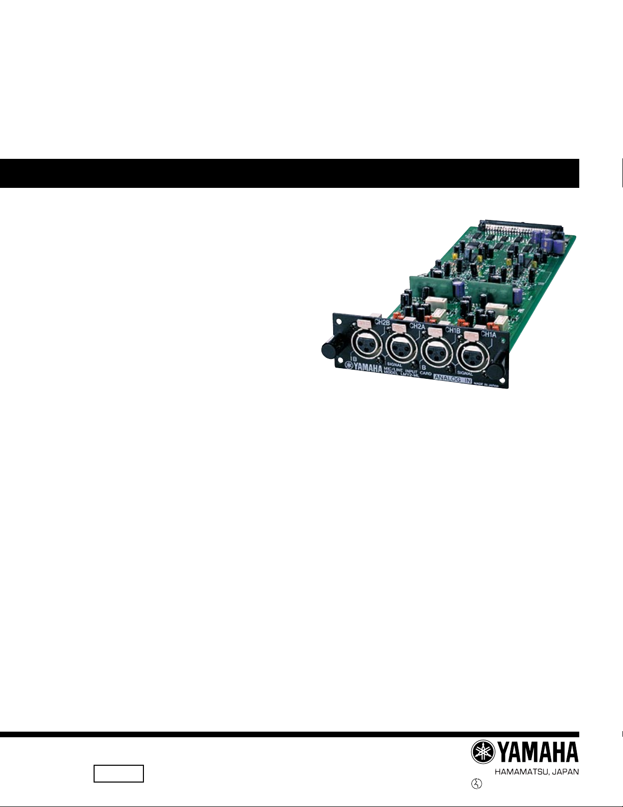
MIC/LINE INPUT CARD
LMY2-ML
SERVICE MANUAL
011502
PA
200004**-32000
■CONTENTS
SPECIFICATIONS..................................................................... 2
PANEL LAYOUT ........................................................................ 3
DIMENSIONS ........................................................................... 3
BLOCK DIAGRAM .................................................................... 4
LEVEL DIAGRAM ..................................................................... 4
LSI PIN DESCRIPTION ............................................................ 6
IC BLOCK DIAGRAM................................................................8
CIRCUIT BOARD...................................................................... 9
PARTS LIST
1.97K-9636 0.27K-9551 Printed in Japan '00.3
LMY2-ML
IMPORTANT NOTICE
This manual has been provided for the use of authorized Yamaha Retailers and their service personnel. It has been assumed that
basic service procedures inherent to the industry, and more specifically Yamaha Products, are already known and understood by the
users, and have therefore not been restated.
WARNING: Failure to follow appropriate service and safety procedures when servicing this product may result in personal injury,
destruction of expensive components, and failure of the product to perform as specified. For these reasons, we
advise all Yamaha product owners that all service required should be performed by an authorized Yamaha Retailer
or the appointed service representative.
IMPORTANT: The presentation or sale of this manual to any individual or firm does not constitute authorization, certification or
recognition of any applicable technical capabilities, or establish a principle-agent relationship of any form.
The data provided is believed to be accurate and applicable to the unit(s) indicated on the cover. The research, engineering, and
service departments of Yamaha are continually striving to improve Yamaha products. Modifications are, therefore, inevitable and
changes in specification are subject to change without notice or obligation to retrofit. Should any discrepancy appear to exist, please
contact the distributor's Service Division.
WARNING: Static discharges can destroy expensive components. Discharge any static electricity your body may have
accumulated by grounding yourself to the ground bus in the unit (heavy gauge black wires connect to this bus).
IMPORTANT: Turn the unit OFF during disassembly and part replacement. Recheck all work before you apply power to the unit.
WARNING: CHEMICAL CONTENT NOTICE!
The solder used in the production of this product contains LEAD. In addition, other electrical/electronic and /or plastic (where applicable)
components may also contain traces of chemicals found by the California Health and Welfare Agency (and possibly other entities) to
cause cancer and/or birth defects or other reproductive harm.
DO NOT PLACE SOLDER, ELECTRICAL/ELECTRONIC OR PLASTIC COMPONENTS IN YOUR MOUTH FOR ANY REASON WHATSOEVER!
Avoid prolonged, unprotected contact between solder and your skin! When soldering, do not inhale solder fumes or expose eyes to
solder/flux vapor!
If you come in contact with solder or components located inside the enclosure of this product, wash your hands before handling food.
SPECIFICATIONS
Input
Terminals
CH1A, CH1B
CH2A, CH2B
GAIN
-68 dB
+10 dB
Actual Load
Impedance
3k ohm
* 0 dB is referenced to 0.775 Vrns.
** 1=GND, 2=HOT, 3=COLD
For Use With
Nominal
50-600 ohm Mice
& 600 ohm Lines
Nominal
-68 dB (309 µV)*
+10 dB (2.45 V)*
Input Level
Maximum. Before Clip
-54 dB (1.55 mV)*
+24 dB (12.3 V)*
Connector
XLR-3-31 type
(Balanced)**
2
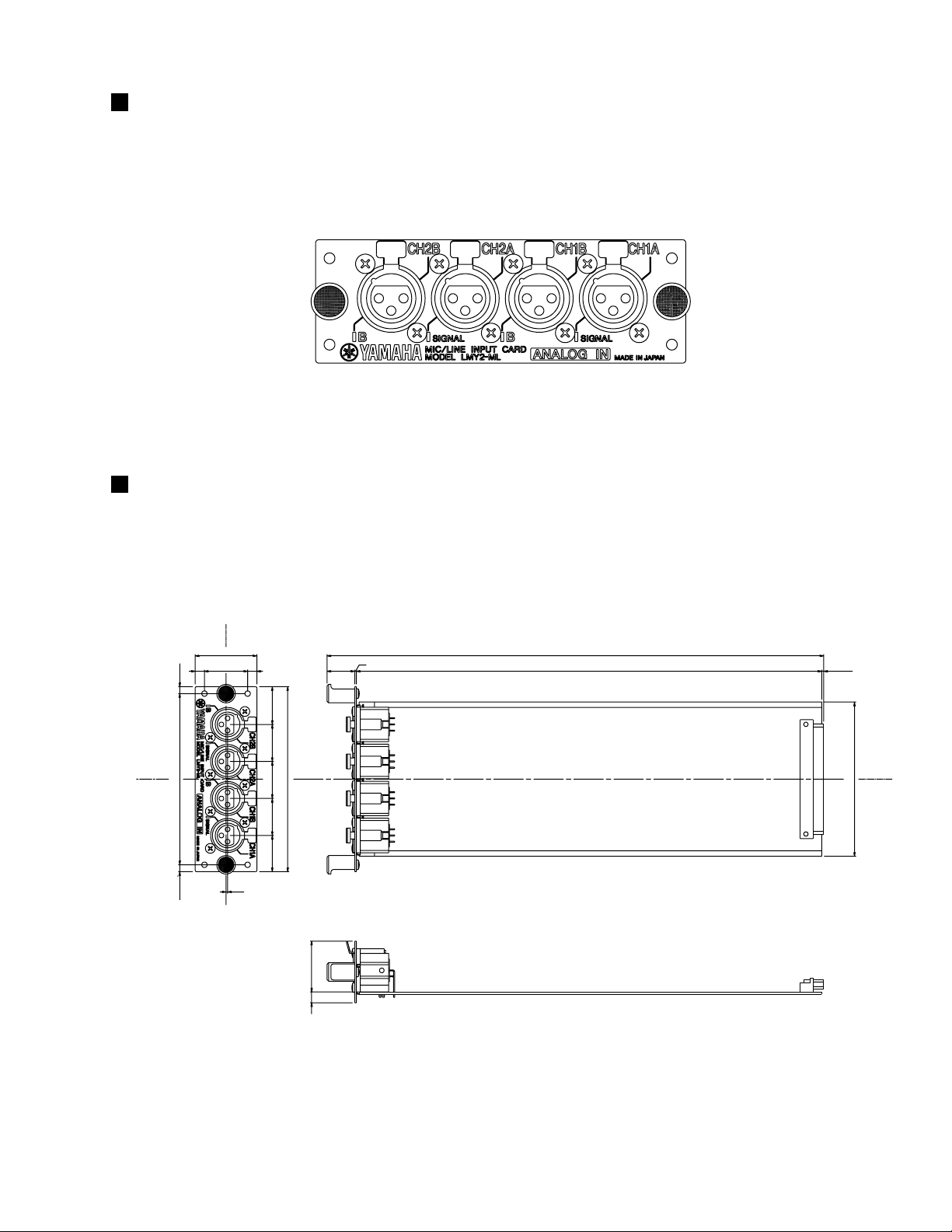
PANEL LAYOUT
DIMENSIONS
LMY2-ML
40
66
28
4.5111
(4.5)
1
24.524
24
24
(23.5)
120
1
18
33
7
322.1
301.8
(1.3)
100
Unit: mm
3
4
LMY2-ML
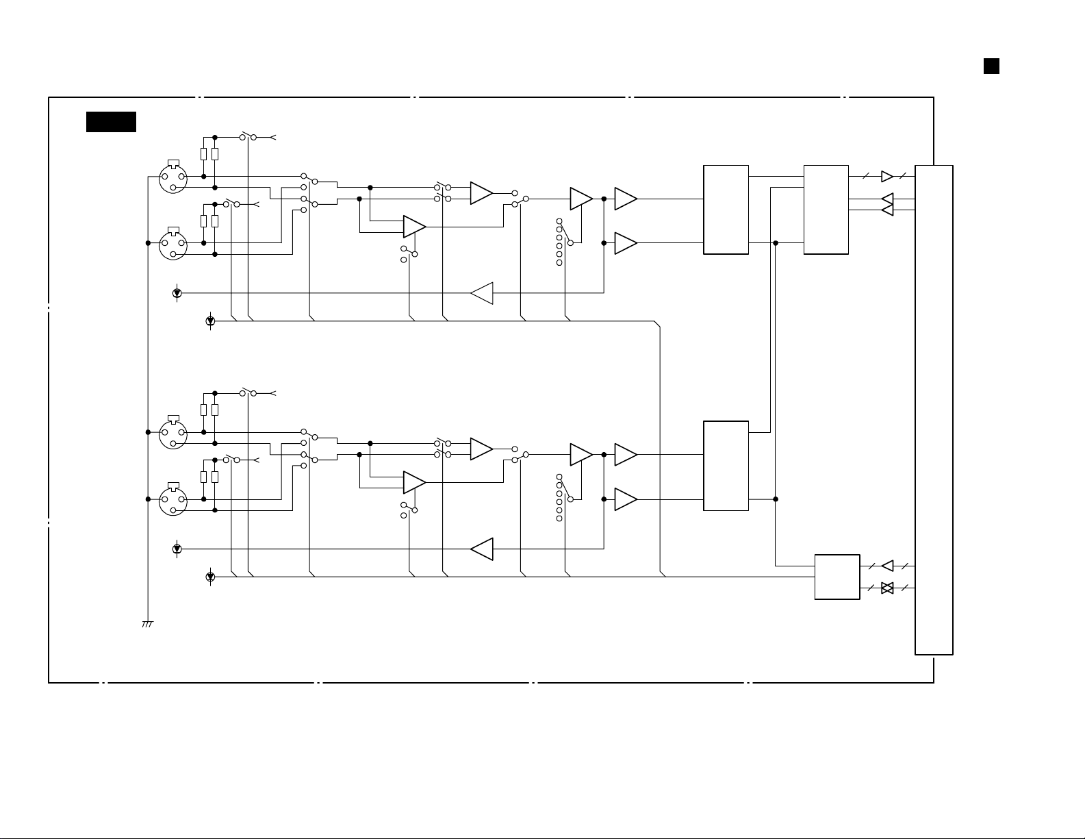
BLOCK DIAGRAM
AD1
[CH1A]
[CH1B]
[CH2A]
[CH2B]
1
GND
2
1
3
2
3
SIGNAL
2
1
3
2
1
3
SIGNAL
B
B
48V
48V
48V
48V
14dB
-4dB
14dB
-4dB
IC104
6
HA2
5
IC204
2
HA2
3
IC501
2
2
13
IC101
2
1
HA1
3
44dB
7
IC600
2
1
Amp
3
IC201
2
1
HA1
3
44dB
1
IC700
2
1
Amp
3
30dB
24dB
18dB
12dB
6dB
0dB
30dB
24dB
18dB
12dB
6dB
0dB
2
HA3
3
IC203
2
HA3
3
IC300IC103
2
1
1
Amp
3
IC300
6
Amp
5
IC400
2
Amp
3
IC400
6
Amp
5
1
7
1
7
4,5
24, 25 10
24, 25
4, 5
15
A/D
IC302
15
A/D
IC402
10
1
3
33
/RES
31
29
24
ADFC
IC500
IC505, 506, 507
5
Reg.
16 4
18 2
3
11-13
8
IC502
IC503
7
I1 a/7
SYNCM
b/15
256FS
a/19
3
A8 b/31
A9 c/32
1-3
A10 b/32
8
D00 a/34
D01 b/34
2-911-18
D02 a/35
D03 b/35
D04 a/36
D05 b/36
D06 a/37
D07 b/37
KEC-92517
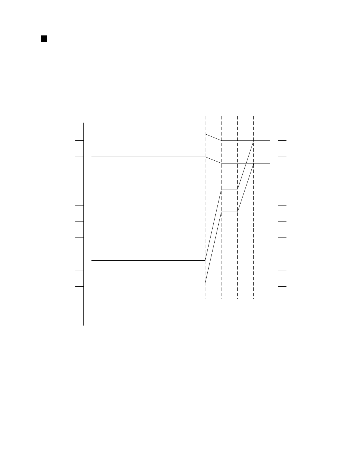
LEVEL DIAGRAM
LMY2-ML
ANALOG
dBu
+24
+20
+10
0
-10
-20
-30
-40
-50
-60
-70
MAX INPUT [24 dB]
GAIN MIN
NOMINAL INPUT [10 dB]
GAIN MIN
MAX INPUT [-54 dB]
GAIN MAX
NOMINAL INPUT [-68 dB]
GAIN MAX
HA
HA
2
1
HA
3
DIGITAL
dBFS
0
-10
-20
-30
-40
-50
-60
-70
-80
-90
-80
[0 dBu=0.775 Vrms]
KEC-92517
-100
-110
[0 dBFS: Full scale]
5
LMY2-ML
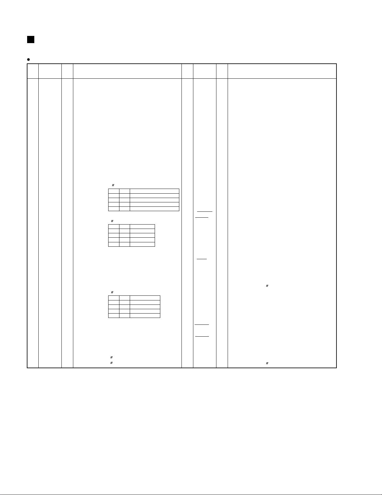
LSI PIN DISCRIPTION
YAC509 (XM167A00) ADFC
PIN
NAME I/O FUNCTION
No.
1
SI0 (L)
I
Input to Lch LO gain side (IMOD0=1)
Input to Lch (IMOD0=0)
2
3
SI1 (L)
SI0 (R)
I
Input to Lch HI gain side (IMOD0=1)
I
Input to Rch LO gain side (IMOD0=1)
Input to Rch (IMOD0=0)
4
5
6
7
IMOD0 (*)
SI1 (R)
WCKI
BCKI
I/O
I/O
I
Input to Rch HI gain side (IMOD0=1)
Word clock input/output of serial input
Bit clock input/output of serial input
I
Setting of serial input modes. "1" = parallel,
"0" = serial
8
IMOD1 (*)
I
Setting of serial input modes. "1" =
asynchronous, "0" = synchronous
9
10
11
12
13
14
ITM0 (*)
ITM1 (*)
GSEL0 (*)
GSEL1 (*)
DFC (*)
GCC (*)
I
Setting of input data timing
I
( " )
I
Setting of a floating gain
I
( " )
I
Digital filter ON/OFF ("1"=ON, "0"=OFF)
I
Automatic adjustment of floating gain
ON/OFF ("1"=ON, "0"=OFF)
15
HTC (*)
I
Quasi instantaneous cross fade bold time
ON/OFF ("1"=ON, "0"=OFF)
16
17
18
19
20
CFT0 (*)
CFT1 (*)
GND
VDD
Test1 (*)
I
Setting of cross fade time
I
( " )
GND
VDD(+5V)
I
Normally non-connected
21
22
Test2 (*)
Test3
I
O
"
"
ITM1
0
0
1
1
GSEL1
0
0
1
1
CFT1
0
0
1
1
Input timing (format)
ITM0
0
Move forward 20 bits closer
1
16 bits B.B format
0
18 bits B.B format
1
20 bits B.B format
Floating gain
GSEL0
12 dB (2 bits)
0
18 dB (3 bits)
1
24 dB (4 bits)
0
30 dB (5 bits)
1
Cross fade time
CFT0
0
1
0
1
0 ms
53 ms
106 ms
212 ms
PIN
NAME I/O FUNCTION
No.
23
XO
O
Connect X'tal OUT crystal oscillator or input
256fs clock to XI.
24
XI
I
Connect X'tal IN crystal oscillator or input
256fs clock to XI.
25
CK256A
O
Output clock which is inputted to 256fs OUT
XI.
26
27
MCK
BCKO
O
O
Output 128fs clock.
Output 64fs bit clock which divides MCK
(It rises at the head of SYNC).
28
WCKO
O
Output 1fs word clock which divides MCK
and of which the duty ratio is 50%.
29
SYNC
I/O
Input/output of 1fs synchronous clock (The
fall of SYNC makes the 6th rise of 256fs
the head of WC.)
30
31
32
SOR
SOL
CKSEL (*)
O
O
I
Output in order of Rch data and Lch data.
Output in order of Lch data and Rch data.
Switching of input or output of SYNC. "1" =
output, "0" = input.
33
34
35
RESET
MUTE (*)
OMD (*)
I
I
I
Internal reset at "0".
Output "0" for output mute all at "0".
SOL, SOR output (switching of "0"MBS
First/"1" LSB First).
36
37
38
39
40
41
NSC (*)
Test4
Test5
VDD
GND
DLSP0 (*)
I
O
O
Noise shooping ON/OFF. "1"=OFF, "0"=ON.
Normally non-connected.
"
VDD(+5V)
GND
I
Floating delay switching.
("1"=16 sample delay, "0"=0 sample delay)
42
FLSW (*)
I
Floating inhibiting SW.
"1"= floating, "0"= floating is inhibited.
ADC of output wave at HI level side.
43
44
Test6 (*)
Test7 (*)
I
I
Normally non-connected.
"
AD1: IC500
6
 Loading...