

Yamaha EMX-312-SC, EMX-512-SC Service manual
POWERED MIXER
SERVICE MANUAL
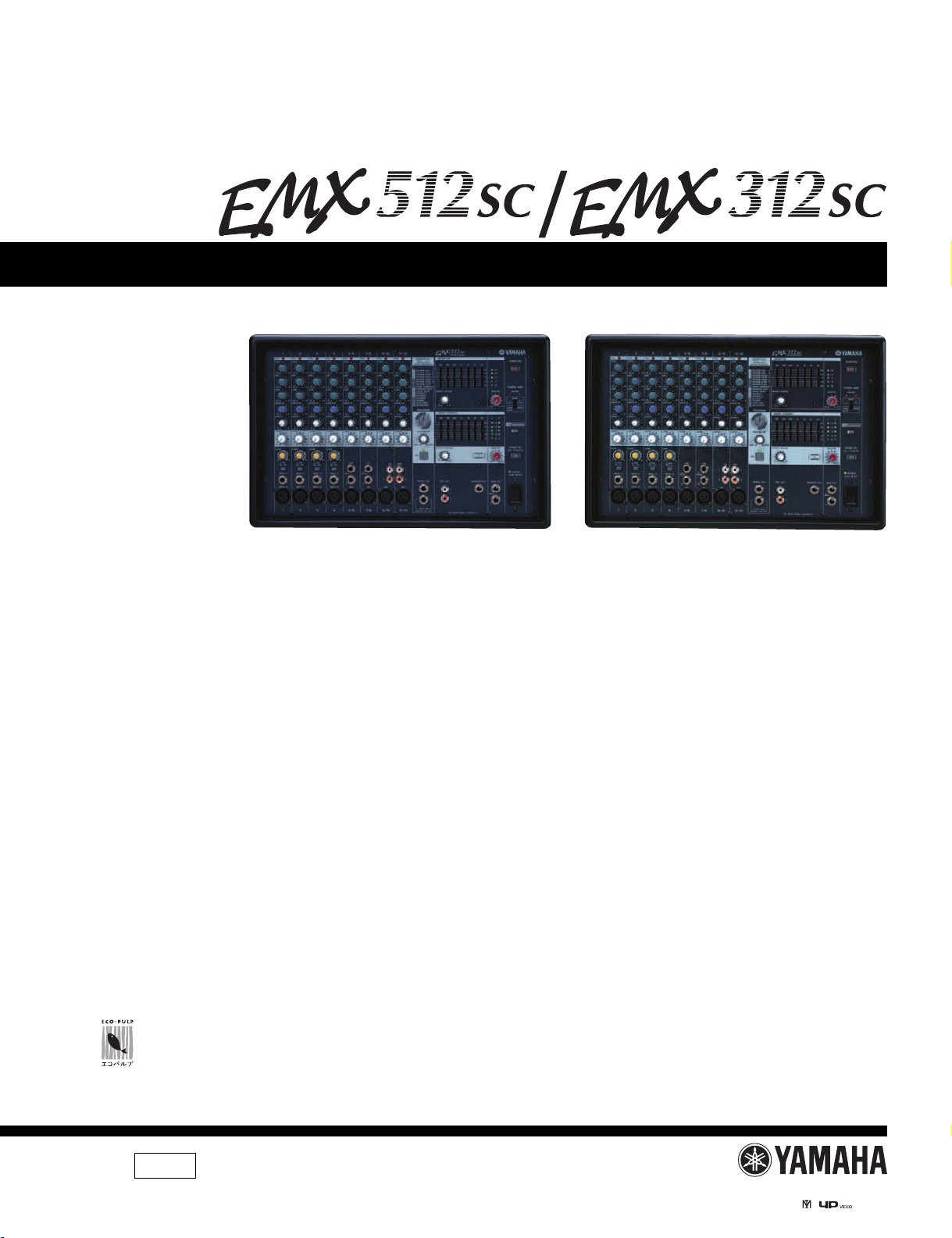
EMX512SC EMX312SC
• OPTION(別売品)
RK512 RACK MOUNT KIT (ラ ックマウン ト キッ ト)
このサービ スマニ ュア ルはエ コパルプ
(ECF : 無塩素系漂白パルプ) を使用 し ていま す。
This document is printed on chlorine free (ECF) paper.
011791
PA
EMX512SC: 200510-99750
EMX312SC: 200510-78750
RK512: 200510-5250
■ CONTENTS(目次)
SPECIFICATIONS ( 総合仕様 ) .......................................................3/5
PANEL LAYOUT ( パネルレ イアウ ト )...............................................7
CIRCUIT BOARD LAYOUT ( ユニ ッ ト レイアウ ト ) ........................10
WIRING DIAGRAM( 基板結線図 ) ....................................................11
DIMENSIONS ( 寸法図 ) ...................................................................13
DISASSEMBLY PROCEDURES ( 分解手順 ) ..................................14
LSI PIN DESCRIPTION (LSI 端子機能表 ) .......................................24
IC BLOCK DIAGRAM (IC ブロッ ク図 ) ............................................26
CIRCUIT BOARDS ( シー ト基板図 ) ................................................28
INSPECTION( 検査 ) ...................................................................50/58
PS
CIRCUIT BOARD REPAIR GUIDE
(PS シー ト 故障修理ガ イ ド )........................................................66/76
PARTS
BLOCK & LEVEL DIAGRAM( ブロッ ク & レベルダイアグラム )
CIRCUIT
LIST
DIAGRAM( 回路図 )
HAMAMATSU, JAPAN
Copyright (c) Yamaha Corporation. All rights reserved. PDF–K4902 ’05.09
EMX512SC/EMX312SC
IMPORTANT NOTICE
This manual has been provided for the use of authorized Yamaha Retailers and their service personnel. It has been assumed that basic
service procedures inherent to the industry, and more specifically Yamaha Products, are already known and understood by the users, and
have therefore not been restated.
WARNING: Failure to follow appropriate service and safety procedures when servicing this product may result in personal injury,
destruction of expensive components and failure of the product to perform as specified. For these reasons, we advise all
Yamaha product owners that all service required should be performed by an authorized Yamaha Retailer or the appointed
service representative.
IMPORTANT: This presentation or sale of this manual to any individual or firm does not constitute authorization certification, recognition
of any applicable technical capabilities, or establish a principal–agent relationship of any form.
The data provided is believed to be accurate and applicable to the unit(s) indicated on the cover. The research engineering, and service
departments of Yamaha are continually striving to improve Yamaha products. Modifications are, therefore, inevitable and changes in
specification are subject to change without notice or obligation to retrofit. Should any discrepancy appear to exist, please contact the
distributor’s Service Division.
WARNING: Static discharges can destroy expensive components. Discharge any static electricity your body may have accumulated
by grounding yourself to the ground bus in the unit (heavy gauge black wires connect to this bus).
IMPORTANT: Turn the unit OFF during disassembly and parts replacement. Recheck all work before you apply power to the unit.
WARNING: CHEMICAL CONTENT NOTICE!
The solder used in the production of this product contains LEAD. In addition, other electrical/electronic and/or plastic (Where applicable)
components may also contain traces of chemicals found by the California Health and Welfare Agency (and possibly other entities) to cause
cancer and/or birth defects or other reproductive harm.
DO NOT PLACE SOLDER, ELECTRICAL/ELECTRONIC OR PLASTIC COMPONENTS IN YOUR MOUTH FOR ANY REASON WHAT SO
EVER!
Avoid prolonged, unprotected contact between solder and your skin! When soldering, do not inhale solder fumes or expose eyes to solder/flux
vapor!
If you come in contact with solder or components located inside the enclosure of this product, wash your hands before handling food.
IMPORTANT NOTICE FOR THE UNITED KINGDOM
Connecting the Plug and Cord
IMPORTANT. GREEN-AND-YELLOW: EARTH
BLUE: NEUTRAL
BROWN: LIVE
As the colours of the wires in the mains lead of this apparatus may not correspond with the coloured markings identifying the terminals in your
plug proceed as follows:
The wire which is coloured GREEN-and-YELLOW must be connected to the terminal in the plug which is marked by the letter E or by the
safety earth symbol or colored GREEN or GREEN-and-YELLOW.
The wire which is coloured BLUE must be connected to the terminal which is marked with the letter N or coloured BLACK.
The wire which is coloured BROWN must be connected to the terminal which is marked with the letter L or coloured RED.
■ WARNING
Components having special characteristics are marked and must be replaced with parts having specification equal to those
originally installed.
印の商品は、 安全を維持する ために重要な部品です。 交換する 場合は、 安全のために必ず指定の部品 を ご使用 く ださ い。
2
EMX512SC/EMX312SC
■ SPECIFICATIONS
• General Specifications
Output RL Conditioins U, V A
Maximum Output Power SPEAKERS OUT EMX512SC 4 Ω Both ch drive, 1 kHz,
THD+N ≤ 0.5%
EMX312SC 4 Ω 300 300 300
Frequency Response CH INPUT 1-11/12 MAIN OUT, MONITOR OUT,
Maximum Voltage
Gain@ 1 kHz
Gain Error @ 1 kHz
It measures in each CH unit.
Total Harmonic Distortion
It measures in each CH unit.
(THD+N)
Hum & Noise
(20 Hz-20 kHz)
It measures in each CH unit.
EIN=Equivalent Input Noise
Residual Output Noise
(20 Hz-20 kHz)
Crosstalk @ 1 kHz
It measures in each CH unit.
Phantom Voltage
It measures in each CH unit.
CH & ST CH Equalization HIGH Turn over /roll-off frequency of
Internal Digital Effect 16 programs, Parameter control
Level Meters 2×5-points LED level meter [MAIN(L,R)], 5-points LED level meter [MONITOR] +6, +3, 0, –5, –10 [dB]
FCL Sensivity Input signal level ≥ –75dBu: LED on, CH1-4 MIC/LINE:MIC B Input, CH 5/6-11/12 MIC Input
Protection Power Amplifier POWER switch on/off mute
Input Output RL Conditioins MIN TYP MAX UNIT
EFFECT OUT, REC OUT
SPEAKERS OUT 4 Ω –3.0 0.0 1.0
CH 1-4 INPUT B,
CH 5/6-11/12 MIC
CH 1-4 INPUT B,
CH 5/6-11/12 MIC
CH 1-4 INPUT A MAIN OUT Input level: –50 dBu
CH 5/6-7/8 LINE
(Phone)
CH 9/10-11/12 LINE
(Pin)
CH INPUT 1-11/12 MAIN OUT, MONITOR OUT,
CH 1-4 INPUT B,
CH 5/6-11/12 MIC
CH INPUT 1-11/12 MAIN OUT, MONITOR OUT,
–
Input Output Conditioins MIN TYP MAX UNIT
CH 1-4 Adjacent CH inputs –65 dB
Output
CH 1-4 INPUT B,
CH 5/6-11/12 MIC
MID 2.5 k (peaking)
LOW 100 (shelving)
FOOT SW ON/OFF
Power Supply Thermal /heatsink temp ≥ 100°C :power supply shutdown /manual reset
MAIN OUT, MONITOR OUT 10 kΩ Rs=150 Ω CH1-4
MAIN OUT 10 kΩ Input level: –60 dBu
MONITOR OUT Input level: –60 dBu
EFFECT OUT Input level: –60 dBu
REC OUT Input level: –60 dBu
MAIN OUT Input level: –20 dBu 2.0 4.0 6.0
MAIN OUT Input level: –20 dBu 2.0 4.0 6.0
EFFECT OUT, REC OUT
MAIN OUT 10 kΩ EIN, Rs=150 Ω CH1-4
EFFECT OUT
MAIN OUT L, R 10 kΩ Master control at
MONITOR OUT –90
SPEAKERS OUT 4 Ω –65
MAIN OUT Input to Output
DC-fault :power supply shutdown /manual reset
Thermal /heatsink temp ≥ 90°C:output mute /auto reset
Vl limiter /RL ≤ 2 Ω
Clip limiter /THD ≥ 1 %, Indicator × 2
8 Ω 350 350 320
8 Ω 190 190 180
10 kΩ CH1-4 MIC/LINE: MIC 20
Hz-20 kHz, 0 dB @ 1 kHz
MIC/LINE:MIC
CH1-4 MIC/LINE:MIC
CH1-4 MIC/LINE:MIC
CH1-4 MIC/LINE:MIC
CH1-4 MIC/LINE:MIC
MIC/LINE:MIC
10 kΩ +14 dBu @ 20 Hz,
1 kHz, 20 kHz
MIC/LINE:MIC
Output Noise, Rs=150 Ω
CH1-4
MIC/LINE:MIC
minimum.
–
–
(LEVEL controls: minimum)
No load 14 15 16 V
shelving :3dB below maximum
variable level. ±15dB maximum
MIN 500 500 500 W
–3.0 0.0 1.0 dB
2.04.06.0dBu
2.0 4.0 6.0
–8.0 –6.0 –4.0
–12.0 –10.0 –8.0 dBV
2.04.06.0dBu
MIN TYP MAX UNIT
10 k (shelving) Hz
H, B, W, K, O
65 dB
UNIT
0.5 %
–115 dBu
–50
–90 dBu
–65
3
EMX512SC/EMX312SC
Power Consumption EMX512SC 500 W
EMX312SC 450
AC Cord Length 2450 2500 2550 mm
Dimensions Height 284 mm
Depth 264
Width 442.5
Net Weight 8kg
Included Accessories Power cord, Rubber stabilizers × 2, Owener’s Manual
Options RACK MOUNT KIT (RK512), FOOT SW (FC5)
MIN TYP MAX UNIT
Note: All level control normally: Maximum level, Output impedance of signal generator :150 Ω
• Input Characteristics
Input Terminals MIC/
CH INPUT 1-4 XLR MIC 2 kΩ 50-600 Ω Mics –60 dBu (0.775 mV) –35 dBu (13.8 mV) –15 dBu (138 mV)
Phone MIC 6 kΩ 600 Ω Lines –50 dBu (2.45 mV) –25 dBu (43.6 mV) –5 dBu (436 mV)
CH INPUT 5/6, 7/8
CH INPUT 9/10,11/12
XLR
Phone
XLR
Pin
*10 dBu is referenced to 0.775 Vrms.
2
*
Sensitivity is the lowest level that will produce an output of +4 dB (1.23 V), or the nominal output level when the unit is set to maximum level.
(All level controls are at maximum position.)
3
*
XLR-3-31 type connectors are balanced. (1=GND, 2=HOT, 3=COLD)
4
*
Phone Jacks are balanced. (Tip=HOT, Ring=COLD, Sleeve=GND)
5
*
Phone Jacks are unbalanced.
Actual
LINE
Load
Impedance
LINE –30 dBu (24.5 mV) –5 dBu (436 mV) +15 dBu (4.36 V)
LINE –20 dBu (77.5 mV) +5 dBu (1.38 V) +25 dBu (13.8 V)
2 kΩ 50-600 Ω Mics –60 dBu (0.775 mV) –35 dBu (13.8 mV) –15 dBu (138 mV)
–
10 kΩ 600 Ω Lines –20 dBu (77.5 mV) +5 dBu (1.38 V) +25 dBu (13.8 V)
–
2 kΩ 50-600 Ω Mics –60 dBu (0.775 mV) –35 dBu (13.8 mV) –15 dBu (138 mV)
–
10 kΩ 600 Ω Lines –20 dBu (77.5 mV) +5 dBu (1.38 V) +25 dBu (13.8 V)
–
For Use with
Normal
Input Level Connector
Sensitivity *
2
Nominal ( ▼ position)
Max. before Clip
XLR-3-31 type *
Phone Jack *
XLR-3-31 type *
Phone Jack *
XLR-3-31 type *
RCA Pin Jack
3
4
3
5
3
• Output Characteristics
Output Terminals Actual Source
SPEAKERS
[A1, A2, B1, B2]
MAIN OUT [L, R] 600 Ω 10 kΩ Lines
EFFECT OUT 600 Ω 10 kΩ Lines
MONITOR OUT 600 Ω 10 kΩ Lines
REC OUT [L, R] 600 Ω 10 kΩ Lines
Impedance
0.1 Ω 4 Ω Speakers EMX512SC 125 W 500 W [A1, B1] SPEAKON
*10 dBu is referenced to 0.775 Vrms. 0dBV is referenced to 1 Vrms.
2
*
Phone Jacks are unbalanced.
For Use with
Normal
Output Level Connector
Norminal Max. before Clip
+4 dBu (1.23 V) +20 dBu (7.75 V) Phone Jack*
–
+4 dBu (1.23 V) +20 dBu (7.75 V) Phone Jack*
–
+4 dBu (1.23 V) +20 dBu (7.75 V) Phone Jack*
–
–10 dBu (316 mV) +10 dBu (3.16 V) RCA Pin Jack
–
[A2, B2] Phone JackEMX312SC 75 W 300 W
2
2
2
4
■ 仕様
• 一般仕様
EMX512SC/EMX312SC
出力
最大出力
周波数特性
最大電圧ゲ イ ン @1kHz
ゲインエラー @ 1 kHz
チ ャ ンネル単位 で測定
全高調波歪率
チ ャ ンネル単位 で測定
(THD+N)
ハム & ノイズ
(20 Hz-20 kHz)
チ ャ ンネル単位 で測定
入力換算 ノ イズ
残留 ノ イズ
(20 Hz-20 kHz)
クロストーク @ 1 kHz
チ ャ ンネル単位 で測定
ファンタム電源
チ ャ ンネル単位 で測定
モノラル、 ステレオチャン
ネルイ コラ イ ザー
内蔵デジ タ ルエ フ ェ ク ト 16 プログラム、 PARAMETER コント ロール
レベルメーター 2× 5 ポイン ト LED レベルメーター [MAIN(L,R)],5 ポイン ト LED レベルメーター [MONITOR]+6,+3,0, - 5,- 10[dB]
FCL 入力感度 入力信号レベル≧- 75dBu : LED 点灯, CH1-4 MIC/LINE:MIC 入力 B, CH 5/6-11/12 入力 MIC
保護回路 パワー ア ン プ POWER スイ ッチ On/Off ミュート
SPEAKERS OUT EMX512SC 4 Ω
EMX312SC 4 Ω 300
入力 出力
CH INPUT 1-11/12 MAIN OUT, MONITOR OUT,
CH 1-4 INPUT B,
CH 5/6-11/12 MIC
CH 1-4 INPUT B,
CH 5/6-11/12 MIC
CH 1-4 INPUT A MAIN OUT Input level: –50 dBu
CH 5/6-7/8 LINE
(Phone)
CH 9/10-11/12 LINE
(Pin)
CH INPUT 1-11/12 MAIN OUT, MONITOR OUT,
CH 1-4 INPUT B,
CH 5/6-11/12 MIC
CH INPUT 1-11/12 MAIN OUT, MONITOR OUT,
–
入力 出力 条件 最小 標準 最大 単位
CH 1-4
出力
CH 1-4 INPUT B,
CH 5/6-11/12 MIC
HIGH
MID
LOW
フットスイッチ
電源 温度 / ヒ ー ト シン ク温度≧ 100 ℃ : 電源シ ャ ッ ト ダウン / 自動復帰な し
EFFECT OUT, REC OUT
SPEAKERS OUT 4 Ω –3.0 0.0 1.0
MAIN OUT, MONITOR OUT 10 kΩ Rs=150 Ω CH1-4
MAIN OUT 10 kΩ Input level: –60 dBu
MONITOR OUT Input level: –60 dBu
EFFECT OUT Input level: –60 dBu
REC OUT Input level: –60 dBu
MAIN OUT Input level: –20 dBu 2.0 4.0 6.0
MAIN OUT Input level: –20 dBu 2.0 4.0 6.0
EFFECT OUT, REC OUT
MAIN OUT 10 kΩ
EFFECT OUT
MAIN OUT L, R 10 kΩ
MONITOR OUT –90
SPEAKERS OUT 4 Ω –65
入力チ ャン ネ ル間
MAIN OUT
–
–
DC 検知 : 電源シ ャ ッ ト ダウン / 自動復帰な し
温度 / ヒ ー ト シン ク温度≧ 90 ℃ : 出力 ミ ュー ト / 自動復帰
Vl リミッター/RL ≦ 2 Ω
Clip リミッター/THD ≧ 1 % , インジケーター× 2
RL
条件 最小 標準 最大 単位
A/B 両チ ャンネル駆動 ,
8 Ω 370
1kHz, THD+N ≦ 0.5%
8 Ω 190
RL
条件 最小 標準 最大 単位
10 kΩ CH1-4 MIC/LINE: MIC 20
Hz-20 kHz, 0 dB @ 1 kHz
MIC/LINE:MIC
CH1-4 MIC/LINE:MIC
CH1-4 MIC/LINE:MIC
CH1-4 MIC/LINE:MIC
CH1-4 MIC/LINE:MIC
MIC/LINE:MIC
10 kΩ +14 dBu @ 20 Hz,
1 kHz, 20 kHz
入力換算 ノ イズ ,
Rs=150 Ω CH1-4
MIC/LINE:MIC
Output Noize, Rs=150 Ω
CH1-4
MIC/LINE:MIC
Master コントロール=
最小レ ベル
LEVEL コント ロール= 最小レベル
負荷な し
シェルビングタ イプのターンオー
バー / ロ ールオ フ 周波数 : 最大可
幅に対し て 3 dB 下がっ たポイ ン
± 15dB ( 最大可変幅 )
500 W
–3.0 0.0 1.0 dB
2.04.06.0dBu
2.0 4.0 6.0
–8.0 –6.0 –4.0
–12.0 –10.0 –8.0 dBV
2.04.06.0dBu
最小 標準 最大 単位
14 15 16 V
10 k (
シェルビングタイプ)
2.5 k (
ピーキングタ イプ)
100 (
シェルビングタイプ)
ON/OFF
65 dB
0.5 %
–115 dBu
–50
–90 dBu
–65 dB
–65
Hz
5
EMX512SC/EMX312SC
消費電力
電源コ ー ド 長 さ
最大外形寸法 高さ
質量
付属品 電源コ ー ド、 ス ピー カ ーケー ブル× 2、ゴム製スタビライザー× 2、 取扱説明書
オプシ ョ ン ラ ックマウン ト キッ ト (RK512)、フットスイッチ(FC5)
EMX512SC 500 W
EMX312SC 450
奥行
幅
Note: LEVEL コントロール= 最大レ ベル、 出力イ ンピ ー ダ ン ス = 150Ω
• 入力仕様
入力端子名称
CH INPUT 1-4 XLR MIC 2 kΩ 50-600 Ω
Phone MIC 6 kΩ
CH INPUT 5/6, 7/8
CH INPUT 9/10, 11/12
*10 dBu = 0.775 Vrms.
2
入力感度 : 最大ゲイ ン 測定時に + 4 dB(1.23 V) または定格出力が得 ら れ る 最小レ ベル
*
3
*
バランス型XLR-3-31 タイプ端子 (1 =グ ラ ウ ン ド、 2 =ホ ッ ト、 3 =コールド)
4
*
バランス型フォーン端子 (T =ホッ ト 、 R =コールド、 S =グラウン ド)
5
*
アンバランス型フォーン端子
XLR
Phone
XLR
Pin
MIC/
入力イ ン
LINE
ピーダンス
LINE –30 dBu (24.5 mV) –5 dBu (436 mV) +15 dBu (4.36 V)
LINE –20 dBu (77.5 mV) +5 dBu (1.38 V) +25 dBu (13.8 V)
2 kΩ 50-600 Ω
–
10 kΩ
–
2 kΩ 50-600 Ω
–
10 kΩ
–
適合イ ンピ ー
ダンス
マイク
600 Ω ライン
マイク
600 Ω ライン
マイク
600 Ω ライン
入力レ ベル 端子仕様
2
感度 *
–60 dBu (0.775 mV) –35 dBu (13.8 mV) –15 dBu (138 mV)
–50 dBu (2.45 mV) –25 dBu (43.6 mV) –5 dBu (436 mV)
–60 dBu (0.775 mV) –35 dBu (13.8 mV) –15 dBu (138 mV)
–20 dBu (77.5 mV) +5 dBu (1.38 V) +25 dBu (13.8 V)
–60 dBu (0.775 mV) –35 dBu (13.8 mV) –15 dBu (138 mV)
–20 dBu (77.5 mV) +5 dBu (1.38 V) +25 dBu (13.8 V)
ノミナルレベル
(▼の位置)
最小 標準 最大 単位
2450 2500 2550 mm
284 mm
264
442.5
8kg
最大 ノ ン ク リ ッ プ
レベル
XLR-3-31
フォーン端子
XLR-3-31
フォーン端子
XLR-3-31
RCA
タイプ
*
*
タイプ
*
タイプ
ピン端子
3
4
*
*
3
5
3
• 出力仕様
出力端子名称 出力イ ンピ ー
SPEAKERS
[A1, A2, B1, B2]
MAIN OUT [L, R] 600 Ω
EFFECT OUT 600 Ω
MONITOR OUT 600 Ω
REC OUT [L, R] 600 Ω
*10 dBu = 0.775 Vrms、 0dBV=1Vrms とする
2
*
アンバランス型フォーン端子
ダンス
0.1 Ω 4 Ω Speakers EMX512SC 125 W 500 W
適合イ ンピ ー
ダンス
10 kΩ ライン
10 kΩ ライン
10 kΩ ライン
10 kΩ ライン
出力レ ベル 端子仕様
ノミナルレベル 最大 ノ ン ク リ ッ プ
EMX312SC 75 W 300 W
+4 dBu (1.23 V) +20 dBu (7.75 V)
–
+4 dBu (1.23 V) +20 dBu (7.75 V)
–
+4 dBu (1.23 V) +20 dBu (7.75 V)
–
–10 dBu (316 mV) +10 dBu (3.16 V)
–
レベル
[A1, B1] スピコン端子
[A2, B2] フォーン端子
フォーン端子*
フォーン端子*
フォーン端子*
RCA ピン端子
2
2
2
6
■ PANEL LAYOUT(パネルレイアウト)
EMX512SC/EMX312SC
• Controls on Each channel
(各チャンネルコントロール)
1
1
2
3
4
5
3
4
5
6
1
3
4
5
•
Digital Effect Section
0
q
w
(デジタルエフェクト部)
7
9
8
1 FCL (Feedback Channel Locating) indicator
2 Equalizer gain control (HIGH, MID, and LOW)
3 MONITOR control
4 EFFECT control
5 LEVEL control
6 COMP control
7 LINE/MIC switch (Channels 1 to 4)
8 INPUT A and INPUT B jacks (Channels 1 to 4)
9 LINE and MIC jacks (Channels 5/6 to 11/12)
1 FCL (フ ィードバッ クチャンネルロケーテ ィ ング)
2 EQ ゲインコン ト ロール (HIGH、 MID、 LOW)
3 MONITOR コン ト ロール
4 EFFECT コント ロール
5 LEVEL コン ト ロール
6 COMP コン ト ロール
7 LINE/MIC スイッチ
8 INPUT A/B 端子 (チ ャ ンネル 1 から 4)
9 LINE/MIC 端子 (チ ャ ンネル 5/6 から 11/12)
e
r
0 PROGRAM selector
q PARAMETER control
w DIGITAL EFFECT ON switch
e EFFECT OUT jack
r FOOT SW jack
0 PROGRAM セレクター
q PARAMETER コント ロール
w DIGITAL EFFECT ON スイッチインジケーター
e EFFECT OUT 端子
r FOOT SW 端子
7
EMX512SC/EMX312SC
• MAIN Section(MAIN 部)
t
y
i
u
• MONITOR Section(MONITOR 部)
a
s
f
d
t Graphic Equalizer faders
y EFFECT RETURN control
u MASTER control
i LEVEL meters
o MAIN OUT L and R jacks
p REC OUT L and R jacks
t GEQ (グラ フ ィ ッ クイ コ ラ イザー) フ ェーダー
y EFFECT RETURN コント ロール
u MASTER コン ト ロール
i LEVEL メーター
o MAIN OUT L/R 端子
p REC OUT L/R 端子
op
g
a Graphic Equalizer faders
s EFFECT RETURN control
d MASTER control
f LEVEL meters
g MONITOR OUT jack
a GEQ (グラ フ ィ ッ ク イ コ ラ イザー) フ ェ ーダー
s EFFECT RETURN コント ロール
d MASTER コントロール
f LEVEL メーター
g MONITOR OUT 端子
8
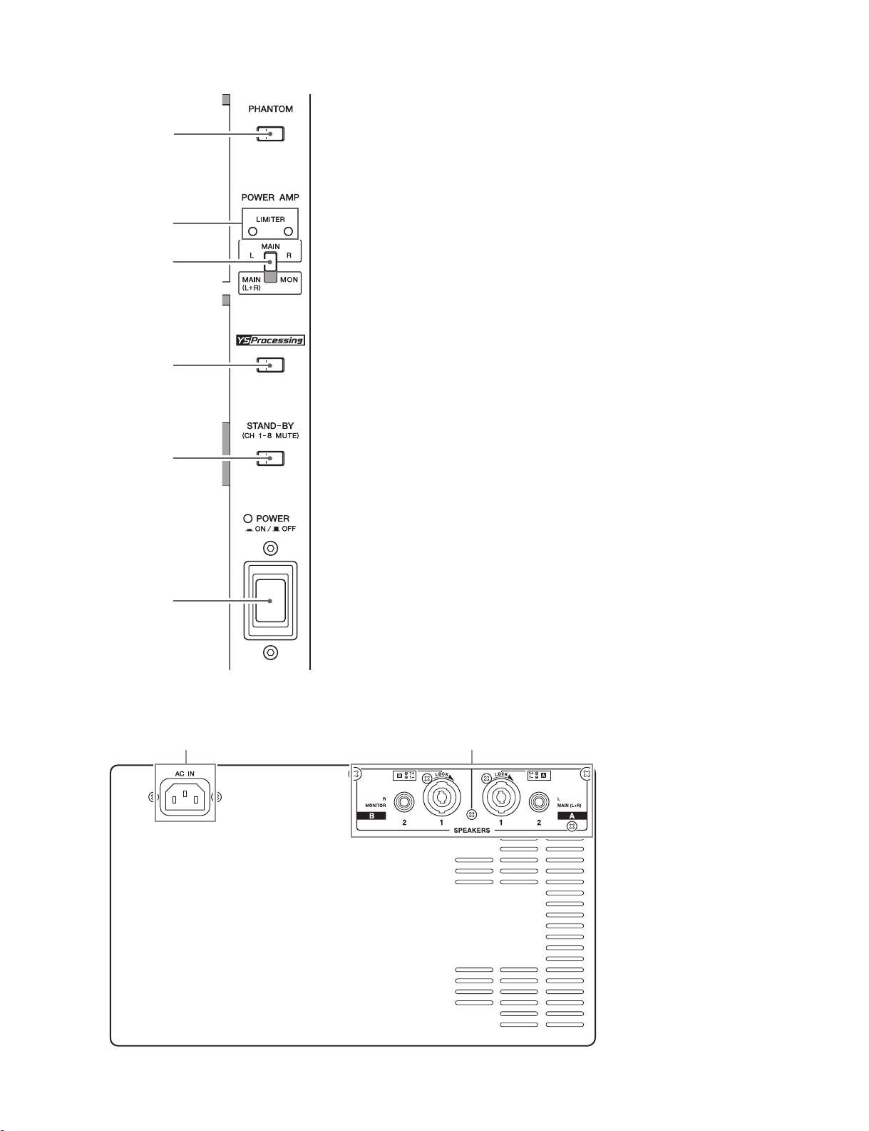
• POWER Section(POWER 部)
h
EMX512SC/EMX312SC
h PHANTOM switch
j LIMITER indicators
k POWER AMP switch
l YS Processing switch
; STAND-BY switch
z POWER switch and indicator
j
k
l
;
z
h PHANTOM スイッチ
j LIMITER インジケーター
k POWER AMP 切り替えスイッチ
l YS Processing スイッチ
; STAND-BY スイッチ
z POWER スイッチ、 インジケーター
• Rear panel(リアパネル)
xc
x SPEAKERS jacks
c AC IN connector
x SPEAKERS 端子
c AC IN 端子
9
EMX512SC/EMX312SC
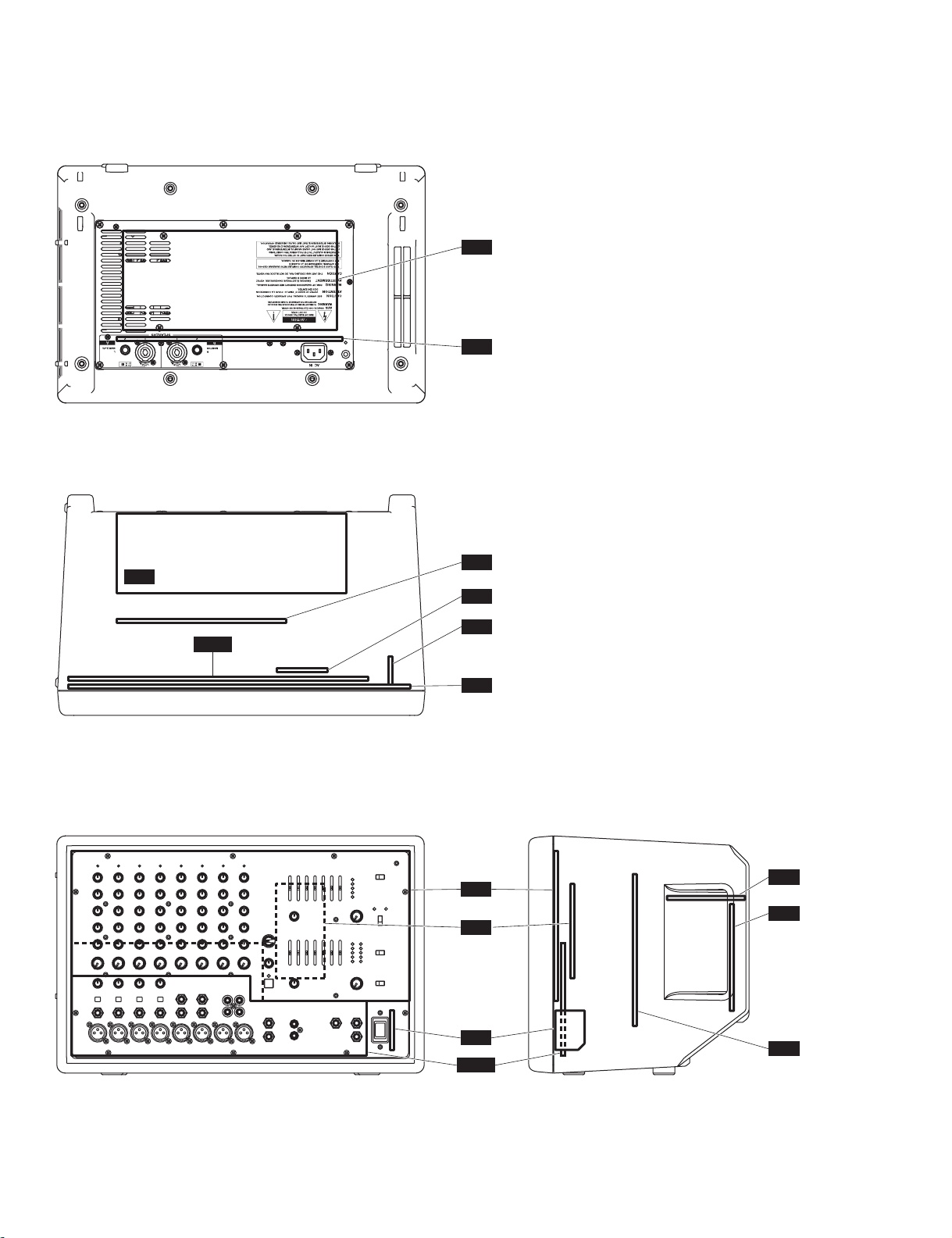
■ CIRCUIT BOARD LAYOUT(ユニットレイアウト)
• Rear View(背面図)
PA
OUT
• Top View(上面図)
OUT
PS
DSP
SW
JACK
MIX
• Front View(正面図) • Side View(側面図)
MIX
DSP
OUT
PA
10
SW
JACK
PS
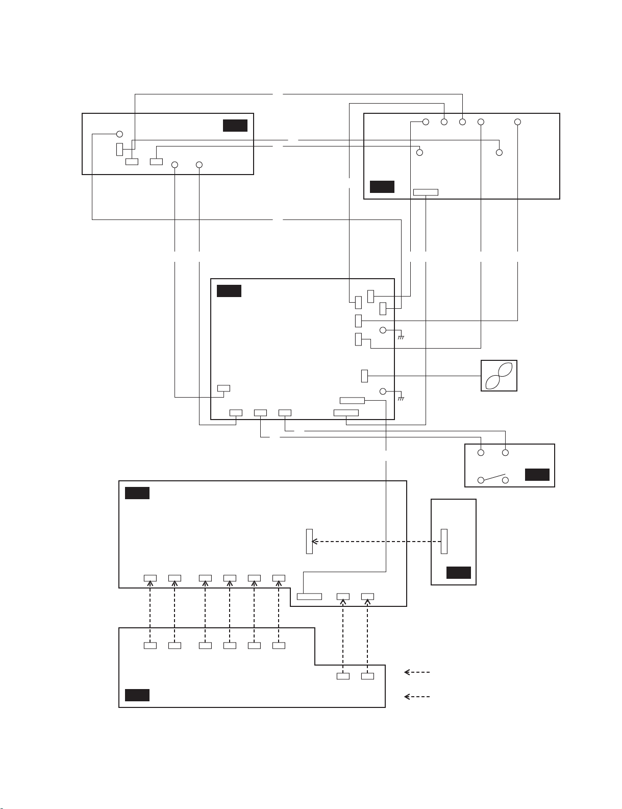
■ WIRING DIAGRAM(基板結線図)
BLACK
7
EMX512SC/EMX312SC
CN303
W305
CN301 CN302
BROWN
W304 W303
OUT
BLACK
PS
CN402
CN401 CN410 CN411
GRAY
2
8
w
VIOLET
1
YELLOW
q
CN405
CN415
(14P)
*
3
RED
CN409
CN408
CN404
CN416(13P)
GRAY
CN406
PA
ORANGE
CN407
r
W106
CN101(14P)
4 e 5 69 0
W401
W402
W104 W103
YELLOW
W107 W105
W102W101
BLUE WHITE
FAN
W602
W601
*
SW
MIX
CN002
CN001
(3P)
(3P)
CN002
CN001
(3P)
(3P)
JACK
* EMX512SC only
EMX512SCのみ
CN101
(3P)
CN101
(3P)
CN102
(3P)
CN102
(3P)
CN201
(3P)
CN201
(3P)
CN202
(3P)
CN202
(3P)
CN301(20P)
CN401
(13P)
CN302
(5P)
CN402
(5P)
CN402
(7P)
CN401
(7P)
CNM02(20P)
DSP
indicates that connectors are connected
directly to circuit boards.
はコネクターが直接基板に接続されて
いることを表しています。
11
EMX512SC/EMX312SC
No. Part No. Assembly Name Connection Remarks
線材名 接続 備考
(WE29820) Connector Assembly B&C
1
(WE29900) Connector Assembly B&C
2
(WE29840) Connector Assembly B&C
3
(WE29850) Connector Assembly B&C
4
(WE29860) Connector Assembly B&C
5
(WE29870) Connector Assembly B&C
6
(WE29910) Connector Assembly B&C
7
(WF58250) Connector Assembly B&C
8
(WE29930) Connector Assembly B&C
9
(WE29940) Connector Assembly B&C
0
(WE29880) Connector Assembly B&C
q
(WE29940) Connector Assembly B&C
w
(WE34870) Jumper Wire SMV2J P=2 14-300
e
(WE25580) Jumper Wire SMV2J P=2 13-230
r
束線
束線
束線
束線
束線
束線
束線
束線
束線
束線
束線
束線
ジャンパーリード
ジャンパーリード
Parts in parentheses are not available as spare parts.
カ ッ コ 内の部品はサービ ス部品 と し て準備 さ れてい ません。
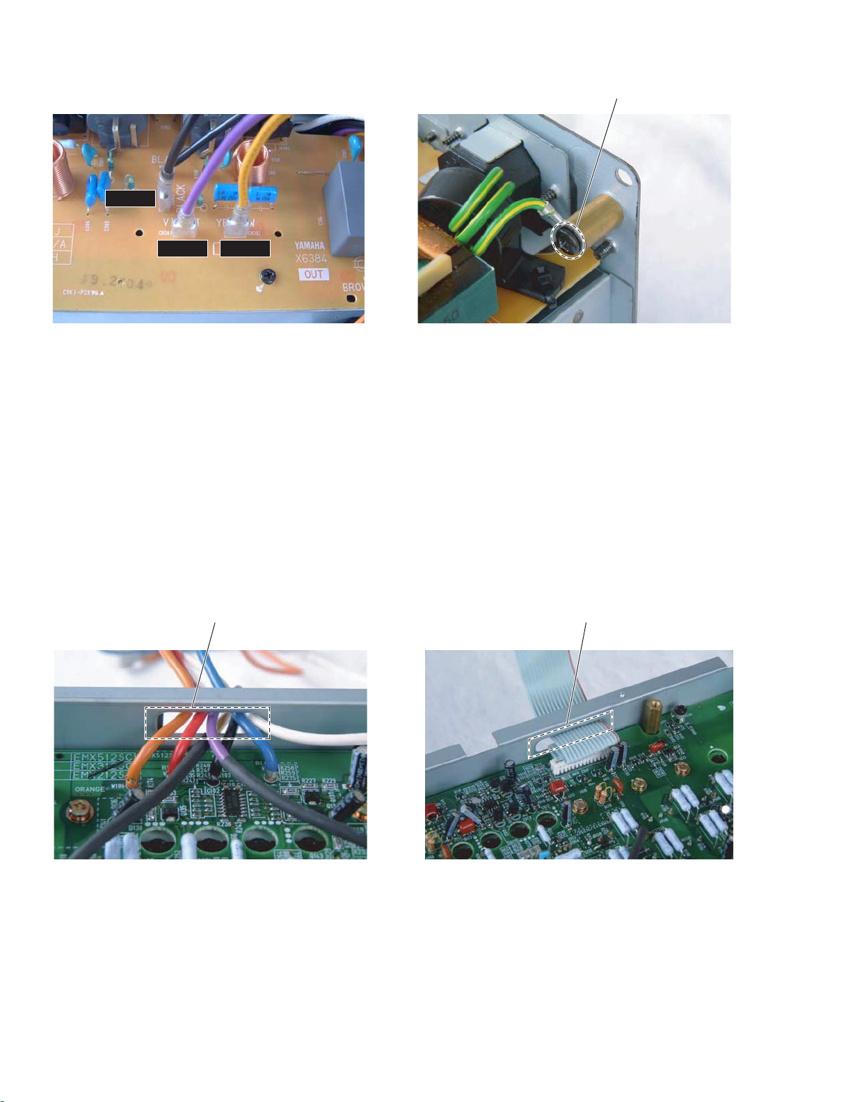
PA-W102 <-> OUT-CN301 Violet
PA-W101 <-> OUT-CN302 Yellow
PA-W104 <-> PS-CN405 Red, EMX512SC only
PA-W106 <-> PS-CN406 Orange
PA-W107 <-> PS-CN408 Blue
PA-W105 <-> PS-CN409 White, EMX512SC only
PA-W103 <-> OUT-CN303 Black
OUT-W305 <-> PS-CN406 Black
OUT-W304 <-> PS-CN402 Brown
OUT-W303 <-> PS-CN401 Gray
SW-W602 <-> PS-CN411 Yellow
SW-W601 <-> PS-CN410 Gray
PS-CN415 <-> PA-CN101
PS-CN416 <-> MIX-CN401
12
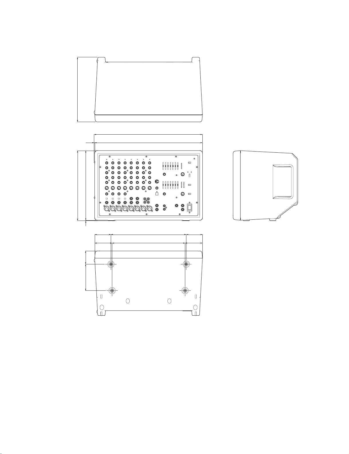
■ DIMENSIONS(寸法図)
EMX512SC/EMX312SC
442.5
4402.5
286 264
66.1
71
54108 2842
307.8
298
66.1
71
Unit: mm
単位 : mm
13
EMX512SC/EMX312SC
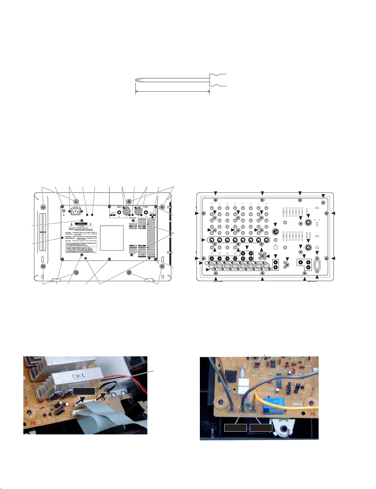
■ DISASSEMBLY PROCEDURES
•Preparing
A screwdriver with a long shaft is required to remove some
screws.
220 mm or more
1. Front Panel Unit (Time required: about 5 minutes)
1-1 Remove the eight (8) screws marked [690]. (Fig.1)
• Remove the jumper wire from CN416 on the PS circuit
board and the wires (gray and yellow) from CN410 and
CN411 on the PS circuit board. The front panel unit can
then be removed. (Photo.1 & Photo2)
* When removing the front panel only, remove the screws
and knobs marked with
[690]
▼ . (Fig.1)
[630][630] [150][130][170]
[180] [150] [180] [130]
■ 分解手順
• 準備
一部のネジの取 り 外 し には、 軸が長い ド ラ イバーが必
要です。
1. フロントパネルユニット (所要時間 : 約5 分)
1-1 [690] のネジ 8 本を外し、 フ ロン ト パネルユニッ ト を外
します。( 図1)
•PSシー トの CN416 からジャンパーリード を、 CN410、
CN411 から 束線 (灰色、 黄色) を 外す と、 フ ロ ン ト パ
ネルユニ ッ ト の分離がで き ま す。 (写真 1、写真2)
※ フ ロ ン ト パネル印刷上 り のみを取 り 外す場合は、 ▼マー ク
がついた ネジお よ び ノブ を外し ます。 (図 1)
[690]
[50]
[130]
[630]
[50]
[630]
[130]
[630][50][630]
[50]: Bind Head Screw 4x8 MFZN2B3 (WE969000) 小ネジ+ BIND
[130]: Bind Head Tapping Screw-S 3x6 MFZN2B3 (WE877800) S タイト+BIND
[150]: Bind Head Tapping Screw-S 3x6 MFZN2B3 (WE877800) S タイト+BIND
[170]: Bind Head Tapping Screw-B 3x12 MFZN2B3 (WE998100) B タイト+BIND
[180]: Flat Fillister H. Tapping 3x8 MFZN2W3 (WF790100) B タイト+平頭
[630]: Bind Head Tapping Screw-P 4x16 MFZN2B3 (WE980800) P タイト+BIND
[690]: Bind Head Tapping Screw-P 5x25 MFZN2W3 (WG158600) P タイト+BIND
[690][690]
Fig.1 (図 1)
PS circuit board (PSシート)
PS circuit board
(PS
シート)
CN416
14
CN411CN410
Photo.1 (写真 1)
Photo.2 (写真 2)

EMX512SC/EMX312SC
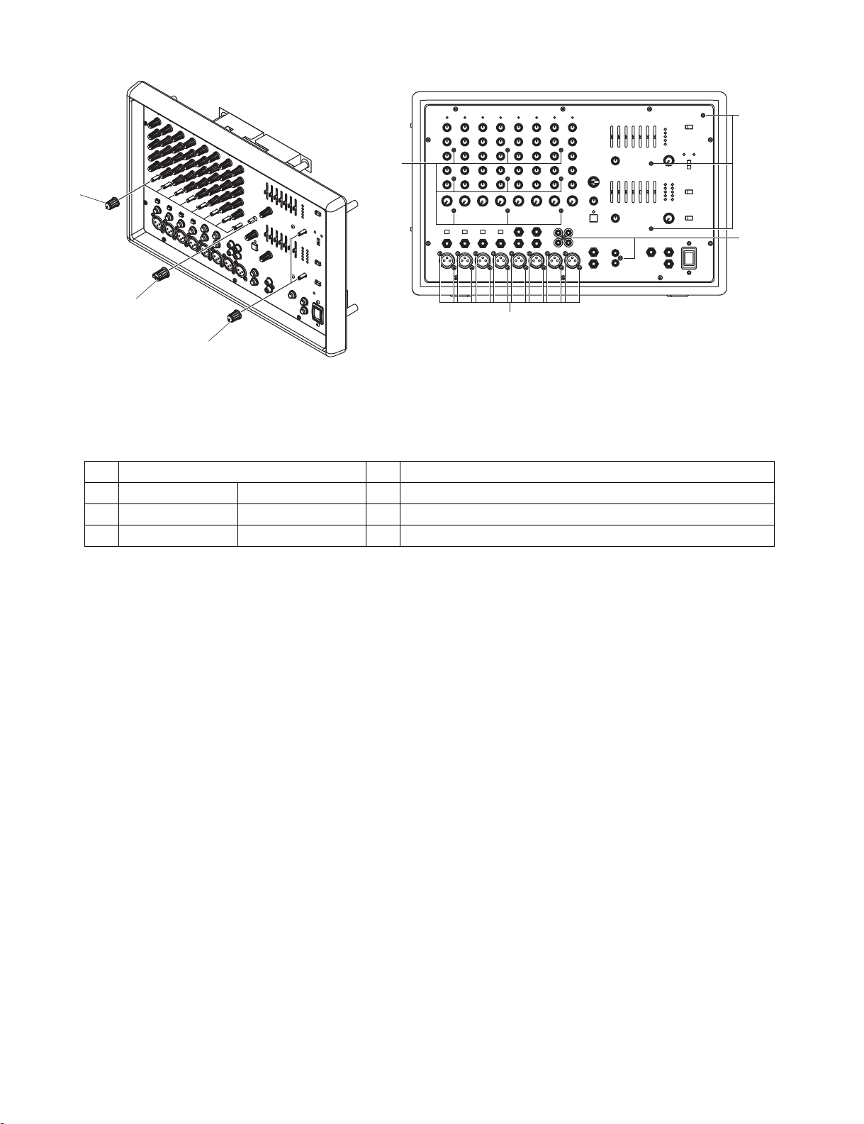
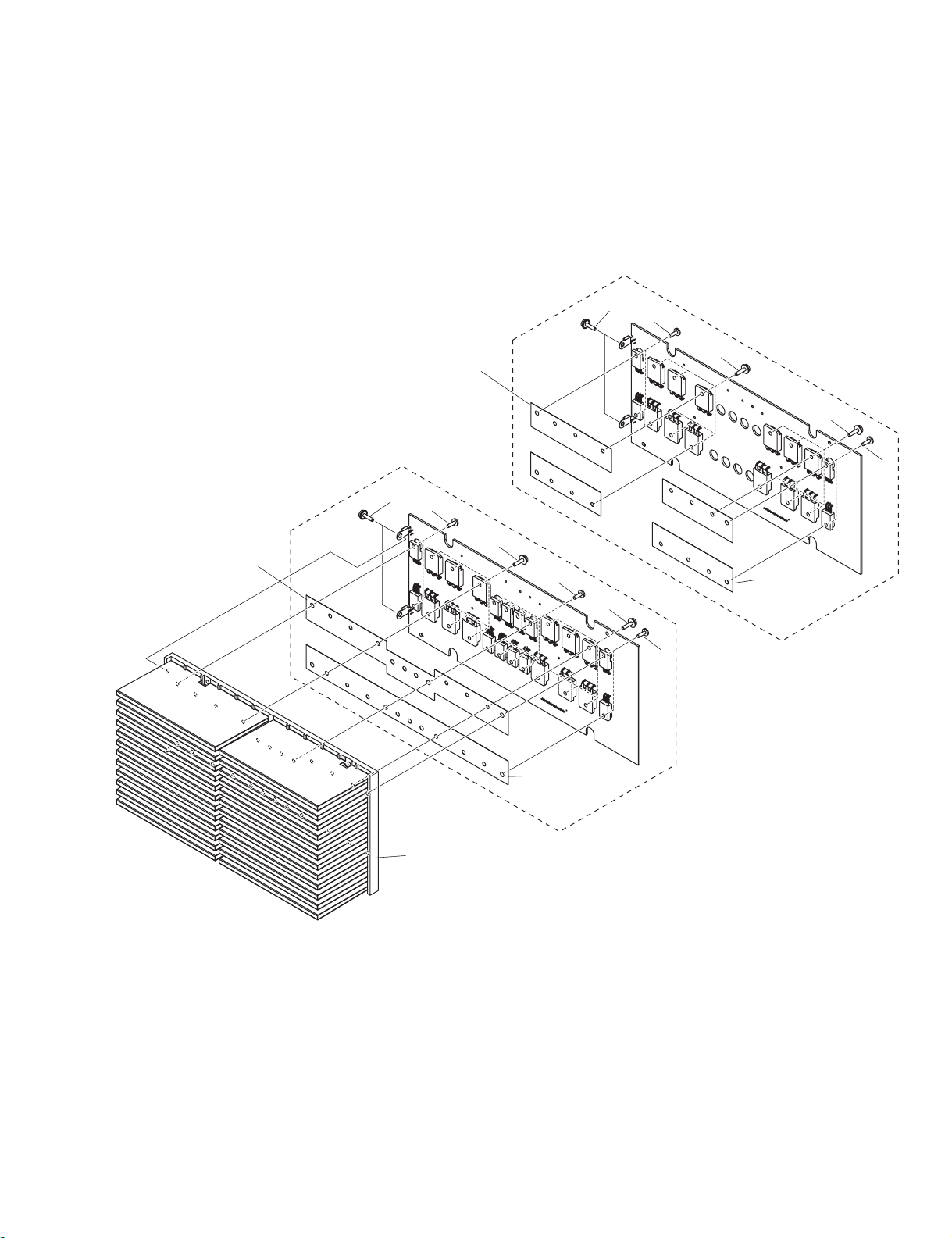
2. JACK, DSP and MIX Circuit Boards
1 Remove the front panel unit. (See procedure 1.)
2 Remove the knobs specified in the Fig.2 and Table.1.
3 Remove the eighteen (18) screws marked [500], twelve (12)
screws marked [490] and thirteen (13) hexagonal nuts and
washers. (Fig.2 & Fig.3)
4 Remove the fourteen (14) screws marked [510]. The JACK,
DSP and MIX circuit boards can then be removed together.
(Fig.3)
5 Remove the four (4) screws marked [514] and the shield
plate can then be removed. (Fig.4)
2-1 JACK Circuit Board
(Time required: about 5 minutes)
2-1-1 Remove the two (2) hexagonal spacer marked [511], the
screw marked [410] and the two (2) screws marked [430].
The JACK circuit board can then be removed. (Fig.3 &
Fig.4)
2-2 DSP Circuit Board
(Time required: about 4 minutes)
2-2-1 Remove the two (2) screws marked [470] and the cover
DSP. (Fig.3)
2-2-2 Remove the four (4) screws marked [450]. The DSP circuit
board can then be separated from the MIX circuit board.
(Fig.3)
2-3 MIX Circuit Board (Time required: about 1 minute)
2-3-1 Remove the shield. (Fig.3)
* When attaching the JACK circuit board, be sure to pass
the jumper wire from the MIX circuit board through the
slit on the JACK circuit board. (Photo.3)
* The following parts are not included in the circuit
boards. Be sure to remove them when replacing the
circuit boards. (Fig.3)
JACK: [360] Knob Black
[370] Knob Black
[610] Button D-Gray/White (LINE/MIC)
MIX: [340] Button Milky/D-Gray (PHANTOM,
YSProcessing, STAND-BY)
[390] Hexagonal Spacer
[580] Button
* When replacing [340] Button Milky/D-Gray, replace
three buttons at the save time. Also when replacing
[610] Button D-Gray/White, replace four buttons at the
same time.
2. JACK シー ト、 DSP シート 、 MIX シー ト
1 フロントパネルユニッ ト を外します。 (1 項参照)
2 図 2および表1 のノブを外します。
3 [500] のネジ18 本、[490] のネジ12 本、13 個の六角ナ ッ ト
と ワ ッ シ ャ ーを外し ます。 (図 2、図3)
4 [510] のネジ14 本を外し、JACK シート 、DSP シー ト、MIX
シー ト を外し ます。 (図3)
5 [514] のネジ 4 本を外し、 シールドプレー ト H を外し ま
す。 (図 4)
2-1 JACK シー ト (所要時間 : 約 5 分)
2-1-1 [511] の 6 角ス ペーサ 2個、 [410] のネジ 1 本、 [430] のネ
ジ 2 本を外し、 JACK シート を外し ます。 (図3、図4)
2-2 DSP シー ト (所要時間 : 約4 分)
2-2-1 [470] のネジ 2 本を外し、カバーDSP を外 し ます。(図 3)
2-2-2 [450] のネジ 4 本を外し、 MIX シー ト か ら DSP シー ト を
外します。 (図3)
2-3 MIX シー ト (所要時間 : 約 1 分)
2-3-1 シールド DSP を外 し ま す。 (図 3)
※ JACK シー ト を取り付けると きは、 MIX シー トからの束線
を JACK シー トのスリ ッ トに通して ください。 (写真3)
※ 下記の部品はシー ト 基板の構成部品ではあ りません。 シー
ト 基板 を交換す る と き は外 し て使用し て く ださ い。 (図 3)
JACK: [360] ノブ継ぎ手VRS
[370] ノブ継ぎ手HP F
[610] ボタン HP F (LINE/MIC)
MIX: [340] ボタン P F L (PHANTOM,YSProcessing,
STAND-BY)
[390] 六角ス ペーサ M 3
[580] ボタン T AP
※ [340] ボタン PFL を交換する場合は、 同時に 3 個交換する
ことをおすすめします。また[610] ボタン HPF を交換する
場合は同時に 4 個交換する こ と をおすすめ し ます。
3. Front Frame (Time required: about 10 minutes)
3-1 Remove the front panel unit. (See procedure 1.)
3-2 Remove the JACK, DSP and MIX circuit boards. (See
procedure 2.)
3-3 Remove the two (2) screws marked [300]. (Fig.3)
3-4 Remove the ten (10) screws marked [260]. The front frame
can then be separated from the front panel. (Fig.3)
3. フ ロ ン ト フ レーム (所要時間 : 約 10 分)
3-1 フロントパネルユニット を外します。 (1 項参照)
3-2 JACK シー ト 、 DSP シート 、 MIX シー ト を外し ます。 (2
項参照 )
3-3 [300] のネジ 2 本を外します。 (図3)
3-4 [260] のネジ 10 本を外すと、フロ ン ト フレーム とフ ロ ン
ト パネル印刷上 り の分離がで き ます。 ( 図3)
15
EMX512SC/EMX312SC
[560]
[600]
[490]: Hex. Socket Set Screw 3x6 MFZN2B3 (WF419300) S タイト6角孔付き
[500]: Bonding Tapping Screw-B 3x10 MFZN2B3 (WE878000) B タイト+ BOND
Table.1(表 1)
<Front panel unit>
[490]
[490]
[500]
[500]
[570]
Fig.2 (図 2)
No. Description Q’ty Control
560 Knob White/M-Gray
570 Knob Red/M-Gray
600 Knob Black
ノブ LE VE L
ノブ LE VE L
ノブ SE L E C T 色上
8 LEVEL (CH1-11/12)
2 MASTER (MONITOR, MAIN)
1 PROGRAM
16
EMX512SC/EMX312SC
[260]
[260]
Hexagonal nut & washer
(六角ナット&ワッシャー)
SW circuit board
(SW
シート)
[290]
[300]
Power switch knob
(PSW
ノブ)
Switch assembly
(
スイッチAss’y)
[360]
[610]
[390]
[370]
[390]
[510]
[510]
[390]
(
シールドDSP)
[580]
DSP circuit board
(DSP
シート)
Shield
[510]
[340]
[410]
[510]
[450]
[430]
[470]
Cover DSP
(
カバーDSP)
[260]: Bind Head Tapping Screw-P 3x10 MFZN2B3 (WF268000) P タイト+BIND
[290]: Bind Head Tapping Screw-P 3x6 MFZN2W3 (WE877900) S タイト+BIND
[300]: Hex. Socket Set Screw 3x6 MFZN2B3 (WF419300) S タイト6角孔付き
[410]: Bind Head Tapping Screw-S 3x5 MFZN2W3 (WE980200) S タイト+BIND
[430]: Bind Head Tapping Screw-P 3x6 MFZN2W3 (WE877900) S タイト+BIND
[450]: Bind Head Tapping Screw-P 3x6 MFZN2W3 (WE877900) S タイト+BIND
[470]: Bind Head Tapping Screw-S 3x5 MFZN2W3 (WE980200) S タイト+BIND
[510]: Bind Head Tapping Screw-P 3x10 MFZN2W3 (WF001000) Pタイト+BIND
Fig.3 (図 3)
Shield plate
(
シールドプレートH)
[514]
[511]
[511]: Hexagonal Spacer (WF514300) スペーサ M3
[514]: Bonding Tapping Screw-S 3x6 MFZN2W3 (WF572000) S タイト+BOND
Fig.4 (図 4)
17
EMX512SC/EMX312SC
CN401
Slit
(
スリット)
JACK circuit board
(JACK
シート)
Photo.3 (写真 3)
4. SW Circuit Boards (Time required: about 5 minutes)
4-1 Remove the front panel unit. (See procedure 1.)
4-2 Remove the two (2) screws marked [300]. The switch
assembly can then be removed from the front panel unit
(Fig.3)
4-3 Remove the power switch knob. (Fig.3)
4-4 Remove the two (2) screws marked [290]. The SW circuit
board can then be removed from the holder. (Fig.3)
MIX circuit board
(MIX
シート)
4. SW シー ト (所要時間 : 約 5分)
4-1 フロントパネルユニット を外します。 (1 項参照)
4-2 [300] のネジ 2 本を外し、 フ ロン ト パネルユニッ ト から
スイッチAss’y を外 し ます。 (図 3)
4-3 PSW ノブを外します。 ( 図 3)
4-4 [290] のネジ 2 本を外し、 PS ホルダーから SW シー ト を
外します。 ( 図 3)
18
EMX512SC/EMX312SC
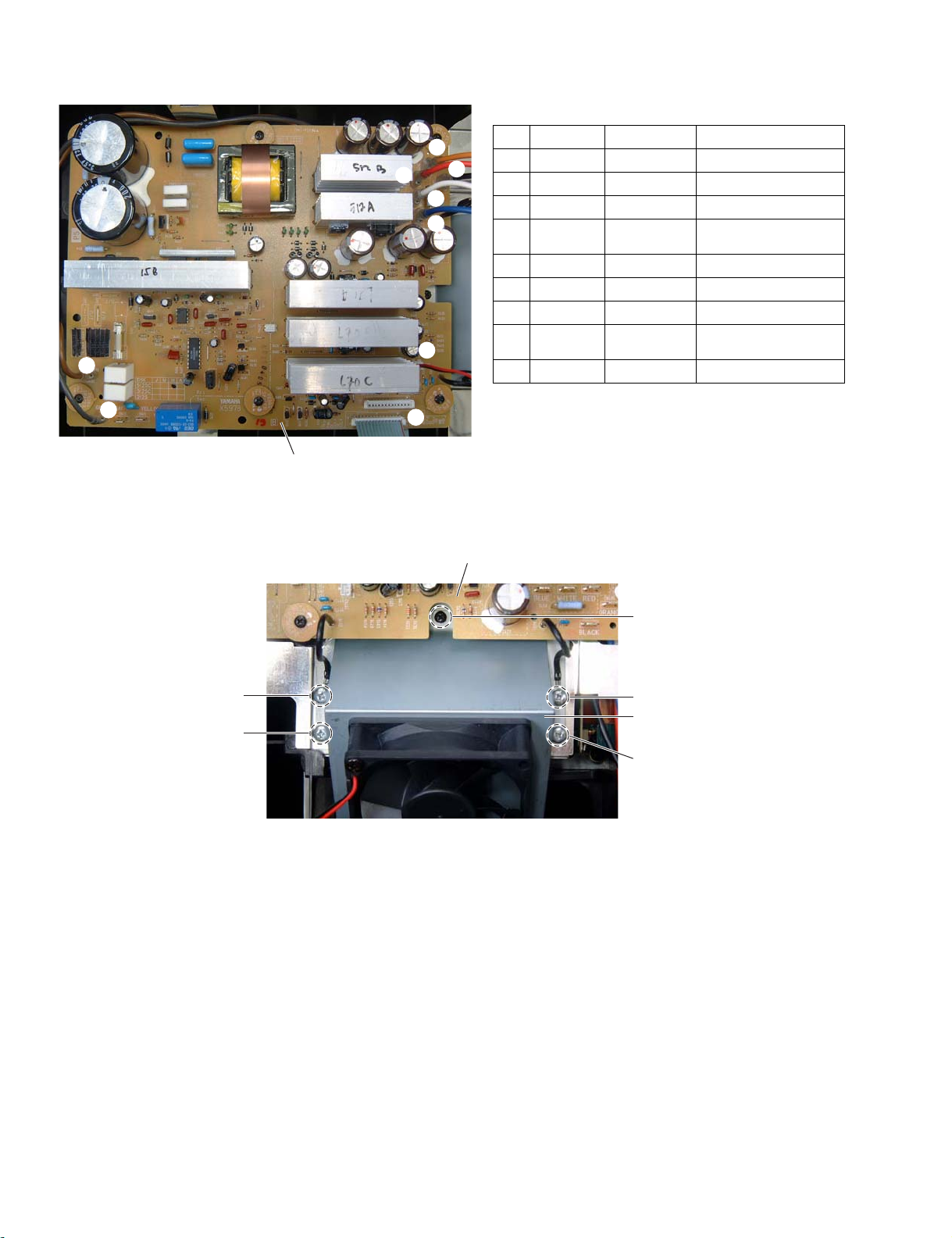
5. PS Circuit Board
(Time required: about 10 minutes)
5-1 Remove the front panel unit. (See procedure 1.)
5-2 Remove the wires specified in the Photo.4 and Table.2.
5-3 Remove the two (2) screws marked [628A] and the GND
wire. (Photo.5)
5-4 Remove the six (6) screws marked [640] and the spacers.
The PS circuit board can then be removed. (Fig.5)
Rear grounding brackets
(
リアグランド金具)
[624B]
PS circuit board
(PS
シート)
[628B]
[624A]
5. PS シー ト (所要時間 : 約 10 分)
5-1 フロントパネルユニット を外します。 (1 項参照)
5-2 写真 4および表2 の束線を外 し ます。
5-3 [628A] のネジ2 本を外し、アース線を外し ます。(写真 5)
5-4 [640] のネジ 6 本を外し、 PS シー ト を外し ます。 ( 図 5)
(サブ風防ケース)
Case
Fan(DCファン)
[628B]
[640]
Spacer (
[640]: Bind Head Tapping Screw-P 3x10 MFZN2W3 (WF001000) Pタイト+BIND
[624B]: Bind Head Tapping Screw-P 3x6 MFZN2W3 (WE877900) S タイト+BIND
[627]: Bind Head Screw 4x30 MFZN2W3 (WF105900) 小ネジ+ BIND
スペーサー)
Fig.5 (図 5)
[627]
19
EMX512SC/EMX312SC
Table.2(表 2)
2
1
PS circuit board (PSシート)
Photo.4 (写真 4)
No. Connector Color of Wire Connected to
1
2
3
4
4
5
6
8
7
5
6
7
8
3
9
9
PS circuit board (PSシート)
CN401 GRAY OUT Circuit Board
CN402 BROWN OUT Circuit Board
CN404 -- Fan
CN405 RED PA Circuit Board
(EMX512SC only)
CN406 ORANGE PA Circuit Board
CN407 BLACK OUT Circuit Board
CN408 BLUE PA Circuit Board
CN409 WHITE PA Circuit Board
(EMX512SC only)
CN415 -- Power amplifier unit
[628A]
[628B]
[624A]: Bind Head Tapping Screw-P 3x6 MFZN2W3 (WE877900) S タイト+BIND
[628A]: Bind Head Screw 4x8 MFZN2W3 (WE968500) 小ネジ+ BIND
[628B]: Bind Head Screw 4x8 MFZN2W3 (WE968500) 小ネジ+ BIND
Photo.5 (写真 5)
6. Fan (Time required: about 5 minutes)
6-1 Remove the front panel unit. (See procedure 1.)
6-2 Remove the PS circuit board. (See procedure 5.)
6-3 Remove the screw marked [624A]. (Fig.5 & Photo.5)
6-4 Remove the two (2) screws marked [628B]. The fan and
case can then be removed. (Fig.5 & Photo.5)
6-5 Remove the two (2) screws marked [627]. The fan can then
be separated from the case. (Fig.5)
[624A]
[628A]
Fan (DCファン)
[628B]
6. DC フ ァ ン (所要時間 : 約 5 分)
6-1 フロントパネルユニット を外します。 (1 項参照)
6-2 PS シー ト を外し ます。 (5 項参照 )
6-3 [624A] のネジ 1 本を外します。 ( 図5、写真5)
6-4 [628B] のネジ 2 本を外し、 DC フ ァ ン と サブ風防ケ ー ス
を外 し ます。 (図 5、写真5)
6-5 [627] のネジ2 本を外し、 DC ファンを外します。 ( 図 5)
20
EMX512SC/EMX312SC
7. Rear Panel Unit (Time required: about 5 minutes)
7-1 Remove the front panel unit. (See procedure 1.)
7-2 Remove the PS circuit board. (See procedure 5.)
7-3 Remove the fan. (See procedure 6.)
7-4 Remove the four (4) screws marked [624B] and the rear
grounding brackets. (Fig.5)
7-5 Remove the six (6) screws marked [630]. The rear panel unit
can then be removed. (Fig.1)
* When removing the rear panel only, remove the screws
marked with
▼ . (Fig.6)
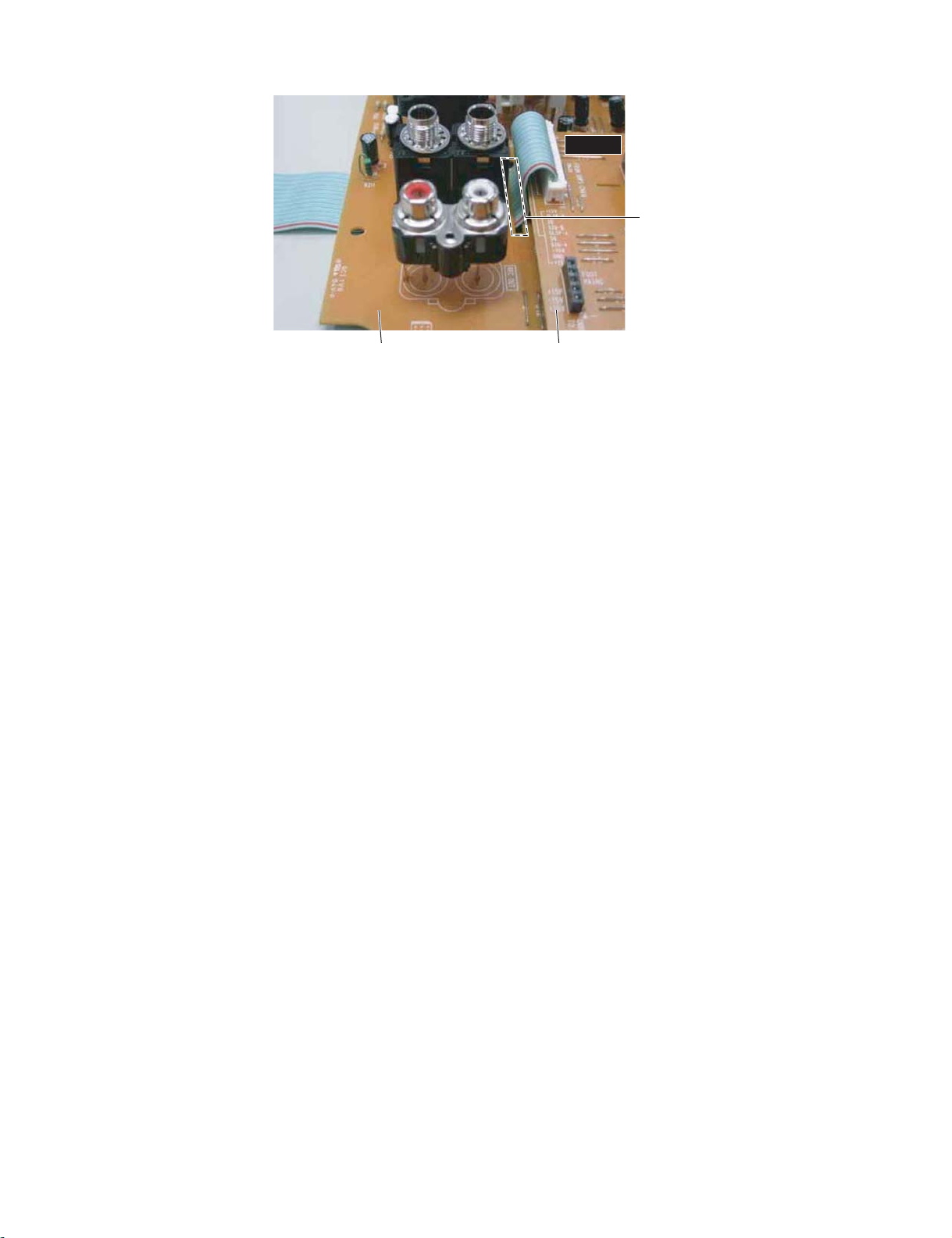
8. OUT Circuit Board
(Time required: about 10 minutes)
8-1 Remove the rear panel unit. (See procedure 7.)
8-2 Remove the wires (violet, yellow and black) from CN301,
CN302 and CN303 on the OUT circuit board. (Photo.6)
8-3 Remove the two (2) screws marked [190] and the spacer.
(Fig.6)
8-4 Remove the two (2) screws marked [150], two (2) screws
marked [170], four (4) screws marked [180] and two
hexagonal nuts. (Fig.1 & Fig.6)
8-5 Remove the screw marked [185] and the GND wire from the
AC inlet. The OUT circuit board can then be removed.
(Fig.6 & Photo.7)
7. リ アパネルユニ ッ ト (所要時間 : 約 5 分)
7-1 フロントパネルユニット を外します。 (1 項参照)
7-2 PS シー ト を外し ます。 (5 項参照)
7-3 DC ファンを外します。 (6項参照 )
7-4 [624B] のネジ 4 本を外し、 リ アグラン ド金具を外し ま
す。 ( 図5)
7-5 [630] のネジ 6 本を外し、 リ アパネルユニッ ト を外し ま
す。 ( 図1)
※ リ アパネル印刷上 り のみ を 取 り外す場合は、 ▼マー ク がつ
いたネジを外し ます。 (図 6)
8. OUT シー ト (所要時間 : 約 10 分)
8-1 リアパネルユニットを外します。(7 項参照)
8-2 OUT シー トの CN301、 CN302、 CN303 から束線( 紫、 黄
色、 黒 ) を外します。 ( 写真 6)
8-3 [190] のネジ 2 本とスペーサー1 個を外し ます。 ( 図6)
8-4 [150] のネジ 2 本、 [170] のネジ 2 本、 [180] のネジ 4 本、
六角ナ ッ ト 2 個を外します。 ( 図 1、図6)
8-5 [185] のネジ 1 本を外し、AC インレッ トからのアース線
を外し、 OUT シー ト を外し ます。 ( 図6、写真7)
[190]
OUT circuit board
(OUTシート)
<Rear panel unit>
Spacer
(スペーサー)
Case
(風防ケース)
[50]: Bind Head Screw 4x8 MFZN2B3 (WE969000) 小ネジ+ BIND
[130]: Bind Head Tapping Screw-S 3x6 MFZN2B3 (WE877800) S タイト+BIND
[150]: Bind Head Tapping Screw-S 3x6 MFZN2B3 (WE877800) S タイト+BIND
[170]: Bind Head Tapping Screw-B 3x12 MFZN2B3 (WE998100) B タイト+BIND
[180]: Flat Fillister H. Tapping 3x8 MFZN2W3 (WF790100) B タイト+平頭
[190]: Bind Head Tapping Screw-P 3x6 MFZN2W3 (WE877900) S タイト+BIND
[180]
[130]
Power amplifier unit
(パワーアンプユニット)
Hexagonal nut
(六角ナット)
[170]
[150]
[130]
[185]
[50]
Back(裏面)
Fig.6 (図 6)
21
EMX512SC/EMX312SC
CN303
[185]
CN302CN301
Photo.6 (写真 6)
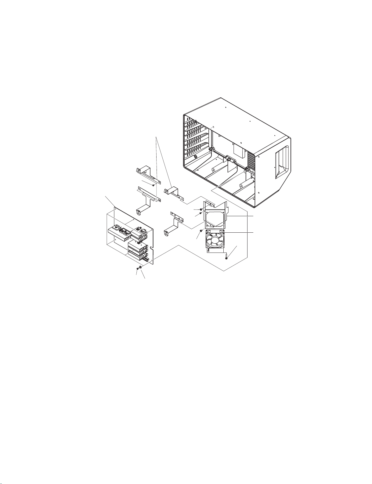
9. Power Amplifier Unit (Time required: about 10 minutes)
9-1 Remove the rear panel unit. (See procedure 7.)
9-2 Remove the OUT circuit board. (See procedure 8.)
9-3 Remove the five (5) screws marked [130]. (Fig.1 & Fig.6)
9-4 Remove the four (4) screws marked [50]. The power
amplifier unit then can be removed from the rear panel unit,
together with the case. (Fig.1 & Fig.6)
9-5 Remove the wires from the slit of the case. (Photo.8 &
Photo.9)
Slit (スリット) Slit (スリット)
[185]: Bind Head Screw 4x8 MFZN2W3 (WF106500) 小ネジ+ BIND
Photo.7 (写真 7)
9. パワーアン プユニ ッ ト (所要時間 : 約10 分)
9-1 リアパネルユニットを外します。(7 項参照)
9-2 OUT シー ト を外し ます。 (8 項参照)
9-3 [130] のネジ5 本を外します。 ( 図 1、図6)
9-4 [50] のネジ 4 本を外し、 パワーアンプユニ ッ ト と風防
ケース を リ アパネルユニッ ト から外し ます。( 図1、図 6)
9-5 束線 を 風防ケース の ス リ ッ ト か ら抜 き ます。
( 写真 8、写真9)
22
Photo.8 (写真 8) Photo.9 (写真 9)
EMX512SC/EMX312SC
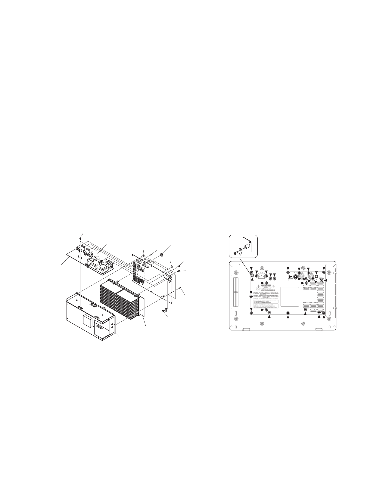
10. PA Circuit Board (Time required: about 10 minutes)
10-1 Remove the rear panel unit. (See procedure 7.)
10-2 Remove the OUT circuit board. (See procedure 8.)
10-3 Remove the power amplifier unit. (See procedure 9.)
10-4 Remove the fourteen (14) screws marked [50a]. (Fig.7)
10-5 Remove the twelve (12) screws (for EMX512SC) or four (4)
screws (for EMX312SC) marked [60a]. The PA circuit
board then can be removed. (Fig.7)
Radiation sheet
(
放熱シートC)
EMX512SC
[50a]
[60a]
Radiation sheet
(
放熱シートA)
10. PA シー ト (所要時間 : 約 10 分)
10-1 リアパネルユニットを外します。(7 項参照)
10-2 OUT シー ト を外し ます。 (8 項参照)
10-3 パワーアンプユニッ ト を外します。 (9 項参照 )
10-4 [50a] のネジ14 本を外します。 ( 図7)
10-5 EMX512SC の場合は [60a] のネジ 12 本、 EMX312SC の
場合は [60a] のネジ 4 本を外し、 PA シー ト を外し ます。
( 図7)
EMX312SC
[50a]
[60a]
[50a]
[50a]
[50a]
[60a]
[50a]
Radiation sheet
(
放熱シートD)
[60a]
[60a]
Radiation sheet
(
放熱シートB)
Heat sink
(
ヒートシンク)
[50a]: Bind Head Screw 3x12 MFZN2Y (VB763800) +バ イ ン ド 小ネジ
[60a]: Bind Head Tapping Screw-B 3x8 MFZN2BL (EP600190) +バイ ン ド B タ イ ト
Fig.7 (図 7)
23

EMX512SC/EMX312SC
■ LSI PIN DESCRIPTION(LSI 端子機能表)
AK5381VT-E2 (X5219A00) ADC (Analog to Digital Converter).......................... 24
PCM1742KEG/2K (X3538A00) DAC (Digital to Analog Converter).................... 24
MX23L8103TC-90G (X5922A00) CPU............................................................... 24
YMW767-VTZ (X6055A00) CPU......................................................................... 25
• AK5381VT-E2 (X5219A00) ADC (Analog to Digital Converter) DSP: ICM04
PIN
No. NAME I/O FUNCTION
1 AINR I Rch Analog input pin 9 SDTO O Audio serial data output pin
2 AINL I Lch Analog input pin 10 LRCK I/O Output channnel clock pin
3 CKS1 I Mode select 1 pin 11 MCLK I Master clock input pin
4 VCOM O Common voltage output pin 12 SCLK I/O Audio serial data clock pin
5 AGND - Analog ground 13 PDN I Power down mode pin
6 VA - Analog power supply 14 DIF I Audio interface format pin
7 VD - Digital power supply 15 CKS2 I Mode select 2 pin
8 DGND - Digital ground 16 CKS0 I Mode select 0 pin
• PCM1742KEG/2K (X3538A00) DAC (Digital to Analog Converter) DSP: ICM08
PIN
No. NAME
1 BCK IN Audio Data Bit Clock Input.
2 DATA IN Audio Data Digital Input.
3 LRCK IN L-Channel and R-Channel Audio Data
4 DGND Digital Ground 12 ZEROL/NA
5V
6V
7V
OUT
8V
OUT
DD
CC
TYPE
Latch Enable Input.
Digital Power Supply, +3.3V 13 MD IN Mode Control Data Input.
Analog Power Supply, +5V 14 MC IN Mode Control Clock Input.
L
OUT
R
Analog Output for L-Channel. 15 ML IN Mode Control Latch Input.
OUT
Analog Output for R-Channel. 16 SCK IN System Clock Input.
FUNCTION
(1)
(1)
(1)
PIN
No. NAME I/O FUNCTION
PIN
No. NAME
9 AGND Analog Ground
10 V
COM
11 ZEROR/
ZEROA
TYPE
Common Voltage Decoupling.
OUT
Zero Flag Output for R-Channel/Zero Flag
Output for L/R-Channel.
OUT
Zero Flag Output for L-Channel/No Assign.
FUNCTION
(2)
(2)
(2)
NOTES: (1) Schmitt-trigger input, 5V tolerant. (2) Schmitt-trigger with internalpull-down, 5V tolerant.
• MX23L8103TC-90G (X5922A00) CPU DSP: ICM10
PIN
No. NAME I/O FUNCTION
1A15 I
2 A14 I 26 CE# I Chip enable
3 A13 I 27 VSS - Ground
4 A12 I 28 OE# I Output enable
5A11 I 29 D0 O
6A10 I 30 D8 O
7A9 I 31D1 O
8A8 I 32D9 O
9 (N.C.) 10 (N.C.) - 34 D10 O
11 (N.C.) - 35 D3 O
12 (N.C.) - 36 D11 O
13 (N.C.) - 37 VCC - Power supply +3.3 V
14 (N.C.) - 38 D4 O
15 (N.C.) - 39 D12 O
16 A18 I
17 A17 I 41 D13 O
18 A7 I 42 D6 O
19 A6 I 43 D14 O
20 A5 I 44 D7 O
21 A4 I 45 D15/A-1 I/O Data bus / LSB address
22 A3 I 46 VSS - Ground
23 A2 I 47 BYTE# - Word/byte mode selection
24 A1 I 48 A16 I Address bus
Address bus
(Unused)
Address bus
PIN
No. NAME I/O FUNCTION
25 A0 I Address bus
33 D2 O
40 D5 O
Data bus
Data bus
24
EMX512SC/EMX312SC
• YMW767-VTZ (X6055A00) CPU DSP: ICM07
PIN
No. NAME I/O FUNCTION
1 VSS - VSS 65 VSS - VSS
2 TESTN I Input for TEST 66 IOVDD - IOVDD +3.3V
3 PLLBPN I PLL bypass select 67
4 PLLVDD - PLLVDD +2.5V 68
5 CIN - Capacitor terminal for PLL 69 RDN/PF4 O External memory read enable
6 PLLVSS - PLLVSS 70 MD00 I/O
7TRSTN I
8 TMS I 72 MD01 I/O
9 TCK I 73 MD09 I/O
10 TDI I 74 MD02 I/O
11 TD0 O JTAG output 75 MD10 I/O
12 XI I Crystal oscillator 76 MD03 I/O
13 XO O Crystal oscillator 77 VSS - VSS
14 VSS - VSS 78 MD11 I/O
15 VDD - VDD +2.5V 79 MD04 I/O
16 ICN I Hardware reset 80 MD12 I/O
17 ECSN I CPU I/F chip select 81 MD05 I/O
18 EWRN/PD5 I CPU I/F write enable 82 MD13 I/O
19 ERDN/PD4 I CPU I/F read enable 83 MD06 I/O
20 EA3/PD3 I
21 EA2/PD2 I 85 MD07 I/O
22 EA1/PD1 I 86 MD15 I/O
23 EA0/PD0 I 87 WRN/PF5 O External memory write enable
24 IOVDD - IOVDD +3.3V 88 VSS - VSS
25 ED0/PC0 I/O
26 ED1/PC1 I/O 90 IOVDD - IOVDD +3.3V
27 ED2/PC2 I/O 91 MA17 O
28 ED3/PC3 I/O 92 MA16 O
29 ED4/PC4 I/O 93 MA15 O
30 ED5/PC5 I/O 94 MA14 O
31 ED6/PC6 I/O 95 MA13 O
32 ED7/PC7 I/O 96 MA12 O
33 VSS - VSS 97 MA11 O
34 IRQ0N/PH0 I Interrupt input 98 MA10 O
35 TxD0 O Serial output 99 MA09 O
36 RxD0 I serial input 100 MA08 O
37 TxD1/PG2 O Serial output 101 MA07 O
38 RxD1/PH1 I serial input 102 MA06 O
39 SCLK1/PH2 I External synchronization clock 103 MA05 O
40 SD0 O Serial output 104 VSS - VSS
41 SDI/PH3 I serial input 105 MA04 O
42 BCLK O Bit clock output 106 MA03 O
43 WCLK/SY0 O Word clock output 107 MA02 O
44
SYSCLK/PG3
45 VSS - VSS 109 CS0N/PG0 O External memory chip select
46 VDD - VDD +2.5V 110 MA18 O
47 IOVDD - IOVDD +3.3V 111 MA19 O
48 PA0 I/O
49 PA1 I/O 113 MA22/PF2 O
50 PA2 I/O 114 MA20 O
51 PA3 I/O 115 MA23/PF3 O External memory address bus
52 PA4 I/O 116 CS1N/PG1 O External memory chip select
53 PA5 I/O 117 MA00/PF0 O
54 PA6 I/O 118 VSS - VSS
55 PA7 I/O 119 VDD - VDD +2.5V
56 VSS - VSS 120 IOVDD - IOVDD +3.3V
57 PB0 I/O
58 PB1 I/O 122 CS3N/PE1 O
59 PB2 I/O 123
60 PB3 I/O 124 CS5N/PE3 O
61 PB4 I/O 125
62 PB5 I/O 126
63 PB6 I/O 127
64 PB7/SYI I/O 128
JTAG input
CPU I/F address bus
CPU I/F data bus
O Clock output 108 MA01 O
I/O port
I/O port
PIN
No. NAME I/O FUNCTION
LBN/LWRN/PF6
UBN/UWRN/PF7
71 MD08 I/O
84 MD14 I/O
89 VDD - VDD +2.5V
112 MA21/PF1 O
121 CS2N/PE0 O
CS4N/CASN/PE2
CS50RDN/PE4
CS51WRN/PE5
CS52WRN/PE6
CS53WRN/RASN/PE7
O External memory lower-byte enable
O External memory upper-byte enable
External memory data bus
External memory data bus
External memory address bus
External memory address bus
External memory address bus
O
External memory chip select
O
O
O
O
25
EMX512SC/EMX312SC
■ IC BLOCK DIAGRAM(IC ブロック図)
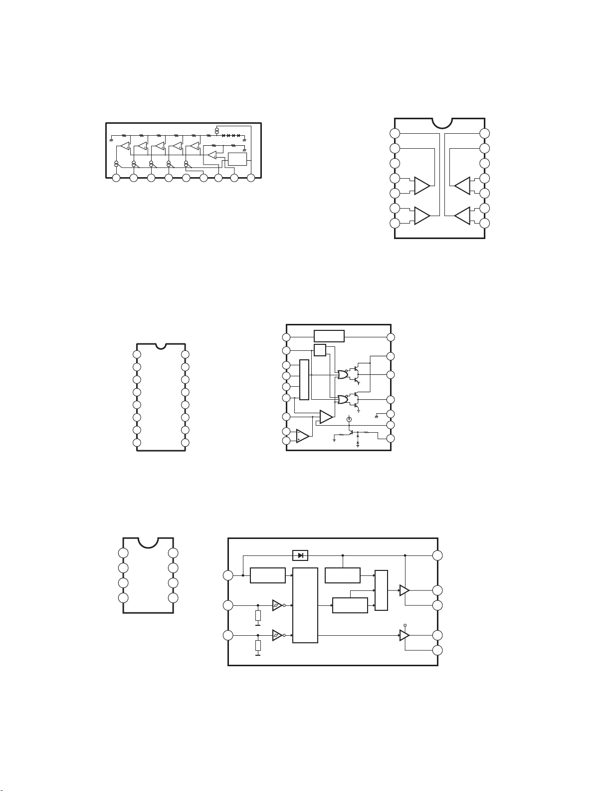
• PST596DNR (X0165A00)
System Reset
DSP: ICM03
M/R
SUB
GND
1
2
3
54Vcc
VOUT
Vcc
M/R
5
1
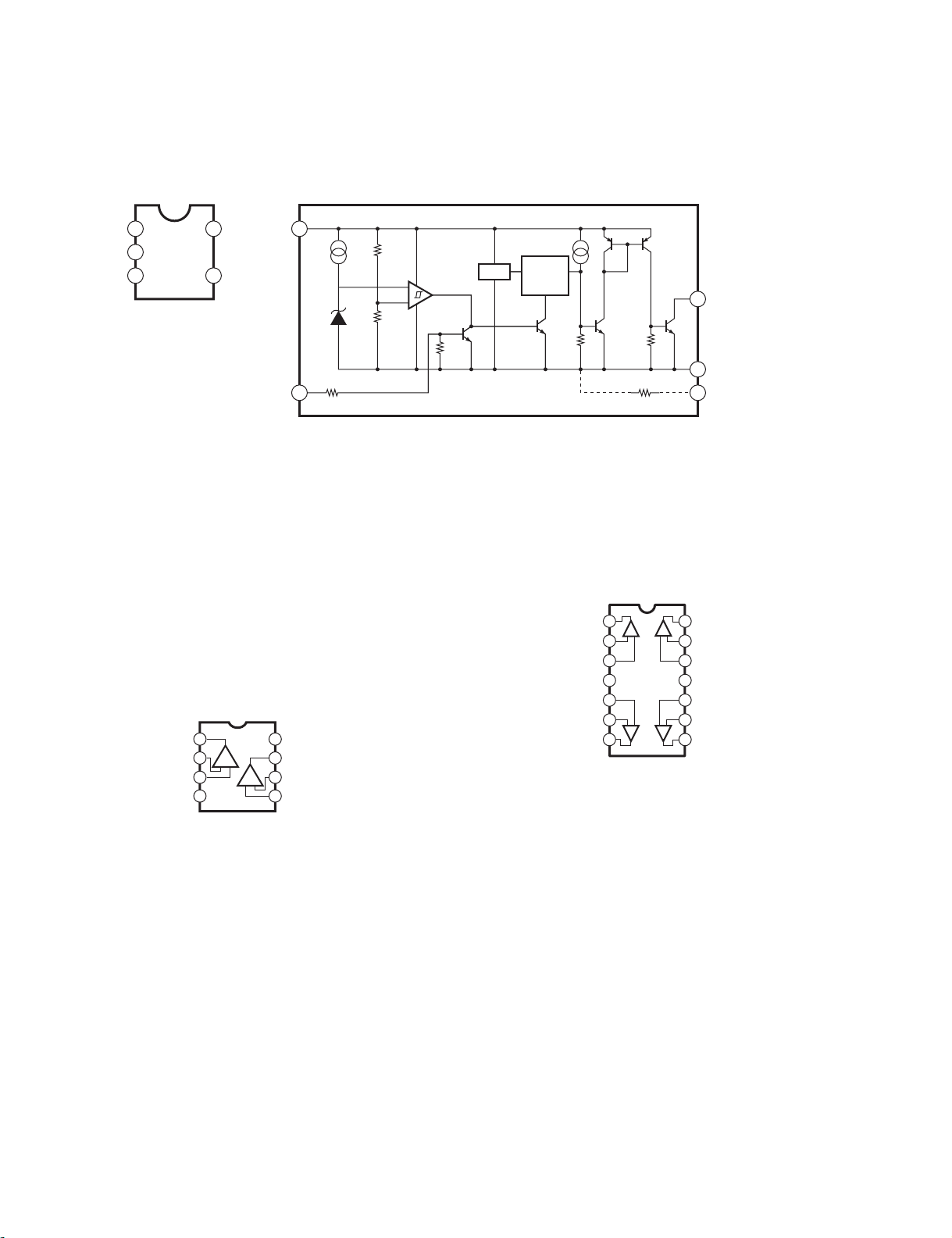
• NJM2068M-D (TE2) (X3505A00)
NJM4558M-TE1 (X5676A00)
Dual Operational Amplifier
DSP: ICM09, ICM11
JACK: IC001-IC012, IC101, IC102, IC106, IC201, IC202,
IC206
MIX: IC001-IC006, IC101-IC105, IC201-IC205,
IC301-IC306, IC408-IC411
PA: IC101
+-
+DC Voltage
8
Supply
Output B
7
Inverting
6
Input B
Non-Inverting
5
Input B
Output A +V
Inverting
Input A
Non-Inverting
Input A
-DC Voltage Supply
1
2
3
4 -V
+-
Delay
–
OSCRTQ
+
–
4
OUT
V
3
GND
SUB
2
• NJM2060M (XM560A00)
Quad Operational Amplifier
MIX: IC401-IC406
D OUTPUT
14
+
D –INPUT
13
D +INLPUT
12
V–
11
C +INPUT
10
C –INPUT
9
+
C
C OUTPUT
8
A –INPUT
A +INPUT
B +INPUT
B –INPUT
B OUTPUT
V+
1A OUTPUT
AD
+
2
3
4
5
6
+
––
B
7
26
EMX512SC/EMX312SC
• LB1423N (XZ348A00)
LED Driver
MIX: IC412-IC414
+ + + + +
1D22D33D44
D1
GND5D56Amp
+
7IN8
Output
• SG3525AN (X2383A00)
Regulating Pulse Width Modulator
PS: IC401
N.I. INPUT
SYNC
OSC. OUTPUT
DISCHARGE
SOFT-START
1INV. INPUTN
2
3
4
5
C
T
6
R
T
7
8
REF
V
16
+V
15
IN
OUTPUT B
14
V
13
C
GROUND
12
11
OUTPUT A
10
SHUTDOWN
9
COMPENSATION
Constant
Current
Circuit
9
CC
V
V
OSC. OUTPUT
SYNC
DISCHARGE
COMPENSATION
INV. INPUTN
N.I. INPUT
• BA10339F (X6266A00)
Comparator
PA: IC102
OSCILLATOR
E/A
REFERENCE
REGULATOR
FLIP/
FLOP
PWM
A
B
50µA
5K
16 15
REF
4
3
R
6
T
7
C
5
T
9
1
2
1
OUT2
2
OUT1
3
Vcc
4
–IN1
+IN1
–IN2
+IN2
5K
5
6
7
13
11
14
12
8
10
+V
IN
V
C
OUTPUT A
OUTPUT B
GROUND
SOFT-START
SHUTDOWN
–
+
–
+
14
OUT3
13
OUT4
12
GND
11
+IN4
+
–
10
–IN4
9
+IN3
+
–
8
–IN3
• L6385 (X5908A00)
Driver
PS: IC402
1
LIN
2
HIN
3
Vcc
4
GND
86Vboot
7 HVG
OUT
5LVG
Vcc
HIN
BOOTSTRAP DRIVER
8
Vboot
3
2
UV
DETECTION
LOGIC
UV
DETECTION
LEVEL
SHIFTER
R
R
S
HVG
DRIVER
7
HVG
6
OUT
Vcc
1
LIN
LVG
DRIVER
5
LVG
4
GND
27
EMX512SC/EMX312SC
■ CIRCUIT BOARDS(シート基板図)
• Contents(目次)
SPACER Circuit Board (X6384D0) ..................................................28
SW Circuit Board (X5967B0)............................................................ 28
DSP Circuit Board (X5022C0) .......................................................... 29
JACK Circuit Board (X5969B0) ........................................................30
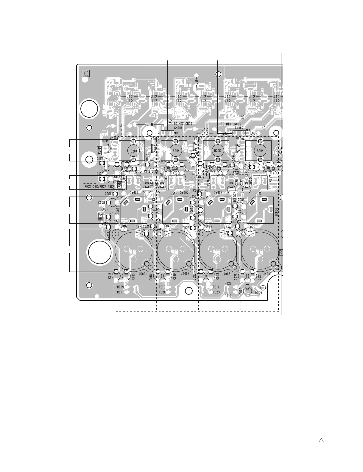
MIX Circuit Board (X5967B0) ........................................................... 36
OUT Circuit Board (X6384D0).......................................................... 42
PA Circuit Board (X5971C0) ............................................................ 44
PS Circuit Board (X5978C0) ............................................................ 48
Note: See parts list for details of circuit board component parts.
注 : シー ト の部品詳細はパーツ リス ト をご参照 く だ さ い。
• SPACER Circuit Board
• SW Circuit Board
POWER
ON/ON/ OFF
Pattern side(パターン側)Component side(部品側)
2NA-WE83470
GRAY
to PS-CN410
to PS-CN411
YELLOW
Component side(部品側) Pattern side(パターン側)
2
28
2NA-WD94320
3
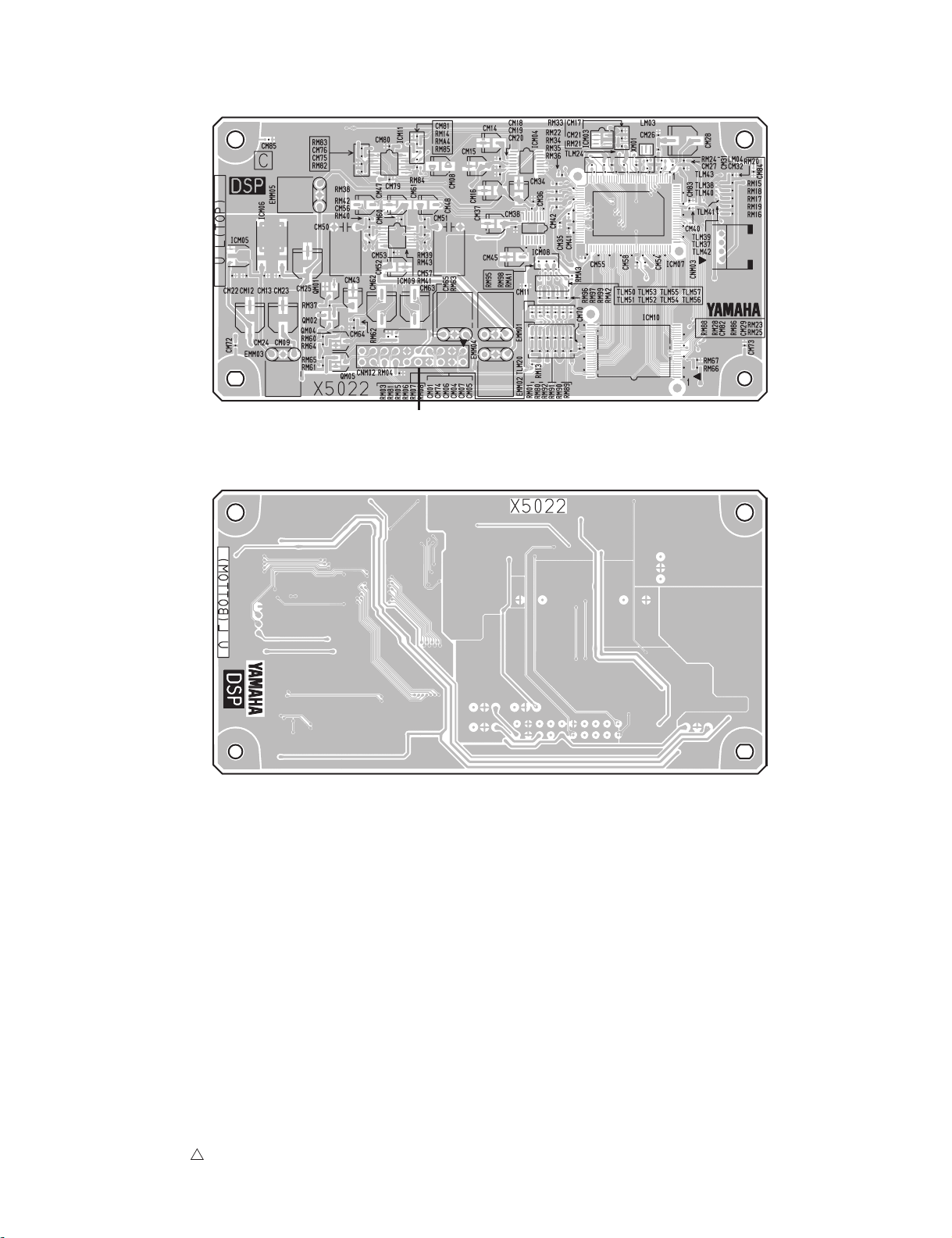
• DSP Circuit Board
EMX512SC/EMX312SC
N.C.
to MIX-CN301
Component side(部品側)
Pattern side(パターン側)
2NA-WD80120
2
29
EMX512SC/EMX312SC
• JACK Circuit Board
COMP
LINE/MIC
A
to MIX-CN001 to MIX-CN002
INPUT A
INPUT B
1 234
A’
Component side(部品側)
30
2NA-WD94340
2
 Loading...