

Page 1

DSP-AX1/RX-V1
AV AMPLIFIER/AV RECEIVER
DSP-AX1/RX-V1
SERVICE MANUAL
This manual has been provided for the use of authorized YAMAHA Retailers and their service personnel.
It has been assumed that basic service procedures inherent to the industry, and more specifically YAMAHA Products, are already
known and understood by the users, and have therefore not been restated.
WARNING: Failure to follow appropriate service and safety procedures when servicing this product may result in personal
IMPORTANT: The presentation or sale of this manual to any individual or firm does not constitute authorization, certification
The data provided is believed to be accurate and applicable to the unit(s) indicated on the cover. The research, engineering, and
service departments of YAMAHA are continually striving to improve YAMAHA products. Modifications are, therefore,
inevitable and specifications are subject to change without notice or obligation to retrofit. Should any discrepancy appear to exist,
please contact the distributor's Service Division.
WARNING: Static discharges can destroy expensive components. Discharge any static electricity your body may have
IMPORTANT: Turn the unit OFF during disassembly and part replacement. Recheck all work before you apply power to the
injury, destruction of expensive components, and failure of the product to perform as specified. For these
reasons, we advise all YAMAHA product owners that any service required should be performed by an
authorized YAMAHA Retailer or the appointed service representative.
or recognition of any applicable technical capabilities, or establish a principle-agent relationship of any
form.
accumulated by grounding yourself to the ground buss in the unit (heavy gauge black wires connect to this
buss).
unit.
■ CONTENTS
TO SERVICE PERSONNEL ........................................... 1
FRONT PANELS ............................................................. 2
REAR PANELS ........................................................... 3~4
SPECIFICATIONS ....................................................... 5~8
INTERNAL VIEW ............................................................ 9
DISASSEMBLY PROCEDURES .............................. 9~10
SELF DIAGNOSIS FUNCTION............................... 11~32
AMP ADJUSTMENTS ................................................... 33
IMPORTANT NOTICE
DSP-AX1/RX-V1
TUNER ADJUSTMENTS ........................................ 34~37
IC DATA .................................................................. 38~53
PRINTED CIRCUIT BOARD ................................... 54~83
BLOCK DIAGRAM .................................................. 84~88
PIN CONNECTION DIAGRAM ..................................... 89
SCHEMATIC DIAGRAM ....................................... 90~101
PARTS LIST ........................................................ 102~135
REMOTE CONTROL TRANSMITTER................ 136~141
100698
Page 2
DSP-AX1/RX-V1
■ TO SERVICE PERSONNEL
1. Critical Components Information.
Components having special characteristics are marked Z
and must be replaced with parts having specifications equal
to those originally installed.
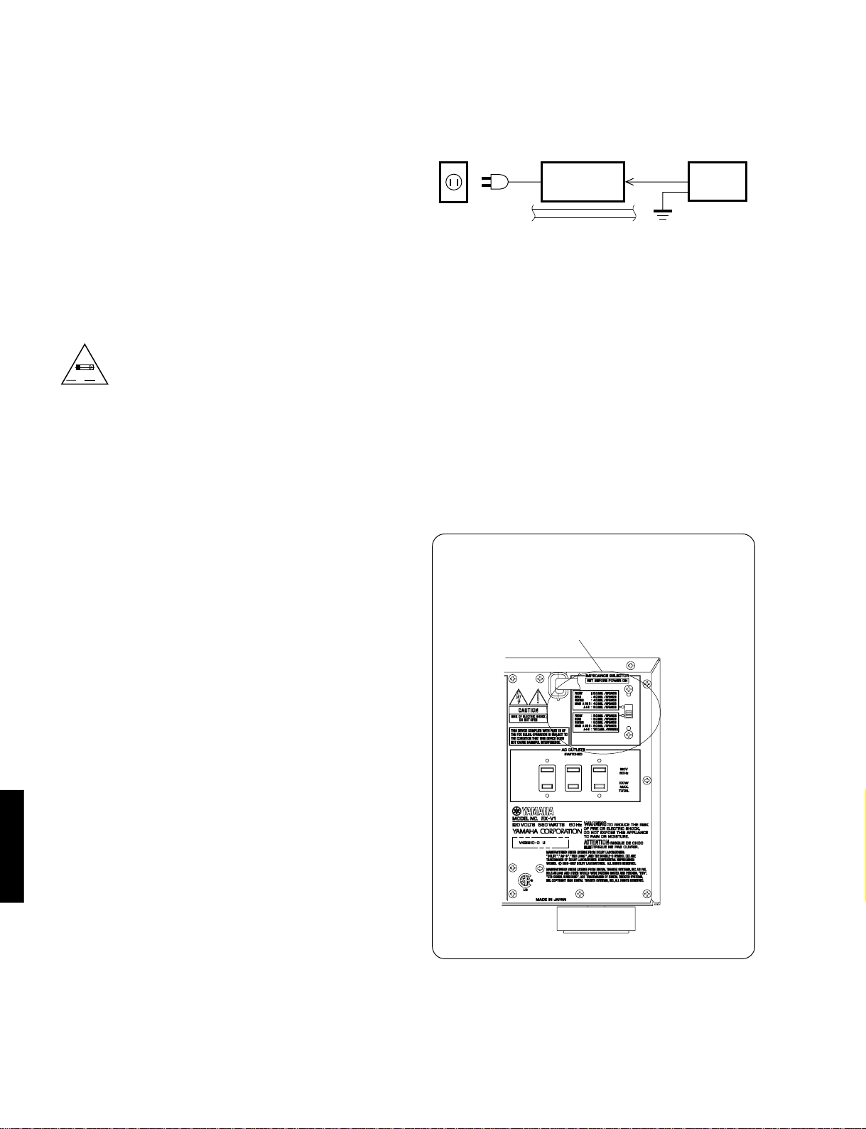
2. Leakage Current Measurement (For 120V Models Only).
When service has been completed, it is imperative to verify
that all exposed conductive surfaces are properly insulated
from supply circuits.
● Meter impedance should be equivalent to 1500 ohm shunted
by 0.15µF.
● Leakage current must not exceed 0.5mA.
“CAUTION”
“F751 : FOR CONTINUED PROTECTION AGAINST RISK OF FIRE, REPLACE ONLY WITH SAME TYPE 12A, 250V FUSE.”
A V
CAUTION
F751 : REPLACE WITH SAME TYPE 12A, 250V FUSE.
WALL
OUTLET
● Be sure to test for leakage with the AC plug in both
polarities.
EQUIPMENT
UNDER TEST
INSULATING
TABLE
AC LEAKAGE
TESTER OR
EQUIVALENT
WARNING: CHEMICAL
CONTENT NOTICE!
The solder used in the production of this product
contains LEAD. In addition, other electrical/
electronic and/or plastic (where applicable)
components may also contain traces of chemicals
found by the California Health and Welfare
Agency (and possibly other entities) to cause
cancer and/or birth defects or other reproductive
harm.
DO NOT PLACE SOLDER, ELECTRICAL/
ELECTRONIC OR PLASTIC COMPONENTS IN
YOUR MOUTH FOR ANY REASON
WHATSOEVER!
Avoid prolonged, unprotected contact between
solder and your skin! When soldering, do not
inhale solder fumes or expose eyes to solder/flux
vapor!
If you come in contact with solder or components
located inside the enclosure of this product, wash
DSP-AX1/RX-V1
your hands before handling food.
ATTENTION
F751 : UTILISER UN FUSIBLE DE RECHANGE DE MEME TYPE DE 12A, 250V.
WARNING
Do not change the IMPEDANCE SELECTOR
switch setting while the power to this unit is
on, otherwise this unit may be damaged.
IMPEDANCE SELECTOR
1
Page 3
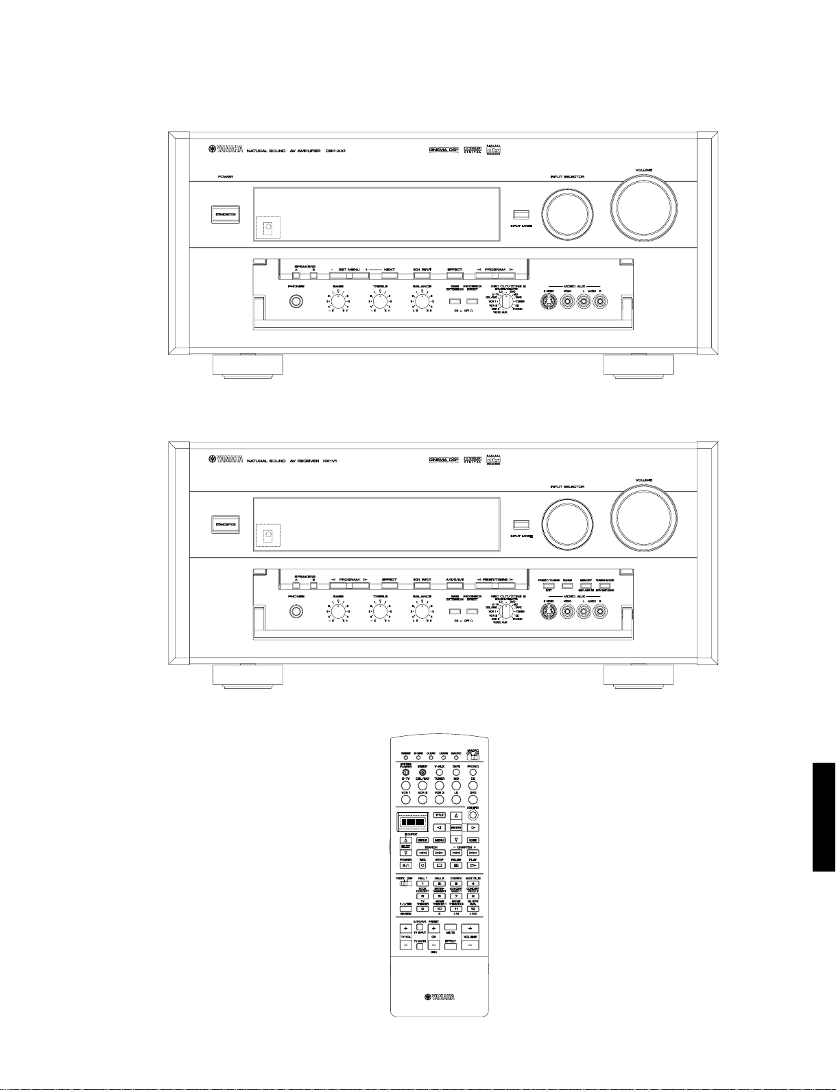
■ FRONT PANELS
▼ DSP-AX1
DSP-AX1/RX-V1
▼ RX-V1
DSP-AX1/RX-V1
2
Page 4
DSP-AX1/RX-V1
CCIB
*
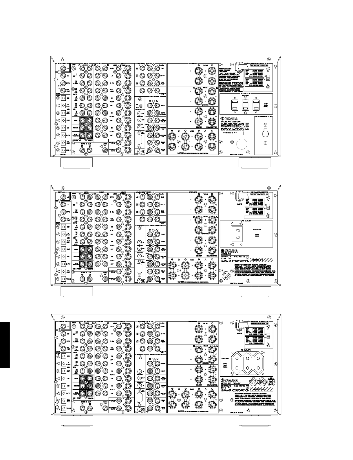
■ REAR PANELS
▼ DSP-AX1 R, T models
▼ DSP-AX1 B model
▼ DSP-AX1 G model
DSP-AX1/RX-V1
3
Page 5

▼ RX-V1 U model
DSP-AX1/RX-V1
▼ RX-V1 C model
▼ RX-V1 A model
DSP-AX1/RX-V1
4
Page 6

DSP-AX1/RX-V1
■ SPECIFICATIONS
■ AUDIO SECTION
Minimum RMS Output Power per Channel
MAIN, 20Hz to 20kHz, 0.015% THD, 8Ω . . . .110W+110W
CENTER, 20Hz to 20kHz, 0.015% THD, 8Ω . . . . . . 110W
REAR, 20Hz to 20kHz, 0.015% THD, 8Ω . . .110W+110W
REAR CENTER,
20Hz to 20kHz, 0.015% THD, 8Ω . . . . . . . . . . . . . . 110W
FRONT, 1kHz, 0.05% THD, 8Ω . . . . . . . . . . . . .35W+35W
Maximum Power per Channel (R, T models only)
MAIN, 1kHz, EIAJ, 10% THD, 8Ω . . . . . . . . .150W+150W
CENTER, 1kHz, EIAJ, 10% THD, 8Ω . . . . . . . . . . . 150W
REAR, 1kHz, EIAJ, 10% THD, 8Ω . . . . . . . . .150W+150W
REAR CENTER, 1kHz, EIAJ, 10% THD, 8Ω . . . . . . 150W
FRONT, 1kHz, EIAJ, 10% THD, 8Ω . . . . . . . . . .45W+45W
Dynamic Power per Channel (U, C, R, T models only)
MAIN, 8/6/4/2Ω . . . . . . . . . . . . . . . . . . . 150/180/240/340W
Dynamic Headroom (U, C, R, T models only)
8Ω . . . . . . . . . . . . . . . . . . . . . . . . . . . . . . . . . . . . . . 1.3dB
DIN Standard Output Power per Channel (B, G models only)
MAIN, 1kHz, 0.7% THD, 4Ω . . . . . . . . . . . . . .180W+180W
CENTER, 1kHz, 0.7% THD, 4Ω . . . . . . . . . . . . . . . . 180W
REAR, 1kHz, 0.7% THD, 4Ω . . . . . . . . . . . . .180W+180W
REAR CENTER, 1kHz, 0.7% THD, 4Ω . . . . .180W+180W
FRONT, 1kHz, 0.7% THD, 4Ω . . . . . . . . . . . . . .60W+60W
IEC Power (B, G models only)
MAIN, 1kHz, 0.015% THD, 8Ω . . . . . . . . . . . . . . . . . 120W
Power Band Width
MAIN, 0.04% THD, 55W/8Ω . . . . . . . . . . . . 10Hz to 50kHz
Damping Factor
MAIN/CENTER, 20Hz to 20kHz, 8Ω . . . . . . . 200 or more
Input Sensitivity/Impedance
PHONO MM . . . . . . . . . . . . . . . . . . . . . . . . . . 2.5mV/47kΩ
CD, etc . . . . . . . . . . . . . . . . . . . . . . . . . . . . . 150mV/47kΩ
MAIN IN . . . . . . . . . . . . . . . . . . . . . . . . . . . . . . . . . 1V/47kΩ
Maximum Input Signal Level
PHONO MM, 1kHz, 0.05% THD, (Effect on) . . . . . 100mV
CD, etc, (Effect on) . . . . . . . . . . . . . . . . . . . . . . . . . . . 2.3V
Output Level/Impedance
REC OUT . . . . . . . . . . . . . . . . . . . . . . . . . . . 150mV/600Ω
PRE OUT (MAIN, etc) . . . . . . . . . . . . . . . . . . . . . 1V/1.2kΩ
SUB WOOFER (EFFECT OFF, MAIN SP : SMALL)
SPLIT . . . . . . . . . . . . . . . . . . . . . . . . . . . . . . . . . . . .
MONO . . . . . . . . . . . . . . . . . . . . . . . . . . . . . . . . . . .
Maximum Voltage Output (20Hz to 20kHz, 1% THD)
PRE OUT (MAIN L/R) . . . . . . . . . . . . . . . . . . . . . . . . . . .3V
Headphone Jack Rated Output/Impedance
CD, etc, (40mV, 8Ω) . . . . . . . . . . . . . . . . . . . 150mV/100Ω
Frequency Response (10Hz to 100kHz)
CD, etc, MAIN L/R . . . . . . . . . . . . . . . . . . . . . . . +0/-3.0dB
RIAA Equalization Deviation (20Hz to 20kHz)
PHONO MM . . . . . . . . . . . . . . . . . . . . . . . . . . . . . 0±0.5dB
Tone Control Characteristics
BASS : Boost/cut . . . . . . . . . . . . . . . . . . . ±10dB (50Hz)
DSP-AX1/RX-V1
TREBLE : Boost/cut . . . . . . . . . . . . . . . . . . ±10dB (20kHz)
Center Graphic Equalizer
Bass Extension . . . . . . . . . . . . . . . . . . . . . . . . . . +6dB (60Hz)
Filter Characteristics
SUB WOOFER OUT : L.P.F. . . . . . . fc = 90Hz, 24dB/oct.
2.0V/1.2kΩ
4.0V/1.2kΩ
Turnover Frequency . . . . . . . . . . . . . . . . 350Hz
Turnover Frequency . . . . . . . . . . . . . . . 3.5kHz
Frequency . . . . . . . . . . . . 100/300/1k/3k/10kHz
Boost/cut . . . . . . . . . . . . . . . . . . . . . . . . . . ±6dB
Q . . . . . . . . . . . . . . . . . . . . . . . . . . . . . . . . . 0.7
Cinema Equalizer
HIgh Frequency . . . . . . . . . . . . . . . .1kHz to 12.7kHz
Boost/cut . . . . . . . . . . . . . . . . . . . -9dB to +6dB
PEQ Frequency . . . . . . . . . . . . . . . .1kHz to 12.7kHz
Boost/cut . . . . . . . . . . . . . . . . . . . -9dB to +6dB
Q . . . . . . . . . . . . . . . . . . . . . . . . . . . . . . . . 1.85
Total Harmonic Distortion (20Hz to 20kHz)
PHONO MM to REC OUT (1V) . . . . . . . . . . . . . . . . 0.01%
CD, etc, to PRE OUT MAIN L/R (1V) . . . . . . . . . . 0.005%
MAIN IN to L/C/R SP OUT (55W/8Ω) . . . . . . . . . . 0.005%
Signal-to-Noise Ratio (IHF-A-Network)
PHONO MM, Input Shorted 5mV (Effect off) . . . . . . . 86dB
CD, etc, Input Shorted (Effect off) . . . . . . . . . . . . . . . 96dB
Residual Noise (IHF-A-Network)
MAIN, SP OUT . . . . . . . . . . . . . . . . . . . . . . . . . . . . .150µV
Channel Separation (Vol. –30dB, Effect off)
PHONO MM, Input Shorted, 1kHz/10kHz . . . . 70dB/60dB
CD, etc, Input 5.1kΩ Shorted, 1kHz/10kHz . . . 70dB/60dB
Muting . . . . . . . . . . . . . . . . . . . . . . . . . . . . . . . . . . . . . . . . – ∞
■ VIDEO SECTION
Video Signal Type
U, C models . . . . . . . . . . . . . . . . . . . . . . . . . . . . . . . NTSC
A, B.G models . . . . . . . . . . . . . . . . . . . . . . . . . . . . . . . .PAL
R, T models . . . . . . . . . . . . . . . . . . . . . . . . . . . . NTSC/PAL
Composite Video Signal Level . . . . . . . . . . . . . . 1Vp-p/75Ω
S-Video Signal Level
Y . . . . . . . . . . . . . . . . . . . . . . . . . . . . . . . . . . . . 1Vp-p/75Ω
C . . . . . . . . . . . . . . . . . . . . . . . . . . . . . . . . . 0.286Vp-p/75Ω
Component Signal Level
Y . . . . . . . . . . . . . . . . . . . . . . . . . . . . . . . . . . . . 1Vp-p/75Ω
Cb/Cr . . . . . . . . . . . . . . . . . . . . . . . . . . . . . . . . . . 0.7V/75Ω
Video Maximum Input Level . . . . . . . . . . . . . . . . . . . 1.5Vp-p
Video Signal-to-Noise Ratio . . . . . . . . . . . . . . . . . . . . . 50dB
Monitor Output Frequency Response
Composite Video Signal . . . . . . . . . . . . 5Hz~10MHz, –3dB
S-Video Signal . . . . . . . . . . . . . . . . . . . . 5Hz~10MHz, –3dB
Component Signal . . . . . . . . . . . . . . . . . DC~20MHz, –3dB
5
Page 7
DSP-AX1/RX-V1
■ FM SECTION (RX-V1 only)
Tuning Range
U, C models . . . . . . . . . . . . . . . . . . . . . . .87.5 to 107.9MHz
A models . . . . . . . . . . . . . . . . . . . . . . .87.50 to 108.00MHz
50dB Quieting Sensitivity (IHF, 75 Ω)
U, C models only
Mono (1kHz, 100% Mod.) . . . . . . . . . . . . 1.6µV (15.3dBf)
Stereo (1kHz, 100% Mod.) . . . . . . . . . . . . 23µV (38.5dBf)
Usable Sensitivity (DIN, 75 Ω)
A model only
Mono (S/N 26dB) . . . . . . . . . . . . . . . . . . . . . . . . . . 0.9µV
Stereo (S/N 46dB) . . . . . . . . . . . . . . . . . . . . . . . . . . . 28µV
Alternate Channel Selectivity (± 400Hz)
U, C models . . . . . . . . . . . . . . . . . . . . . . . . . . . . . . . . . 75dB
Selectivity (two signals, 40kHz Dev.) (± 300Hz)
A model . . . . . . . . . . . . . . . . . . . . . . . . . . . . . . . . . . . . 55dB
Signal-to-Noise Ratio
U, C models
Mono/Stereo (IHF) . . . . . . . . . . . . . . . . . . . . . . . 81/75dB
A model
Mono/Stereo (DIN-weighted, 40kHz Dev.) . . . . . 75/69dB
Harmonic Distortion
Mono/Stereo (1kHz) . . . . . . . . . . . . . . . . . . . . . . . 0.1/0.2%
Stereo Separation
1kHz . . . . . . . . . . . . . . . . . . . . . . . . . . . . . . . . . . . . . . . 48dB
Frequency Response
20Hz to 15kHz . . . . . . . . . . . . . . . . . . . . . . . . . . . . 0±1.0dB
Output Level
U, C models
FM 100% mod. 1kHz . . . . . . . . . . . . . . . . . . . . . . 550mV
A models
FM 40kHz Dev. 1kHz . . . . . . . . . . . . . . . . . . . . . . 550mV
Antenna Input . . . . . . . . . . . . . . . . . . . . . . . 75 Ω unbalanced
■ AM SECTION (RX-V1 only)
■ GENERAL
Power Supply
U, C models . . . . . . . . . . . . . . . . . . . . . . . AC 120V, 60Hz
A model . . . . . . . . . . . . . . . . . . . . . . . . . . . AC 240V, 50Hz
B, G models . . . . . . . . . . . . . . . . . . . . . . . AC 230V, 50Hz
R, T models . . . . . . . . . . . AC 110/120/220/240V, 50/60Hz
Power Consumption
U model . . . . . . . . . . . . . . . . . . . . . . . . . . . . . . . . . . . 550W
C model . . . . . . . . . . . . . . . . . . . . . . . . . . . . . 550W/700VA
A, R, T models . . . . . . . . . . . . . . . . . . . . . . . . . . . . . 550W
Maximum Power Consumption (R, T models only) . . 770W
AC Outlets
U, R, T, G models, Switched x 3 . . . . . 100W max (Total)
C model, Switched x 3 . . . . . 100W max/1.0A max (Total)
A, B models, Switched x 1 . . . . . . . . . . . . . . . . 100W max
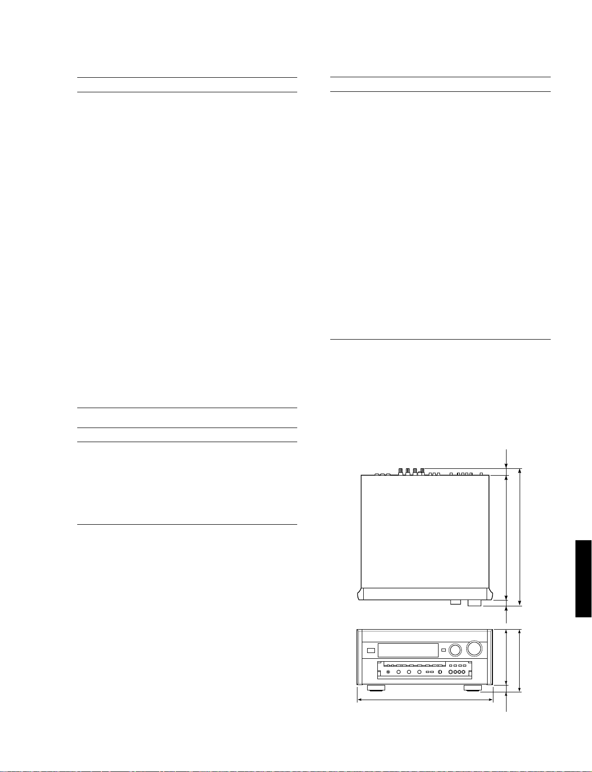
Dimensions (W x H x D) . . . . . . . . . . . 471 x 211.5 x 473mm
(18-9/16” x 8-5/16” x 18-5/8”)
Weight . . . . . . . . . . . . . . . . . . . . . . . . . .28.0 kg (61 lbs 11oz)
Finish
RX-V1 . . . . . . . . . . . . . . . . . . . . . . . Gold color/Black color
DSP-AX1 . . . . . . . . . . . . . . . . . . . . Gold color/Black color
Accessories
RX-V1 only . . . . . . . . . . . . . . . . . . . AM loop antenna x 1
Indoor FM antenna x 1
DSP-AX1/RX-V1 . . . . . . . Remote Control Transmitter x 1
Battery (size "AA", "R06") x 3
* Specifications subject to change without notice.
U . . . . . . . . . . USA model
C . . . . . . Canadian model
A . . . . . Australian model
B . . . . . . . . British model
G . . . . . European model
R . . . . . . . General model
T . . . . . . . . . China model
Tuning Range
U, C models . . . . . . . . . . . . . . . . . . . . . . . .530 to 1,710kHz
A model . . . . . . . . . . . . . . . . . . . . . . . . . . .531 to 1,611kHz
Usable Sensitivity . . . . . . . . . . . . . . . . . . . . . . . . . . 300µV/m
Output Level
AM 30% mod. 1kHz . . . . . . . . . . . . . . . . . . . . . . . . 150mV
Signal-to-Noise Ratio . . . . . . . . . . . . . . . . . . . . . . . . . . 52dB
Antenna . . . . . . . . . . . . . . . . . . . . . . . . . . . . . . . Loop antenna
Manufactured under license from Dolby Laboratories.
"Dolby", "AC-3", "Pro Logic", and the double-D symbol V
are trademarks of Dolby Laboratories. © 1992-1997 Dolby
Laboratories. All rights reserved.
Manufactured under license from Digital Theater Systems,
Inc. US Pat. No. 5,451,942 and other world-wide patents
issued and pending. "DTS", "DTS Digital Surround", are
trademarks of Digital Theater Systems, Inc. copyright
1996 Digital Theater Systems, inc. All rights reserved.
● DIMENSIONS
471 (18-9/16")
21.5
(7/8")
429 (16-7/8")
473 (18–5/8")
22.5
(7/8")
190.5 (7-1/2")
211.5 (8–5/16")
21
(13/16")
Units : mm (inch)
DSP-AX1/RX-V1
6
Page 8

DSP-AX1/RX-V1
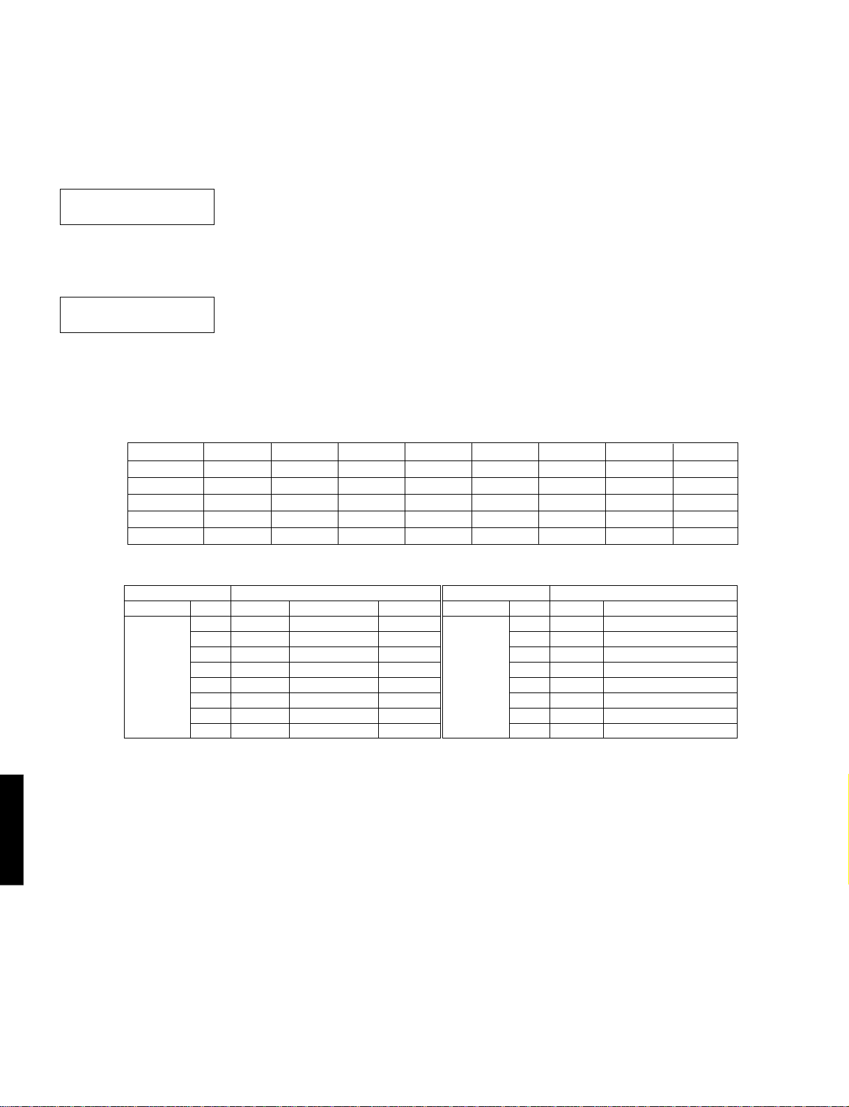
● SET MENU TABLE
No. SET MENU PRESET VALUE SETTING RANGES
1. SPEAKER SET
1A CENTER SPEAKER LARGE LARGE/SMALL/NONE
1B MAIN SPEAKER LARGE LARGE/SMALL
1C REAR L/R SPEAKER LARGE LARGE/SMALL/NONE
1D REAR CT SPEAKER LARGE LARGE/SMALL/NONE
1E LFE/BASS OUT BOTH SUBWOOFER/MAIN/BOTH
1F FRONT EFCT SPEAKER YES YES/NONE
1G MAIN LEVEL NORMAL NORMAL/–10dB
2. LOW FREQ. TEST TONE : OFF ON/OFF
OUTPUT : MAIN L/R L/C/R/RS/RC/LS/SW/FRONT
FREQUENCY : 88Hz 35 — 250Hz
3. DOLBY DIGITAL SET
3A LFE LEVEL SPEAKER : 0dB –20dB — 0dB
HEAD PHONE : 0dB –20dB — 0dB
3B DYNAMIC RANGE SPEAKER : MAX MAX/STD/MIN
HEAD PHONE : MAX MAX/STD/MIN
4. DTS SET
4A LFE LEVEL SPEAKER : 0dB –10dB — +10dB
HEAD PHONE : 0dB –10dB — +10dB
5. SPEAKER DELAY TIME CENTER : 0ms 0ms — 5ms
REAR CENTER : 3ms 0ms — 30ms
6. AUDIO DELAY 0ms 0ms — 99ms
7. CENTER GRAPHIC EQ. EACH ch : 0dB 100Hz — 10kHz, –6dB — +6dB
8. REAR CENTER GRAPHIC EQ. EACH ch : 0dB 100Hz — 10kHz, –6dB — +6dB
9. CINEMA EQ. ALL “OFF”
9A L, C, R EQ. HIGH 12.7kHz, –3dB PEG 12.7kHz, –4dB HIGH, PGE : 1kHz — 12.7kHz
9B FRONT EFCT EQ. HIGH 12.7kHz, 0dB PEG 8kHz, –3dB GAIN : –9dB — +6dB
9C REAR L/R EQ. HIGH 12.7kHz, 0dB PEG 8kHz, –3dB
9D REAR CENTER EQ. HIGH 12.7kHz, 0dB PEG 8kHz, –3dB
10. HP TONE CTRL BASS : 0dB –6dB — +3dB
TREBLE : 0dB –6dB — +3dB
11. PARAMETER INITIALIZE OFF PROGRAM 1 — 12
12. 6.1/ES AUTO ON ON/OFF
13. MEMORY GUARD OFF ON/OFF
14. COMPONENT VIDEO INPUT [A] : DVD
[B] : D-TV
[C] : CBL/SAT
15. INPUT MODE D-TV : AUTO AUTO/LAST
CBL/SAT : AUTO AUTO/LAST
VCR1 : AUTO AUTO/LAST
16. INPUT RENAME LD(Currently selected input)
17. DIMMER 0 –4 — 0
18. ZONE2 SET ZONE2 OUT : FIX FIX/VAR
L, C, R/FRONT EFCT//REAR L,R/REAR CT ON/OFF
DVD, LD, D-TV, CBL/SAT, VCR1, VCR2, VCR3, V-AUX
DVD, LD, D-TV, CBL/SAT, VCR1, VCR2, VCR3, V-AUX
DVD, LD, D-TV, CBL/SAT, VCR1, VCR2, VCR3, V-AUX
● SUPERIMPOSING
DSP-AX1/RX-V1
Input LD, etc. Output Superimposing
Terminal Signal Monitor connection
S O O O (On screen)
VO — X
SO X X
VO — O (On screen)
S O O O (On screen)
VX — X
SO X X
VX — O (Blue back)
SX — X
VO — X (On screen)
SX — O (Blue back)
VX — O (Blue back)
7
S : S video signal
V : Composite video signal
O : YES
X: NO
— : NO CARE
Caution: Superimposing function is not usable for component signals.
Page 9
Sub-program
Name
[ SP MODE ]
Europe Hall A
Europe Hall B
Europe Hall C
U.S.A. Hall D
Europe Hall E
Live Concert
Tokyo
Freiburg
Royaumont
Village Gate
Village Vanguard
The Bottom Line
Roxy Theatre
Warehouse Loft
Arena
Disco
Party
Game/Amusement
Pop/Rock
DJ
Classical/Opera
Pavilion
Mono Movie
Variety/Sports
Spectacle
Sci-Fi
Adventure
General
Normal
Enhanced
(P.)INIT.DLY
ms
30
30
30
35
30
45
40
95
69
21
26
30
15
15
15
26
15
45
21
23
28
23
49
10
13
16
15
15
(P.)ROOM
SIZE
1.0
1.0
1.0
1.0
1.0
1.0
1.0
1.0
1.0
1.0
1.0
1.0
1.0
1.0
1.0
1.0
1.0
1.0
1.0
1.0
1.0
1.0
(P.)LIVENESS
5
5
5
5
5
5
3
3
3
3
5
5
5
5
7
5
5
5
2
S.DELAY
(2ch) ms
25
30
30
30
30
23
20
20
20
20
20
S.DELAY
(DD/dts) ms
10
5
5
5
5
5
15
15
15
5
5
5
7
8
8
12
12
12
5
5
5
5
8
8
15
15
15
15
5
5
S.INIT.DLY
(DD/dts) ms
31
31
31
20
12
32
2
12
23
19
S.INIT.DLY
(DD+EX/dts+ES) ms
31
31
31
20
12
32
2
12
23
19
S.ROOM SIZE
(2ch)
1.0
1.0
1.0
1.0
1.0
1.0
1.0
1.0
1.0
1.0
S.ROOM SIZE
(DD/dts)
1.0
1.0
1.0
1.0
1.0
1.0
1.0
1.0
1.0
1.0
S.ROOM SIZE
(DD+EX/dts+ES)
1.0
1.0
1.0
1.0
1.0
1.0
1.0
1.0
1.0
1.0
S.LIVENESS
(2ch)
4
S.LIVENESS
(DD/dts)
4
S.LIVENESS
(DD+EX/dts+ES)
4
RC.INIT.DLY
ms
15
15
15
15
15
15
15
15
15
15
RC.ROOM
SIZE
1.0
1.0
1.0
1.0
1.0
1.0
1.0
1.0
1.0
1.0
RC.LIVENESS
5
REV.TIME
s
2.5
4.0
4.0
1.6
2.0
2.0
2.7
2.5
2.5
2.2
2.5
2.5
1.6
REV.DELAY
ms
122
130
120
100
160
120
120
140
130
120
142
160
100
REV.LEVEL
%
56
55
52
7
6
8
4
4
10
1
4
2
4
EFCT TRIM
db
0
0
0
0
0
0
0
0
0
0
0
0
0
0
0
0
0
0
0
0
0
0
0
0
0
0
0
0
Sub-program
Name
[ HP MODE ]
Europe Hall A
Europe Hall B
Europe Hall C
U.S.A. Hall D
Europe Hall E
Live Concert
Tokyo
Freiburg
Royaumont
Village Gate
Village Vanguard
The Bottom Line
Roxy Theatre
Warehouse Loft
Arena
Disco
Party
Game/Amusement
Pop/Rock
DJ
Classical/Opera
Pavilion
Mono Movie
Variety/Sports
Spectacle
Sci-Fi
Adventure
General
Normal
Enhanced
(P.)INIT.DLY
ms
30
32
30
35
30
45
40
95
69
21
26
30
15
15
28
26
15
45
21
23
28
23
45
10
13
21
16
15
(P.)ROOM
SIZE
1.0
1.0
1.0
1.0
1.0
1.0
1.0
1.0
1.0
1.0
1.0
1.0
1.0
1.0
1.0
1.0
1.0
1.0
1.0
1.0
1.0
1.0
(P.)LIVENESS
5
5
5
5
5
5
3
3
3
3
5
5
5
5
7
5
5
5
2
S.DELAY
(2ch) ms
25
30
30
30
30
23
20
20
20
20
20
S.DELAY
(DD/dts) ms
10
5
5
5
5
5
15
15
15
5
5
5
7
8
8
12
12
12
5
5
5
5
8
8
8
8
8
15
5
5
S.INIT.DLY
(DD/dts) ms
31
30
18
20
12
32
16
32
23
19
S.INIT.DLY
(DD+EX/dts+ES) ms
31
30
18
20
12
32
16
12
23
19
S.ROOM SIZE
(2ch)
1.0
1.0
1.0
1.0
1.0
1.0
1.0
1.0
1.0
1.0
S.ROOM SIZE
(DD/dts)
1.0
1.0
1.0
1.0
1.0
1.0
1.0
1.0
1.0
1.0
S.ROOM SIZE
(DD+EX/dts+ES)
1.0
1.0
1.0
1.0
1.0
1.0
1.0
1.0
1.0
1.0
S.LIVENESS
(2ch)
4
S.LIVENESS
(DD/dts)
3
S.LIVENESS
(DD+EX/dts+ES)
3
RC.INIT.DLY
ms
15
15
15
15
15
15
15
15
15
15
RC.ROOM
SIZE
1.0
1.0
1.0
1.0
1.0
1.0
1.0
1.0
1.0
1.0
RC.LIVENESS
5
REV.TIME
s
2.5
4.0
4.0
1.6
2.0
2.0
2.7
2.5
2.5
2.2
2.5
2.5
1.6
REV.DELAY
ms
122
117
120
100
160
120
120
140
110
120
142
160
100
REV.LEVEL
%
56
55
52
7
6
8
4
4
10
2
4
2
4
EFCT TRIM
db
DSP-AX1/RX-V1
PARAMETER TABLE
●
DSP-AX1/RX-V1
8
Page 10
DSP-AX1/RX-V1
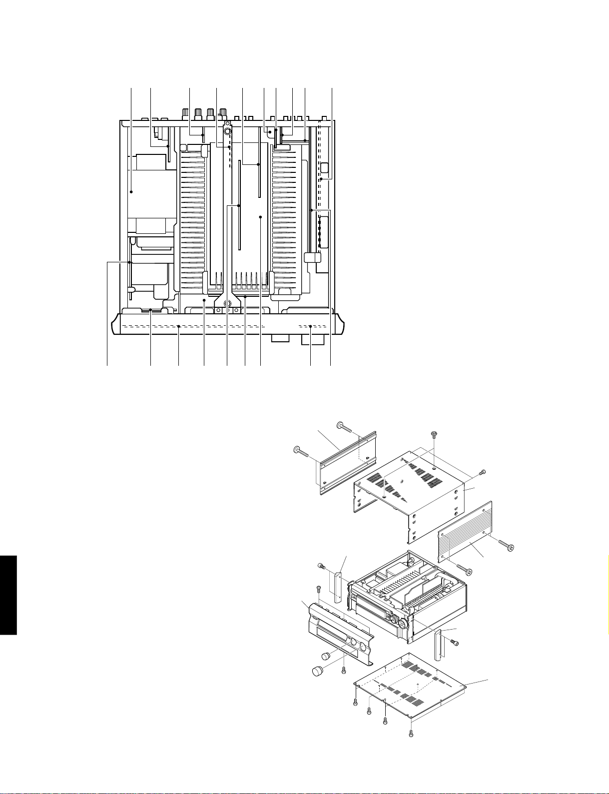
■ INTERNAL VIEW
q u
!1 !5 !9
!2 !3 !8!4 !6 !7
te r y i !0
ow
q POWER TRANSFORMER
w SUB TRANS P. C. B. (1)
e MAIN P. C. B. (4)
r VIDEO P. C. B. (4)
t VIDEO P. C. B. (1)
y SUB TRANS P. C. B. (5)
u SUB TRANS P. C. B. (3)
i VIDEO P. C. B. (2)
o VIDEO P. C. B. (3)
!0 DSP P. C. B. (1)
!1 MAIN P. C. B. (2)
!2 SUB TRANS P. C. B. (4)
!3 DSP P. C. B. (2)
!4 VIDEO P. C. B. (5)
!5 SUB TRANS P. C. B. (2)
!6 MAIN P. C. B. (3)
!7 MAIN P. C. B. (1)
!8 VIDEO P. C. B. (9)
!9 FUNCTION P. C. B. (1)
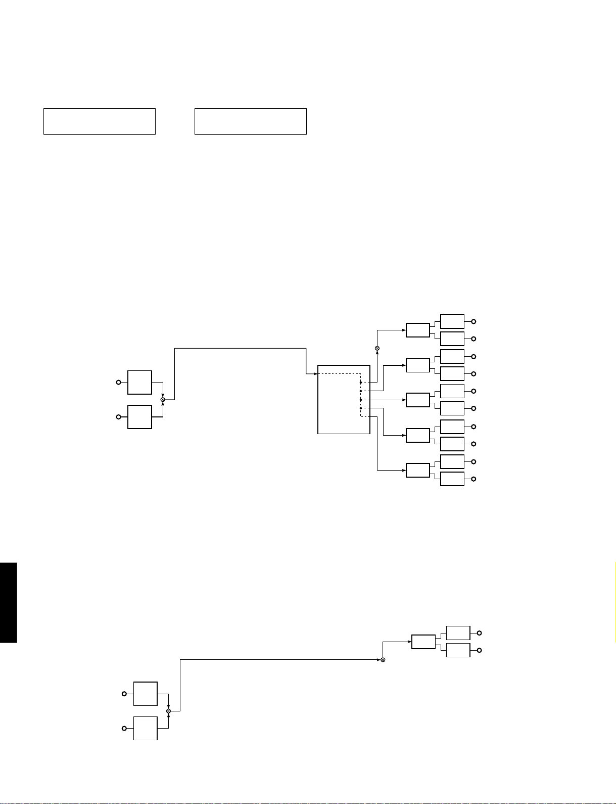
■ DISASSEMBLY PROCEDURES (Remove parts in the order as numbered.)
1. Removal of Top Cover
a. Remove 8 screws ( q ) and then slide the Side Panel
to remove it in Fig. 1.
b. Remove 2 screws ( w ) and 2 screws ( e ) and then
remove the Top Cover in Fig. 1.
2. Removal of Bottom Cover
a. Remove 12 screws ( r ) and then remove the Bottom
Cover in Fig. 1.
3. Removal of Front Panel
a. Remove 2 knobs in Fig. 1.
b. Remove 4 screws ( t ) and then slide the Panel/Side
forward to remove it in Fig. 1.
c. Remove 4 screws (y ) and then remove the Front
Panel in Fig. 1.
DSP-AX1/RX-V1
Side Panel
q
Front Panel
Panel/Side
t
y
q
y
w
e
Top Cover
q
Side Panel
q
Panel/Side
t
Bottom Cover
r
r
r
r
9
Fig. 1
Page 11
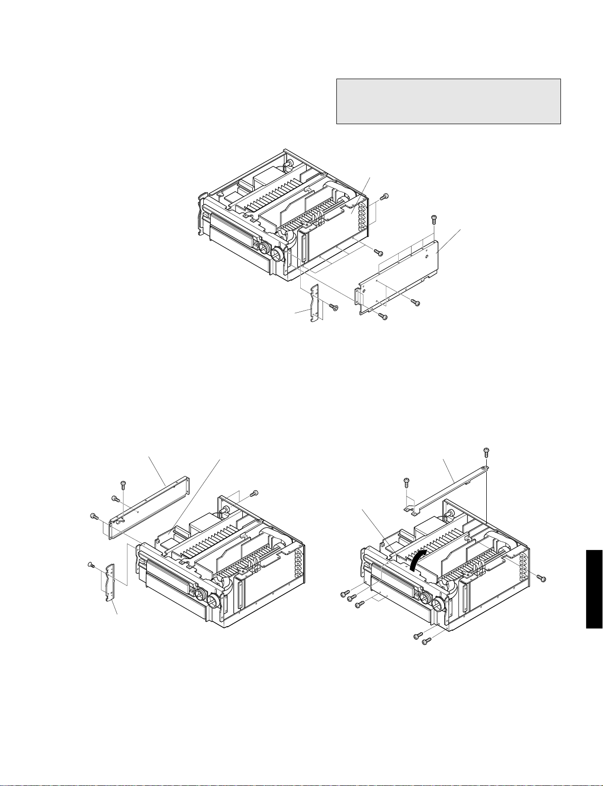
DSP-AX1/RX-V1
4. Removal of DSP P.C.B. (1)
a. Remove 2 screws ( u ) and remove the right Plate
Side in Fig. 2.
b. Remove 15 screws ( i ) and remove the right Upper
Frame in Fig. 2.
Plate Side
(R)
5. Removal of Main P.C.B. (2)
a. Remove 2 screws ( o ) and remove the left Plate
Side in Fig. 3.
a. Remove 6 screws ( !0 ) and then remove the left Side
Frame in Fig. 3.
Note :
1.When the rear panel has been removed, the ground
wire of the input/output pin jack becomes loose.
Connect it to the chassis by using a lead wire.
DSP (1)
i
i
Upper Frame (right)
i
Fig. 2
u
i
i
6. Removal of Main P.C.B. (3)
a. Remove 4 screws ( !1 ) and remove the center Upper
Frame in Fig. 4.
b. Remove 6 screws ( !2 ) and then take up the Sub
Chassis in Fig. 4.
!0
!0
o
Plate Side (L)
Side Frame (L)
!0
MAIN (2)
!1
Upper Frame
(center)
!1
!0
MAIN (3)
DSP-AX1/RX-V1
!1
!2
!2
!2
Fig. 3
!2
!2
Fig. 4
10
Page 12
DSP-AX1/RX-V1
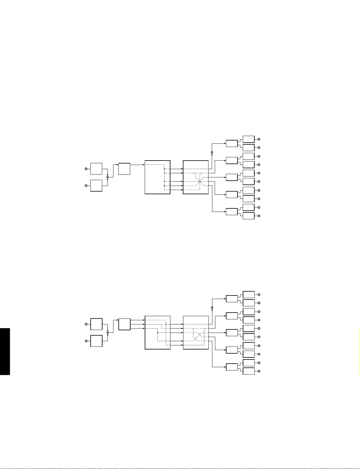
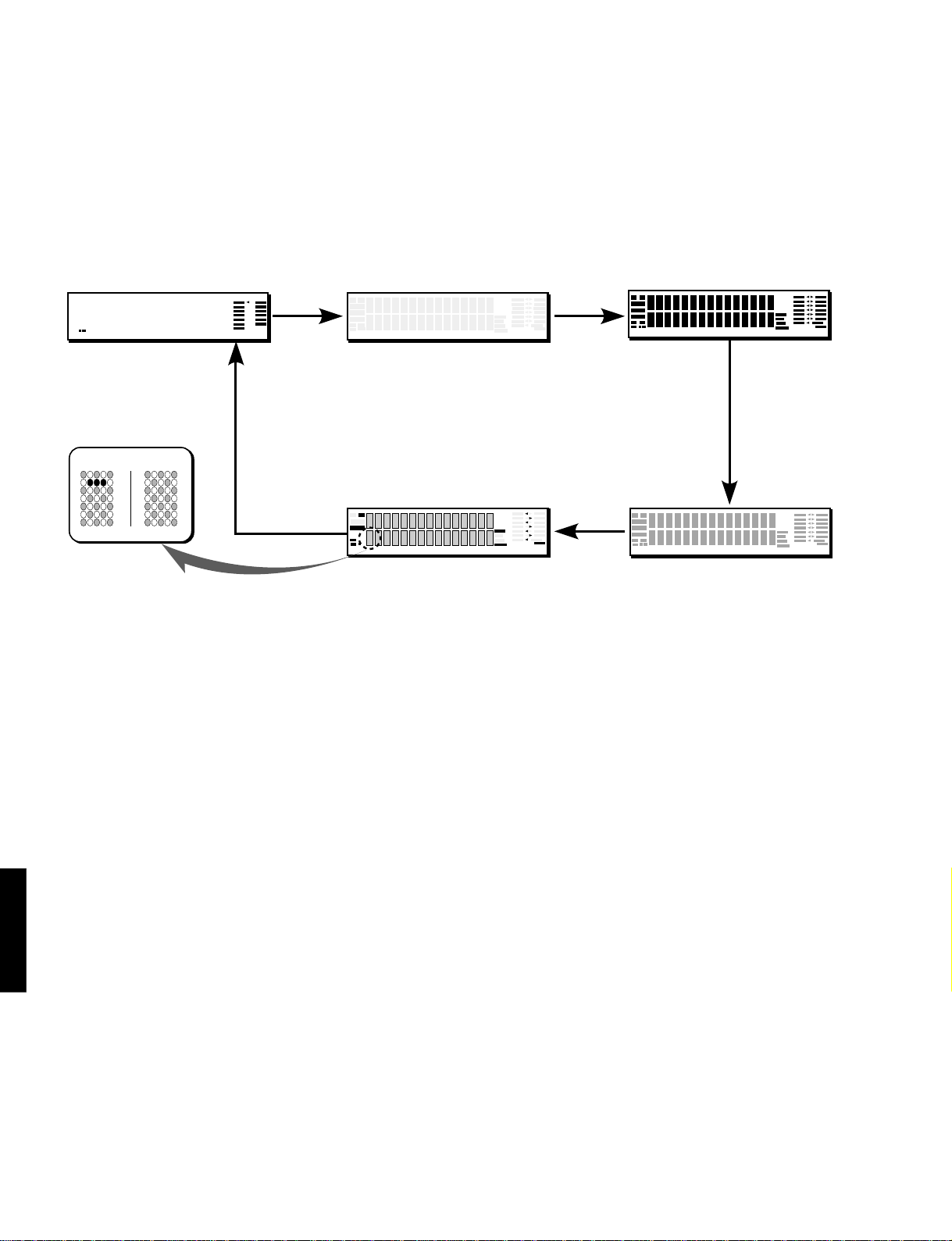
■ SELF DIAGNOSIS FUNCTION
This product has a built-in self diagnosis function (DIAG) to facilitate inspection, measurement and determination of a faulty
item, if any. There are 14 DIAG menu items each of which has sub-menu items.
Listed in the table below are menu items and sub-menu items.
DIAG menu
No.
DSP THROUGH
1
DECODER THROUGH
2
RAM THROUGH
3
PRO LOGIC
4
BYPASS
5
SPEAKERS SET
6
DISPLAY CHECK
7
MANUAL TEST
8
RS-232C
9
PRESET
10
FAN/AD
11
DSP-AX1/RX-V1
IF STATUS (0 – 18)
12
Sub-menu
1. ANALOG BYPASS
2. DSP 0dB
3. DSP FULL BIT
1. YSS918/908
2. DSP FULL BIT
1. 2ch/MULTI
2. DSP FULL BIT
1. YSS918
2. YSS908
3. EFFECT OFF
1. DECODER
2. DSP
1. MAIN:SMALL 0dB
2. MAIN:LARGE -10
3. CENTER:NONE
4. LFE/BASS:MAIN
5. FRONT MIX:5ch
6. CENTER:SMALL
7. REAR:SMALL
1. EFFECT OFF (initial screen)
2. DISPLAY OFF
3. DISPLAY ALL
4. DISPLAY DIMMER (50%)
5. CHECKED PATTERN
1. ALL
2. MAIN L
3. CENTER
4. MAIN R
5. REAR R
6. REAR C
7. REAR L
8. FRONT L
9. FRONT R
10. LFE
1. TX DATA
2. HARD FLOW
1. INHIBIT (memory initialization inhibited)
2. RESERVED (memory initialized)
1. FAN HISTORY
2. KY0, KY1(PANEL KEY)
3. MTR, THM, PRD, PRV
1. SCPU
2. VER
3. SUM
4. CHS1
5. CHS2
6. CHS3
7. CHS4
8. CHS5
9. BSI1
10. BSI2
Remote control code (key)
7A---90 (PRG 9)
7A---91 (PRG 10)
7A---92 (PRG 11)
7A---93 (PRG 12)
7A---10
(TUNER PRESET +)
7A---11
(TUNER PRESET -)
7A---12
(TUNER A/B/C/D/E)
7A---9C (SET DOWN)
7A---9D (SET UP)
7A---9E (SET INC)
7A---9F (SET DEC)
--------7A---88 (PRG 1)
7A---89 (PRG 2)
7A---8A (PRG 3)
7A---8B (PRG 4)
7A---8C (PRG 5)
7A---8D (PRG 6)
7A---8E (PRG 7)
7A---8E (PRG 8)
---------
---------
---------
--------7A---00 (TAPE PLAY)
7A---01 (TAPE RW)
7A---02 (TAPE FW)
7A---03 (TAPE STOP)
7A---04 (TAPE PAUSE)
7A---05 (TAPE MUTE)
7A---06 (TAPE A/B)
7A---07 (TAPE DIR A)
7A---08 (CD PLAY)
7A---09 (CD STOP)
---------
---------
---------
---------
---------
--------7A---56 (EFFECT)
---------
---------
---------
---------
---------
---------
---------
---------
---------
---------
11
Page 13

DSP-AX1/RX-V1
No.
DIAG menu
12
IF STATUS
13
DSP RAM CHECK
14
SUM/VER/PORT
Sub-menu
11. BSI3
12. BSI4
13. BSID
14. DIR5
15. Y918
16. Y908
17. DSP6
18. RAM1
19. RAM2
#1, #2 (DSP RAM check)
1. M, S (main/sub checksum)
2. M, S (main/sub version)
3. PORT (setting confirmation of function setting port)
4. REC-OUT (confirmation of REC OUT port)
Remote control code (key)
---------
---------
---------
---------
---------
---------
---------
---------
---------
---------
---------
---------
---------
---------
● Starting DIAG
For DSP-AX1:
Press the “POWER” (ST ANDBY/ON) key of the main unit while pressing the “SET MENU+” key and the “NEXT” key
located in the sealing panel of the main unit, and DIAG will be activated.
For RX-V1:
Press the “POWER” (ST ANDBY/ON) key of the main unit while pressing the “PROGRAM w” key and the “EFFECT”
key located in the sealing panel of the main unit, and DIAG will be activated.
● Starting DIAG in the protection cancel mode
If the power supply, amplifier protection function is activated and hinders the trouble diagnosis, cancel the protection function as described below, and it will be possible to enter the DIAG mode. (The protection function other than
the excess current detect function will be cancelled.)
For DSP-AX1:
Press the “POWER” (STANDBY/ON) key while pressing the “SET MENU+” key and the “NEXT” key. At this time,
keep pressing the “SET MENU+” key and the “NEXT” for 3 seconds or longer.
For RX-V1:
Press the “POWER” (STANDBY/ON) key while pressing the “PROGRAM w” key and the “EFFECT” key. At this
time, keep pressing the “PROGRAM w” key and the “EFFECT” key for 3 seconds or longer.
In this mode, “ V ” in the FL display of the main unit flashes.
CAUTION!
Using this product with the protection function cancelled may cause damage to itself. Use special care for this point
when using this mode.
● Canceling DIAG
Turn off the power by pressing the “POWER” (STANDBY/ON) key of the main unit or the “STANDBY” key of the
remote control unit.
DSP-AX1/RX-V1
CAUTION: When canceling this function, check that DIAG menu No.10 PRESET (memory initialization inhibited/
reserved) has been set. (To keep the user memory, be sure to select “INHIBIT” (initialization inhibited) from the
No.10 PRESET menu before canceling the DIAG function.)
12
Page 14

DSP-AX1/RX-V1
● Display at the start of DIAG
The diagnostic menu appears on the monitor screen. (It remains on display until it is canceled.)
DIAGNOSTIC MENU
1.DSP THR 8.MAN TST
2.DECODE THR 9.RS232C
3.RAM THR 10.PRESET
4.PRO LOGIC 11.AD DATA
5.DECODE BYP 12.STATUS
6.SP SET 13.DSP RAM
7.E.OFF/DIS 14.SUM/VER
On the FL display of the main unit, an opening message (including the version and the history of
protection function) appears for a few seconds followed by the diagnostic menu display of 1 DSP
THROUGH: ANALOG BYPS.
Opening message
When there is no history
of protection function (*1)
NO PROTECT X/X
M:XXXX / S:XXXX
Checksum of the main
microprocessor
Checksum (4 figures consisting of alphabets and numbers)
The checksum is obtained by adding 4M bits per 1 octo of the entire program code and expressing the result as a
4-figure hexadecimal data. (0xff is added for the area where no code has been entered and for the area other than
ROM code.)
(*1) If the history of the protection function has been recorded, the type of the protection function and
the voltage value recorded last are displayed.
DSP-AX1/RX-V1
Version of the main/sub microprocessor (1 alphabet)
Checksum of the sub
microprocessor
DIAG menu display
1. DSP THROUGH
ANALOG BYPS
13
Page 15

DSP-AX1/RX-V1
In the case where the protection function works after DIAG has been started and the power is turned off ;
When the protection function (*2) works, the history of the protection function appears on display and the power
turns off. Repair the faulty parts according to the displayed history.
(*2) When an excess current or any other faulty condition is found with the power source, DC, etc., the protection
function forces the power to turn off.
I PROTECTION display
I PROTECT X/X
M:XXXX / S:XXXX
PS PRT :000 X/X
M:XXXX / S:XXXX
(When the power is turned on without an abnormality corrected, the protection function works the moment the power relay is turned on to shut off the
power supply.)
Cause: There is an abnormal current flow to the power amplifier.
Supplementary information: If I PROTECTION function has worked after
SP relay ON, a warning message “CHECK SP WIRES” appears the next
time the power is turned on. This indicates that some trouble exists after
the SP terminal, such as a short-circuit of the speaker cable.
PS PRT display
(When the power is turned on without an abnormality corrected, the
protection function works about 1 second later to shut off the power supply.
Display may not be provided, if there is an abnormality with the power
supply for the display.)
Cause: There is an abnormality in the power supply section (voltage).
Supplementary information: As the power from following sources is
detected, it is possible to determine where an abnormality exists.
Transformer secondary winding
VI X 2(CB704), YE x 2(CB482)
U, C only : GY x 2(CB481)
Stabilizing power source
±12, ±5V, +5D1, +5D2, +3.3, VP
DC PRT display
DC PRT :000 X/X
M:XXXX / S:XXXX
TMP PRT:000 X/X
M:XXXX / S:XXXX
Besides the above possible causes, the cause may exist in the disconnected connector or around CPU.
PS PRT, DC PRT and TMP PRT displays include the abnormal A/D value in % (voltage value obtained by considering 5V as 100%). Concerning this value, refer to DIAG menu No.11 FAN/AD described on page 28.
● History of protection function
When the protection function has worked, its history is stored in memory with a backup. Even when no abnormality is noted while
the unit is being serviced, an abnormality which has occurred previously can be defined as long as the backup data has been
stored.
The protection history is cleared when DIAG is canceled by selecting “RESERVED” (memory initialization) from the setting items
of the DIAG menu No.10 PRESET or when the backup data is erased.
(When the power is turned on without an abnormality corrected, the protection function works about 3 seconds later to shut off the power supply.)
Cause: A DC output from the power amplifier is detected in the bad
channel.
TMP PRT display
(When the power is turned on without an abnormality corrected, the protection function works about 3 seconds later to shut off the power supply.)
Cause: The temperature of the heat sinks in the power amplifier is
detected. When the temperature rises and an abnormality is detected, the
power turns off.
DSP-AX1/RX-V1
14
Page 16

DSP-AX1/RX-V1
● Operation procedure of DIAG menu and SUB-MENU
There are No.1 to No.14 MENU items and some SUB-MENU items as well.
DIAG menu selection
DSP-AX1 Main unit: PROGRAM w(forward)/q(reverse) key
RX-V1 Main unit: PRESET TUNING + (forward)/-(reverse) key
SUB-MENU selection
DSP-AX1 Main unit: SET MENU + (forward)/-(reverse) key
RX-V1 Main unit: PROGRAM w(forward)/q(reverse) key
Remote control unit: Only the remote control key in the Menu List can directly call a sub menu.
● Functions during DIAG being set
In addition to the DIAG menu, functions as listed below are available.
• Input selection (including ZONE2), 6CH input
• REC OUT switching
• ZONE2 input, volume
• Front/Center/Rear/Sub-woofer level adjustment
• Muting
• Speaker A/B
• Power on/off operation
• Master volume
It is possible to set to the following volume values using the remote control unit
only during DIAG being set.
Volume value (dB)
• Functions related to the tuner and the set menu are not available.
• It is possible to confirm Menu No.12 IF STA TUS while keeping the signal process (operation status)
of each DIAG menu by using the INPUT MODE key of the main unit.
● Initial settings used to start DIAG function
Following initial settings are used when starting the DIAG function.
When the DIAG function is canceled, the settings before starting DIAG will be restored.
• Input, ZONE2 input: LD (6CH INPUT OFF)
• Master volume: -40dB
• ZONE2 volume: -6dB
• Front/Center/Rear/Sub-woofer level: 0dB
• Audio mute: OFF
• Speaker A/B: ON
DSP-AX1/RX-V1
0
-21
-35
MUTE
Remove control code (key)
7A---E0 (PAGE A)
7A---E1 (PAGE B)
7A---E2 (PAGE C)
7A---E3 (PAGE D)
15
Page 17

DSP-AX1/RX-V1
1. DSP THROUGH
FULL BIT
Details of DIAG menu
In each menu, “SPEAKERS” is always set to “LARGE”, D-RANGE to “MAX”, LFE LEVEL to 0dB (-10dB when
DOLBY DIGITAL is used) and CENTER DELAY to 0ms unless otherwise specified.
1. DSP THROUGH
There are 3 sub menu items (ANALOG BYPS, DSP 0dB, FULL BIT).
1. DSP THROUGH
ANALOG BYPS
IC3
ANALOG
A/D
AK5383
1. DSP THROUGH
DSP 0dB
ANALOG BYPS [Remote control code: 7A—90(PRG 9)]
• The input mode is fixed to use the analog (A/D) system.
• The L/R signal is output through the analog bypass without using the DSP section.
• C/RC, RL/RR, FL/FR, SWL/SWR signals are output using L/R through via DSP.
L
R
IC4
IC6
AC3D2av
YSS918
PCM THR
L/R
IC7 IC8
DSP6#1 YSS910
RLef : RL EFFECT
RRef : RR EFFECT
ZERO : Digital 0
C/LFE
RLef/RRef
FL/FR
RC/ZERO
DSP6#2 YSS910
RC
LFE
C/RC
FL/FR
RL/RR
SWL/SWR
FILTER
DF1704
FILTER
DF1704
FILTER
DF1704
FILTER
DF1704
D/A
PCM1704
D/A
PCM1704
D/A
PCM1704
D/A
PCM1704
D/A
PCM1704
D/A
PCM1704
D/A
PCM1704
D/A
PCM1704
C
RC
FL
FR
RL
RR
SWL
SWR
AC3D2av outputs signals using 2ch though. (L/F)
• DSP6#1 outputs the L/R input signals to C/LFE (SD61 1), RLef/RRef (SD613), FL/FR (SD614),
RC (SD615, L only).
• DSP6#2 outputs the output signals from DSP6#1 to C/RC (SD621), RL/RR (SD623), FL/FR
(SD622), SWL/SWR (SD624).
Note: (SDxxx) represents a terminal name of DSP6#1 and DSP6#2.
Reference
CD ANALOG IN : – 20dBV, Both ch
VOLUME : MAX
PRE OUT
MAIN L (1kHz) : – 3.7dBV
MAIN R (1kHz) : – 3.7dBV
CENTER (1kHz) : – 3.2dBV
REAR CENTER (1kHz) : – 3.4dBV
FRONT L (1kHz) : – 3.5dBV
FRONT R (1kHz) : – 3.4dBV
REAR L (1kHz) : – 3.4dBV
REAR R (1kHz) : – 3.3dBV
SW L (50Hz) : – 3.3dBV
SW R (50Hz) : – 3.3dBV
SW MONO (50Hz) : + 2.7dBV
DSP-AX1/RX-V1
16
Page 18
DSP-AX1/RX-V1
DSP 0dB [Remote control code: 7A—91 (PRG 10)]
The input signal is automatically identified and switched in the priority order of dts > DOLBY DIGITAL > PCM
AUDIO > Analog (A/D) according to the signal detection.
The L/R, C/LFE, FL/FR, RL/RR, RC signals are output through DSP.
(In the case of 2-ch source)
• AC3D2av outputs signals using 2ch though. (L/R)
• DSP6#1 outputs the L/R input signals to L/R (SD610), C/LFE (SD611), RLef/RRef (SD613), FL/FR (SD614), RC
(SD615, L only).
• DSP6#2 outputs the output signals of DSP6#1 to L/R (SD620), C/RC (SD621), RL/RR (SD623), FL/FR (SD622),
SWL/SWR (SD624).
Reference
(In the case of multi-ch source)
• AC3D2av outputs signals using DOLBY DIGITAL/dts decode operation.
• DSP6#1 outputs the L/R input signals to L/R (SD610), RC (SD615, L only), C/LFE to C/LFE (SD611),
LSt/RSt to RLdr/RRdr (SD612), FL/FR (SD614) respectively.
• DSP6#2 outputs the output signals of DSP6#1 to L/R (SD620), C/RC (SD621), RL/RR (SD623), FL/
FR (SD622), SWL/SWR (SD624).
Reference
DSP-AX1/RX-V1
CD ANALOG IN : – 20dBV, Both ch
VOLUME : MAX
PRE OUT
MAIN L (1kHz) : – 3.5dBV
MAIN R (1kHz) : – 3.5dBV
CENTER (1kHz) : – 3.2dBV
REAR CENTER (1kHz) : – 3.4dBV
FRONT L (1kHz) : – 3.5dBV
FRONT R (1kHz) : – 3.4dBV
IC6
L/R
AC3D2av
YSS918
PCM THR
IC4
DIGITAL
ANALOG
IC2
DIR5
YSD917
IC3
A/D
AK5383
CD DIGITAL IN : 1kHz, – 20dBV
VOLUME : MAX
PRE OUT
MAIN L : + 4.2dBV
MAIN R : + 4.2dBV
CENTER : + 4.5dBV
REAR CENTER : + 4.2dBV
IC6
L/R
AC3D2av
C/LFE
YSS918
DD/dts
LSt/RSt
DECODE
IC4
DIGITAL
ANALOG
IC2
DIR5
YSD917
IC3
A/D
AK5383
REAR L (1kHz) : – 3.4dBV
REAR R (1kHz) : – 3.4dBV
SW L (50Hz) : – 3.4dBV
SW R (50Hz) : – 3.4dBV
SW MONO (50Hz) : + 2.7dBV
IC7 IC8
DSP6#1 YSS910
L/R
C/LFE
RLef/RRef
FL/FR
RC/ZERO
DSP6#2 YSS910
LFE
RLdr : RL DIRECT
RRdr : RR DIRECT
FRONT L : + 4.2dBV
FRONT R : + 4.3dBV
REAR L : + 4.3dBV
REAR R : + 4.3dBV
IC7 IC8
DSP6#1 YSS910
L/R
C/LFE
RLdr/RRdr
FL/FR
RC/ZERO
DSP6#2 YSS910
LFE
FILTER
DF1704
FILTER
DF1704
FILTER
DF1704
FILTER
DF1704
FILTER
DF1704
FILTER
DF1704
FILTER
DF1704
FILTER
DF1704
FILTER
DF1704
FILTER
DF1704
PCM1704
D/A
PCM1704
D/A
PCM1704
D/A
PCM1704
D/A
PCM1704
D/A
PCM1704
D/A
PCM1704
D/A
PCM1704
D/A
PCM1704
D/A
PCM1704
D/A
PCM1704
D/A
PCM1704
D/A
PCM1704
D/A
PCM1704
D/A
PCM1704
D/A
PCM1704
D/A
PCM1704
D/A
PCM1704
D/A
PCM1704
D/A
PCM1704
R
C
RC
FL
FR
RL
RR
SWL
SWR
L
R
C
RC
FL
FR
RL
RR
SWL
SWR
L/R
IC57
C/RC
RC
FL/FR
RL/RR
SWL/SWR
L/R
IC57
C/RC
RC
FL/FR
RL/RR
SWL/SWR
D/A
L
FULL BIT [Remote control code: 7A—92 (PRG11)]
The head margin is unused and the digital data is output in full bit.
The same applies as “DSP 0dB” except that the digital data is output in full bit at D/A.
Reference
CD ANALOG IN : – 30dBV, Both ch
VOLUME : MAX
PRE OUT
MAIN L (1kHz) : – 7.5dBV
MAIN R (1kHz) : – 7.5dBV
CENTER (1kHz) : – 7.2dBV
REAR CENTER (1kHz) : – 7.5dBV
FRONT L (1kHz) : – 7.5dBV
FRONT R (1kHz) : – 7.5dBV
REAR L (1kHz) : – 1.4dBV
REAR R (1kHz) : – 1.4dBV
SW L (50Hz) : + 7.5dBV
SW R (50Hz) : + 7.5dBV
SW MONO (50Hz) : + 13.5dBV
17
Page 19

2. DECODER THR.
The input signal is automatically identified and switched in the priority order of dts > DOLBY DIGITAL
> PCM AUDIO > Analog (A/D). There are two sub-menu items (YSS918/908, FULL BIT). This menu is
used to check the signal passage of the decoder LSI (YSS918, YSS908).
DSP-AX1/RX-V1
2. DECODER THR.
YSS918/908
2. DECODER THR.
FULL BIT
YSS918/908 [Remote control code: 7A—93 (PRG12)]
(In the case of 2-ch source)
• AC3D2av outputs L/R input signals from L/R (SDA200, Lt/Rt (SDA21) and C/LFE (SDA22).
• AC3D2av outputs the Lt/Rt output signals of AC3D2av from LS/RS (SDA10).
• DSP6#1 outputs the L/R input signals to L/R (SD610) and RC (SD615, L only), C/LFE (SD611) input
signals to C/LFE (SD611), Lt/Rt input signals to FL/FR (SD614) and LS/RS input signals to RLdr/
RRdr (SD612) respectively.
• DSP6#2 outputs the output signals of DSP6#1 to L/R (SD620), C/RC (SD621), RL/RR (SD623), FL/
FR (SD622) and SWL/SWR (SD624).
Note: (SDAxx) represents the terminal name of AC3Dav and AC3D2av.
(SDxxx) represents the terminal name of DSP6#1 and DSP6#2.
Reference
CD ANALOG IN : – 20dBV, Both ch
VOLUME : MAX
PRE OUT
MAIN L (1kHz) : – 3.5dBV
MAIN R (1kHz) : – 3.4dBV
CENTER (1kHz) : – 3.2dBV
REAR CENTER (1kHz) : – 3.4dBV
FRONT L (1kHz) : – 3.5dBV
FRONT R (1kHz) : – 3.4dBV
IC6
L/R
AC3D2av
C/LFE
YSS918
Lt/Rt
PCM THR
Lt/Rt
IC4
AC3Dav
YSS908
DD/dts
DECODE
IC5
LS/RS
DIGITAL
ANALOG
IC2
DIR5
YSD917
IC3
A/D
AK5383
REAR L (1kHz) : – 3.4dBV
REAR R (1kHz) : – 3.3dBV
SW L (50Hz) : – 3.3dBV
SW R (50Hz) : – 3.3dBV
SW MONO (50Hz) : + 2.7dBV
IC7 IC8
DSP6#1 YSS910
L/R
C/LFE
RLdr/RRdr
FL/FR
RC/ZERO
DSP6#2 YSS910
LFE
FILTER
DF1704
FILTER
DF1704
FILTER
DF1704
FILTER
DF1704
FILTER
DF1704
PCM1704
D/A
PCM1704
D/A
PCM1704
D/A
PCM1704
D/A
PCM1704
D/A
PCM1704
D/A
PCM1704
D/A
PCM1704
D/A
PCM1704
D/A
PCM1704
L/R
IC57
C/RC
RC
FL/FR
RL/RR
SWL/SWR
D/A
(In the case of multi-ch source)
• AC3D2av outputs dts or DOLBY DIGITAL encoded input signals from Lt/Rt (SDA21) without decoding.
• AC3Dav processes Lt/Rt output signals of AC3D2av by dts or DOLBY DIGITAL decoding and outputs them to LS/RS (SDA10) and RC (SDA12, L only) through 3/0 down-mixing.
• DSP6#1 outputs the LS/RS input signals to RLdr/RRdr (SD612) and the RC (L only) input signals to
RC (SD615, L only).
• DSP6#2 outputs the output signals of DSP6#1 to RC (SD621, R only) and RL/RR (SD623).
L
R
C
RC
FL
FR
RL
RR
SWL
SWR
DSP-AX1/RX-V1
Reference
CD DIGITAL IN : 1kHz, – 20dBV
VOLUME : MAX
PRE OUT
MAIN L : + 4.5dBV
MAIN R : + 4.6dBV
CENTER : + 4.9dBV
REAR CENTER : + 4.6dBV
IC6
AC3D2av
YSS918
PCM THR
IC4
AC3Dav
YSS908
DD/dts
DECODE
IC5
DIGITAL
ANALOG
IC2
DIR5
YSD917
IC3
A/D
AK5383
FRONT L : + 4.6dBV
FRONT R : + 4.6dBV
REAR L : + 4.7dBV
REAR R : + 4.7dBV
DSP6#1 YSS910
Lt/Rt
Lt/Rt
LS/RS
RC/ZERO
IC7 IC8
DSP6#2 YSS910
RLdr/RRdr
RC/ZERO
RC
FILTER
DF1704
RC
RL/RR
FILTER
DF1704
D/A
PCM1704
D/A
PCM1704
D/A
PCM1704
RC
RL
RR
18
Page 20

DSP-AX1/RX-V1
FULL BIT [Remote control code: 7A—10 (TUNER PRESET +)]
The head margin is unused and the digital data is output in full bit.
The same applies as YSS918/908 except that the digital data is output in full bit at D/A.
Reference
CD ANALOG IN : – 30dBV, Both ch
VOLUME : MAX
PRE OUT
MAIN L (1kHz) : – 7.5dBV
MAIN R (1kHz) : – 7.5dBV
CENTER (1kHz) : – 7.2dBV
REAR CENTER (1kHz) : – 7.5dBV
FRONT L (1kHz) : – 7.5dBV
FRONT R (1kHz) : – 7.4dBV
REAR L (1kHz) : – 1.4dBV
REAR R (1kHz) : – 1.3dBV
SW L (50Hz) : + 7.6dBV
SW R (50Hz) : + 7.5dBV
SW MONO (50Hz) : + 13.7dBV
3. RAM THROUGH
The input data is automatically identified and switched in the priority order of dts > DOLBY DIGITAL >
PCM AUDIO > Analog (A/D) according to the signal detection.
The main L/R uses the analog through method when analog signals are input and the DSP through
method when digital signals are input.
There are two sub-menu items (2ch/MULTI, FULL BIT).
3. RAM THROUGH
2ch/MULTI
2ch/MULTI [Remote control code: 7A—11 (TUNER PRESET -)]
(In the case of 2-ch source)
• AC3D2av outputs signals using 2ch though. (L/R)
• DSP6#1 outputs the L/R input signals to L/R (SD610), C/LFE (SD61 1) and RC (SD615, L only). Also,
it outputs L/2 + R/2 to RLef/RRef (SD613) and FL/FR (SD614) through the external RAM.
• DSP6#2 outputs the output signals of DSP6#1 to L/R (SD620), RL/RR (SD623), FL/FR (SD622),
SWL/SWR (SD624). Also, it outputs C/RC to C/RC (SD621) through the external RAM.
3. RAM THROUGH
FULL BIT
Reference
DIGITAL
ANALOG
DSP-AX1/RX-V1
CD ANALOG IN : – 20dBV, Both ch
VOLUME : MAX
PRE OUT
MAIN L (1kHz) : – 3.5dBV
MAIN R (1kHz) : – 3.4dBV
CENTER (1kHz) : – 3.2dBV
REAR CENTER (1kHz) : – 3.4dBV
FRONT L (1kHz) : – 3.4dBV
FRONT R (1kHz) : – 3.4dBV
IC4
IC6
AC3D2av
YSS918
PCM THR
L/R
IC2
DIR5
YSD917
IC3
A/D
AK5383
REAR L (1kHz) : – 3.4dBV
REAR R (1kHz) : – 3.3dBV
SW L (50Hz) : – 3.3dBV
SW R (50Hz) : – 3.3dBV
SW MONO (50Hz) : + 2.7dBV
IC7 IC8
DSP6#1 YSS910
4M DRAM
IC33
IC34
L/R
C/LFE
RLef/RRef
FL/FR
L/2
+
R/2
RC/ZERO
DSP6#2 YSS910
LFE
IC35
C/RC
4M DRAM
L/R
IC57
C/RC
FL/FR
RL/RR
SWL/SWR
FILTER
DF1704
FILTER
DF1704
FILTER
DF1704
FILTER
DF1704
FILTER
DF1704
D/A
PCM1704
D/A
PCM1704
D/A
PCM1704
D/A
PCM1704
D/A
PCM1704
D/A
PCM1704
D/A
PCM1704
D/A
PCM1704
D/A
PCM1704
D/A
PCM1704
L
R
C
RC
FL
FR
RL
RR
SWL
SWR
19
Page 21
(In the case of multi-ch source)
• AC3D2av outputs signals using DOLBY DIGITAL/dts decode operation.
• DSP6#1 outputs the L/R signals to L/R (SD610), RC (SD615, L only), C/LFE to C/LFE (SD611), LSt/
RSt to RLdr/RRdr (SD612). Also, it outputs L/2 + R/2 to FL/FR (SD614) through the external RAM.
• DSP6#2 outputs the output signals of DSP6#1 to L/R (SD620), FL/FR (SD622), SWL/SWR (SD624).
Also, it outputs C/RC and RL/RR to C/RC (SD621) and RL/RR (SD623) through the external RAM.
DSP-AX1/RX-V1
Reference
CD DIGITAL IN : 1kHz, – 20dBV
VOLUME : MAX
PRE OUT
MAIN L : + 4.2dBV
MAIN R : + 4.2dBV
CENTER : + 4.5dBV
REAR L : + 4.3dBV
REAR R : + 4.3dBV
REAR CENTER : + 4.2dBV
DIGITAL
ANALOG
FRONT L : + 4.2dBV
FRONT R : + 4.3dBV
IC4
IC6
AC3D2av
YSS918
DD/dts
DECODE
IC2
DIR5
YSD917
IC3
A/D
AK5383
LSt : LS total
RSt : RS total
L/R
C/LFE
LSt/RSt
IC7 IC8
DSP6#1 YSS910
L/R
C/LFE LFE
RLdr/RRdr
FL/FR
RC/ZERO
IC33
IC34
L/2+R/2
4M DRAM
DSP6#2 YSS910
C/RC
RL/RR
IC35
4M DRAM
L/R
IC57
C/RC
FL/FR
RL/RR
SWL/SWR
FULL BIT [Remote control code: 7A—92 (TUNER A/B/C/D/E)]
The head margin is unused and the digital data is output in full bit.
The same applies as “2ch/MULTI” 0dB” except that the digital data is output in full bit at D/A.
FILTER
DF1704
FILTER
DF1704
FILTER
DF1704
FILTER
DF1704
FILTER
DF1704
D/A
PCM1704
D/A
PCM1704
D/A
PCM1704
D/A
PCM1704
D/A
PCM1704
D/A
PCM1704
D/A
PCM1704
D/A
PCM1704
D/A
PCM1704
D/A
PCM1704
L
R
C
RC
FL
FR
RL
RR
SWL
SWR
Reference
CD ANALOG IN : – 30dBV, Both ch
VOLUME : MAX
PRE OUT
MAIN L (1kHz) : – 7.5dBV
MAIN R (1kHz) : – 7.5dBV
CENTER (1kHz) : – 7.2dBV
REAR CENTER (1kHz) : – 7.4dBV
FRONT L (1kHz) : – 7.5dBV
FRONT R (1kHz) : – 7.4dBV
REAR L (1kHz) : – 1.4dBV
REAR R (1kHz) : – 1.3dBV
SW L (50Hz) : + 7.6dBV
SW R (50Hz) : + 7.5dBV
SW MONO (50Hz) : + 13.6dBV
DSP-AX1/RX-V1
20
Page 22
DSP-AX1/RX-V1
4. PRO LOGIC
The input data is automatically identified in the priority order of PCM > Analog. DTS is inhibited.
There are three sub-menu items.
Either Pro-logic (auto input balance turned off ) or EFFECT OFF (analog through) is selected.
4. PRO LOGIC
YSS918
4. PRO LOGIC
YSS908
4. PRO LOGIC
EFFECT OFF
YSS918 [Remote control code: 7A—9C (SET DOWN)]
When the analog, PCM audio or DOLBY DIGITAL 2/0 mode is used, L, R, C, S signals are pro-logic
decoded in YSS918 and output.
When the DOLBY DIGITAL mode other than 2/0 is used, the pro logic function does not work and they
are muted.
(2-ch source) ... Muted in the case of multi-ch source
• AC3D2av outputs signals using PRO LOGIC decoding operation with the auto input balance of f (with
-3dB gain).
• DSP6#1 outputs the PRO LOGIC output signals to L/R (SD610), C(SD611, L only). Also, it passes
the S signal through the external RAM and -3dB processing and outputs it to RLef/RRef (SD613).
• DSP6#2 outputs the output signals of DSP6#1 to L/R (SD620), RL/RR (SD623). Also, it outputs the
C signal to C (SD621, L only) through the external RAM.
L/R
FILTER
DF1704
IC57
RL/RR
C
FILTER
DF1704
FILTER
DF1704
DIGITAL
ANALOG
IC2
DIR5
YSD917
IC3
A/D
AK5383
IC4
IC6
AC3D2av
YSS918
PRO LOGIC
L/R
C/S
IC7 IC8
DSP6#1 YSS910
L/R
CC
RLef/RRef
SC
4M DRAM
IC33
IC34
DSP6#2 YSS910
IC35
4M DRAM
D/A
PCM1704
D/A
PCM1704
D/A
PCM1704
D/A
PCM1704
D/A
PCM1704
L
R
C
RL
RR
Reference
DSP-AX1/RX-V1
21
CD ANALOG IN : – 20dBV, Both ch
VOLUME : MAX
PRE OUT
MAIN L (1kHz) : – 43.0dBV
MAIN R (1kHz) : – 39.0dBV
CENTER (1kHz) : – 0.2dBV
REAR CENTER (1kHz) : – 47.5dBV
FRONT L (1kHz) : – ∞ dBV
FRONT R (1kHz) : – ∞ dBV
REAR L (1kHz) : – ∞ dBV
REAR R (1kHz) : – ∞ dBV
SW L (50Hz) : – ∞ dBV
SW R (50Hz) : – ∞ dBV
SW MONO (50Hz) : – 44.8dBV
CD ANALOG IN : – 20dBV, L ch only
VOLUME : MAX
PRE OUT
MAIN L (1kHz) : – 3.5dBV
MAIN R (1kHz) : – ∞ dBV
CENTER (1kHz) : – 42.4dBV
REAR CENTER (1kHz) : – ∞ dBV
FRONT L (1kHz) : – ∞ dBV
FRONT R (1kHz) : – ∞ dBV
REAR L (1kHz) : – 47.5dBV
REAR R (1kHz) : – 47.5dBV
SW L (50Hz) : – ∞ dBV
SW R (50Hz) : – ∞ dBV
SW MONO (50Hz) : – 44.8dBV
Page 23
YSS908 [Remote control code: 7A—9D (SET UP)]
When the analog, PCM audio or DOLBY DIGITAL 2/0 mode is used, LS, RS, RC signals are pro-logic
decoded in YSS908 and output.
When the DOLBY DIGIT AL mode other than 2/0 is used, the pro logic function does not work and they
are muted.
(2-ch source) ... Muted in the case of multi-ch source
• AC3D2av outputs 2-ch input signals from LSt/RSt (SDA21).
• AC3D2av outputs signals using DOLBY 3 Stereo decoding operation with the auto input balance off
(with -3dB gain).
• DSP6#1 outputs LS/RS to RLdr/RRdr (SD612) and RC to RC (SD615, L only) respectively.
• DSP6#2 outputs the output signals of DSP6#1 to RL/RR (SD623) and RC (SD621, R only) through
the external RAM.
IC7 IC8
DIGITAL
ANALOG
IC2
DIR5
YSD917
IC3
A/D
AK5383
IC4
IC6
AC3D2av
YSS918
PCM THR
LSt/RSt
AC3Dav
YSS908
PRO LOGIC
IC5
DSP6#1 YSS910
LSt/RSt
LS/RS
RC/ZERO
DSP6#2 YSS910
RLdr/RRdr RL/RR
RC/ZERO RC
IC35
4M DRAM
RC
RL/RR
RL/RR
RC
FILTER
DF1704
FILTER
DF1704
DSP-AX1/RX-V1
D/A
D/A
D/A
RC
RL
RR
PCM1704
PCM1704
PCM1704
Reference
CD ANALOG IN : – 20dBV, Both ch
VOLUME : MAX
PRE OUT
MAIN L (1kHz) : – ∞ dBV
MAIN R (1kHz) : – ∞ dBV
CENTER (1kHz/50Hz) : – 0.5dBV/ – 2.0dBV
REAR CENTER (1kHz) : – ∞ dBV
FRONT L (1kHz) : – ∞ dBV
FRONT R (1kHz) : – ∞ dBV
REAR L (1kHz/50Hz) : – 43.1dBV/ – 12.2dBV
REAR R (1kHz/50Hz) : – 38.7dBV/ – 12.1dBV
SW L (50Hz) : – ∞ dBV
SW R (50Hz) : – ∞ dBV
SW MONO (50Hz) : – 45.5dBV
EFFECT OFF [Remote control code: 7A—9E (SET INC)]
• The input mode is fixed to Analog.
• The L/R signal is output through ANALOG MAIN BYP ASS.
IC11
CD ANALOG IN : – 20dBV, L ch only
VOLUME : MAX
PRE OUT
MAIN L (1kHz) : – ∞ dBV
MAIN R (1kHz) : – ∞ dBV
CENTER (1kHz) : – ∞ dBV
REAR CENTER (1kHz/50Hz) : – 42.6dBV/ – 13.6dBV
FRONT L (1kHz) : – ∞ dBV
FRONT R (1kHz) : – ∞ dBV
REAR L (1kHz/50Hz) : – 3.4dBV/ – 5.3dBV
REAR R (1kHz/50Hz) : – ∞ dBV/ – 39.2dBV
SW L (50Hz) : – ∞ dBV
SW R (50Hz) : – ∞ dBV
SW MONO (50Hz) : – 45.5dBV
DSP BLOCK
L
R
DSP-AX1/RX-V1
ANALOG
22
Page 24
DSP-AX1/RX-V1
5. BYPASS
Only PCM and analog modes are used for input signals. The bypassing operation is used according to
the menu setting. There are two sub-menu items (DECODER, DSP). This menu is useful when locating the faulty part by bypassing the decoder LSI and DSP6.
5. BYPASS
DECODER
5. BYPASS
DSP
DECODER [Remote control code: 7A—9F (SET DEC)]
(2-ch source) ... Muted in the case of multi-ch source
• AC3D2av, AC3Dav and DSP6#1 are muted.
• DIR5 or A/D output (SDAT) signals are input directly to DSP6#2 and output to L/R (SD620), C/RC
(SD621), RL/RR (SD623), FL/FR (SD622) and SWL/SWR (SD624).
Reference
CD ANALOG IN : – 20dBV, Both ch
VOLUME : MAX
PRE OUT
MAIN L (1kHz) : – 7.5dBV
MAIN R (1kHz) : – 7.5dBV
CENTER (1kHz) : – 7.2dBV
REAR CENTER (1kHz) : – 7.4dBV
FRONT L (1kHz) : – 7.5dBV
FRONT R (1kHz) : – 7.4dBV
IC2
DIGITAL
ANALOG
DIR5
YSD917
IC3
A/D
AK5383
IC4
REAR L (1kHz) : – 1.4dBV
REAR R (1kHz) : – 1.3dBV
SW L (1kHz/50Hz) : + 7.7dBV/ + 7.5dBV
SW R (1kHz/50Hz) : + 7.7dBV/ + 7.5dBV
SW MONO (1kHz/50Hz) : + 13.8dBV/ + 13.5dBV
L/R (DECODER BYPASS)
IC8
DSP6#2 YSS910
L/R
IC57
C/RC
FL/FR
RL/RR
SWL/SWR
FILTER
DF1704
FILTER
DF1704
FILTER
DF1704
FILTER
DF1704
FILTER
DF1704
D/A
PCM1704
D/A
PCM1704
D/A
PCM1704
D/A
PCM1704
D/A
PCM1704
D/A
PCM1704
D/A
PCM1704
D/A
PCM1704
D/A
PCM1704
D/A
PCM1704
L
R
C
RC
FL
FR
RL
RR
SWL
SWR
DSP [Remote control code: ––––]
(2-ch source) ... Muted in the case of multi-ch source
• AC3D2av, AC3Dav, DSP6#1 and DSP6#2 are muted.
• The DIR5 or A/D output (SDAT) signal is input directly to DAC and L/R is reproduced.
Reference
DSP-AX1/RX-V1
23
CD ANALOG IN : – 20dBV, Both ch
VOLUME : MAX
PRE OUT
MAIN L (1kHz) : – 3.4dBV
MAIN R (1kHz) : – 3.4dBV
CENTER (1kHz) : – ∞ dBV
REAR CENTER (1kHz) : – ∞ dBV
FRONT L (1kHz) : – ∞ dBV
FRONT R (1kHz) : – ∞ dBV
IC2
DIGITAL
ANALOG
DIR5
YSD917
IC3
A/D
AK5383
IC4
REAR L (1kHz) : – ∞ dBV
REAR R (1kHz) : – ∞ dBV
SW L (50Hz) : – ∞ dBV
SW R (50Hz) : – ∞ dBV
SW MONO (50Hz) : – ∞ dBV
L/R (DECODER BYPASS)
IC57
D/A
D/A
L
R
L/R
FILTER
DF1704
PCM1704
PCM1704
Page 25

6. SPEAKERS SET
The input signal is automatically identified in the priority order of dts > DOLBY DIGITAL > PCM >
Analog. There are seven sub-menu items.
The signals output from the DSP are the same as 1. DSP THROUGH: DSP 0dB.
DSP-AX1/RX-V1
[Remote Control Code: 7A—88 (PRG 1)] [Remote Control Code: 7A—89 (PRG 2)]
6. SPEAKERS SET
MAIN:SMALL 0dB
[Remote Control Code: 7A—8B (PRG 4)]
6. SPEAKERS SET
LFE/BASS:MAIN
[Remote Control Code: 7A—8E (PRG 7)]
6. SPEAKERS SET
MAIN:LARGE -10
[Remote Control Code: 7A—8C (PRG 5)]
6. SPEAKERS SET
FRONT MIX:5ch
6. SPEAKERS SET
REAR:SMALL
The analog switch settings for each sub-menu are as shown in the table below.
Sub-menu
1 MAIN : SMALL 0dB
2 MAIN : LARGE -10
3 CENTER : NONE
4 LFE/BASS : MAIN
5 FRONT MIX : 5ch
6 CENTER : SMALL
7 REAR : SMALL
LARGE: Signals are output in all bandwidths.
SMALL: Only signals lower than 90Hz are mixed in the channel specified by LFE/BASS.
NONE: The center contents are distributed to the MAIN L/R channels after -3dB.
CENTER
LARGE
LARGE
NONE
LARGE
LARGE
SMALL
LARGE
REAR
LARGE
LARGE
LARGE
LARGE
LARGE
LARGE
SMALL
MAIN SP
SMALL
LARGE
LARGE
LARGE
LARGE
LARGE
LARGE
MAIN LVL
0dB
-10dB
0dB
0dB
0dB
0dB
0dB
LFE/BASS
SWFR
SWFR
SWFR
MAIN
SWFR
SWFR
SWFR
[Remote Control Code: 7A—8A (PRG 3)]
6. SPEAKERS SET
CENTER:NONE
[Remote Control Code: 7A—8D (PRG 6)]
6. SPEAKERS SET
CENTER:SMALL
FRONT MIX
7ch
7ch
7ch
7ch
5ch
7ch
7ch
Sub-menu
1 MAIN : SMALL 0dB
2 MAIN : LARGE -10
3 CENTER : NONE
4 LFE/BASS : MAIN
5 FRONT MIX : 5ch
6 CENTER : SMALL
7 REAR : SMALL
Application
Confirmation of high/low pass filter characteristic and gain when BASS REDIRECTION is used.
Confirmation of the effects of MAIN LEVEL function
Confirmation of gain of CENTER MIX (Only CENTER contents are output from MAIN L/R.)
Confirmation of gain of BASS MIX (Only LFE/BASS contents are output from MAIN L/R.)
Confirmation of gain of FRONT MIX (Only FRONT contents are output from MAIN L/R.)
Confirmation of high/low pass filter characteristic and gain when BASS REDIRECTION is used.
Confirmation of high/low pass filter characteristic and gain when BASS REDIRECTION is used.
DSP-AX1/RX-V1
24
Page 26
DSP-AX1/RX-V1
7. DISPLAY CHK
This program is used to check lighting of the FL display which changes as shown below according to operation of
the sub-menu.
The signals are processed in the same way as EFFECT OFF of No.4. (The L/R signal is output using ANALOG
MAIN BYPASS setting.)
As for internal/external synchronization switching of super-imposing (image signals), forced external synchronization is selected by the microprocessor control.
[Remote control code: 7A—8E (PRG 8)]
Initial display
7. DISPLAY CHK
EFFECT OFF
Lighting in a lattice
Example of
short
Normal
Segment conditions of the FL driver (IC901, IC902) and the FL tube are checked by turning ON and OFF all
segments. Next, the operation of the FL driver is checked by using the dimmer control. Then a short between
segments next to each other is checked by turning ON and OFF all segments alternately (in a lattice). (In the above
example, the center segment in the second row from the top is shorted.)
[Remote control code: ––––]
All segments OFF
Lighting of segments in a lattice
[Remote control code: ––––]
[Remote control code: ––––]
All segments ON (dimmer 100%)
All segments ON (dimmer 50%)
[Remote control code: ––––]
DSP-AX1/RX-V1
25
Page 27
DSP-AX1/RX-V1
8. MANUAL TEST
The test noise is output by the noise generator with a built-in DSP through the channels specified by the sub-menu.
There are ten sub-menu items.
8. MANUAL TEST
ALL
ALL [Remote control code: 7A—00 (TAPE PLAY)]
Noise is output through all channels.
MAIN L [Remote control code: 7A—01 (TAPE RW)
Noise is output through the MAIN L channel.
CENTER [Remote control code: 7A—02 (TAPE FW)]
Noise is output through the CENTER channel.
MAIN R [Remote control code: 7A—03 (TAPE STOP)]
Noise is output through the MAIN R channel.
REAR R [Remote control code: 7A—04 (TAPE PAUSE)]
Noise is output through the REAR R channel.
REAR C [Remote control code: 7A—05 (TAPE MUTE)]
Noise is output through the REAR CENTER channel.
REAR L [Remote control code: 7A—06 (TAPE A/B)]
Noise is output through the REAR L channel.
FRONT L [Remote control code: 7A—07 (TAPE DIR A)]
Noise is output through the FRONT L channel.
FRONT R [Remote control code: 7A—08 (CD PLAY)]
Noise is output through the FRONT R channel.
LFE [Remote control code: 7A—09 (CD STOP)]
Noise is output through the LFE (sub-woofer) channel.
9. RS-232C
This menu is used to check transmission of the data and the flow port of the hardware.
With the power turned off, short between pins No.2 (RxD) and No.3 (TxD) and between pins No.7
(RTS) and No.8 (CTS) of the RS-232C terminal. (Be sure to turn off the power when shorting pins.)
Start DIAG and select the menu.
There are two sub-menu items.
The signals are processed in the same way as EFFECT OFF under item 4. PRO LOGIC. (The L/R
signals are output using ANALOG MAIN BYPASS.)
RxD
TxD
9. RS-232C
TxD/RxD DATA:XX
9. RS-232C
HARD FLOW :XX
123
6789
TxD/RxD DATA
This sub-menu is used to check transmission of the test data. “OK” appears when the
data is transmitted properly and “NG” when it is not.
In this mode, NULL command transmission is continued after the test command is
transmitted.
HARD FLOW
This sub-menu is used to check operation of the flow port of the hardware. “OK” appears when the check result is satisfactory and “NG” when it is not.
45
RTS CTS
DSP-AX1/RX-V1
26
Page 28
DSP-AX1/RX-V1
10. PRESET
This menu reserves and inhibits initialization of the back-up RAM (parameter, set menu contents, etc. for the sound
field program). The input signals are automatically identified in the priority order of AC-3 > PCM > Analog. The
signals are processed in the same way as EFFECT OFF of No.4.
10. PRESET
INHIBIT
10. PRESET
RESERVED
INHIBIT (Initialization inhibited)
RAM initialization is not executed. Select INHIBIT to protect the values set by the user.
RESERVED
Initialization of the back-up RAM is reserved and it is executed when the power is turned ON
after canceling DIAG. RESERVED should be selected when shipping out of the factory or
resetting RAM.
CAUTION : Before setting to the PRESET RESERVED, write down the existing preset memory content of the Tuner in a
table as shown below. (This is because setting to the PRESET RESERVED will cause the user memory
content to be erased.) (RX-V1 only)
Preset group
A
B
C
D
E
● PRESET STATIONS
STATION FM FACTORY PRESET DATA (MHz)
PAGE NO. U, C, R, T R, T, L, A J
A/C/E 4 98.1 98.1 86.0
P1 P2 P3 P4 P5 P6 P7 P8
STATION AM FACTORY PRESET DATA (kHz)
PAGE NO. U, C, R, T R, T, L, A, J
1 87.5 87.5 76.0
2 90.1 90.1 83.0
3 95.1 95.1 84.0
B/D 4 530 531
5 107.9 108.0 90.0
6 88.1 88.1 78.0
7 106.1 106.1 88.0
8 107.9 108.0 82.1
1 630 630
2 1080 1080
3 1440 1440
5 1710 1611
6 900 900
7 1350 1350
8 1400 1404
DSP-AX1/RX-V1
27
Page 29
DSP-AX1/RX-V1
11. FAN/AD
The sub-menu of this menu displays the A/D conversion value of the main CPU (function circuit board IC27) which
detects the keys and protection functions of the main unit in %. (100% represents 5V.)
It also displays the history of the fan being driven. When in KY0/KY1 page, it is not possible to operate the keys of
the main unit because the values of all keys are detected. But one click on the input selector of the main unit will
cancel this function and sets to the next sub-menu. Clicking there more than once would change the input. If this
has occurred, restore the input being tested. The signal processing state remains the same as that before executing this menu.
11. FAN/AD
FAN HISTORY:000
FAN HISTORY (History of fan being driven)
The voltage value detected from the temperature detect circuit is read by the A/D function of
the microprocessor as a data. Based on that temperature data, the fan driving speed is
controlled in 3 stages. How the fan has been driven is displayed as the history.
bit 2 1 0
000
FAN 3.0V
FAN 3.7V
FAN 5.0V
When there is a history of the fan operation: 1
KY0 KY1
100 100
Standard values of keys (panel keys of the main unit)
DSP-AX1 RX-V1 value
INPUT MODE INPUT MODE 0
PROGRAM q TUNING q 10
PROGRAM w TUNING w 20
— EDIT 30
— FM/AM 40
— MEMORY 50
— TUNING MODE 60
—— 70
—— 80
KEY OFF state KEY OFF state 100
* Selecting “RESERVED” for DIAG menu No.10 and the factory preset
state will clear the history.
KY0/KY1 (Key scanning detect)
KY0/KY1: Panel key of the main unit (10% step)
• When the standard value is deviated by ±4%, KEY A/D fails to function prop-
erly, In this case, check the constant of the partial pressure resistor, soldering
condition, etc.
KY0
Standard
DSP-AX1 RX-V1 value
KY1
EFFECT A/B/C/D/E 0
—— 10
DIAG(*1) DIAG(*2) 20
SET MENU + PROGRAM w 30
NEXT EFFECT 40
6CH INPUT 6CH INPUT 50
SET MENU - PROGRAM q 60
SPEAKERS B SPEAKERS B 70
SPEAKERS A SPEAKERS A 80
KEY OFF state KEY OFF state 100
Standard
MTR THM PRD PRV
0 28 7 10
The above figures are examples for
reference.
(*1) : “SET MENU +” and “NEXT”
(*2) : “PROGRAM w” and “EFFECT”
DSP-AX1/RX-V1
MTR/THM/PRD/PRV [Remote control code: 7A—56 (EFFECT)]
(Detection of the tuner sensitivity , temperature of the heat sink and protection
function)
MTR:Signal sensitivity of the tuner (RX-V1 only)
THM:Detection of the temperature of the heat sink (Normal value: 6~40)
At 5% or less, the protection function works to turn off the power. At
more than 40%, possibility is that there is an error in the temperature
detection system.
PRD: Protection value for DC detection (Normal value: 1~13)
When the value is out of the normal value range, the protection function
works to turn off the power.
PRV: Protection value for power voltage (Normal value: 5~15)
When the value is out of the normal value range, the protection function
works to turn off the power.
28
Page 30

DSP-AX1/RX-V1
12. IF STATUS
Using this menu, the status data is displayed in the hexadecimal notation one after another.
During signal processing, the status before execution of this menu is maintained.
If the input mode is analog fixed in the menu before execution, it is necessary to change it to the digital
mode according to the following procedure.
1) Select either DIAG menu No.2 or No.3 and enter a digital signal.
2) Menu No.12 can be selected by pressing the INPUT MODE key of the main unit. (The input mode
will be fixed to the digital mode.)
There are ten sub-menu items.
The following status information is displayed in the hexadecimal notation according to the sub-menu
operation.
12.IF STATUS 0
SCPU:8503000510
Display
bit 7654 3210
Display bit
DSP-AX1/RX-V1
Example: “E 1” reads as follows.
1110 0001
7654 3210
0
1
2
3
4
5
6
7
8
9
A
B
C
D
E
F
5th byte
4th byte
3rd byte
2nd byte
1st byte
0 0
3210
7654
0000
0001
0010
0011
0100
0101
0110
0111
1000
1001
1010
1011
1100
1101
1110
1111
IF STATUS 0: Indicates the information communicated between sub-microprocessors.
1st byte
Indicates the communication time lag between the main microprocessor and the
sub-microprocessor, malfunction (in display, etc.) caused by a communication error
or some other reason, the input mode selected by the sub-microprocessor to deter
the flickering effect and the head phone state.
bit 7 HEAD PHONE IN
bit 6 0
bit 5 EXT.DECODER IN
bit 4 0
bit 3 From 0000b, PHONO/TUNER/CD/MD/TAPE/DVD/
bit 2 LD/D-TV/CBL-SAT/VCR1/VCR2/VCR3/
bit 1 V-AUX/NONE/there after ERROR
bit 0
2nd byte
Indicates the Fs information of the reproduction signals.
0x00 : analog
0x01 : 32kHz 0x02 : 44.1kHz 0x03 : 48kHz 0x04 : 64kHz 0x05 : 88kHz
0x06 : 96kHz 0x07 : Unknown
Other : Error
3rd byte
Indicates the audio code mode information of the reproduction signals.
0x00 : 1+1 0x01 : 1/0 0x02 : 2/0 0x03 : 3/0 0x04 : 2/1
0x05 : 3/1 0x06 : 2/2 0x07 : 3/2 0x08 : dts7.1
Other : Error
4th byte
Indicates the format information of the reproduction signals.
0x00 : analog (Unlock) 0x01 : Wrong digital (*1)
0x02 : Digital Data 0x03 : IEC1937 Data 0x04 : PCM Audio
0x05 : Dolby Digital 0x06 : D.D.Karaoke 0x07 : D.D.EX
0x08 : RED dts 0x09 : ORANGE dts 0x0A : dts ES
Other : Error
(*1): Digital reproduction cannot be used due to a commercial bit or 4ch audio
reason. So analog reproduction is used.
29
Page 31

DSP-AX1/RX-V1
12.IF STATUS 2
SUM :46423732
12.IF STATUS11
BSI4:000000FF00
12.IF STATUS 7
CHS5:00000000
12.IF STATUS14
Y918:01014180
12.IF STATUS16
DSP6:00000000
12.IF STATUS18
RAM2:4E6F4572
5th byte
Indicates the information on the signal processing status.
bit7 MUTE requested
bit6 dts flashing
bit5 6.1/ES sound field being processed
bit4 RF-DEM mute pin
bit3 MAIN commands all requested
bit2 THROUGH & BYPASS (*2)
bit1 6.1/ES AUTO
bit0 dts analog muted
(*2): In the case of digital signals other than 32kHz, 44.1kHz and 48kHz, through processing is used for
reproducible signals.
IF STATUS 1: Version information of sub-microprocessor
(Asky code)
12.IF STATUS 1
VER.:41323541
IF STATUS 3~7: IEC60958 channel status information of input signals
12.IF STATUS 3
CHS1:0299000299
IF STATUS 8~11: Bit stream information included in the DOLBY DIGITAL
signal (indicated one by one from the 1st byte)
12.IF STATUS 8
BSI1:0000000000
IF STATUS 12: Bit stream information included in the dts
signal
12.IF STATUS12
BSID:FFFFFFFF
IF STATUS 2: Checksum of sub-microprocessor (Asky
code)
IF STATUS 13: Device status information of DIR5 (IC2)
12.IF STATUS13
DIR5:1A418000
IF STATUS 15: Device status information of YSS908 (IC5)
12.IF STATUS15
Y908:00010100
IF STATUS 17: External RAM check status information of
DSP6#1 (IC7)
12.IF STATUS17
RAM1:4E6F4572
IF STATUS 14: Device status information of YSS918 (IC6)
IF STATUS 16: Device status information of DSP6 (IC7,
IC8)
IF ST ATUS 18: External RAM check status information of
DSP6#2 (IC8)
DSP-AX1/RX-V1
30
Page 32

DSP-AX1/RX-V1
13. DSP RAM CHECK
This menu is used to self-diagnose whether or not the external RAM (IC33, 34, 35) and DSP (IC7, 8)
are connected properly, utilizing the CPU -Ext. RAM interface function included in DSP6.
During signal processing, the status before execution of this menu is maintained.
13.DSP RAM CHECK
#1:NoEr #2:NoEr
• Note that a bus error may be indicated also when there is an error with the terminal other than above
buses.
• Detection for the bus check is executed immediately after resetting.
An error which has occurred after starting DIAG cannot be detected.
#1, #2
Checks the address bus and the data bus of DSP#1 (IC7 of DSP circuit board)
and DSP#2 (IC8 of DSP circuit board), and indicates the connection condition.
“NoEr” appears when no error is detected.
When an error is detected in the data bus;
1619 (example): Indicates that there is an incorrect value between bits 16 and
19. If there are two or more incorrect values, priority is placed on the LSB side.
When an error is detected in the address bus;
Ad01 (example): Indicates that the address bit 1 has an error.
Ad17 (example): Indicates that the address bus bit 17 has an error. (With this
product, however, it is possible that A8 and /OE are short-circuited.)
14. SUM/VER /PORT
There are four sub-menu items.
Indicates the checksum, version, port of the main microprocessor (IC27 of the function circuit board)
as well as the checksum and version of the sub-microprocessor (IC1 of the DSP circuit board).
The signals are processed in the same way as EFFECT OFF under item 4. PRO LOGIC. (The L/R
signals are output using ANALOG MAIN BYPASS.)
CAUTION : When replacing the microprocessor, be sure to check the microprocessor compatibility
before replacement. The microprocessor may not be suitable for replacement depending on its communication format. Use of a microprocessor whose communication format is not compatible with the
existing one will cause some communication error between microprocessors.
14.SUM/VER/PORT
M:51F5 / S:A3BB
DSP-AX1/RX-V1
Checksum of sub-microprocessor
(4 figures of alphabets and numbers)
Checksum of main microprocessor
(4 figures of alphabets and numbers)
Checksum of main/sub microprocessor
Checksum: The checksum is obtained by adding 4M bits per 1 octo of the
entire program code and expressing the result as a 4-figure hexadecimal data.
(0xff is added for the area where no code has been entered and for the area
other than ROM code.)
31
Page 33

DSP-AX1/RX-V1
14.SUM/VER/PORT
M:G38DB/ S:E42D
Main microprocessor Sub-microprocessor
M : G 3 8 D B
Software control version (3 figures of alphabet and numbers)
14.SUM/VER/PORT
PORT: 00000000
00000000
Software version/compatible version/RS-232C version of main microprocessor
Software version and compatible version of sub-microprocessor
The alphabet of the compatible version represents the communication format compatibility between the main and sub microprocessors. If the alphabet representing the communication format compatibility agrees, the microprocessors are interchangeable. If
the alphabet is different, the replacement microprocessor will fail to function properly.
RS-232C communication specification
version (1 alphabet)
Compatible version of microprocessor (1 alphabet)
Software control version (3
figures of alphabet and numbers)
S : E 4 2 D
Compatible version of microprocessor (1 alphabet)
Port to check functions of the main microprocessor
Tuner mode 0 (Caution 1)
Tuner mode 1 (Caution 1)
Model type: DSP-AX1 (1) / RX-V1 (0)
ZONE with (1) / without (0)
VIDEO switch: PAL (1) / NTSC (0)
VIDEO format: PAL (1) / NTSC (0)
Head phone: Unconnected (1) / connected (0)
Tuner: Not stereo (1) / stereo (0)
(Caution 1)
Tuner mode 0Tuner mode 1
0 0 AM : 531-1611kHz/9kHz FM : 76.0-90.0MHz/100kHz
0 1 AM : 531-1611kHz/9kHz FM : 87.5-108.0MHz/50kHz
1 0 AM : 530-1710kHz/10kHz FM : 87.5-107.9MHz/200kHz
1 1 DSP-AX1
14.SUM/VER/PORT
REC-OUT:0000
Tuner frequency
Port to check functions of the REC OUT
bit 3 2 1 0
0000
REC OUT bit
3210
PHONO 0111
CD 0110
TUNER 0100
TAPE 0101
MD 0001
DVD 0000
SOURCE 0010
LD 0011
D-TV 1011
CBL/SAT 1010
VCR1 1000
VCR2 1001
VCR3 1101
V-AUX 1100
DSP-AX1/RX-V1
32
Page 34

DSP-AX1/RX-V1
■ AMP ADJUSTMENTS
● IDLING CURRENT ADJUSTMENT
Before this adjustment, wait for 10 minutes with no signal
applied after the power is turned ON.
Item
MAIN L
MAIN R
CENTER
REAR L
REAR R
REAR CENTER
FRONT L
FRONT R
● Test Point
Test Point
CB503
CB504
CB505
CB506
CB507
CB508
CB509
CB510
Adjustment point
CB503
VR504
VR504
VR505
VR506
VR501
VR502
VR503
VR507
VR508
VR505
Rating (DC)
4.0mV to 12.0mV
2.0mV to 6.0mV
4.0mV to 12.0mV
DSP-AX1/RX-V1
VR506
CB506
VR501
VR507
CB505
CB504
VR503
CB508
VR502
CB507
VR508
CB509
CB510
33
Page 35

■ TUNER ADJUSTMENTS (RX-V1 only)
DSP-AX1/RX-V1
● Measuring Instruments
FM signal generator (FM SG)
Stereo signal generator (SSG)
AM signal generator (AM SG)
Distortion meter (DIST. M)
AC voltmeter (ACVM)
DC voltmeter (DCVM)
Oscilloscope
Low pass filter (YLF-15, fc=15kHz)
Oscillator
● Dummy antenna
FM dummy antenna
10Ω 45Ω
E1
FM SG
(50Ω)
E2 (dB) = E1 (dB) -6 (dB)
FM dummy antenna
E1
FM SG
(75Ω)
E2 (dB) = E1 (dB)
AM dummy antenna
AM SG
(50Ω)
E2
RECEIVER
E2
(75Ω)
RECEIVER
(75Ω)
AM ANT
GND
60Ω
10KΩ
50Ω
● Test point
MONAURAL
DISTORTION
ADJ.
DISCRIMINATOR
BALANCE ADJ.
SEPARATION ADJ.
CB4
T1
T3T5T4
VR2
TP1
TP2
IC1
AM ANT
GND
T2
FI3
VR1
IC3
PK2
FM ANT
FRONT END
IC2
AM SENSITIVITY
ADJ.
DSP-AX1/RX-V1
IFT
SIGNAL METER
ADJ.
34
Page 36

DSP-AX1/RX-V1
FM Adjustment
● Before Adjustment
1) For dB, 1µV=0dBµ
Example : 60dBµ=1mV
2) 100% modulation means that the frequency deviation is
± 75kHz.
● Connection diagram (Measuring instruments)
1) Discriminator balance adjustment
TP1
TP2
R25
DCVM
FM
SG
FM
dummy
antenna
FM
ANT
GND
TUNER
P. C. B.
3) Install the Matching Transformer and connect FM SG.
4) Set each switch to the following position unless otherwise specified.
INPUT SELECTOR.................. TUNER
TUNING MODE ....................... AUTO
3) Stereo distortion adjustment/separation adjustment
L
R
REC
OUT
YLF-15
(LPF)
Oscilloscope
ACVM
FM
SG
FM
dummy
antenna
FM
ANT
GND
TUNER
P. C.. B .
Oscillator
2) Monaural distortion adjustment
L
R
REC
OUT
Oscilloscope
DIST. M
FM
SG
Oscillator
FM
dummy
antenna
FM
ANT
GND
TUNER
P. C. B.
See page 34 for TP locations & adjustment points.
Step
Adjustment item
Rough adjustment of
1
discriminator balance
Rough adjustment of
2
monaural distortion
Fine adjustment of
3
discriminator balance
Signal (ANT IN)
FM ANT (75Ω)
98.1MHz ± 5kHz
70dBµ
MONO 100Hz
100% modulation
Same as Step 1.
Same as Step 1.
Reception
frequency
98.1MHz
* (A-4)
98.1MHz
* (A-4)
98.1MHz
* (A-4)
SSG
4) Sensitivity Verification
FM
SG
Adjustment
point
T1
(IC side core)
T1
(Antenna side core)
T1
(IC side core)
FM
dummy
antenna
FM
ANT
TUNER
P. C. B.
GND
REC
OUT
Test point
Both ends of R25
(Between TP1 and TP2)
REC OUT L, R
Both ends of R25
(Between TP1 and TP2)
L
R
DC 0V±100mV
Minimize the distortion.
DC 0V±50mV
DIST. M
Oscilloscope
ACVM
DIST. M
Rating
Fine adjustment of
4
DSP-AX1/RX-V1
monaural distortion
Verification of dis-
5
criminator balance
*:Execution of PRESET (Refer to page 27.) will facilitate setting reception frequency for adjustment.
35
Same as Step 1.
Same as Step 1.
98.1MHz
* (A-4)
98.1MHz
* (A-4)
T1
(Antenna side core)
T1
(IC side core)
REC OUT L, R
Both ends of R25
(Between TP1 and TP2)
Minimize the distortion (to 0.25%
or less).
DC 0V±50mV
Page 37

DSP-AX1/RX-V1
Step
10
11
12
Adjustment item
6
Adjustment of
front end IFT
7
Verification of monaural distortion
8
Verification of stereo
distortion
9
Verification of sensitivity
Adjustment of
Separation
Adjustment of Signal
meter
Verification of auto
tuning
Signal (ANT IN)
FM ANT (75Ω)
98.1MHz ± 5kHz
30dBµ
MONO
1kHz,
100% modulation
FM ANT (75Ω)
98.1MHz
70dBµ
MONO 1kHz,
100% modulation
FM ANT (75Ω)
98.1MHz
70dBµ
Stereo L or R
1kHz,
100% modulation
FM ANT (75Ω)
88.1MHz
98.1MHz
106.1MHz
MONO 1kHz
100% modulation
FM ANT (75Ω)
98.1MHz
70dBµ
Stereo L or R
1kHz,
100% modulation
FM ANT (75Ω)
98.1MHz
45dBµ
MONO 1kHz
30% modulation
–10dBµ or less
FM ANT (75Ω)
98.1MHz
26dBµ
Stereo L or R
1kHz,
30% modulation
Reception
frequency
98.1MHz
* (A-4)
98.1MHz
* (A-4)
98.1MHz
* (A-4)
*Tuning
mode
should be
AUTO.
88.1MHz
* (A-6)
98.1MHz
* (A-4)
106.1MHz
* (A-7)
98.1MHz
* (A-4)
98.1MHz
* (A-4)
98.1MHz
Adjusted
point
Front end IFT
VR2
VR1
Test point
Pin 16 of IC1
REC OUT L, R
REC OUT L, R
ANT (75Ω)
REC OUT L, R
Rating
Adjust so that the DC voltage
is maximum.
CAUTION : Over-adjustment
of the IFT core will reduce the
sensitivity.
Maximum ±90°
0.4% or less
1% or less
•STEREO indicator should
light.
1)Set the tuning mode to
MAN’L MONO.
2) S/N should be 30dB at each
frequency of 88.1MHz,
98.1MHz, and 106.1MHz.
3) Check to ensure that the
voltage at the ANT terminal
is 5dBµ or less.
(A only : 7dBµ or less)
With SSG output at L or R, the
signal leakage level at the
other channel should be minimized.
35dB or more
Adjust so that all segments
light.
Check to ensure that signal
meters turn OFF.
•Automatic reception
should be available when
the tuning key is moved UP
and DOWN.
•The stereo indicator should
light.
•Audio muting should be applied during tuning.
(Muting OFF)
DSP-AX1/RX-V1
*:Execution of PRESET (Refer to page 27.) will facilitate setting reception frequency for adjustment.
36
Page 38

DSP-AX1/RX-V1
AM Adjustment (This should be done after FM adjustment.)
● Connection Diagram (Measuring instruments)
1) Adjustment of sensitivity
AM loop antenna
AM ANT
AM SG
AM SG
GND
See page 34 for TP locations & adjustment points.
Reception
frequency
1440kHz
1080kHz
1440kHz
1
Adjustment of
Adjustment item
Step
sensitivity
(1440Hz)
Verification of
2
sensitivity
(630kHz)
Verification of
3
sensitivity
Verification of auto
4
tuning
Signal (ANT IN)
AM ANT
1440kHz
50dBµ
1kHz
30% modulation
AM ANT
630kHz
50dBµ
1kHz
30% modulation
AM ANT
630kHz
1080kHz
1440kHz
30% modulation
AM ANT
60dBµ
* (B-3)
630kHz
* (B-1)
630kHz
* (B-1)
* (B-2)
* (B-3)
TUNER
P. C. B.
L
R
REC
OUT
Adjustment
point
T2
T2
ACVM
DIST. M
Oscilloscope
Test point
REC OUT
REC OUT
AM ANT
Rating
Audio output should be
maximized.
Audio output should be
maximized.
Repeat the Step 1 and 2.
Distortion should be 10% or less at
each frequency.
Check to ensure that the voltage at
the ANT terminal is 54dBµ or less.
Auto reception should be available when the tuning key is moved
UP and DOWN.
*:Execution of PRESET (Refer to page 27.) will facilitate setting reception frequency for adjustment.
DSP-AX1/RX-V1
37
Page 39

■ DISPLAY DATA
V901 : 32-BT-06G (V4472500)
DSP-AX1/RX-V1
● PIN CONNECTION
Note 1) F1, F2 ......... Filament
2) NP .............. No Pin
138
&0
PATTERN AREA
q^9
3) P1A~P35A, P1B~P35B ..... Datum Line
4) 1GA~16GA, 1GB~16GB .............. Grid
5) IC ................ Internal connection
6) Fd terminals are to be supplied through 51kΩ from Ec.
● GRID ASSIGNMENT
DSP-AX1/RX-V1
37-1
Page 40

DSP-AX1/RX-V1
● ANODE CONNECTION
DSP-AX1/RX-V1
37-2
Page 41

■ IC DATA
IC27 : M30624FGFP (P.C.B. FUNCTION)
16 bit µ-COM (Main CPU)
P10/D8
P11/D9
P12/D10
P13/D11
P14/D12
P15/D13/INT3
P16/D14/INT4
P17/D15/INT5
P20/A0/(/D0/—)
P21/A1/(/D1/D0)
P22/A2/(/D2/D1)
P23/A3/(/D3/D2)
P24/A4/(/D4/D3)
P25/A5/(/D5/D4)
P26/A6/(/D6/D5)
P27/A7/(/D7/D6)
VSS
P30/A8(/—/D7)
VCC
P31/A9
P32/A10
P33/A11
P34/A12
P35/A13
P36/A14
P37/A15
P40/A16
P41/A17
P42/A18
P43/A19
DSP-AX1/RX-V1
8079787776757473727170696867666564636261605958575655545352
P07/D7
P06/D6
P05/D5
P04/D4
P03/D3
P02/D2
P01/D1
P00/D0
P107/AN7/K13
P106/AN6/K12
P105/AN5/K11
P104/AN4/K10
P103/AN3
P102/AN2
P101/AN1
AVSS
P100/AN0
VREF
AVCC
P97/ADTRG/SIN4
81
82
83
84
85
86
87
88
89
90
91
92
93
94
95
96
97
98
99
100
1234567891011121314151617181920212223242526272829
BYTE
CNVSS
P87/XCIN
P94/DA1/TB4IN
P93/DA0/TB3IN
P91/TB1IN/SIN3
P95/ANEX0/CLK4
P96/ANEX1/SOUT4
P90/TB0IN/CLK3
P92/TB2IN/SOUT3
No. PORT Name I/O Function
VSS
XOUT
RESET
P86/XCOUT
XIN
VCC
P85/NMI
P84/INT2
P83/INT1
P82/INT0
P81/TA4IN/U
P77/TA3IN
P76/TA3OUT
P80/TA4OUT/U
P75/TA2IN/W
P74/TA2OUT/W
P72/CLK2/TA1OUT/V
P73/CTS2/RTS2/TA1IN/V
51
50
49
48
47
46
45
44
43
42
41
40
39
38
37
36
35
34
33
32
31
30
P70/TXD2/TA0OUT
P71/RXD2/TA0IN/TB5IN
P44/CS0
P45/CS1
P46/CS2
P47/CS3
P50/WRL/WR
P51/WRH/BHE
P52/RD
P53/BCLK
P54/HLDA
P55/HOLD
P56/ALE
P57/RDY/CLKOUT
P60/CTS0/RTS0
P61/CLK0
P62/RXD0
P63/TXD0
P64/CTS1/RTS1/CTS0/CLKS1
P65/CLK1
P66/RXD1
P67/TXD1
Power On Power Off Backup
1 SOUT4 DTC O SDT for CS3310 SO OL OL
2 CLK4 CKC SCK SCK for CS3310 SCK OL OL
3 DA1 FAN DA Fan Control I I OL
4 P93 /SBR O Reset for Sub CPU O O OL
5 SOUT3 MTS SO CPU I/F Main to Sub OL OL OL
6 SIN3 STM SI CPU I/F Sub to Main I I OL
7 CLK3 MCBC SCK
Bit Clock
OL OL OL
8 BYTE BYTE VSS Single Chip Mode : VSS VSS VSS VSS
9 CNVSS CNVSS VSS/VCC Single Chip Mode : VSS, Flush Write : VCC VSS VSS VSS
10 P87 TRQ I CPU I/F Transfer Request I I OL
11 P86 MCWC I CPU I/F Word Clock I I OL
12 RESET /RES I Reset --- --- --13 XOUT XOUT OPEN Oscillator out --- --- --14 VSS VSS VSS Ground --- --- --15 XIN XIN 12MHz Oscillator in --- --- --16 VCC VCC VCC + 5V --- --- --17 NMI NMI VCC Not used (pull-up VCC) I I I
18 INT2 PSW INT Power Switch (High Edge : Interrupt) I I OL
19 INT1 PDT INT Power Detect (Low Edge : Interrupt) I I I
20 INT0 REM2 INT ZONE 2 Remote in (Low Edge : Interrupt) I I OL
21 P81 SCKA SCK SCK for Audio O OL OL
22 P80 SDTA SO SDT for Audio O OL OL
23 P77 CET O CE Toshiba for Audio O OL OL
24 P76 CEL O CE Sanyo for Audio O OL OL
25 P75 SPE O Speaker Relay Effect O OL OL
26 P74 SPB O Speaker Relay B O OL OL
27 P73 SPA O Speaker Relay A O OL OL
28 CLK2 SCKN SCK SCK for Non Audio SCK OL OL
29 TB5IN VSY TBIN5 Video Vertical Sync (Connection pin 24) I I OL
DSP-AX1/RX-V1
38
Page 42

DSP-AX1/RX-V1
IC27 : M30624FGFP (P.C.B. FUNCTION)
µ-COM (Main CPU)
16 bit
No. PORT Name I/O Function
30 TXD2 SDTN O SDT for Non Audio SO OL OL
31 TXD1 TXDF FLASH Serial Write Data Transfmission for Flash ROM OL OL OL
32 RXD1 RXDF FLASH Serial Data Receiption for Flash ROM OL OL OL
33 CLK1 CLKF FLASH SCK for Flash ROM OL OL OL
34 P64 BUSY O/FLASH 232C RTS out/Flash BUSY out O OL OL
35 TXD0 TXDR ASO 232C Transmission Data O O OL
36 RXD0 RXDR ASI 232C Receiption Data I I OL
37 P61 CEM0 O CE for FL1 O OL OL
38 CTS0 CTS I 232C CTS input I I OL
39 P57 CEM1 O CE for FL2 O OL OL
40 P56 /FLR O FL IC Reset O OL OL
41 HOLD /HOLD GND For Flash Write I I I
42 P54 CES O CE for On Screen I I OL
43 P53 E/I O Video Internal/External O OL OL
44 P52 OPEN Not used OL OL OL
45 P51 /ST I Tuner Stereo I I OL
46 P50 I For Flash Write I I I
47 P47 SDTP SO SDT for Tuner PLL O OL OL
48 P46 RDTP SI RDT for Tuner PLL I I OL
49 P45 SCKP SCK SCK for Tuner PLL O OL OL
50 P44 CEP O CE for Tuner PLL O OL OL
51 P43 /TMT O Tuner Mute O OL OL
52 P42 CEC O CE for CS3310 O OL OL
53 P41 ISB I Input Selector B I I OL
54 P40 ISA I Input Selector A I I OL
55 P37 OPEN Not used OL OL OL
56 P36 P/N I PAL/NTSC SW (0 : NTSC, 1 : PAL) I I OL
57 P35 CMP1 O Component 1 O OL OL
58 P34 CMP0 O Component 0 O OL OL
59 P33 ZONE2 I(PU) ZONE2 function (0 : present, 1 : absent) I(PU) I(PU) OL
60 P32 TYPE I(PU) Model detect (0 : RX-V1, 1 : DSP-AX1) I(PU) I(PU) OL
61 P31 TUN1 I(PU) Tuner Mode 1 (Note 1) I(PU) I(PU) OL
62 VCC VCC VCC + 5V --- --- --63 P30 TUN0 I(PU) Tuner Mode 0 (Note 1) I(PU) I(PU) OL
64 VSS VSS VSS Ground --- --- --65 P27 OPEN Not used OL OL OL
66 P26 /MLV O Main Level Select (0/-10dB) O OL OL
67 P25 /Z2MT O ZONE2 Mute O OL OL
68 P24 /HPMT O Head Phone Mute O OL OL
69 P23 /FMTF O Full Mute (FL/FR) O OL OL
70 P22 /FMTS O Full Mute (SWL/SWR/SW MONO) O OL OL
71 P21 /FMTC O Full Mute (CENTER) O OL OL
72 P20 /FMTM O Full Mute (MAINL/R, RL/RC/RR) O OL OL
73 INT5 RXDR INT 232C Reception Data (Connection pin 29) I I OL
DSP-AX1/RX-V1
74 INT4 VSY INT Video Vertical Sync ((Low Edge : Interrupt) I I OL
75 INT3 REM INT Remote in (Low Edge : Interrupt) I I OL
76 P14 CEB O CE for BU2092 O OL OL
77 P13 RSEL3 I REC OUT Selector 3 I I OL
78 P12 RSEL2 I REC OUT Selector 2 I I OL
79 P11 RSEL1 I REC OUT Selector 1 I I OL
80 P10 RSEL0 I REC OUT Selector 0 I I OL
81 P07 /HPI I Head Phone Detect I I OL
82 P06 VCPN O NTSC/PAL Format (0 : NTSC, 1 : PAL) I I OL
83 P05 /CSM O Reset for CS3310 O OL OL
84 P04 O Not used OL OL OL
Power On Power Off Backup
39
Page 43

IC27 : M30624FGFP (P.C.B. FUNCTION)
µ-COM (Main CPU)
16 bit
DSP-AX1/RX-V1
No. PORT Name I/O Function
Power On Power Off Backup
85 P03 PRY O Power Relay O OL OL
86 P02 VLRB I Volume B I I OL
87 P01 VLRA I Volume A I I OL
88 P00 PRI I I Protection I I OL
89 AN7 MTER AD Tuner Meter I I I
90 AN6 AD Not used I I I
91 AN5 KEY1 AD Key State 1 I I I
92 AN4 KEY0 AD Key State 0 I I I
93 AN3 AD Not used I I I
94 AN2 THM AD Thermal Detect I I I
95 AN1 PRD AD DC Protection I I I
96 AVSS AVSS VSS Ground for AD VSS VSS VSS
97 AN0 PRV AD V Protection I I I
98 VREF VREF VCC Reference voltage for AD VCC VCC VCC
99 AVCC AVCC VCC Power Supply for AD VCC VCC VCC
100 P97 O Not used OL OL OL
(Note 1) Pin 61, 63 Tuner Mode 0 and 1
Tuner Mode 1 Tuner Mode 0 Tuner Frequency
0 0 AM : 531-1611kHz(9kHz step) FM : 76.0-90.0MHz(100kHz step)
0 1 AM : 530-1710kHz(10kHz step) FM : 87.5-107.9MHz(200kHz step)
1 0 AM : 531-1611kHz(9kHz step) FM : 87.5-108.0MHz(50kHz step)
1 1 DSP-AX1
IC1 : M30624FGFP (P.C.B. DSP)
16 bit µ-COM (Sub CPU)
P10/D8
P11/D9
8079787776757473727170696867666564636261605958575655545352
P07/D7
P06/D6
P05/D5
P04/D4
P03/D3
P02/D2
P01/D1
P00/D0
P107/AN7/K13
P106/AN6/K12
P105/AN5/K11
P104/AN4/K10
P103/AN3
P102/AN2
P101/AN1
AVSS
P100/AN0
VREF
AVCC
P97/ADTRG/SIN4
81
82
83
84
85
86
87
88
89
90
91
92
93
94
95
96
97
98
99
100
1234567891011121314151617181920212223242526272829
P95/ANEX0/CLK4
P96/ANEX1/SOUT4
P12/D10
P13/D11
P14/D12
P15/D13/INT3
P16/D14/INT4
P94/DA1/TB4IN
P93/DA0/TB3IN
P91/TB1IN/SIN3
P90/TB0IN/CLK3
P92/TB2IN/SOUT3
P17/D15/INT5
P20/A0/(/D0/—)
P21/A1/(/D1/D0)
P22/A2/(/D2/D1)
BYTE
CNVSS
P87/XCIN
P86/XCOUT
P23/A3/(/D3/D2)
P24/A4/(/D4/D3)
P25/A5/(/D5/D4)
P26/A6/(/D6/D5)
P27/A7/(/D7/D6)
XIN
VSS
VCC
XOUT
RESET
VSS
P30/A8(/—/D7)
P85/NMI
P84/INT2
VCC
P31/A9
P83/INT1
P82/INT0
P32/A10
P33/A11
P81/TA4IN/U
P80/TA4OUT/U
P34/A12
P35/A13
P77/TA3IN
P76/TA3OUT
P36/A14
P37/A15
P75/TA2IN/W
P74/TA2OUT/W
P40/A16
P41/A17
P72/CLK2/TA1OUT/V
P73/CTS2/RTS2/TA1IN/V
P42/A18
P43/A19
51
50
49
48
47
46
45
44
43
42
41
40
39
38
37
36
35
34
33
32
31
30
P70/TXD2/TA0OUT
P71/RXD2/TA0IN/TB5IN
P44/CS0
P45/CS1
P46/CS2
P47/CS3
P50/WRL/WR
P51/WRH/BHE
P52/RD
P53/BCLK
P54/HLDA
P55/HOLD
P56/ALE
P57/RDY/CLKOUT
P60/CTS0/RTS0
P61/CLK0
P62/RXD0
P63/TXD0
P64/CTS1/RTS1/CTS0/CLKS1
P65/CLK1
P66/RXD1
P67/TXD1
DSP-AX1/RX-V1
40
Page 44

DSP-AX1/RX-V1
IC1 : M30624FGFP (P.C.B. DSP)
µ-COM (Sub CPU)
16 bit
No. PORT Name Function I/O No. PORT Name Function I/O
1 P96 /CSA2 CS for AC3D2av O 51 P43 CA3 DSP6 Address Bus 3 O
2 P95 /CSA1 CS for AC3Dav O 52 P42 CA2 DSP6 Address Bus 2 O
3 TB4IN DBL DIR5 Double Rate I 53 P41 CA1 DSP6 Address Bus 1 O
4 P93 /CSD CS for DIR5 O 54 P40 CA0 DSP6 Address Bus 0 O
5 SOUT SDM Tx for AC3Dav/AC3D2av/DIR5 TXD 55 P37 CD15 DSP6 Data Bus 15 I/O
6 SIN SDD Rx for AC3Dav/AC3D2av/DIR5 RXD 56 P36 CD14 DSP6 Data Bus 14 I/O
7 CLK3 SCK CLK for AC3Dav/AC3D2av/DIR5 CLK 57 P35 CD13 DSP6 Data Bus 13 I/O
8 BYTE BYTE Single Chip Mode : VSS 58 P34 CD12 DSP6 Data Bus 12 I/O
9
CNVSS CNVSS
10 P87 NC – OL 60 P32 CD10 DSP6 Data Bus 10 I/O
11 P86 NC – OL 61 P31 CD9 DSP6 Data Bus 9 I/O
12
/RESET
13 XOUT XOUT 16MHz 63 P30 CD8 DSP6 Data Bus 8 I/O
14 VSS GND GND 64 VSS VSS GND
15 XIN XIN 16MHz 65 P27 CD7 DSP6 Data Bus 7 I/O
16 VCC VCC +5V 66 P26 CD6 DSP6 Data Bus 6 I/O
17 P85 /NMI +5V I 67 P25 CD5 DSP6 Data Bus 5 I/O
18 INT2 NPCM AC3D2av Non PCM IRQ 68 P24 CD4 DSP6 Data Bus 4 I/O
19 INT1 ERRA AC3D2av Mute IRQ 69 P23 CD3 DSP6 Data Bus 3 I/O
20 INT0 IRQD DIR5 IRQ IRQ 70 P22 CD2 DSP6 Data Bus 2 I/O
21 P81 NC – OL 71 P21 CD1 DSP6 Data Bus 1 I/O
22 P80 /ICD IC for AC3Dav/DIR/DA/AD/DEM O 72 P20 CD0 DSP6 Data Bus 0 I/O
23 P77 96SL fs 96kHz Select (Hi : 96kHz) O 73 INT5 /IRQ62 DSP6 #2 IRQ IRQ
24 P76 /DMT Digital Full Mute O 74 P16 – OL
25 P75 NC – OL 75 INT3 /IRQ61 DSP6 #1 IRQ IRQ
26 P74 TRQ CPU I/F Request O 76 P14 /IC6 DSP6 Initial Clear O
27 P73 MCWC CPU I/F Word Clock O 77 P13 – OL
28 CLK2 MCBC CPU I/F Bit Clock CLK 78 P12 – OL
29 RXD2 MTS CPU I/F Main to Sub RXD 79 P11 – OL
30 TXD2 STM CPU I/F Sub to Main TXD 80 P10 – OL
31 TXD1 TXFL Tx for Flash TXD 81 P07 – OL
32 RXD1 RXFL Rx for Flash RXD 82 P06 – OL
33 CLK1 CLKFL CLK for Flash CLK 83 P05 – OL
34 RTS1 BSYFL BUSY for Flash RTS 84 P04 – OL
35 P63 – OL 85 P03 – OL
36 P62 – OL 86 P02 – OL
37 P61 – OL 87 P01 – OL
38 P60 – OL 88 P00 – OL
39 P57 /WT62 DSP6 #2 Wait I 89 P107 – OL
40 P56 /WT61 DSP6 #1 Wait I 90 P106 – OL
41 P55 /EPM GND for Flash I 91 P105 – OL
42 P54 /CS62 DSP6 #2 Chip Select O 92 P104 MUTO RF DEM MUTO I
43 P53 /CS61 DSP6 #1 Chip Select O 93 P103 CXCA CABLE Coaxial I
44 P52 /WR6 DSP6 Write Enable O 94 P102 CXDV DVD Coaxial I
DSP-AX1/RX-V1
45 P51 /RD6 DSP6 Read Enable O 95 P101 CXCD CD Coaxial I
46 P50 /CE +5V for Flash I 96 AVSS AVSS GND for Analog I
47 P47 CA7 DSP6 Address Bus 7 O 97 AN0 – AD
48 P46 CA6 DSP6 Address Bus 6 O 98 VREF VREF Reference voltage for AD
49 P45 CA5 DSP6 Address Bus 5 O 99 AVCC AVCC Power supply for Analog
50 P44 CA4 DSP6 Address Bus 4 O 100 P97 /CSAS CS for AC3D2av Sub DSP O
Single Chip Mode : VSS, Flush Write : VCC
/RST Reset from Main RST 62 VCC VCC +5V
59 P33 CD11 DSP6 Data Bus 11 I/O
41
Page 45

IC2 : YSD917 (P.C.B. DSP)
DIR5 (Digital Format Interface Receiver)
AVDD
PCO
AVSS
M/S
DDIN
TEST
VSS
MCK
VDD
SDO
SDBCK
1
2
3
4
5
6
7
/IC
8
9
XO
10
XI
11
12
13
14
28
27
26
25
24
23
22
21
20
19
18
17
16
15
SCK
SI
SO
/CS
VDD
INT
/LOCK
ERR/BS
DBL/V
FS128/C
SYNC/U
VSS
SDMCK
SDWCK
DDIN
/IC
5
7
/LOCK
PCOXIXO
22 2 10 9 11 4
PLL
DECODER &
LOCK ERROR JUDGMENT
DIGITAL AUDIO INTERFACE
MICROPROCESSOR
INTERFACE
DATA BU S
EACH CONTROL
SIGNAL
STANDARD
CLOCK
GENERATION
CHANNEL
STATUS
USER DATA
MCK
FRAME
BUFFER
SELECTION
CLOCK
SYSTEM
OUTPUT
CLOCK
GENERATION
SERIAL
CONVERSION
INTERRUPT
FACTOR
DETECTION
M/S
DSP-AX1/RX-V1
16
SDMCK
15
SDWCK
14
SDBCK
18
SYNC/U
19
OUTPUT
SELECTION
20
21
13
FS128/C
DBL/V
ERR/BS
SDO
26
SO
28 23
2725
SI
/CS
SCK
No. Name I/O Function
1 AVDD Analog power supply for PLL (+5V)
2 PCO A PLL filter connecting terminal
3 AVSS Analog ground
4 M/S Is+ Master/slave mode selection
5 DDIN Is Digital audio interface data input
6 TEST Is+ Test terminal (to be open)
7 /IC Is Initial clear input
8 VSS Ground
9 XO O 24.576MHz crystal oscillator connecting terminal (output)
10 XI I 24.576MHz crystal oscillator connecting terminal (input)
11 MCK O 12.288MHz clock output terminal
12 VDD +5V power supply
13 SDO O Serial data output
14 SDBCK Is/O Serial data bit clock input/output 64fs
15 SDWCK I/O Serial data word clock input/output fs
16 SDMCK O Serial data master clock output 256fs or 128fs
17 VSS Ground
18 SYNC/U O Serial data synchronous timing output / user data output
19 FS128/C O Serial data master clock 128fs output / channel status output
20 DBL/V O Double rate clock output / validity flag output
21 ERR/BS O Data error detect output / block start output
22 /LOCK O PLL lock detect output
23 INT O Interrupt output
24 VDD +5V power supply
25 /CS I Microprocessor interface chip select input
26 SO Ot Microprocessor interface data output
27 SI I Microprocessor interface data input
28 SCK Is Microprocessor interface bit clock input
Is: Schmidt trigger input terminal
I+: Input terminal with pull-up resistor
O: digital output terminal
Ot: Tri-state digital output terminal
A: Analog terminal
With SYNC/U, FS128, DBL/V and ERR/BS, select each function by setting the control register.
INT
DSP-AX1/RX-V1
42
Page 46

DSP-AX1/RX-V1
IC5 : YSS908-F (P.C.B. DSP)
AC3Dav
PVSS
RAMD7
RAMD6
81
VDD
SDWCK0
SDBCK0
SDIA0
SDIA1
RAMA1
RAMA0
RAMWEN
RAMOEN
IPORT7
IPORT6
IPORT5
IPORT4
IPORT3
IPORT2
IPORT1
IPORT0
VSS
VDD
VSS
82
83
84
85
86
87
88
89
90
91
92
93
94
95
96
97
98
99
100
RAMD5
RAMD4
RAMD3
RAMD2
RAMD1
RAMD0
PVDD
RAMA2
SCKSISO
TOP VIEW
/CS
/CSB
RAMA3
TEST
/IC
61626364656667686970
2019181716151413121110987654321
RAMA4
VSS
RAMA5
RAMA6
/SDBCK0
SURENC
KARAOKE
MUTE
CRC
AC3DATA
VDD
5152535455565758596071727374757677787980
50
PVSS
49
SDWCK1
48
SDBCK1
47
SDOB0
46
SDOB1
45
SDOB2
44
RAMA7
43
RAMA8
42
RAMA9
41
VDD
40
VSS
OPORT7
39
38
OPORT6
37
OPORT5
36
OPORT4
OPORT3
35
34
OPORT2
33
OPORT1
32
OPORT0
PVDD
31
30292827262524232221
/SDBCK0
57
SDBCK0
83
82
SDWCK0
84
SDIA0
85
SDIA1
56
SURENC
MUTE
CRC
AC3DATA
55
54
53
52
DSP-AX1/RX-V1
KARAOKE
CONTROL
SIGNALS
SDIASEL
PVDD
~
99
SDIB0
SDIB1
RAMA16
RAM CEN
IPORT0~7
92
MICROPROCESSOR
SDIB2
RAMA15
SO
/CS
SI
66
676869
INTERFACE
CONTROL REGISTERS
SDI : SERIAL DATA INPUT
SDO : SERIAL DATA OUTPUT
INPUT
BUFFER
AC-3/PROLOGIC
SDIA INTERFACE
STREAM0~7
OPERATING
CLOCK (25MHz)
CRC
PLL
XI
XO
PVSS
SCK
MAIN DSP
DECODER
DELAY
RAM
TEST
AVDD
OPORT0~7
~
32
39
CONTROL
TEST
TEST
SIGNALS
OVFB
TEST
TEST
CPO
TEST
AVSS
VDD
SDOA2
SDOA1
SDOA0
RAMA14
RAMA13
VSS
RAMA12
RAMA11
RAMA10
COEFFICIENT
PROGRAM
RAM
SDIBCKSEL SDIBCKSEL SDOBCKSEL
L,R
Ls,Rs
C,LFE
SDIBSEL
SDOA INTERFACE
EXTERNAL RAM
SUB DSP
SDIB INTERFACE
INTERFACE
ERAMUSE
/CSB
65
DATA
RAM
SDOB INTERFACE
48 SDBCK1
49 SDWCK1
47 SDOB0
46
SDOB1
45
SDOB2
15
OVFB
43
5
6
9198
XI
XO
CPO
23
24SDOA0
SDOA1
22SDOA2
SDIB1
SDIBO
7SDIB2
~
72
79
RAMD0~7
2RAMCEN
88
RAMWEN
89RAMOEN
59,58,44~42,
87,86,70,64,61,
29~25,4,3
RAMA0~16
Page 47

IC5 : YSS908 (P.C.B. DSP)
AC3Dav
No. Name I/O Function
1 PVDD +5V power supply
2 RAMCEN O External SRAM chip enable terminal
3 RAMA16 O External SRAM address terminal 16
4 RAMA15 O External SRAM address terminal 15
5 SDIB0 I PCM input terminal 0 to Sub DSP
6 SDIB1 I PCM input terminal 1 to Sub DSP
7 SDIB2 I PCM input terminal 2 to Sub DSP
8 XI I Crystal oscillator connecting terminal (12.288MHz )
9 XO O Crystal oscillator connecting terminal
10 PVSS Ground terminal (for digital)
11 AVDD +3V power terminal (for analog)
12 TEST Test terminal (unconnected)
13 TEST Test terminal (unconnected)
14 TEST Test terminal (unconnected)
15 OVFB O Sub DSP overflow detect terminal
16 TEST Test terminal (unconnected)
17 TEST Test terminal (unconnected)
18 TEST Test terminal (unconnected)
19 CPO O PLL output terminal (connected to external analog filter circuit)
20 AVSS Ground terminal (for PLL circuit)
21 VDD2 +3.3V power terminal (for internal circuit)
22 SDOA2 O PCM output terminal from Main DSP (C/LFE output at AC-3/DTS, C/S output at Pro Logic)
23 SDOA1 O PCM output terminal from Main DSP (LS/RS output at AC-3/DTS, Lt/Rt output at Pro Logic)
24 SDOA0 O PCM output terminal from Main DSP (L/R output at both AC-3/DTS and Pro Logic)
25 RAMA14 O External SRAM address terminal 14
26 RAMA13 O External SRAM address terminal 13
27 RAMA12 O External SRAM address terminal 12
28 RAMA11 O External SRAM address terminal 11
29 RAMA10 O External SRAM address terminal 10
30 VSS Ground terminal (for internal circuit)
31 PVDD +5V power terminal
32 OPORT0 O General purpose output terminal (L/R ch is shifted by +3dB at Dolby Pro Logic)
33 OPORT1 O General purpose output terminal (N.C.)
34 OPORT2 O General purpose output terminal (N.C.)
35 OPORT3 O General purpose output terminal (N.C.)
36 OPORT4 O General purpose output terminal (N.C.)
37 OPORT5 O General purpose output terminal (N.C.)
38 OPORT6 O General purpose output terminal (N.C.)
39 OPORT7 O General purpose output terminal (N.C.)
40 VSS Ground terminal (for internal circuit)
41 VDD +3V power terminal
42 RAMA9 O External SRAM address terminal 9
43 RAMA8 O External SRAM address terminal 8
44 RAMA7 O External SRAM address terminal 7
45 SDOB2 O PCM output terminal from Sub DSP
46 SDOB1 O PCM output terminal from Sub DSP
47 SDOB0 O PCM output terminal from Sub DSP
48 SDBCK1 I Bit clock input terminal for SDOA, SDIB, SDOB signals
49 SDWCK1 I Word clock input terminal for SDOA, SDIB, SDOB signals
50 VSS Ground terminal
51 VDD +3V power terminal
52 AC3DATA O AC-3 data output terminal, AC-3 bit stream data detect
DSP-AX1/RX-V1
DSP-AX1/RX-V1
44
Page 48

DSP-AX1/RX-V1
IC5 : YSS908 (P.C.B. DSP)
AC3Dav
No. Name I/O Function
53 CRC O AC-3 CRC error detect terminal
54 MUTE O Auto mute detect terminal
55 KARAOKE O AC-3 KARAOKE data detect terminal
56 SURENC O AC-3 2/0 mode Dolby surround encode input detect terminal
57 /SDBCK0 O SDBCK0 invert clock output terminal
58 RAMA6 O External SRAM address terminal 6
59 RAMA5 O External SRAM address terminal 5
60 VSS Ground terminal
61 RAMA4 O External SRAM address terminal 4
62 /IC I Initial clear terminal
63 TEST Test terminal (unconnected)
64 RAMA3 O External SRAM address terminal 3
65 /CSB I Sub DSP chip select input terminal
66 /CS I Microprocessor interface chip select input terminal
67 SO O Microprocessor interface data output terminal
68 SI I Microprocessor interface and Sub DSP data input terminal
69 SCK I Microprocessor interface and Sub DSP clock input terminal
70 RAMA2 O External SRAM address terminal 2
71 PVDD +5V power terminal
72 RAMD0
73 RAMD1
74 RAMD2
75 RAMD3
76 RAMD4
77 RAMD5
78 RAMD6
79 RAMD7
80 PVSS Ground terminal
81 VDD2 +3V power terminal
82 SDWCK0 I Word clock input terminal for SDIA, SDOA, SDIB and SDOB signals
83 SDBCK0 I Bit clock input terminal for SDIA, SDOA, SDIB and SDOB signals
84 SDIA0 I AC-3/DTS bit stream (or PCM) data input terminal to Main DSP
85 SDIA1 I AC-3/DTS bit stream (or PCM) data input terminal to Main DSP
86 RAMA1 O External SRAM address terminal 1
87 RAMA0 O External SRAM address terminal 0
88 RAMWEN O External SRAM write enable terminal
89 RAMOEN O External SRAM output enable terminal
90 VSS Ground terminal
91 VDD +3V power terminal
92 IPORT7 I General purpose input terminal (GND)
93 IPORT6 I General purpose input terminal (GND)
94 IPORT5 I General purpose input terminal (GND)
95 IPORT4 I General purpose input terminal (GND)
96 IPORT3 I General purpose input terminal (GND)
DSP-AX1/RX-V1
97 IPORT2 I General purpose input terminal (GND)
98 IPORT1 I General purpose input terminal (GND)
99 IPORT0 I General purpose input terminal (GND)
100 VSS Ground terminal
I/O
External SRAM data terminal (STREAM 0 output when external SRAM is not used)
I/O
External SRAM data terminal (STREAM 1 output when external SRAM is not used)
I/O
External SRAM data terminal (STREAM 2 output when external SRAM is not used)
I/O
External SRAM data terminal (STREAM 3 output when external SRAM is not used)
I/O
External SRAM data terminal (STREAM 4 output when external SRAM is not used)
I/O
External SRAM data terminal (STREAM 5 output when external SRAM is not used)
I/O
External SRAM data terminal (STREAM 6 output when external SRAM is not used)
I/O
External SRAM data terminal (STREAM 7 output when external SRAM is not used)
45
Page 49

IC6 : YSS918 (P.C.B. DSP)
AC3D2av
VSS
RAMD7
RAMD6
RAMD5
RAMD4
RAMD3
RAMD2
RAMD1
RAMD0
VDD1
RAMA2
SCKSISO
/CS
/CSB
RAMA3
TEST
/IC
RAMA4
VSS
RAMA5
RAMA6
/SDBCK0
SURENC
KARAOKE
MUTE
CRC
NONPCM
VDD2
DSP-AX1/RX-V1
VDD2
SDWCK0
SDBCK0
SDIA0
SDIA1
RAMA1
RAMA0
RAMWEN
RAMOEN
VSS
VDD2
IPORT7
IPORT6
IPORT5
IPORT4
IPORT3
IPORT2
IPORT1
IPORT0
VSS
8079787776757473727170696867666564636261605958575655545352
81
82
83
84
85
86
87
88
89
90
91
92
93
94
95
96
97
98
99
100
1234567891011121314151617181920212223242526272829
XI
XO
VDD1
RAMCEN
IPORT0~7
SDIB0
SDIB1
RAMA16
RAMA15
/CSSOSI
SDIB2
SCK
VSS
OPORT0~7
AVDD
TEST
SDIB3
TEST
OVFB
DTSDATA
SDOB3
AC3DATA
CPO
AVSS
VDD2
SDOA2
SDOA1
SDOA0
RAMA14
RAMA13
RAMA12
RAMA11
51
50
49
48
47
46
45
44
43
42
41
40
39
38
37
36
35
34
33
32
31
30
VSS
RAMA10
VSS
SDWCK1
SDBCK1
SDOB0
SDOB1
SDOB2
RAMA7
RAMA8
RAMA9
VDD2
VSS
OPORT7
OPORT6
OPORT5
OPORT4
OPORT3
OPORT2
OPORT1
OPORT0
VDD1
/CSB
/SDBCK0
SDBCK0
SDWCK0
SDIA0
SDIA1
SURENC
KARAOKE
MUTE
CRC
AC3DATA
DTSDATA
NONPCM
CONTROL
SIGNALS
SDIASEL
MICROPROCESSOR
INTERFACE
CONTROL REGISTER
INPUT BUFFER
SDIA INTERFACE
STREAM0~7
OPERATING
CLOCK (30MHz)
CRC
PLL
XI
XO
CPO
MAIN DSP
DECODER
AC-3/PROLOGIC/DTS
DELAY
RAM
CONTROL
SIGNALS
SI
SCK
COEFFICIENT
PROGRAM
RAM
SDBCK1
SDWCK1
SDIBCKSELSDOACKSEL SDOBCKSEL
L, R
LS, RS
SDIB INTERFACE
SUB DSP
EXTERNAL
RAM
INTERFACE
RAMCEN
RAMWEN
OVFB
RAMOEN
RAMA0~16
DATA
RAM
SDOB INTERFACE
C, LFE
SDOA INTERFACE
SDOA0
SDOA1
SDOA2
SDIB0
SDIB1
SDIB2
SDIB3
SDIBSEL
ERAMUSE
RAMD0~7
SDOB0
SDOB1
SDOB2
SDOB3
DSP-AX1/RX-V1
46
Page 50

DSP-AX1/RX-V1
IC6 : YSS918 (P.C.B. DSP)
AC3D2av
No. Name I/O Function
1 VDD +5V power supply (for terminal section)
2 RAMCEN O External SRAM chip enable terminal
3 RAMA16 O External SRAM address terminal 16
4 RAMA15 O External SRAM address terminal 15
5 SDIB0 Itp PCM input terminal 0 to Sub DSP
6 SDIB1 Itp PCM input terminal 1 to Sub DSP
7 SDIB2 Itp PCM input terminal 2 to Sub DSP
8 XI Ic Crystal oscillator connecting terminal (12.288MHz )
9 XO O Crystal oscillator connecting terminal
10 VSS Ground terminal (for terminal section)
11 AVDD +3.3V power terminal (for PLL circuit)
12 SDIB3 Itp PCM input terminal 3 to Sub DSP
13 TEST Test terminal (unconnected)
14 TEST Test terminal (unconnected)
15 OVFB O Sub DSP overflow detect terminal
16 DTSDATA O DTS data detect terminal
17 AC3DATA O AC-3 data detect terminal
18 SDOB3 O PCM output terminal from Sub DSP
19 CPO A PLL output terminal (connected to external analog filter circuit)
20 AVSS Ground terminal (for PLL circuit)
21 VDD2 +3.3V power terminal (for internal circuit)
22 SDOA2 O PCM output terminal from Main DSP (C/LFE output at AC-3/DTS, C/S output at Pro Logic)
23 SDOA1 O PCM output terminal from Main DSP (LS/RS output at AC-3/DTS, Lt/Rt output at Pro Logic)
24 SDOA0 O PCM output terminal from Main DSP (L/R output at both AC-3/DTS and Pro Logic)
25 RAMA14 O External SRAM address terminal 14
26 RAMA13 O External SRAM address terminal 13
27 RAMA12 O External SRAM address terminal 12
28 RAMA11 O External SRAM address terminal 11
29 RAMA10 O External SRAM address terminal 10
30 VSS Ground terminal (for internal circuit)
31 VDD1 +5V power terminal (for terminal section)
32 OPORT0 O General purpose output terminal (ISL0 : DIGITAL INPUT SEL)
33 OPORT1 O General purpose output terminal (ISL1 : DIGITAL INPUT SEL)
34 OPORT2 O General purpose output terminal (ISL2 : DIGITAL INPUT SEL)
35 OPORT3 O General purpose output terminal (RFSL : LD RF INPUT SEL)
36 OPORT4 O General purpose output terminal (RSL0 : DIGITAL REC OUT SEL)
37 OPORT5 O General purpose output terminal (RSL1 : DIGITAL REC OUT SEL)
38 OPORT6 O General purpose output terminal (RSL2 : DIGITAL REC OUT SEL)
39 OPORT7 O General purpose output terminal (ADSL : AD INPUT SEL)
40 VSS Ground terminal (for internal circuit)
41 VDD2 +3.3V power terminal (for internal circuit)
42 RAMA9 O External SRAM address terminal 9
43 RAMA8 O External SRAM address terminal 8
44 RAMA7 O External SRAM address terminal 7
DSP-AX1/RX-V1
45 SDOB2 O PCM output terminal from Sub DSP
46 SDOB1 O PCM output terminal from Sub DSP
47 SDOB0 O PCM output terminal from Sub DSP
48 SDBCK1 Itp Bit clock input terminal for SDOA, SDIB, SDOB signals
49 SDWCK1 Itp Word clock input terminal for SDOA, SDIB, SDOB signals
50 VSS Ground terminal (for terminal section)
51 VDD2 +3.3V power terminal (for internal circuit)
52 NONPCM O Non-PCM data detect terminal
47
Page 51

IC6 : YSS918 (P.C.B. DSP)
AC3D2av
No. Name I/O Function
53 CRC O AC-3 CRC error detect terminal
54 MUTE O Auto mute detect terminal
55 KARAOKE O AC-3 KARAOKE data detect terminal
56 SURENC O AC-3 2/0 mode Dolby surround encode input detect terminal
57 /SDBCK0 O SDBCK0 invert clock output terminal
58 RAMA6 O External SRAM address terminal 6
59 RAMA5 O External SRAM address terminal 5
60 VSS Ground terminal (for internal circuit)
61 RAMA4 O External SRAM address terminal 4
62 /IC Ics Initial clear terminal
63 TEST Test terminal (unconnected)
64 RAMA3 O External SRAM address terminal 3
65 /CSB Itsp Sub DSP chip select input terminal
66 /CS Its Microprocessor interface chip select input terminal
67 SO O* Microprocessor interface data output terminal
68 SI Its Microprocessor interface and Sub DSP data input terminal
69 SCK Its Microprocessor interface and Sub DSP clock input terminal
70 RAMA2 O External SRAM address terminal 2
71 VDD1 +5V power terminal (for terminal section)
72 RAMD0
73 RAMD1
74 RAMD2
75 RAMD3
76 RAMD4
77 RAMD5
78 RAMD6
79 RAMD7
80 VSS Ground terminal (for terminal section)
81 VDD2 +3.3V power terminal (for internal circuit)
82 SDWCK0 It Word clock input terminal for SDIA, SDOA, SDIB and SDOB signals
83 SDBCK0 It Bit clock input terminal for SDIA, SDOA, SDIB and SDOB signals
84 SDIA0 It AC-3/DTS bit stream (or PCM) data input terminal to Main DSP
85 SDIA1 It AC-3/DTS bit stream (or PCM) data input terminal to Main DSP
86 RAMA1 O External SRAM address terminal 1
87 RAMA0 O External SRAM address terminal 0
88 RAMWEN O External SRAM write enable terminal
89 RAMOEN O External SRAM output enable terminal
90 VSS Ground terminal
91 VDD2 +3.3V power terminal (for internal circuit)
92 IPORT7 Itp General purpose input terminal (Used for IC YSS908/918 identification: +3.3V)
93 IPORT6 Itp General purpose input terminal (GND)
94 IPORT5 Itp General purpose input terminal (GND)
95 IPORT4 Itp General purpose input terminal (GND)
96 IPORT3 Itp General purpose input terminal (GND)
97 IPORT2 Itp General purpose input terminal (GND)
98 IPORT1 Itp General purpose input terminal (GND)
99 IPORT0 Itp General purpose input terminal (GND)
100 VSS Ground terminal
Note) Listed below are symbols in the I/O column and their meanings.
Ic: CMOS level input terminal
Is: Schmidt trigger input terminal
O: Digital output terminal
A: Analog input terminal
Itp/O
External SRAM data terminal (STREAM 0 output when external SRAM is not used)
Itp/O
External SRAM data terminal (STREAM 1 output when external SRAM is not used)
Itp/O
External SRAM data terminal (STREAM 2 output when external SRAM is not used)
Itp/O
External SRAM data terminal (STREAM 3 output when external SRAM is not used)
Itp/O
External SRAM data terminal (STREAM 4 output when external SRAM is not used)
Itp/O
External SRAM data terminal (STREAM 5 output when external SRAM is not used)
Itp/O
External SRAM data terminal (STREAM 6 output when external SRAM is not used)
Itp/O
External SRAM data terminal (STREAM 7 output when external SRAM is not used)
It: TTL level input terminal
Ip: Input terminal with pull-up resistor
O*: Tri-state digital output terminal
DSP-AX1/RX-V1
DSP-AX1/RX-V1
48
Page 52

DSP-AX1/RX-V1
IC7, 8 : YSS910-S
DSP6 (Digital Audio Processor)
VDD
VSS
DA15
DA14
DA13
DA12
DA11
DA10
DA09
DA08
VSS
DA07
DA06
132
131
130
129
128
127
126
125
124
123
122
121
120
XO
CKI
VSS
CKO
VDD5
VDD5
MCKS
CKSEL
/SYNCI
/SYNCO
A15/RAS
A16/CAS
A17/CE
133
NC
134
VDD5
135
DA16
136
DA17
137
DA18
138
DA19
139
DA20
140
DA21
141
DA22
142
DA23
143
VSS
144
DA24
145
DA25
146
DA26
147
DA27
148
DA28
149
DA29
150
DA30
151
DA31
152
VDD5
153
VSS
154
A00
155
A01
156
A02
157
A03
158
A04
159
A05
160
A06
161
A07
162
A08
163
A09
164
VSS
165
VDD
166
A10
167
A11
168
A12
169
A13
170
A14
171
172
173
174
/WE
175
/OE
176
VDD5
12345678910111213141516171819202122232425262728293031323334353637383940414243
XI
VSS
VDD
DA05
DA04
119
118
/IC
/SSYNC
DA03
117
/TEST
DA02
DA01
DA00
VDD5
VSS
TIMO/DBOE
DB31
DB30
DB29
DB28
DB27
DB26
DB25
DB24
DB23
VDD
VSS
DB22
DB21
DB20
DB19
DB18
DB17
DB16
DB15
DB14
DB13
VSS
CD14~00
CA7~0
BTYP
/WR
/CS
/RD
/IRQ
TRIG
320 STEP
DEQ
SERIAL
OUTPUT
32CH OUTPUT
BUFFER
8
SO0~7
/WAIT
111
116
115
114
113
112
110
109
/CS
/RD
/WR
VSS
/IRQ
TRIG
BTYP
VDD5
9998979695949392919089
108
107
106
105
104
103
102
101
100
CA7
CA6
CA5
CA4
CA3
CA2
CA1
VSS
VDD
CD15
CD14
88
VDD
87
VDD5
86
DB12
85
DB11
84
DB10
83
DB09
82
DB08
81
DB07
80
DB06
79
DB05
78
DB04
77
DB03
76
DB02
75
DB01
74
DB00
73
VSS
72
SO7
71
SO6
70
SO5
69
SO4
68
SO3
67
SO2
66
SO1
65
SO0
64
VDD5
63
VSS
62
SI7
61
SI6
60
SI5
59
SI4
58
SI3
57
SI2
56
SI1
55
SI0
54
VSS
53
/WAIT
52
CD00
51
CD01
50
CD02
49
CD03
48
CD04
47
CD05
46
VDD5
45
VDD
44
CD9
CD8
CD7
CD6
VSS
CD11
CD13
CD12
CD10
8
15
I/O BUS
CONTROL
SERIAL
INPUT
32CH INPUT
BUFFER
8
CPU
INTERFACE
SI0~7
CTL-BUS
320 STEP
INTERPOLATER
I/O-BUS
PARALLEL
IN/OUT
32
DB31~00
XOXICKI
DSP
320CH
/SYNCO
/SYNCI
GENERATOR
FUNCTION
/DB0E
CLOCK
CKO
CKSEL
EXTERNAL
INTERFACE
MCKS
/SSYNC
RAM
/IC
/TEST
MOD
8 BIT/16CH
32
18
DA31~00
A17~00
/WE
/OE
Name
XI
XO
/SYNCI
CKI
/SYNCO
CKO
CKSEL
MCKS
/SSYNC
/IC
/TEST
CD14-00
CA0/CD15
CA7-1
BTYP
/CS
/RD
/WR
/IRQ
TRIG
/WAIT
SI7-0
SO7-0
DB31-00
TIMO/DBOE
DA31-00
DSP-AX1/RX-V1
A17/CE
A16/CAS
A15/RAS
A14-12
A11-00
/WE
/OE
(N.C.)
VDD5
VDD
VSS
I/O
Function
I
System master clock input (60MHz or 30MHz)
O
System master clock output (60MHz or 30MHz)
I
System synchronous signal input
I
System clock input (30MHz)
O
System synchronous signal output
O
System clock output (30MHz)
I
System master clock select (0:60MHz, 1: 30MHz)
I
Master clock input for serial I/O (128 x Fs)
I
Synchronous signal input for serial I/O
Is
Initial clear
I+
Test mode setting (0: Test, 1: Normal)
I/O
Host CPU data bus
I/O
Host CPU address bus / data bus
I
Host CPU address bus
I
Host CPU data bus width select (0: 8 bit, 1: 16 bit)
Is+
Chip select signal input
Is+
Read signal input
Is+
Write signal input
O
IRQ output
I/O
Transfer trigger signal input/output
O
WAIT output
I+
Serial data input
O
Serial data output
I+/O
Parallel data bus
I/O
Timing signal output / parallel data bus output control input
I+/O
External memory data bus
O
External memory address (SRAM), /CE (PSRAM)
O
External memory address (SRAM, PSRAM), /CAS (DRAM)
O
External memory address (SRAM, PSRAM), /RAS (DRAM)
O
External memory address (SRAM, PSRAM)
O
External memory address (SRAM, PSRAM, DRAM)
O
External memory Write Enable signal
O
External memory Output Enable signal
_
No connection
_
+5V
_
+3.3V
_
Ground
49
Page 53

IC24 : PM4007A (P.C.B. DSP)
AC-3 RF Demodulator
GND
VDD
MUTI
C1F0
C1F1
C2F0
C2F1
DSP-AX1/RX-V1
TI8
DASEL
DAIN
DAOUT
DASYO
VLDY
TI5
MUTO
PDDIS
TI4
PDO
TDO
TRP
TCK
TLDB
TI3
TI2
VOUT
VIN
TI1
GND
VDD
DB0
AVDD
CPIN
CMIN
AGND
TM4
VDD
DIN
DOUT
DOUTB
C9M
GND
WINGT
SYST0
SYST1
ADST0
ADST1
TM5
BUNRI
AGND
AVDD
8079787776757473727170696867666564636261605958575655545352
81
82
83
84
85
86
87
88
89
90
91
92
93
94
95
96
97
98
99
100
1234567891011121314151617181920212223242526272829
GND
VDD
RESET
OSCON
IDO
MCK
IDST
DATA
IDCK
MLTB
TMO
ECCK
DEN
DRY
MSYC
TM1
A0A1A2A3A4
A5
TM2
TM3
XOUT
XIN
XEXT
GND
VDD
51
50
49
48
47
46
45
44
43
42
41
40
39
38
37
36
35
34
33
32
31
30
A6
DB1
DB2
DB3
DB4
DB5
DB6
DB7
A10
OEB
A11
GND
A9
A8
A13
WEB
A14
A12
VDD
GND
A7
No. Name I/O Function
1 GND Ground (0V)
2 VDD +5V power supply
3 RESET I System resetting terminal (reset at “L”)
4 OSCON I Oscillation control terminal. Oscillation ON at “H”, set to “H” normally and to “L” when in standby state
5 DATA I IC test terminal, normally connected to ground (or unconnected)
6 MCK I IC test terminal, normally connected to ground (or unconnected)
7 MLTB I IC test terminal, normally connected to ground (or unconnected)
8 IDST O Output terminal for IC test
9 IDCK O Output terminal for IC test
10 IDO O Output terminal for IC test
11 TM0 I IC test terminal, normally connected to ground (or unconnected)
12 ECCK O Output terminal for IC test
13 DEN O Output terminal for IC test
14 DRY O Output terminal for IC test
15 MSYC O Output terminal for IC test
16 TM1 I IC test terminal, normally connected to ground (or unconnected)
17 A0 O External RAM address output. Address 0 (LSB)
18 A1 O External RAM address output. Address 1
19 A2 O External RAM address output. Address 2
20 A3 O External RAM address output. Address 3
21 A4 O External RAM address output. Address 4
22 A5 O External RAM address output. Address 5
23 TM2 I IC test terminal, normally connected to ground (or unconnected)
24 TM3 I IC test terminal, normally connected to ground (or unconnected)
25 XOUT O Output terminal for IC test
26 XIN I IC test terminal, normally connected to ground (or unconnected)
27 XEXT I IC test terminal, normally connected to ground (or unconnected)
28 GND Ground terminal (0V)
29 VDD +5V power supply
DSP-AX1/RX-V1
50
Page 54

DSP-AX1/RX-V1
IC24 : PM4007A (P.C.B. DSP)
AC-3 RF Demodulator
No. Name I/O Function
30 A6 O External RAM address output. Address 6
31 A7 O External RAM address output. Address 7
32 GND Ground terminal (0V)
33 VDD +5V power supply
34 A12 O External RAM address output. Address 12
35 A14 O External RAM address output. Address 14 (MSB)
36 WEB O External RAM write enable signal, active at “L”
37 A13 O External RAM address output. Address 13
38 A8 O External RAM address output. Address 8
39 A9 O External RAM address output. Address 9
40 GND Ground terminal (0V)
41 A11 O External RAM address output. Address 11
42 OEB O External RAM output enable signal, active at “L”
43 A10 O External RAM address output. Address 10
44 DB7 I/O External RAM data terminal. Data bus 7
45 DB6 I/O External RAM data terminal. Data bus 6
46 DB5 I/O External RAM data terminal. Data bus 5
47 DB4 I/O External RAM data terminal. Data bus 4
48 DB3 I/O External RAM data terminal. Data bus 3
49 DB2 I/O External RAM data terminal. Data bus 2
50 DB1 I/O External RAM data terminal. Data bus 1
51 DB0 I/O External RAM data terminal. Data bus 0
52 VDD +5V power supply
53 GND Ground terminal (0V)
54 TI1 I IC test terminal, normally connected to VDD
55 VIN I VCXO input
56 VOUT O VCXO output
57 TI2 I IC test terminal, normally connected to GND (or unconnected)
58 TI3 I IC test terminal, normally connected to GND (or unconnected)
59 TLDB I IC test terminal, normally connected to GND (or unconnected)
60 TCK I IC test terminal, normally connected to GND (or unconnected)
61 TRP O Output terminal for IC test
62 TDO O Output terminal for IC test
63 PDO O Output terminal for phase comparator (tri-state)
64 TI4 I IC test terminal, normally connected to GND (or unconnected)
65 PDDIS I Input terminal to control PDO output. Output ON at “L”
66 MUTO O Muting output. Muting available at “H”. Setting becomes “H” when “MUTI=H” or AC-3 is asynchronous.
67 TI5 I IC test terminal, normally connected to GND (or unconnected)
68 VLDY O Output terminal for IC test
69 DASYO O Output terminal for IC test
70 DAOUT O Digital out output (serial data stream output)
71 DAIN I Digital external input, through to DAOUT when DASEL is “H”.
72 DASEL I Digital out select
73 TI8 I IC test terminal, normally connected to GND (or unconnected)
DSP-AX1/RX-V1
74 C2F1 O Terminal used to indicate error condition after C2 correction, whether completely corrected or not.
75 C2F0 O Terminal used to indicate error condition after C2 correction, number of errors at C2.
76 C1F1 O Terminal used to indicate error condition after C1 correction, whether any error exists at C1 or not.
77 C1F0 O Terminal used to indicate error condition after C1 correction, number of errors at C1.
78 MUTI I Muting input. Muting available at “H”
79 VDD +5V power supply
80 GND Ground terminal (0V)
51
Page 55

IC24 : PM4007A (P.C.B. DSP)
AC-3 RF Demodulator
No. Name I/O Function
81 AVDD +5V power supply for analog comparator
82 CPIN I Analog comparator input, positive side (Non-reverse side: QPSK input)
83 CMIN I Analog comparator input, negative side (reverse side)
84 AGND Ground terminal for analog comparator (0V)
85 TM4 I IC test terminal, normally connected to GND (or unconnected)
86 VDD +5V power supply
87 DIN I IC test terminal, normally connected to GND (or unconnected)
88 DOUT O Analog comparator result output
89 DOUTB O Analog comparator result reverse output
90 C9M O 9.216MHz output, output divided into 2 at VIN (No.55 pin)
91 GND Ground terminal (0V)
92 WINGT O Output for IC test
93 SYST0 O Output for IC test
94 SYST1 O Output for IC test
95 ADST0 O Output for IC test
96 ADST1 O Output for IC test
97 TM5 I IC test terminal, normally connected to GND (or unconnected)
98 BUNRI I IC test terminal, normally connected to GND (or unconnected)
99 AGND Ground terminal (0V) for 46.08MHz oscillator
100 AVDD +5V power supply for 46.08MHz oscillator
DSP-AX1/RX-V1
DSP-AX1/RX-V1
52
Page 56

DSP-AX1/RX-V1
IC12 : M35013-079SP (P.C.B. VIDEO)
Superimpose
OSC1
1
OSC2
2
CS
3
SCK
4
5
SIN
6
AC
7
VDD2
8
CVIDE0
9
LECHA
10
CVIN
10
11
12
13
14
Symbol
OSC1
1
OSC2
2
3
4
5
6
7
8
9
CS
SCK
SIN
AC
VDD2
CVIDEO
LECHA
CVIN
VSS
P0
P1
P2
Pin No.
DSP-AX1/RX-V1
15
16
17
18
19
20
P3
OSCOUT
OSCIN
HOR*
VERT*
VDD1
VDD1
20
VERT
19
HOR
18
OSCIN
17
OSCOUT
16
15
P3
P2
14
13
P1
12
P0
11
VSS
Terminal name
External terminal for
oscillation circuit
Chip select input
Serial clock input
Serial data input
Auto clear input
Power supply terminal
Composite video signal
output
Character level input
Video input
Ground terminal
Port 0 output
Port 1 output
Port 2 output
Port 3 output
Oscillation circuit for
generation of
synchronous signals
Horizontal synchronous
signal input
Vertical synchronous
signal input
Power supply terminal
SCK
VDD1
VDD2
OSC 12OSC 2
1
3
CS
INPUT
4
CONTROL
5
SIN
DATA
CONTROL
20
6
AC
11
V
SS
7
ADDRESS
CONTROL
DISPLAY
CONTROL
REGISTER
DISPLAY DATA MEMORY
DISPLAY CHARACTER ROM
OSC
(DISPLAY)
TIMING
GENERATOR
BLANKING
CIRCUIT
TIMING
SIGNAL
SEPARATION
H COUNTER
DETECTOR
ADDRESS READ
REGISTER
DISPLAY
POSITION
CONTROL
DISPLAY
CONTROL
SHIFT
HOR19VERT
18
TUNING
SIGNAL
SELECTOR
TUNING
SIGNAL
OSC
TIMING
GENERATOR
NTSC
VIDEO
OUTPUT
17
16
8
9
10
12
13
14
15
OSC IN
OSC OUT
CVIDEO
LECHA
CVIN
P0
P1
P2
P3
Function
External terminal of oscillation circuit for display.
The standard oscillation frequency is about 7MHz.
The display position in the horizontal direction and width of characters on the TV screen
are determined according to this oscillation frequency.
Chip select terminal
“L” is set when the serial data is transferred.
Hysteresis input. A pull-up resistor is built in.
When CS terminal is “L”, the SIN serial data is taken in at the SCK rise.
Hysteresis input. A pull-up resistor is built in.
The data and addresses for the display control register and display data memory are input
in serial form.
Hysteresis input. A pull-up resistor is built in.
The IC internal circuit is reset when in “L” state.
Hysteresis input. A pull-up resistor is built in.
Analog type power supply terminal that should be connected to +5V.
Output terminal for composite video signal
2Vp-p composite video signal is output.
When making a superimposition, the character output and other features are superimposed on the composite video signals input through the CVIN terminal.
Input terminal to determine the output level for the characters in the composite video
signals. The color of characters is white.
Input terminal for external composite video signals.
When making a superimposition, the character output and other features are superimposed on these composite video signals.
Connection to GND is made by using this terminal.
Port terminal output or character background signals (BLNK1*) are output.
The polarity can be selected when determining the font ROM.
Port terminal output or character background signals (CO1*) are output.
The polarity can be selected when determining the font ROM.
Port terminal output or character background signals (BLNK2*) are output.
The polarity can be selected when determining the font ROM.
Port terminal output or character background signals (CO2*) are output.
The polarity can be selected when determining the font ROM.
External terminal of the oscillation circuit for generation of synchronous signals.
The oscillation frequency is 14.32MHz when the NTSC system is used and 17.73MHz
when the PAL system is used.
Horizontal synchronous signals are input.
Hysteresis input
The polarity can be selected when determining the font ROM.
Vertical synchronous signals are input.
Hysteresis input
The polarity can be selected when determining the font ROM.
Digital type power supply terminal that should be connected to +5V.
53
Page 57

ABCDEFGH
DSP-AX1/RX-V1
■ PRINTED CIRCUIT BOARD (Foil side)
1
MAIN P. C. B. ( 1 )
TO : MAIN (4)
FROM : SUB TRANS (2)
RR
RRG
RLGRLRXGRXRY+
Q580C Q580A
Q521C
–B2
+B2
SPE
PRD
PRI
FLNFFLFRNFFRRLNFRLRRNFRR–B+BG
TO : MAIN (2)
Q521A
Q525C
RY–
IDLING ADJ. (RC)
Q525A Q566C
CNFC–BC
+BC
RXNF
PRI–BRXERELESPA
+B2
SPB
PRD
PRI
2
Q561 Q511
Q514
IDLING ADJ. (FR)
3
TO : MAIN (2)
IDLING ADJ. (RR)
–B2
G2
+B2
FR
FRG
FLG
FL
Q555
4
TO : MAIN (4)
Q560 Q508 Q558 Q552
5
Q575C Q575A
Q517C Q517A Q570C Q570A Q563C Q563A
IDLING ADJ. (RL)IDLING ADJ. (FL)
IDLING ADJ. (C)
FROM : SUB TRANS (2)
Q566A
IDLING ADJ. (R)
TO : MAIN (2)
TO : MAIN (5)
IDLING ADJ. (L)
● Semiconductor Location
Ref. No. Location
D501 C4
D503 C4
D504 C3
D506 C3
D507 D3
D509 E3
D510 C4
D511 C3
D512 D3
D513 D4
D514 D4
D515 D3
D516 D3
D517 E3
D518 E3
D519 F4
D520 F3
D521 C4
D522 E4
D524 F4
D525 E3
D527 E3
D528 D4
D530 E4
D531 F4
D532 E3
D533 D4
D534 B4
D535 B4
D536 B3
D537 B3
D538 F4
D539 F4
D540 F3
D541 F3
D542 D4
D543 E4
TO : MAIN (4)
Ref. No. Location
Q501 C4
Q502 C4
Q503 C3
Q504 C3
Q505 D3
Q506 E3
Q507 C4
Q508 C5
Q509 D4
Q510 C3
Q511 C2
Q512 D3
Q513 D3
Q514 D2
Q515 E3
Q516A D4
Q516C C4
Q517A D5
Q517C C5
Q520A D3
Q520C C3
Q521A D2
Q521C C2
Q524A E3
Q524C D3
Q525A E2
Q525C D2
Q528 C4
Q529 C3
Q530 E3
Q531 E4
Q532 E3
Q533 F4
Q534 F3
Q535 E4
Q536 E4
Q537 F4
Q538 E4
Q539 E4
Q540 E4
Q541 E3
Q542 E3
Q543 E3
Q544 E3
Q545 E3
Q546 E3
Q547 D4
Q548 E4
Q549 C4
Q550 B4
Q551 E4
Q552 F5
Q553 F4
Q554 E3
Q555 F2
Q556 F3
Q557 D4
Q558 D5
Q559 E4
Q560 C5
Q561 C2
Q562A F4
Q562C E4
Q563A F5
Q563C E5
Q566A F2
Q566C E2
Q567A F3
Q567C E3
Q570A E5
Q570C D5
Q571A E4
Q571C D4
Q574 B4
Q575A B5
Q575C B5
Q576 B4
Q578 B4
Q579 B3
Q580A B2
Q580C B2
Q581 B3
Q583 B3
Q584 F4
Q585 F3
Q586 D4
E-55/J-47
6
Page 58

ABCDEFGH
MAIN P. C. B. ( 3 )
+5DI
+5D2
–5D
+3.3
–5V
+5V
–B4
+B4
PRV
+B5
+B5
–B5
GND
TO : SUB TRANS (4)
W455
#481
G
AG
VG
TO : VIDEO (2)
W452
#452
TO : VIDEO (1)
W453
#453
W454
#454
GND
ACR
FROM : SUB TRANS (1)
(C only)
W752
TO : DSP (1)
+12
–12
PRV
+5V
PDG
W451
#451
TO : FUNCTION (1)
C only
R, T only
DSP-AX1/RX-V1
■ PRINTED CIRCUIT BOARD (Foil side)
1
MAIN P. C. B. ( 2 )
2
● C only
3
TRANSFORMER
FROM : POWER
SELECTOR
FROM : IMPEDANCE
● U, R, T, A, B, G only
TRANSFORMER
FROM : POWER
TRANSFORMER
FROM : POWER
VI
VI
OR
● J only
OR
REWHBE
BL
REWHBE
FAN
DG
PRV1
VP
FL1
FL2
FAN–
FAN+
TO : DSP (4)
(C only)
C only
C only
YE
W702
YE W701
BE W520
BE W510
+B2G–B2
BL W505
BL W509
BL W515
BE W516
W501
RE W504
TO : MAIN (1)
RE W519
RE W511
TO : MAIN (1)
TO : MAIN (1)
TO : MAIN (1)
4
5
6
E-56/J-48
FROM : FAN
FROM : DSP (2)
● Semiconductor Location
Ref. No. Location
D701 B3
D702 C3
D703 B3
D704 C4
D705 C4
Q701 D4
Q702 C4
Q703 C4
● Semiconductor Location
Ref. No. Location
D451 F3
D453 F4
D454 F2
D455 F3
D456 F3
D459 G3
IC451 F3
IC452 F2
IC453 F2
IC454 F4
IC455 F3
IC456 F3
IC457 F3
Page 59

ABCDEFGH
DSP-AX1/RX-V1
■ PRINTED CIRCUIT BOARD (Foil side)
1
TO : MAIN (1)
GY
YE
W503
RY–
RY+
RX
RXG
RL
RLG
RRG
RR
MAIN P. C. B. ( 4 )
FL
FLG
FRG
FR
TO : MAIN (1)
W502
● Semiconductor Location
Ref. No. Location
D751 F2/F5
D752 G2
D753 G2
D754 G2/G5
D755 G3
D756 F4
Q751 F2/F5
Q752 G2
Q753 G2
Q754 G2
Q755 F2/F5
Q756 F5
● J, U, R, T, A, B, G models
SUB TRANS P. C. B. ( 1 )
AC OUTLETS
2
AC6
TO : MAIN (1)
–
CENTER/
REAR CENTER
AC5
AC3
+
–
+
REAR L/R
–
+
FRONT L/R
AC1
AC2
AC1
PRY
+MB
MG
W751
#751
TO : FUNCTION (1)
3
FROM : POWER CORD
FROM : POWER TRANSFORMER
CIRCUIT CHANGES BY MARKET.
FROM : VOLTAGE SELECTOR (R only)
● C model
MAIN P. C. B. ( 5 )
4
R
MAIN B
L
R
5
MAIN A
L
GY W514
OR W513
BE W512
YE W507
RE W506
GY W508
TO : MAIN (1)
TO : MAIN (1)
SUB TRANS P. C. B. ( 1 )
AC2
AC3
AC1
AC1
AC OUTLETS
GND
ACR
#752
W752
TO : MAIN (3)
PRY
+MB
MG
W751
#751
TO : FUNCTION (1)
FROM : POWER CORD
O : USED
X : NOT USED
6
FROM : POWER TRANSFORMER
E-59/J-51
Page 60

ABCDEFGH
DSP-AX1/RX-V1
■ PRINTED CIRCUIT BOARD (Foil side)
1
SUB TRANS P. C. B. ( 2 )
SUB TRANS P. C. B. ( 3 )
(Lead Type Device)
SUB TRANS P. C. B. ( 3 )
(Surface Mount Device)
FROM : VIDEO (4)
MON
/VR1
Z2M
VRC
VRA
VIB
–5V
VG
RELECERXRLRRFRFL
PRD
PRI
SPA
SPB
SPE
/VR3
/VR2
R/Z
VIA
VIC
+5V
SEL
VRB
FROM : VIDEO (1)
AXV
AXE
2
VG
DTVV
DVDV
FROM : MAIN (1)
LDV
FROM : VIDEO (7)
PRI
PRD
SPB
+B2
SPA
E
L
E
R
E
RX
–B
PRI
RXNF
+BC
–BC
3
C
CNF
18
16 9
CBL/SAT
IN
VCR 1
FROM : SUB TRANS (5)
OUT
18
16 9
G
+B
4
● Semiconductor Location
Ref. No. Location
D801 A2
D802 B4
D803 B4
D804 B4
5
Ref. No. Location
Q801 A3
Q802 A3
Q803 A3
Q804 A3
Q805 C3
Q806 B3
Q807 C3
Q808 B3
Q809 A3
Q810 A3
Q811 C3
Q812 C4
Q813 B3
Q814 B3
Q815 B3
Q816 B3
Q817 B3
Q818 B3
Q819 B3
Q820 B3
Q821 B3
Q822 B3
Q823 B3
Q824 B3
Q825 B3
Q826 B3
Q827 B3
–B
RR
RRNF
RL
RLNF
FR
FRNF
FL
FLNF
PRI
PRD
SPE
+B2
–B2
18
16 9
IN
VCR 2
OUT
IN
VCR 3
OUT
MONITOR 1
MONITOR 2
● Semiconductor Location
Ref. No. Location
IC111 E3
IC112 E3
IC113 E4
IC114 G4
Q111 E5
Q112 E5
16
1
9
8
6
E-60/J-52
Page 61

ABCDEFGH
SUB TRANS P. C. B. ( 6 )
TH1
TH2
W601
#601
TO : FUNCTION (1)
DSP-AX1/RX-V1
■ PRINTED CIRCUIT BOARD (Foil side)
1
● J only
● J only
SUB TRANS P. C. B. ( 4 )
U, C only
SUB TRANS P. C. B. ( 7 )
(Lead Type Device)
SUB TRANS P. C. B. ( 7 )
(Surface Mount Device)
MONITOR OUT
169
2
GY
GY
YE
BR
YE
–B4
+B4
PRV
+B5
+B5
–B5
GND
18
169
18
169
CBL/SAT
D–TV
3
18
4
5
FROM : POWER TRANSFORMER
SUB TRANS P. C. B. ( 5 )
(Lead Type Device)
DVD/LD/D–TV
VG
DTVV
DVDV
LDV
(VIDEO)
FROM : MAIN (3)
SUB TRANS P. C. B. ( 5 )
(Surface Mount Device)
+5VVGVG
O–Cb
O–Cr
CMP1
CMP0VGVGVGVGVGVG
T–Cr
O–Y
T–Cb
DVD
FROM : VIDEO (4)
C–Cb
C–Cr
C–Y
M–Cb
M–Cr
T–Y
M–Y
6
FROM : SUB TRANS (3)
E-63/J-55
Page 62

ABCDEFGH
VIDEO P. C. B. ( 1 )
(Surface Mount Device)
1
16 9
8
1
16 9
8
1
16 9
8
DSP-AX1/RX-V1
■ PRINTED CIRCUIT BOARD (Foil side)
1
VIDEO P. C. B. ( 1 )
(Lead Type Device)
2
17
14 8
17
14 8
8
MONITOR
OUT 2
MONITOR
OUT 1
OUT
VCR 3
IN
OUT
VCR 2
IN
3
TO : FUNCTION (1)
4
#101
CEB
W1
SCKN
FROM : MAIN (3)
19
18 10
11
10
1
SDTN
CES
E/I
VSY
18
16 9
20
FROM : VIDEO (2)
–5V
+5V
W3
18
18
16 9
18
ZN2
–5V
+5V
16 9
MON
16 9
/VR3
/VR1
18
18
Z2M
VRC
VRA
VIB
–5V
VG
/VR2
R/Z
VRB
VIC
VIA
SEL
+5V
FROM : SUB TRANS (3)
AXY
16 9
AXE
16 9
AXC
OUT
VCR 1
IN
CBL/SAT
W3
D–TV
LD
DVD
–5V
+5V
#102
W2
TO : VIDEO (4)
FROM : VIDEO (7)
5
6
E-64/J-56
● Semiconductor Location
Ref. No. Location
D1 A4
D2 C2
D4 B3
D5 B2
Point i (Pin 16 of IC12)
V : 2V/div, H : 50 nsec/div
DC, 1 : 1 probe
0V
D6 B3
D7 B2
D8 B2
D9 B3
D10 B2
D11 B2
D12 B3
D13 B3
Ref. No. Location
IC1 F4
IC4 C4
IC5 C4
IC6 C3
IC7 C3
IC8 B3
IC9 B3
IC10 G2
IC11 G3
IC12 B4
IC13 B2
IC14 A2
IC15 B3
Ref. No. Location
Q1 C2
Q2 C2
Q3 C2
Q4 C2
Q5 C2
Q6 B3
Q7 B3
Q8 B3
Q9 B3
Q10 B3
Q11 B3
Q12 C2
Page 63

ABCDEFGH
E
DVR
LDR
TVR
DBR
V1R
V2R
V3R
V1RR
V2RR
V3RR
E
E
DVL
LDL
TVL
DBL
V1L
V2L
V3L
V1RL
V2RL
V3RL
E
FROM : FUNCTION (1)
E
DVR
DVL
LDR
LDL
TVR
TVL
DBR
DBL
V1R
V1L
E
E
V1RR
V1RL
V2R
V2L
V2RR
V2RL
V3R
V3L
V3RR
V3RL
E
FROM : VIDEO (2)
VIDEO P. C. B. ( 3 )
S
VIDEO
VIDEO L R
VIDEO AUX
VIDEO P. C. B. ( 7 )
AXYVEAXC
AXL
AXE
AXR
AXV
VE
W383
#383
TO : FUNCTION (1)
W382
#382
TO : SUB TRANS (3)
W381
#381
TO : VIDEO (1)
DSP-AX1/RX-V1
■ PRINTED CIRCUIT BOARD (Foil side)
1
VIDEO P. C. B. ( 2 )
(Lead Type Device)
FROM : MAIN (3)
GAGVG
DVD
VIDEO P. C. B. ( 2 )
(Surface Mount Device)
2
LD
D–TV
CBL/SAT
E
DVR
DVL
LDR
LDL
TVR
TVL
DBR
DBL
V1R
V1L
E
IN
VCR 1
3
OUT
IN
VCR 2
OUT
IN
VCR 3
4
OUT
E
V1RR
V1RL
V2R
V2L
V2RR
V2RL
V3R
V3L
V3RR
V3RL
E
5
6
ZONE 2
VIDEO OUT
TO : VIDEO (1)
#151
W151
+5V
–5V
ZN2
FROM : VIDEO (3)
E-67/J-59
Page 64

ABCDEFGH
VIDEO P. C. B. ( 4 )
(Surface Mount Device)
DSP-AX1/RX-V1
■ PRINTED CIRCUIT BOARD (Foil side)
1
VIDEO P. C. B. ( 4 )
(Lead Type Device)
FROM : SUB TRANS (2)
SPE
SPB
SPA
PRI
PRDFLFRRRRLRCECELE
2
R
E
FMTS
FMTM
SPB
PRI
CMP1
E
FL
RR
SWM
SWL
E
E
MLV
FMTF
FMTC
SPE
SPA
PRD
CMP0
FR
RC
RL
SWA
C
R
L
FROM : FUNCTION (1)
FROM : SUB TRANS (7)
D–Cb
D–Cr
D–Y
T–Cb
T–Cr
T–Y
C–Cb
C–Cr
C–Y
M–Cb
M–Cr
M–Y
3
+5vVGVG
CMP1
CMP0VGVGVGVGVGVG
● Semiconductor Location
Ref. No. Location
DVD
COMPONENT VIDEO
4
D–TV
CBL/DAT
MONITOR
REC OUT/
ZONE 2
PROCESSOR
DIRECT
OUT
FRONT
REAR
SW SPLIT
VIDEO P. C. B. ( 5 )
BALANCE TREBLE BASS
BASS
SW MONO
CENTER IN/
CENTER OUT/
MAIN IN
MAIN OUT
REAR CTR
D201 D5
D202 D5
D901 E2
D902 F2
D903 F2
D904 F2
D905 F2
VIDEO P. C. B. ( 8 )
PHONES
EXTENSION
5
/HMI
RSEL1
RSEL3
PD
PDG
E
E
E
/HPI
RSEL0
RSEL2
–12
+12
TOR
TOL
TIR
TIL
19
18
HR
HR
HL
19
HL
HE
/HPI
Ref. No. Location
IC201 D5
IC202 B5
IC203 E5
Ref. No. Location
Q201 D5
Q202 D5
Q901 F2
Q902 F2
Q903 F2
Q904 G2
Q905 C3
Q906 C3
Q907 F2
Q908 F2
Q909 F2
Q910 F2
Q911 F2
Q912 F2
Q913 G3
Q914 G3
Q915 G3
Q916 H3
Q917 H3
Q918 H3
Q919 H3
Q920 H3
Q921 H3
Q922 E2
Q923 F2
Q924 F2
Q926 F3
Q927 F3
Q928 G3
6
E-68/J-60
FROM : FUNCTION (1)
FROM : VIDEO (8)
HR
HR
HL
HL
HE
/HPI
FROM : VIDEO (5)
Page 65

ABCDEFGH
DSP-AX1/RX-V1
■ PRINTED CIRCUIT BOARD (Foil side)
1
● DSP–AX1
VIDEO P. C. B. ( 6 )
PROGRAM – SET MENU +6 CH
(Lead Type Device)
W351
#351
TO : DSP (2)
INPUT
NG
KEY1
KEY0
VIDEO P. C. B. ( 9 )
2
EFFECT NEXT B A
VOLUME
SPEAKERS
● DSP–AX1
VIDEO P. C. B. ( 6 )
3
(Surface Mount Device)
VLRA
VLRBMGMG
W991
#991
TO : FUNCTION (1)
● RX–V1
VIDEO P. C. B. ( 6 )
4
TUNING
MODE
FM/AM
PRESET/TUNING PROGRAM
(Lead Type Device)
6 CH
INPUT
#351
W351
NG
KEY1
KEY0
TO : DSP (2)
VIDEO P. C. B. ( 10 )
ISA
ISB
MG
5
W990
#990
INPUT
SELECTOR
MEMORY PRESET/
TUNING
A/B/C/D/E
● RX–V1
VIDEO P. C. B. ( 6 )
EFFECT B A
SPEAKERS
(Surface Mount Device)
TO : FUNCTION (1)
E-71/J-63
6
Page 66

ABCDEFGH
DSP-AX1/RX-V1
■ PRINTED CIRCUIT BOARD (Foil side)
1
FUNCTION P. C. B. ( 1 )
(Lead Type Device)
FROM : FUNCTION (2)
FROM : SUB TRANS (1)
FROM : DSP (1)
+12
/SBR
MCWC
FROM : MAIN (3)
FROM : SUB TRANS (6)
2
E
E
E
3
PDG
PD
RSEL3
RSEL1
HMT
FROM : DSP (2)
4
RM–
PRV
CEM1
SCKN
SDTN
KEY0
REM
PSW
6
RM+
FAN
CEM0
/FLR
KEY1
+5M
MG
+5V
TIL
TIR
TOL
TOR
+12
–12
RSEL2
RSEL0
/HPI
MG
MG
VLRB
VLRA
+5V
THM
100
81
MG
ISB
ISA
FROM : VIDEO (5)
+12
–12
PRV
+5V
PDG
130
80
31
50
51
85
14
FROM : VIDEO (9)
STM
–12
TRQ
MTS
MCBC
8
9
1
16
P/N
RM–
+5M
RTS
+5V
RXD
VSY
E/I
CES
SDTN
SCKN
5
8
4
1
58
1
4
58
CEB
14
MG
+MB
PRY
RM+
REM2MGCTS
TXD
8
1
8
8
1
8
1
8
1
9
16
9
16
1
9
16
3016
115
9
16
9
16
8
5
14
FROM : VIDEO (10)
FROM : VIDEO (1)
LRC
SWRRLRCFRCMP0
PRD
SPA
SPE
FMTC
FMTF
EESWL
SWMRRFL
+12
CMP1
PRI
SPB
FMTM
FMTS
E
58
4
4
1
1854
14
85
E
E
151
30
85
14
16
FROM : VIDEO (4)
NC
SCKN
CEPNCMETER
TUR
MLV
TUL
FROM : DSP (3)
FROM : VIDEO (7)
TRDTP
SDTP
/ST
/TMT
+12T
TE
AXL
AXE
AXR
85
14
85
1
3016
115
E
4222
DVR
LDR
TVR
DBR
V1R
V2R
V3R
V1RR
V2RR
121
V3RR
E
4222
E
DVL
LDL
TVL
121
DBL
V1L
V2L
V3L
V1RL
V2RL
V3RL
E
85
14
85
14
85
14
PHONO
CD
TUNER (DSP–AX1)
IN
TAPE
OUT
IN
MD
OUT
MAIN
SURROUND
SW/CENTER
● Semiconductor Location
Ref. No. Location
D3 E4
D5 D3
D6 C3
D7 C2
D8 C3
D9 C3
D10 C2
D11 B3
D12 C3
D13 C2
D16 D3
D17 C2
D18 D2
D19 D2
D20 D3
D21 C3
D22 C2
IC1 F2
IC2 E4
IC3 E3
IC4 E4
IC5 F4
IC6 F4
IC7 F4
IC8 F4
IC9 E4
IC10 E3
IC11 E4
IC12 D4
IC13 D4
IC14 C4
IC15 D5
IC16 C4
IC17 C4
IC18 C3
IC19 C3
IC20 C3
IC21 C4
IC22 D4
IC23 D4
IC24 D3
IC25 E3
IC26 E3
IC27 C3
IC28 C2
IC31 C2
Q3 B5
Q4 B5
Q5 C4
Q6 C4
Q7 C3
Q9 B4
Q10 B4
Q11 B4
Q12 B4
Q13 B4
Q14 B4
Q15 B4
Q16 B4
Q17 B4
Q18 B4
Q19 D2
Q20 D3
Q21 C3
Q22 D2
Q23 D2
Q25 C3
Q26 B3
5
6
E-72/J-64
Point y (Pin 13 of IC27)
V : 2V/div, H : 50 nsec/div
DC, 1 : 1 probe
0V
FROM : DSP (1)
RRRLFL
RCFRSWREC
SWLEDAREADR
DALEADL
TO : DSP (1)
#20
W1
ZONE 2 OUT
FROM : VIDEO (3)
Page 67

ABCDEFGH
DSP-AX1/RX-V1
■ PRINTED CIRCUIT BOARD (Foil side)
1
FUNCTION P. C. B. ( 2 )
(Lead Type Device)
RXD
+5V
FUNCTION P. C. B. ( 1 )
(Surface Mount Device)
PAL/NTSC
7 –A
2
(R, T only)
IN
RTS
+5M
RM–
P/N
TXD
CTS
MG
REM2
RM+
REMOTE 1
OUT
REMOTE 2 IN
7 –B
3
RS–232C
FROM : FUNCTION (1)
CTRL OUT
FUNCTION P. C. B. ( 2 )
(Surface Mount Device)
4
5
Point u -A (Pin2 of CB8)
Point u -B (Collector of Q8)
V : 2V/div (+ MB)
V : 2V/div (/RES)
DC, 1 : 1 probe, H : 1 sec/div
+ MB
0V
0V
/RES
AC CORD ON AC CORD OFF
● Semiconductor Location
Ref. No. Location
D4 B3
D351 G2
D352 G3
D353 G2
Q1 F5
Q2 F5
Q8 B3
Q24 C3
E-75/J-67
6
Page 68

ABCDEFGH
DSP-AX1/RX-V1
■ PRINTED CIRCUIT BOARD (Foil side)
1
2
3
4
● Semiconductor Location
Ref. No. Location
D12 C5
D14 C5
D15 C5
D17 C5
IC1 C3
IC2 C4
IC3 C5
IC4 C4
IC5 C4
IC6 C4
IC7 D4
IC8 D3
IC9 E2
IC10 E2
IC11 E3
IC12 E3
IC13 E3
IC14 E3
IC15 E4
IC16 E3
IC17 E4
IC18 E4
IC19 E4
IC20 E4
IC21 E5
IC22 E4
IC23 E5
IC24 C2
IC25 C2
IC33 D4
IC34 D4
IC35 D3
IC36 D2
IC39 C3
IC40 C3
IC41 C3
IC43 C4
IC46 C5
IC57 E2
LD ( V RF)
CD
DVD
CBL/SAT
CD
MD IN
MD OUT
DVD
LD
DSP P. C. B. ( 1 )
3 4
1
100
81
80
17
17
14 8
14 8
18
16 9
114
28 15
(Lead Type Device)
28
30
31
50
51
814
71
18
16 9
1
14
15
31
30
1
100
81
80
51
50
81
80
916
81
50
51
80
81
100
1
30
31
100
1
FROM : MAIN (3)
MCBC
MTS
TRQ
–12
ADL
GNDA
DALCGNDA
SWRFRRC
FROM : FUNCTION (1)
ADR
GNDA
DAR
GNDA
SWLFLRL
GNDA
+5D1
/SBR
+12
+5D2
STM
MCWC
916
81
45
44
88
89
14
1
110
2011
15 28
110
2011
GNDA
–5D
+3.3
RR
FROM : FUNCTION (1)
110
1
176
45
44
1
176
132
133
4021
120
88
89
132
133
14
1
14
1
14
1
2011
15 28
110
2011
110
2011
15 28
110
2011
110
2011
15 28
110
2011
D–TV
30
31
2140
2140
201
201
14
1
110
2011
15 28
110
2011
CBL/SAT
VCR–1
51
50
21
20
40
1
148
17
Point q (Pin 9 of IC2)
V : 2V/div, H : 50 nsec/div
DC, 1 : 1 probe
0V
Point w (Pin 11 of IC2)
V : 2V/div, H : 50 nsec/div
DC, 1 : 1 probe
0V
Point e (Pin 56 of IC24)
V : 2V/div, H : 50 nsec/div
DC, 1 : 1 probe
0V
Point r (Pin 13 of IC1)
V : 2V/div, H : 50 nsec/div
DC, 1 : 1 probe
0V
Point t (Pin 3 of IC7)
V : 1V/div, H : 50 nsec/div
DC, 1 : 1 probe
0V
5
6
1 52
E-76/J-68
Page 69

ABCDEFGH
DSP-AX1/RX-V1
■ PRINTED CIRCUIT BOARD (Foil side)
1
DSP P. C. B. ( 1 )
(Surface Mount Device)
2
58
14
85
17
3
148
14
58
14
58
14
58
14
● Semiconductor Location
Ref. No. Location
D1 C4
D2 C4
D3 B3
D4 B3
D5 B3
D6 B3
D7 B3
D8 B3
D9 C3
D10 C3
D11 C5
D13 C5
D16 C5
D18 C5
D19 B2
D20 C3
IC37 C4
IC38 B3
IC42 C3
IC44 B3
IC45 C4
IC47 E2
IC48 F2
IC49 E3
IC50 F3
IC51 E3
IC52 F3
IC53 E4
IC54 F4
IC55 E4
IC56 F4
Q1 B2
Q2 B2
Q3 B2
Q4 B2
Q5 B2
Q6 B2
Q7 B2
Q8 B2
16 9
18
17
85
148
14
4
58
14
58
14
58
14
58
14
58
14
58
14
5
E-79/J-71
6
Page 70

ABCDEFGH
/
DSP-AX1/RX-V1
■ PRINTED CIRCUIT BOARD (Foil side)
1
TMUTE
METER
12V
TURTETUL
● RX–V1
DSP P. C. B. ( 3 )
FROM : TUNER
DSP P. C. B. ( 2 )
RMO
PRV
CEM1
/FLR
SDTN
KEY0
REM
PSW
FROM : FUNCTION (1)
RMI
FAN
CEM0
SCKN
KEY1
+5MMG+5V
2
(Lead Type Device)
FROM : VIDEO (6)
KEY0
KEY1
#901
W901
FAN
FFLG
PRV1VPFL1
MG
FL2
TO : MAIN (2)
RSYN
RCLK
RD1
RCE
DESTD0CLKD1CE
/ST
INPUT
MODE
STANDBY/
ON
TUL
TUR
METERTECEP
SCKP
RSW
FROM : FUNCTION (1)
TMT/ST
TE
+12T
SOTP
ROTP
3
DSP P. C. B. ( 2 )
(Surface Mount Device)
4
5
6
E-80/J-72
3364
132
3364
132
FROM : POWER
TRANSFORMER
● C only
DSP P. C. B. ( 4 )
(Lead Type Device)
RE YE
RE YE
● C only
(Surface Mount Device)
FROM : MAIN (2)
DSP P. C. B. ( 4 )
IMPEDANCE
SELECTOR
Page 71

ABCDEFGH
DSP-AX1/RX-V1
■ PRINTED CIRCUIT BOARD (Foil side)
1
There are two types of Tuner P.C.B. assembly for this model in terms of
construction of components.
One uses the Lead Type Device only and the other uses the Lead Type
device and Surface Mount Device (SMD).
These P.C.B. assemblies are interchangeable.
P.C.B. ASS’Y TUNER LIST
Model Markets Lead Type Lead & SMD
RX-V1 U, C V2518600 V2519300
RX-V1 A V2518800 V2519500
2
FREQUENCY
STEP
(R,T only)
MONAURAL
DISTORTION
ADJ.
DISCRIMINATOR
BALANCE ADJ.
TUNER P.C.B. (Lead Type & SMD)
(Lead Type Device)
FROM: VIDEO (4)
SEPARATION
ADJ.
1
12
TUL
CE
METER
TE
TUR
CLK
DI
TMUTE
DO
DEST or Rdo
Rce
/ST
+12
Rdi
Rsyn
Rclk
13
MONAURAL
DISTORTION
ADJ.
DISCRIMINATOR
BALANCE ADJ.
TUNER P.C.B. (Lead Type)
FROM: VIDEO (4)
SEPARATION
ADJ.
AM
24
ANT
GND
METER
CLK
DEST or Rdo
DI
Rdi
Rsyn
DO
Rce
TUL
CE
TE
+12
TMUTE
TUR
/ST
Rclk
FM
ANT
3
FREQUENCY
STEP
(R,T only)
AM
ANT
GND
1
24
12
13
1
22
11
12
W1
AM SENSITIVITY
ADJ.
SIGNAL METER ADJ.
TUNER P.C.B. (Lead Type & SMD)
1
22
1
22
11
12
11
12
9
(Surface Mount Device)
4
FM
1
11
ANT
22
12
W1
AM SENSITIVITY
ADJ.
SIGNAL
METER
9
ADJ.
5
Point o (Pin22 of IC2)
V : 2V/div H : 0.1 µsec/div
DC range 1 : 1 probe
0V
2V
SAMPLE 0.1us
CIRCUIT CHANGES BY MARKET.
J U, C R, T A, B, G, L
R48, 55, 57, 58, 60 X X X O
T3 XXXO
J41 O O O X
J42 X X O X
SW1 X X O X
O : USED
X : NOT USED
E-83/J-75
6
Page 72

ABCDEFGH
DSP-AX1/RX-V1
■ BLOCK DIAGRAM
1
2
3
4
5
6
E-84/J-76
Page 73

ABCDEFGH
DSP-AX1/RX-V1
■ BLOCK DIAGRAM
1
2
3
4
5
E-87/J-79
6
Page 74

ABCDEFGH
AM IF COIL
CONTROL
DECODER
S.CURVE
LEVEL DET
FM DET
COIL
Q4
S.METER
SD
ANT
COIL
VCO
STOP
OSC
COIL
AGC
PLL
MIX
OSC
MUTE
PROGRAMABLE
DIVIDER
UNIVERSAL
COUNTER
PHASE DETECTOR
CHARGE PUMP
DATA SHIFT
REGISTER LATCH
UNLOCK
DETECTOR
T5
L.P.F.
L
R
L.P.F.
T4
XL2
FM ANT
GND
TUNER
CONTROL
AM ANT
AM COIL PACK PK2
RF AMP
LOCAL OSC
BUFFER
PK1
VT
OSC
STRQ
AM
OSC
FM OSC
VT
XL1
STSG
MONO D1
D2
METER
VR1
SEPARATION
VR2
Q5
/FM
/ST
CE
DI
CLK
DO
TMUTE
METER
/ST
MIX
A,B,G,L only
T3
AM/FM IF DET.
IC1
LA1266
MPX
IC3
LA3401
FM IF POST AMP
AM IF AM DET
T2
AM RF
IF
/AM
AM IF
FM IF
IF
QUADRATURE
DET
T1
IF AMP
Q1,2
q
CERAMIC
FILTER
Fi 1
CERAMIC
FILTER
Fi 2
Fi 3
REFERENCE
DIVIDER
FM/AM
BAND CHANGE
FM/AM
MUTING
TUNER
CONTROL
PLL
IC2
LC72131
TUNER
t
i
u
q
!0
!1
!8
@0
@1
@3
@4
!2
!5
!6
!8
!9
@0
q
@2
i
!1
o
!0
e
r
t
y
!3
!6
i
t
y
!2
!5
w
q
!7
ST.IND
!0
!3
!5
t
i
@1
r
Q3
u
!3
42
21
1
22
DSP-AX1/RX-V1
■ PIN CONNECTION DIAGRAM■ BLOCK DIAGRAM (TUNER : RX-V1 only)
1
● ICs
AN78N05
NJM7905FA
NJM79M12FA
NJM78M12FA
PQ3RD13
PQ05RD11
NJM4556AL
µPC4570HANJM2068L-D
NJM2068MD
1: VIN
1:INPUT
2:COMMON
3:OUTPUT
1
2
3
1:COMMON
2:INPUT
3:OUTPUT
3
2
1
TC74HCU04AP
2
3
14
1
NJM2904M
µPC4570G2
5
8
AK5383-VS
W24258S-70LE-EL10
DF1704E
YSD917-ME1
28
4
1
1
7
15
TC74HC4051AP
TC74HC4052AP
TC74HC4053AP
LA7108M
16
1
HD74HC00FPEL
TC74HCU04AFEL
TC74HC125AF
TC74HC126AF
µPC4574G2
8
14
1
MSM514260C-60JS
14
8
8
7
1: OUTPUT
2: COMMON
3
3: INPUT
2
BU2092
18
1
TC74HC151FPEL
HD74HC151FPEL
ADM202JRN-REEL7
CS3310-KSR
9
16
1
64
1
M35013-79SP
9
20
20
8
M66004MBFP-200C
1
1
4
1
PCM1704U
11
1
33
2: VO
3: GND
4: VC
1
LA3401
LC72131
10
22
10
PM4007A
YSS908-F
YSS918D-F
M30624FGFP
81
32
100
1
LC78211
LC78212
LC7536-Y
30
1
80
1
8
1
11
15
51
50
31
30
LA1266
24
YSS910-S
9
1
TC9274N-013
42
132
133
176
1
8
1
4
1
12
21
89
88
45
44
4
5
6
E-88/J-80
● Transistors
2SC1740S (R, S)
2SD1915F (S, T)
DTA144ES
DTC114ES
DTC143XS
DTC144ES
B
C
E
2SA1708 (S, T)
2SC4488 (S, T)
B
C
E
● Diodes
1SS133
1SS270A
1SR139-400
MA185
AK04
RB441Q-40
2SC1846S
MTZJ2.0B
MTZJ5.1A
MTZJ5.1B
MTZJ5.6B
MTZJ6.2C
MTZJ6.8A
MTZJ6.8B
2SA1037K (Q, R, S)
2SC2412K (Q, R, S)
2SC3326 (A, B)
2SD1383K (A, B)
2SD1938F (S, T)
DTA144EKA
DTC143EKA
DTC144EKA
E
C
B
MTZJ11.0B
MTZJ12.0C
MTZJ15.0B
MTZJ27.0B
MTZJ30.0D
Anode
Cathode
C
2SA1837
2SB1375
2SC4793
2SD2396 (J, K)
B
C
E
1SS355
RB501V-40
Cathode
E
B
2SA970 (GR, BL)
2SA1015 (Y)
2SC535 (A, B, C)
2SC1145 (O, Y)
2SC1815 (Y)
2SC2240 (GR, BL)
2SC2705 (O, Y)
2SC2878 (A, B)
2SA1694 (O, P, Y)
2SC4467 (O, P, Y)
KV1851-TL
Anode
2SK246 (Y)
E
C
B
B
C
E
S1NB20
2SA1943 (O, R)
2SC5200 (O, R)
–
+
S
G
D
B
C
E
D3SBA20
D4SBS4
D10XB20
D15XB20
RBV-1306
–
+
Page 75

ABCDEFGH
IJKLMN
DSP-AX1/RX-V1
■ SCHEMATIC DIAGRAM (DSP(1)-1)
1
Point q (Pin 9 of IC2)
V : 2V/div, H : 50 nsec/div
DC, 1 : 1 probe
4.8
4.1
4.1
4.8
0
-0.6
0
-0.6
2
0
3.1
2.5
4.8
0.03
3
2.5
3.1
0.3
2.5
3.1
0.3
4
-0.1
4.8
-0.8
2.4
2.4
-4.8
4.8
-0.5
0.7
0V
4.7
4.7
0
0
0
2.3
0
0
4.7
0
4.7
000
3.3
000
0
2.4
4.7
4.8
0
0
0
0
2.5
0.3
4.8
0
0
4.8
0
0
4.8
4.8
4.8
4.8
0.3
4.3
0
4.8
0
4.8
4.8
0
4.0
0
0
0
0
0
0
0
0
4.8
0.3
4.4
0
0
4.8
0
4.8
0
0
3.8
2.4
4.7
4.7
2.3
4.7
0
0
0
e
0
AC-3 RF DEMODULATOR
0
0
0
4.8
0
0
0
4.7
4.8
0
0
00000
000
0
2.2
000
4.7
0
0
4.7
RAM
4.7
4.7
4.7
4.7
4.7
4.7
4.7
1.2
4.7
0
1.2
4.7
1.2
0
0
0
0
0
0
0
4.7
4.7
4.7
4.7
0
0
1.2
4.7
1.2
4.7
4.7
0
0
0
4.7
4.7
4.7
2.0
1.2
0
0
LSt/RSt
0
0
0
0
0
0
0
0
0
0
0
0
0
0
0
0
3.2
3.2
0
4.8
2.4
2.4
~
0
0
MATRIX 6.1/DTS ES
2.4
4.7
2.0
4.8
000
0
3.2
4.8
0
4.7
4.7
AC3Dav
DECODER
4.8
0
0
3.2
0
0
0
3.2
0
4.8
3.2
0
0
0
0
LS/RS
RC
Point w (Pin 11 of IC2)
V : 2V/div, H : 50 nsec/div
DC, 1 : 1 probe
0V
Point e (Pin 56 of IC24)
V : 2V/div, H : 50 nsec/div
DC, 1 : 1 probe
0V
Point r (Pin 13 of IC1)
V : 2V/div, H : 50 nsec/div
DC, 1 : 1 probe
0V
IC25 : W24258S-70LE-EL10
32K X 8 bits Static RAM
1
A14
2
A12
3
A7
4
A6
5
A5
6
A4
7
A3
8
A2
9
A1
10
A0
11
I/O1
12
I/O2
13
I/O3
14
VSS
CLK GEN
2
1
8
7
6
5
4
3
26
11
19
27
20
22
DATA
CNTRL
CLK
GEN
ROW DECODER
3.5
0
0
0
0
2.3
2.4
0
~
0
4.8
0
0
0
4.8
4.8
4.8
4.8
0
0
4.7
5
3.5
2.5
4.7
0
4.4
0
0
0
2.3 4.7
4.7
4.7
4.8
4.8
0
DIR5
4.7
4.8
0
2.5
0
4.8
0
q
2.5
4.7
0
3.5
3.5
6
0
0
4.7
4.7
0
0
4.7
0
0
4.8
7
2.4
2.4
11.6
2.4
2.4
4.8
2.4
2.4
2.4
2.4
0
0
2.42.4
ADC
2.3
2.4
w
4.8
0
2.4
4.7
0
0
0
0
4.8
4.8
4.8
4.8
4.8
4.8
4.8
4.8
~~~~~~~
~0~
4.8
~
~~~~~
~
~~~
~
~
~
~
4.8
0
3.2
2.4
2.4
~
0
0
4.7
4.8
SUB CPU
4.8
4.8
DIGITAL
4.8
4.8
4.8
4.8
0
3.2
3.2
0
0
0
0
0
0
0
0
4.7
4.7
r
0
1.4
1.4
0
0
0
~
0
0
2.3
0
2.2
4.8
4.8
0
0
4.8
0
0
0
0
4.8
4.8
4.9
4.8
DOLBY DIGITAL/DTS/PRO LOGIC
3.2
2.4
000
0
0
4.8
0
4.7
AC3D2av
DECODER
4.8
3.2
0
0
0
3.2
0
0
0
~
~
~
3.2
0
0
0
0
0
0
L/R
LSt/RSt
C/LFE
A12
A14
A2
A3
A4
A5
A6
A7
A13
I/O1
I/O8
0
0
0
4.8
3.2
0
0
WE
CS
OE
28
VDD
27
WE
26
A13
25
A8
24
A9
23
A11
22
OE
21
A10
20
CS
19
I/O8
18
I/O7
17
I/O6
16
I/O5
15
I/O4
PRECHARGE CKT
CORE CELL ARRAY
512 ROWS
64 x 8 COLUMNS
I/O CKT
COLUMN DECODER
23 21 9 10 25 24
A1A0A8
A11
A10
A9
8
9
10
IC38 : µPC4570G2
IC45 : NJM2904M-T1
Dual OP Amp
1
OUT
1
2
–IN
1
–+
3
+IN
1
4
–V
CC
–+
2.4
4.9
2.4
4.8
000
4.9
0
0
2.6
1.9
0
4.8
0
0
4.8
4.8
4.8
0
0
0
0
2.4
4.9
0
4.8
2.4
0
0
2.4
0
0
3.6
0
2.6
2.4
2.4
2.4
0
2.4
2.4
0
2.4
-11.6
2.4
4.8
IC3 : AK5383-VS
24 bit 2ch A/D Converter
SMODE1
SMODE2
SCLK
LRCK
DECIMATION
FILTER
DECIMATION
FILTER
CONTROLLER
9212223 10
CAL
14 13 161112
SERIAL OUTPUT
INTERFACE
RST
IC46 :
µPC4574G2
4 Channel OP-Amp
OUT A
1
A
+INB
–INB
– +
2
3
V+
4
5
– +
6
B
7
–IN A
+V
CC
8
OUT
2
7
–IN
2
6
5
+IN
2
+IN A
OUT B
OUT D
14
D
+ –
–IN D
13
+IN D
12
V–
11
+INC
10
+ –
–INC
9
C
OUT C
8
IC4, 36, 37 : HD74HC00FPEL
Quad 2 Input NAND
1
A1
2
B1
3
Y1 A4Y412
4
A2
5
B2
6
Y2
7
V
SS
V
DD
14
B4
13
11
B3
10
A3
9
Y38
IC39, 40 : TC74HCUO4AFEL
Hex Inverters
1
1A
2
1Y
3
2A 6Y5A12
4
2Y
5
3A
6
3Y
7
V
SS
V
DD
14
6A
13
11
5Y
10
4A
9
4Y8
IC42 : TC74HC125AF
Quad 3 State Bus Buffers
1C
GND
1
1A
2
3
1Y
4
2C
5
2A
6
2Y
7
Vcc
14
4C
13
4A4Y12
11
3C
10
3A
9
3Y8
IC41 : TC74HC126AF
Quad 3 State Bus Buffers
1C
GND
1
1A
2
3
1Y
4
2C
5
2A
6
2Y
7
Vcc
14
4C
13
4A4Y12
11
3C
10
3A
9
3Y8
IC43, 44 : HD74HC151FPEL
8 to 1 Data Selectors
INPUTS OUTPUTS
SELECT
STROBE
Y
C
B
A
X
X
X
L
L
L
L
L
H
L
H
L
L
H
H
H
L
L
H
L
H
H
H
L
H
H
H
W
S
L
H
H
D0
L
D0
D1
L
D1
D2
L
D2
D3
L
D3
D4
L
D4
D5
L
D5
D6
L
D6
D7
L
D7
DATA INPUTS
VCC4567AB
16 15 14 13 12 11 10 9
D4
D5 D6 D7 A B
D3 C
D2 D1 D0 Y W S
1 2 3 4 5 6 7 8
321
0
DATA INPUTS
Y
W
OUTPUTS
DATA SELECT
STROBE
C
GND
VREFL
GNDL
VCOML
AINL+
AINL–
ZCAL
AINR+
AINR–
VCOMR
VREFR
GNDR
1
2
3
4
5
6
25
24
26
28
27
VOLTAGE
REFERENCE
DELTA-SIGMA
MODULATOR
DELTA-SIGMA
MODULATOR
VOLTAGE
REFERENCE
VA
AGND
BGND
HPF
HPF
CALLBRATION
SRAM
7 8
VD
FSYNC
DGND
15
19
17
18
SDATA
HPFE
MCLK
DFS
* All voltage are measured with a 10MΩ/V DC electric volt meter.
* Components having special characteristics are marked Z and
must be replaced with parts having specifications equal to those
originally installed.
* Schematic diagram is subject to change without notice.
E-90/J-82
Page 76

ABCDEFGH
REF DC
SERVO DC
—VDD
DGND
+VDD
—VCC
AGND
+VCC
BPO DC
19 17 4 5 6 20 16 11 12
14
SERIAL INPUT I/F
&
CONTROL LOGIC
23—BIT DAC A
23—BIT DAC B
BIPOLAR
OFFSET
REFERENCE
&
SERVO
POWER SUPPLY
10
9
1
7
2
3
8
13
18
IOUT
NC
NC
NC
NC
BCLK
WCLK
DATA
20BIT
INVERT
DSP-AX1/RX-V1
IJKLMNO
■ SCHEMATIC DIAGRAM (DSP(1)-2)
0.2
0.2
0.2
0.2
RAM
2.5
2.5
1.6
~
~~~
~
0
0.2
0.2
0.2
0
0.2
1
0.2
0.2
0.2
0.2
0
0
4.8
0.1
0.2
0.2
4.8
0.2
0.2
0.2
0.2
4.6
2.0
~~~
~
4.8
0.2
0.2
0.2
0.2
4.8
0.1
2
0
0.2
4.8
t
0.2
0.2
0.1
4.8
0.2
2.5
0.2
2.5
0.2
0.2
0.2
0.2
0.2
0.2
0.1
0.1
0
0
4.8
DSP6
0
0
0.2
0.2
0
4.8
0.2
0.2
0.2
0.2
0.2
0.2
0.2
0.2
3
0.2
0.2
0.2
0.2
0.2
0.2
0.2
0.2
0.2
4.8
0
~
~
~
~
~
4
~
~
~
~
0
3.2
2.0
2.5
4.6
5
1.6
4.8
4.8 4.8
3.202.4
RAM RAM
~~~~~
2.5
2.5
4.8
0.2
0.2
0.2
0
0.2
1.6
0
4.8
~~~
0.2
0.2
0.2
0.2
4.6
2.0
0
~
0
3.2
3.2
4.8
4.8
1.5
1.6
1.6
1.6
1.6
1.7
1.6
1.6
0
1.6
1.6
1.6
1.6
1.6
1.6
3.5
1.6
4.8
0
2.4
2.4
2.4
2.4
~
~
RC
FL/FR
RL/RR
C/LFE
L/R
4.8
0
0
0
0
0
~
0
~
~
~
RC
LS/RS
C/LFE
0
0
~
~
~
~
~
0
3.2
0
L/R
4.8
~
~
~
~
3.6
3.9
~
~
4.8
3.2
4.3
4.1
4.8
0
4.8
3.2
1.6
1.5
1.6
3.5
1.6
1.6
0
1.6
1.6
4.8
1.6
1.6
3.9
4.3
3.6
2.4
2.4
2.4
2.4
0
4.8
4.8
0
0
3.2
0
0
RAS
3.2
4.8
LCAS
UCAS
A0~A8
VCC
VSS
1.6
1.6
1.6
0
1.6
1.7
~~~~~
4.1
3.9
0
DSP6
FL/FR
L/R
3.0
4.4
4.4
1.8
RL/RR
C/RC
4.4
4.8
0
RC
FL/FR
L/R
~
0
0
0
~
0
~
RL/RR
C/LFE
~
0
4.8
~
~
~
~
~
~
4.8
3.2
IC33 ~ 35 : MSM514260C-60JS
262,144-word x 16 bit Dynamic RAM
1
VCC
2
DQ1
3
DQ2
4
DQ3
5
DQ4
6
VCC
7
DQ5
8
DQ6
9
DQ7
10
DQ8
11
NC
12
NC
13
WE
14
RAS
15
NC
16
A0
17
A1
18
A2
19
A3
20
VCC
TIMING
GENERATOR
COLUMN
99
ADDRESS
BUFFERS
INTERNAL
ADDRESS
COUNTER
ROW
99
ADDRESS
BUFFERS
VBB GENERATOR
ON CHIP
REFRESH
CONTROL CLOCK
ROW
DECODERS
WE OE
WORD
DRIVERS
I/O
CONTROLLER
I/O
CONTROLLER
COLUMN
DECODERS
SENSE
AMPLIFIERS
MEMORY
CELLS
40
VSS
39
DQ16
38
DQ15
37
DQ14
36
DQ13
35
VSS
34
DQ12
33
DQ11
32
DQ10
31
DQ9
30
NC
29
LCAS
28
UCAS
27
OE
26
A8
25
A7
24
A6
23
A5
22
A4
21
VSS
16 16
I/O
SELECTOR
8
8
8
8
OUTPUT
BUFFERS
INPUT
BUFFERS
INPUT
BUFFERS
OUTPUT
BUFFERS
8
DQ1~DQ8
8
8
DQ9~DQ16
8
0
0
0
4.8
4.8
~
4.4
~
4.8
0
4.7
4.7
2.3
4.7
4.8
4.8
4.8
4.8
0
4.8
4.8
4.8
~~~~~~~
~~~~~~~~~
0
3.2
~
0
3.2
0
0
4.8
4.7
4.8
2.5
0
0
4.7
2.3
4.8
4.8
0
4.8
4.8
4.8
~~~~~~~
~~~~~~~~~~0
0
3.2
L/R
4.8
000
4.8
4.8
2.4
~
0
0
2.3
000
6
4.8
0
2.3
4.8
4.8
2.4
~
0
C/RC
4.8
000
2.4
0
2.3
4.8
4.8
4.4
0
FL/FR
4.8
000
2.4
0
2.3
4.8
4.8
4.4
0
RL/RR
4.8
000
2.4
0
2.3
4.8
4.8
3.0
0
P-E92/J84
E-1
DIGITAL FILTER
REAR
CENTER
4.8
0
4.8
0
4.8
4.8
4.8
~
0
~
2.4
2.5
2.4
CENTER
4.8
0
4.8
0
4.8
4.8
4.8
~
0
~
2.4
2.5
2.4
FRONT L
4.8
0
4.8
0
4.8
4.8
4.8
~
0
~
2.4
2.5
2.4
REAR L
4.8
0
4.8
0
4.8
4.8
4.8
~
0
~
2.4
2.5
2.4
L
-4.8
2.5
~
2.4
4.9
2.5
-4.8
~
0
2.4
4.9
0
-4.8
2.5
~
2.4
4.9
2.5
-4.8
~
0
2.4
4.9
0
-4.8
2.5
~
2.4
4.9
2.5
-4.8
~
0
2.4
4.9
0
-4.8
2.5
~
2.4
7
4.9
2.5
-4.8
~
0
2.4
4.9
0
DAC
4.9
2.6
0
-11.5
-4.8
0
0
-2.3
0
4.9
0
-2.2
0
2.6
0
0
0
0
0
11.5
0
-2.2
-2.3
-4.8
4.9
2.6
0
-11.5
0
0
0
0
0
-2.2
-2.3
-4.8
4.9
2.6
0
0
0
0
0
11.5
0
-2.2
-2.3
-4.8
4.9
2.6
0
0
-11.5
0
0
0
0
-2.2
-2.3
-4.8
4.9
2.6
0
0
0
0
0
11.5
0
-2.1
-2.3
-4.8
4.9
2.6
0
-11.5
0
0
0
0
0
8
-2.2
-2.3
-4.8
4.9
2.7
0
0
0
0
0
11.5
0
-2.1
-2.3
-4.8
4.9
2.7
2.4
0
-11.5
0
0
4.8
4.8
4.8
4.9
0
0
2.6
-4.8
~
-2.3
0
0
0
4.8
-4.8
4.8
~
-2.2
0
0
~
2.6
2.4
2.42.4
P-E93/J85
D-4
-4.8
-2.2
-2.3
2.6
~
P-E92/J84
-4.8
D-1
4.9
2.6
0
4.9
0
0
0
0
0
11.5
0
9
10
E-91/J-83
Point t (Pin 3 of IC7)
V : 1V/div, H : 50 nsec/div
DC, 1 : 1 probe
0V
P-E92/J84
D-1
0
0
11.5
0
-11.5
0
0
0
0
0
0
11.5
0
-11.5
0
0
0
0
0
11.5
0
0
-11.5
0
0
0
11.5
0
-11.5
0
0
0
IC9, 12, 15, 18, 21 : DF1704E
24 bit Digital Filter
0
0
11.5
0
IC10, 11, 13, 14, 16, 17, 19, 20, 22, 23
: PCM1704F
0
-11.5
0
0
24 bit D/A Converter
IC47~56 :
µPC4570G2
Dual OP-Amp
1
OUT
1
2
–IN
1
+IN
–V
–+
3
1
4
CC
+V
CC
8
OUT
2
7
– +
–IN
2
6
5
+IN
2
IC57 : HD74HC00FPEL
Quad 2 Input NAND
1
A1
2
B1
3
Y1 A4Y412
4
A2
5
B2
6
Y2
7
V
SS
V
14
B4
13
11
B3
10
A3
9
Y38
IIS
IW0
IW1
43 5
2
DD
BCKIN
LRCIN
MD/CKO
MC/LRIP
ML/RESV
MODE
MUTE
DIN
RST
DEM
SERIAL
28
INPUT
1
11
12
13
MODE
10
CONTROL
15
14
16
17 18 27 6
SF0
I/F
I/F
8X OVERSAMPLING
DIGITAL FILTER
FUNCTION CONTROLLER
SCK
CRYSTAL OSC POWER SUPPLY
XTI
SF1
SRO
WITH
7 9 22 8
XTO
CLKO
VDD
OW0
19 20
OUTPUT
I/F
VSS
OW1
26
BCKO
25
WCKO
24
DOL
23
DOR
* All voltage are measured with a 10MΩ/V DC electric volt meter.
* Components having special characteristics are marked Z and
must be replaced with parts having specifications equal to those
originally installed.
* Schematic diagram is subject to change without notice.
Page 77

ABCDEFGH
IJKLMN
DSP-AX1/RX-V1
■ SCHEMATIC DIAGRAM (FUNCTION)
1
P-E97/J89
F-2
P-E91/J83
L-7
P-E91/J83
L-8
P-E91/J83
L-6
P-E97/J89
A-6
PHONE EQ AMP
11.1
0
0
2
0
0
3
4
5
6
7
8
0
-11.5
0
0
-11.5
0
-11.2
0
0
0
0
0
0
0
0
0
0
0
0
0
0
0
0
0
0
0
0
0
0
0
0
0
0
0
0
0
0
0
0
0
0
0
0
0
0
0
0
0
0
0
0
0
0
0
4.8
4.4
-11.6
0
4.9
-11.2
4.9
-11.2
4.9
-11.2
4.9
4.3
4.9
-11.2
11.5
11.5
11.5
4.8
CIRCUIT CHANGES BY MARKET.
X : NOT USED
0
P-E96/J88
G-1
0
0
0.3 0.3
0.3
0.3
AINL
P-E95/J87
I-5
0.3
0.3
AGNDL
P-E95/J87
H-5
0
4.9
4.9
AGNDR
AINR
P-E93/J85
D-2
P-E95/J87
F-1
P-E94/J86
L5dB IN
L CT1
L CT2
LVM
CLK
12
S
19
CE
17
18
DI
I-4
LEVEL CONTROL
11.4
0
0
0
0
0
0
0
0
0
11.4
0
0
0
-11.5
11.4
0
0
0
0
0
0
-11.4
0
0
0
-11.5
0
0
0
0
0
0
0
0
0
0
0
0
0
0
0
0
0
0
0
0
0
0
0
0
0
0
0
0
0
0
0
0
0
0
0
0
0
0
11.4
0
0
11.4 -11.5
0
0
0
0
0
0
0
0
0
0
0
0
0
0
0
0
0
0
0
0
0
0
0
0
0
0
0
0
0
0
0
0
0
0
0
0
0
0
-11.5
11.4
0
0
0
11.4
11.4
-11.5
0
11.4
0
4.9
3.6
4.3
0
-11.5
11.4
0
4.9
4.4
-11.4
-11.5
0
11.4
0
0
0
4.9
ZONE 2 VOLUME
0
00000
0
00000
4.9-11.5
-11.4
0
0
0
0
-11.5
0
0
00000
0
0
0
11.4
11.4
0
4.8
0
5.1
0
4.8
0
0
0
0
-11.5
5.1
0
0
0
-5.2
5.1
0
0
0
11.4
-5.2
0
-5.2
5.1
5.1
0
0
0
0
0
0
0
0
0
0
0
0
0
0
5.1
4.8
4.8
0
5.1
0
0
11.4
0
0
0
4.8
0
0
-11.5
0
5.1
0
4.8
5.1
0
0
REAR
CENTER
FRONT L
0
-5.2
5.1
0
0
0
0
0
5.1
4.8
4.8
0
5.1
0
0
REAR L
6.4
4.9
4.8
4.9
4.9
4.9
4.9
1.3
0.3
0.5
4.9
0
0
0
-5.2
5.1
0
0
0
0
0
0
0
0
0
0
4.9
0
0
4.9
0
0
10.6
6.4
7.1
0
3.7
4.8
-11.5
11.4
0
0
0
-11.5
0
0
4.8
0
5.1
0
4.8
0
5.1
0.5
0
0.7
0
-0.1
0
11.3
4.9
4.8
11.3
-0.1
0
L
CENTER
0
0
0
0
0
0
4.9
-0.1
000
4.8
4.9
u-
A
0
0
0
0
0
0
4.9
u-
0
11.5
0
0
0
0
0
0
0
0
0
0
0
0
0
0
-11.6
11.5
0
0
-11.6
0
0
4.9
4.9
MAIN CPU
000
4.8
B
4.8
0
0
2.3
4.9
0
11.3
4.9
1.8
0
0
-5.7
0
0
5.4
-5.1
-11.6
4.8
-5.1
5.4
-0.1
-5.7
11.5
0
5.4
0
11.5
0
0
0
0
0
11.3
5.4
-11.5
-5.7
4.8
-11.5
4.8 4.8
4.8
4.8
-11.6
0
0
0
0
0
0
-11.6
0
0
0
0
0
0
0
0
0
0
0
11.5
11.5
0
11.5
0
0
000
4.4
4.8
-11.2
4.4
4.8
4.9
0
0
0
4.8
0
0
0
0
0
4.8
4.9
4.8
-11.2
4.4
0
y
4.8
4.9
4.9
4.9
4.9
4.9
4.9
0
0
0
0
0
4.8
3.6
-11.2
4.3
4.3
4.3
4.9
4.9
0.6
4.9
0.6
0
0
0
0
0
0
4.5
5.6
4.9
0
5.6
000
0
0
4.9
4.9
4.9
4.9
4.9
4.9
4.9
4.9
4.9
-8.9
0
0
0
9.2
9.7
0
-9.5
-4.7
4.8
2.4
7.3
4.8
-11.2
0
IC2, 3 : TC9274N-013
Analog Function Switch
1
VSS
2
S1
3
S2
4
S3
5
S4
6
S5
7
S6
8
S7
9
S8
10
S9
11
S10
12
S11
13
S12
14
S13
15
S14
16
S15
17
S16
18
S17
19
20
GND
21
CK
42
VDD
41
S1
40
S2
39
S3
38
S4
37
S5
36
S6
35
S7
34
S8
33
S9
32
S10
31
S11
30
S12
29
S13
28
S14
27
S15
26
S16
25
S17
24
23
STB
22
DATA
IC11 : LC78211
Analog Function Switch
L1 1
2
L2
3
L3
4
L4
LCOM1
5
L5 6
L6
7
LCOM2
8
9
L7
L8
10
LCOM3
RES
11
DD
V
19
V
SS
16
V
EE
12
18
S
17
LEVEL SHIFTER
LATCH
SHIFT REGISTER
CONTROL
IC21 : LC78212
Analog Function Switch
L1 1
2
L2
3
L3
LCOM1
4
L4 5
L5 6
L6 3
7
8
LCOM2
9
L7
L8
10
LCOM3
RES
11
DD
V
19
V
SS
16
V
EE
12
18
S
17
LEVEL SHIFTER
LATCH
SHIFT REGISTER
CONTROL
IC16~20 : CS3310-KS
Stereo Digital Volume Control
16
MUX
8
8
15
10
MUX
9
CONTROL
REGISTER
8
8
12 13 4 5
VA+ VA– VD+ DGND
IC9 : LC7536-Y
Electric Controlled Volume
L5dB OUT6L1dB IN8L1dB OUT
R1dB OUT25R1dB IN26R5dB OUT
5
23
1
3
4
9
LEVEL SHIFT
CONTROL
2 7 11 15 16 20 24 29
LATCH
SHIFT REGISTER
NC
16
30
29
28
27
26
25
24
23
22
21
20
14
15
13
30
29
28
27
26
25
24
23
22
21
20
14
15
13
R1
R2
R3
RCOM1
RCOM1
R5
R6
RCOM2
R7
R8
RCOM3
D1
CL
CE
R1
R2
R3
R4
RCOM1
R5
R6
RCOM2
R7
R8
RCOM3
D1
CL
CE
SERIAL TO
PARALLEL
REGISTER
30
R5dB IN
28
R CT1
27
R CT2
22
R VM
13
VDD
21
VCC
14
VSS
10
VEE
14
8
1
2
3
7
6
11
AOUTL
MUTE
ZCEN
CS
SDATAI
SDATAO
SCLK
AOUTR
9
10
Point y (Pin 13 of IC27)
V : 2V/div, H : 50 nsec/div
DC, 1 : 1 probe
0V
P-E97/J89
C-3
Point u -A (+MB : Pin2 of CB8)
Point u -B (/RES : Collector of Q8)
V : 2V/div (+ MB), V : 2V/div (/RES)
DC, 1 : 1 probe, H : 1 sec/div
+ MB
0V
0V
/RES
AC CORD ON AC CORD OFF
P-E97/J89
C-4
P-E94/J86
I-5
IC1 : NJM2068MD-T1
IC4~8, 10, 12~15, 22~26 :
Dual OP-Amp
1
OUT
1
2
–IN
1
–+
3
+IN
1
4
–V
CC
–+
+V
CC
8
OUT
7
–IN
2
6
5
+IN
2
µPC4570G2
2
P-E100/J92
B-6
P-E100/J92
C-2
TTL/CMOS
INPUTS
TTL/CMOS
OUTPUTS
IC31 : ADM202JRN-REEL7
RS-232 Line Drive/Reciever
V
CC
1
+5V TO +10V
VOLTAGE DOUBLER
3
4
+10V TO –10V
VOLTAGE INVERTER
5
11
12
R1
9
R2
GND
16
2
6
T1
14
710
T2
13
8
15
R
R
T
T
1OUT
2OUT
C
1+
1–
C
C
2+
C
2–
1IN
2IN
V+
V–
T1OUT
RS-232
OUTPUTS
T2OUT
R1IN
R2IN
RS-232
INPUTS
* All voltage are measured with a 10MΩ/V DC electric volt meter.
* Components having special characteristics are marked Z and
must be replaced with parts having specifications equal to those
originally installed.
* Schematic diagram is subject to change without notice.
E-92/J-84
Page 78

ABCDEFGH
IJKLMNO
DSP-AX1/RX-V1
■ SCHEMATIC DIAGRAM (MAIN)
1
P-E100/J92
C-3
16.6
11.8
0
P-E92/J84
K-7
CIRCUIT CHANGES BY MARKET.
X : NOT USED
O : USED
8.3
-8.9
4.9
-11.8
0
0
-4.9
4.9
4.9
P-E96/J88
E-6
IDLING
CURRENT
0
0
P-E95/J87
D-1
ADJ.(FL)
-16.6
2
P-E98/J90
H-2
0
3.2
3
0
8.4
4.9
4.90
P-E98/J90
4
F-2
8.3
3.2
0
3.20
8.3
0
4.9
4.90
P-E91/J83
L-7
P-E98/J90
F-4
28.2
28.3
28.3 28.2
0
0
28.0
4.8
10.6
4.2
28.2
0
0
4.2
8.7
0.1
0
1.1
-0.5
-1.1
1.1
28.3
0.5
0.5
28.3
0
0
46.6
0
0
0
0
0
-0.6
28.3
0.6
-28.3
19.2
IDLING
CURRENT
ADJ.(FR)
-1.1
FRONT L
0.1
IDLING
CURRENT ADJ.(RL)
5
REAR L
IDLING
46.8
CURRENT
ADJ.(L)
46.8
6
-1.7
46.8
1.7 1.7
0
-1.7
-44.0
-44.7
-44.7
-0.6
0.6
46.8
0
0
-46.8
46.1
0.6
0
0
0
0
0
46.8
1.1
0
-1.1
-1.7
-46.8
0.5
-0.6
1.1
-1.1
46.8
0.6
-0.6
-46.8
L
1.3
0.5
-45.8
-46.7
-45.8
0.5
-45.8
-45.8
-46.7
0
-45.2
-46.1
0
46.7
-1.5
-46.4
-45.4
46.2
-44.9
46.8
-0.9
1.3
1.5
1.3
-1.5
46.8
0.7
-0.7
46.8
0.2
-0.4
-0.7
0.7
46.8
0.2
-0.4
46.8
-0.4
0.2
46.8
0
0
46.8
45.9
0
0
0
0
0
0
P-E100/J92
E-1
E-3
E-4
POWER
TRANS
P-E94/J86
J-7
P-E100/J92
E-1
E-3
E-4
POWER
TRANS
AC44.4
AC72.8
-46.5
-28.1
-28.1
0
46.5
0
0
28.0
0
0
28.0
0
0
28.0
0
0
28.0
28.0
0
0
46.8
IDLING
CURRENT
ADJ.(RR)
7
8
IDLING
CURRENT
ADJ.(RC)
9
46.2
46.2
-1.7
-44.9
-44.7
-0.6
-44.8
1.7
46.8
0.5
44.9
-44.3
-44.2
46.4
-44.8
-1.1
-1.1
-1.7
-1.7
-0.5
-0.6
-1.7
-0.6
0.5
1.7
46.8
1.1
-1.1
-46.8
46.8
0.2
-0.3
-46.8
0.5
-0.6
1.1
-1.1
0.2
-0.3
0.5
-0.6
-0.6
46.8
0.5
-0.6
-46.8
46.8
0.5
-46.8
-0.6
-0.6
0.5
46.8
0
0
46.8
46.3
0
0
-0.6
-46.8
46.2
0
0
0
0
0
46.2
0
0
0
0
0
0
IDLING
CURRENT
ADJ.(R)
0
-45.6
-45.6
IDLING
CURRENT
ADJ.(C)
45.9
1.6
0.5
0.5
-45.6
-46.2 -44.4 -44.4
0
-45.6
-45.6
-45.6
46.4
1.7
CENTER
-1.7
-45.4
-45.0
-1.7
-46.2
46.2
-45.2
46.5
-43.8
-44.8
46.8
46.8
-46.2
-1.1
-1.1
-1.6
1.6
1.7
-1.7
-1.7
1.7
-1.7
1.6
1.1
46.8
1.1
-1.1
-46.8
46.8
-1.1
-46.8
0.5
-0.5
-0.5
-1.6
1.1
-1.1
-1.1
1.1
46.8
0.5
-0.5
-46.8
46.8
0.5
0.6
-46.8
-0.5
-0.6
0.5
0.5
46.8
0
0
-46.8
46.8
0
0
-46.8
TO : FAN
46.1
0
0
0
0
0
46.8
0
0
0
0
0
0
P-E100/J92
E-1
E-3
E-4
POWER
TRANS
-29.6
-45.2
0
-29.6
-29.1
P-E94/J86
A-3
10
REAR CENTER
* All voltage are measured with a 10MΩ/V DC electric volt meter.
* Components having special characteristics are marked Z and
must be replaced with parts having specifications equal to those
originally installed.
* Schematic diagram is subject to change without notice.
E-93/J-85
Page 79

ABCDEFGH
IJK
DSP-AX1/RX-V1
■ SCHEMATIC DIAGRAM (DSP(2))
IC901, 902 : M66004MBFP-200C
FL Display Driver
1
SERIAL
RECEIVE
CIRCUIT
CLOCK
GENERATOR
DISPLAY CODE
REGISTER
(8BITx16)
CODE
WRITE
CORD/
COMMAND
CONTROL
CIRCUIT
DISPLAY
CONTROL
REGISTER
DISPLAY
CONTROLLER
P-E97/J89
G-4
RAM
WRITE
CODE
SELECT
CGROM
(35BITx160)
DECODER
CGRAM
(35BITx16)
DECODER
SEGMENT
OUTPUT
CIRCUIT
OUTPUT
PORT
(2BIT)
DIGITAL
OUTPUT
CIRCUIT
18
17
12
59
33
31
23
1
64
61
SEG00
SEG26
SEG27
SEG35
P0
P1
DIG00
DIG11
DIG12
DIG15
14
CS
15
SCK
16
SDATA
13
RESET
21
XIN
20
2
~~~~~~~
-29.2
0
2.2
4.9
4.9
4.8
4.8
4.8
~
~~~~~~~~~~~
~
4.9
XOUT
~
-29.2
~
~~~~~~~~~~~~~~~
-22.1
~~~
-29-29.1
-22.1
-22.1
-22.1
-22.1
3
P-E93/J85
N-7
-22.6
~~~~~~~~~~~~~~~~~~~~~~~
-29-29
-2.9 -2.9
~
~
~~~~~
~
4.9
~~~
~
~
~~~~~
-29
~
~
~~~~~~
~~~
~
~
~~~~~
-22.1-22.1
-22.1
-22.1
~
~
-29
4.9
~
4.9
~
~
~
~
~~~~~~~~~~~~~~~~~~~
4.9
4.9
~
~
4.9
~
~
4.9
~
~
~
~
~
~
~
~
~~~~~~~
~~~
~~~~~
4.9
-29
~
-29
-29
~
~
~
~
-29
~
~
~
~
~
~
-29
-29
~~~~~
~
~
~~~
~~~~~
~
~
-29.1-29.2
P-E92/J84
K-8
-29.2
4.9
-22.1
-22.1
~
-22.1
~
4.9
~~~
~
4.9
~
~
4
~~~
~
~
~~~~~
~
~~~~~
~
4.8
4.8
4.8
4.9
4.9
2.2
2.2
0
-29
-29
~
5
P-E92/J84
E-9
0.4 0.4
P-E101/J93
G-5
6
CIRCUIT CHANGES BY MARKET.
7
X : NOT USED
P-E93/J85
L-5
TO MAIN (2)
TO POWER TRANSFORMER
P-E100/J92
E-4
P-E93/J85
L-5
TO MAIN (2)
TO POWER TRANSFORMER
P-E100/J92
E-4
8
* All voltage are measured with a 10MΩ/V DC electric volt meter.
* Components having special characteristics are marked Z and
must be replaced with parts having specifications equal to those
originally installed.
* Schematic diagram is subject to change without notice.
E-94/J-86
Page 80

ABCDEFGH
DSP-AX1/RX-V1
IJKL
■ SCHEMATIC DIAGRAM (VIDEO)
1
P-E97/J89
F-1
P-E96/J88
F-1
P-E93/J85
D-3
P-E99/J91
G-1
P-E96/J88
D-6
0
0
0
P-E92/J84
K-8
CIRCUIT CHANGES BY MARKET.
X : NOT USED
4.9
4.9
2
-4.9
0
0
0
0
0
0
0
0
3
4
0
0
0
0
0
0
0
0
0
0
0
0
0
0
0
0
0
0
0
0
0
0
0
0
0
0
0
0
4.9
1.4
5
4.9
1.4
0.7
0
4.7
0
0
-0.1
0
0
-0.1
0
0
0
0
0
0
0
-0.1
-0.1
-0.1
-0.1
-0.1
-0.1
-0.1
0
1.4
-0.1
-0.1
0
-0.1
0
-0.1
0
-0.1
0
-0.1
0
-0.1
0
4.9
0
4.9
0
0
0
0
0
0
4.9
4.1
-4.9
0
4.9
0
0.3
4.904.9
0
0
-4.9
0
1.4
0
-4.9
0
4.9
4.9
0
0
0
0
4.9
4.9
0
0
0
0
-4.9
-4.9
4.9
0
0
4.4
4.9
4.4
4.4
4.9
4.4
4.2 4.2
4.9
2.6
2.6 2.6 2.6
0
0
0
4.2
4.2
000
0
4.2
2.6
4.2 4.7
4.4
4.9
0
0
00
0
0
4.4
4.3
4.9
-4.9
4.9
4.8
0
0
4.9
-4.9
0
0
0
4.8
4.8
-4.9
4.9
-4.9
4.9
0
0
4.9
0
4.8
0
-4.9
0
4.8
4.8
-4.9
0
0
2.2
4.8
4.8
4.9
4.8
4.9
2.2
4.9
2.0
1.4
1.41.4
4.9
2.0
1.4
0.3
2.3
4.8
4.8
2.3
4.9
4.9
2.0
4.94.9
2.1
4.9
4.2
1.5
-0.6
1.5
-0.7
0.7
-0.5
4.2
-1.3
0
SUPER IMPOSE
0
i
-0.1
-0.6
1.2
-0.6
0.4
0
4.9
0
0
4.9
0
0
4.3
4.8
0
4.8
0
P-E92/J84
P-E92/J84
K-6
K-6
6
IC4~7 : TC74HC4051AP
Analog Multiplexer/Demultiplexer
INHIBIT VDD
6 16
11
A
10
B
9
C
VSS
8
7
VEE
13
X0
X1
14
15
7
X2
X3
12
1
X4
5
X5
2
X6
4
X7
8
LEVEL
CONVERTER
INPUT STATES
C
INHIBIT
0
0
0
0
0
0
0
0
1
0
1
0
1
0
1
0
X
1
BINARY TO 1-OF-8
DECODER WITH INHIBIT
SW
SW
“ON” CHANNEL (S)
A
B
0
0
1
0
0
1
1
1
0
0
1
0
0
1
1
1
X
X
SW
SW
NONE
3
X
SW
SW
SW
SW
INH
0
1
2
3
4
5
6
7
IC8, 9 : TC74HC4053AP
Triple 2-Channel Multiplexer/Demultiplexer
VDD
16
11
A
10
B
9
C
6
INHIBIT
(Pin 6)
L
L
L
L
L
L
L
L
H
LOGIC LEVEL CONVERTER
B
(Pin 10)
L
L
H
H
L
L
H
H
*
7
VEE
0X (Pin 12), 0Y (Pin 2), 0Z (Pin 5)
A
1X (Pin 13), 1Y (Pin 1), 1Z (Pin 3)
(Pin 11)
L
H
L
H
L
H
L
H
*
8
VSS
CONTROL INPUTS “ON” CHANNEL
C
(Pin 9)
L
L
L
L
H
H
H
H
*
* Don’t Care
0X, 0Y, 0Z
1X, 0Y, 0Z
0X, 1Y, 0Z
1X, 1Y, 0Z
0X, 0Y, 1Z
1X, 0Y, 1Z
0X, 1Y, 1Z
1X, 1Y, 1Z
NOTE
OUT C IN
OUT C IN
OUT C IN
OUT C IN
OUT C IN
OUT C IN
14
X-COMMON
12
OX
13
IX
2
OY
1
IY
5
OZ
3
IZ
4
Z-COMMON
15
Y-COMMON
IC13, 14 : TC74HCUO4AP
Hex Inverters
1
1A
2
1Y
3
2A 6Y5A12
4
2Y
5
3A
6
3Y
7
V
SS
V
DD
14
6A
13
11
5Y
10
4A
9
4Y8
IC1, 10, 11 : LA7108M
75Ω Video Driver
1
VIN1+
2
3
4
5
6
7
8
6dB DR
6dB DR
6dB DR
NFB1
MUTE1
VIN2+
NFB2
–VCC1
VIN3+
NFB3
16
15
14
13
12
11
10
9
+VCC
VOUT1
GND
VOUT2
MUTE2
VOUT3
MUTE3
–VCC2
IC15 : BU2092
Serial In/Parallel Out Driver
VSS
1
2
DATA
3
CLOCK
4
LCK
5
Q0
6
Q1
7
Q2
8
Q3
9
Q4
CONTROL
CIRCUIT
128BIT SHIFT RESISTER
128BIT STRAGE RESISTER
OUTPUT BUFFER (OPEN DRAIN)
Point i (Pin 16 of IC12)
V : 2V/div, H : 50 nsec/div
DC, 1 : 1 probe
18
VDD
17
OE
16
Q11
15
Q10
14
Q9
13
Q8
12
Q7
11
Q6
10
Q5
0V
* All voltage are measured with a 10MΩ/V DC electric volt meter.
* Components having special characteristics are marked Z and
must be replaced with parts having specifications equal to those
originally installed.
* Schematic diagram is subject to change without notice.
E-95/J-87
Page 81

ABCDEFGH
IJK
DSP-AX1/RX-V1
■ SCHEMATIC DIAGRAM (VIDEO)
1
P-E99/J91
C-1
2
3
4.9
0.2
0.2
0
0
0
0
4
0
0
4.2
4.2
4.7
P-E95/J87
D-1
4.7
4.7
FRONT L
REAR L
P-E92/J84
K-4
0
0
0
0
-11.1
0
0
0
0
0
-11.1
0
0
0
0.7
0.7
-11.1
-11.1
L
0
0.7
0
0
0
0
0
0
0
0
0
0
0
0.7
-11.1
-11.1
-11.1
CIRCUIT CHANGES BY MARKET.
P-E98/J90
A-4
X : NOT USED
0
0
5
P-E93/J85
6
P-E97/J89
B-3
P-E97/J89
B-4
P-E95/J87
F-1
D-2
0
4.7
0
CENTER
REAR
CENTER
L
-11.1
0
0
00
0
-11.1
0
-11.3
0
0
0
0
0
-11.1
0
0
0
-11.3
0
0
0
0
0
0
0
0
-11.1
0
-11.1
0
-11.1
-11.3
-11.3
-11.1
-11.1
7
4.8
0
0.7
8
* All voltage are measured with a 10MΩ/V DC electric volt meter.
* Components having special characteristics are marked Z and
must be replaced with parts having specifications equal to those
originally installed.
* Schematic diagram is subject to change without notice.
E-96/J-88
Page 82

ABCDEFGH
IJKL
DSP-AX1/RX-V1
■ SCHEMATIC DIAGRAM (VIDEO)
1
CIRCUIT CHANGES BY MARKET.
X : NOT USED
P-E95/J87
C-1
P-E99/J91
F-1
P-E92/J84
2
P-E96/J88
C-6
P-E92/J84
B-9
C-1
3
P-E96/J88
D-6
P-E92/J84
D-9
P-E94/J86
I-3
4
5
11.5
0
0
11.5
0
0
0
0
0
0.7
9.7 9.0
9.0
0
0
0
6
P-E92/J84
H-1
0
0
-11.5
0
0
0
0
-11.5
0
0
0.7
0
0
0
0
-9.0
-9.0-9.7
7
8
E-97/J-89
IC201 : NJM2068L-D
IC203 : NJM4556AL
Dual OP-Amp
+
–
2
3
1
1
OUT
4
1
1
CC
–IN
+IN
–V
IC202 : µPC4570HA
Dual OP-Amp
+
–
5
6
7
2
OUT
8
CC
+V
2
2
–IN
+IN
1
V
CC
1
– +
2
3
V
4
O1
1
–Vm
+Vm
2
– +
5
6
7
8
V
EE
1
2
+Vm
–Vm
9
V
CC
2
O2
V
* All voltage are measured with a 10MΩ/V DC electric volt meter.
* Components having special characteristics are marked Z and
must be replaced with parts having specifications equal to those
originally installed.
* Schematic diagram is subject to change without notice.
Page 83

ABCDEFGH
IJK
DSP-AX1/RX-V1
■ SCHEMATIC DIAGRAM (SUB TRANS)
1
P-E100/J92
E-2
E-3
E-5
REAR L
0.5
-45.9
-45.7
-45.6
-45.1
-45.6
0.5
-45.7
45.1
-46.0
-45.6
-46.5
0
P-E100/J92
E-2
E-3
E-5
-45.1
-45.3
-45.6
-46.2
0.3
0
-45.6
-45.4
-45.9
-46.4
0.2
0 0.3
0
P-E93/J85
FRONT L
0.5
2
0 12.1
3
0
-27.6
0
-27
0.5
0
-28.5
-1.1
-27.6
-27.7
0.6
0.6
0
-27.6
-1.1
-27.0
-27.7
0
-45.6
-45.6
0
-45.9
-45.9
REAR
CENTER
AC 28.4
AC 14.2
A-4
-0.1
17.5
-0.1
-17.5
8.3
0.1
0.1
-8.8
P-E93/J85
A-2
P-E96/J88
I-3
4
L
CENTER
0
-46.4
-46.4
0.5
-46.5
-46.0
-46.0
0.5
0
-46.0
-46.3
-46.5
-46.4
-47.0
46.8
0
46.9
0
-45.0
-45.0
0.5
-45.8
-45.0
0.5
0
-45.0
-45.0
-45.4
-46.1
-45.6
-46.8
P-E93/J85
D-4
5
6
7
8
* All voltage are measured with a 10MΩ/V DC electric volt meter.
* Components having special characteristics are marked Z and
must be replaced with parts having specifications equal to those
originally installed.
* Schematic diagram is subject to change without notice.
E-98/J-90
Page 84

ABCDEFGH
6dB DR
6dB DR
6dB DR
1
2
3
4
5
6
7
8
16
15
14
13
12
11
10
9
VIN1+
NFB1
MUTE1
VIN2+
NFB2
–VCC1
VIN3+
NFB3
+VCC
VOUT1
GND
VOUT2
MUTE2
VOUT3
MUTE3
–VCC2
DSP-AX1/RX-V1
IJKL
■ SCHEMATIC DIAGRAM (SUB TRANS)
1
0
0
0
0.6
0.6
2
0.6
3
0
0
0
0
0
0
0
0
0
0
0
0
0
0
0
0
4
0
0
0
0
0
0
0
0
P-E96/J88
E-1
P-E97/J89
F-2
P-E95/J87
E-1
CIRCUIT CHANGES BY MARKET.
X : NOT USED
O : USED
4.9
0
0
0
0
0
0
0
0
0
0
0
0 0.5
0 0.5
4.9
4.9
4.7
4.7
0.5
0.5
0.5
0.5
0
0
0
0
0
0
0
0
0
0
0
0
0
0
0
0
0
-4.9
0
0
0
-0.2
-0.2
-0.2
-0.1
0
-0.1
0
-0.1
0
-0.1
0
0
-4.9
-4.9
0
0
0
0
4.9
4.9
4.9
4.9
4.9
4.9
0
0
0
0
0
0
4.9
5
6
7
8
E-99/J-91
VSS
VEE
X0
A
B
C
X1
X2
X3
X4
X5
X6
X7
IC111, 112 : TC74HC4051AP
Analog Multiplexer/Demultiplexer
INHIBIT VDD
6 16
11
10
9
8
7
13
14
15
12
1
5
2
4
LEVEL
CONVERTER
INPUT STATES
C
INHIBIT
0
0
0
0
0
0
0
0
1
0
1
0
1
0
1
0
X
1
BINARY TO 1-OF-8
DECODER WITH INHIBIT
SW
SW
“ON” CHANNEL (S)
A
B
0
0
1
0
0
1
1
1
0
0
1
0
0
1
1
1
X
X
SW
SW
NONE
0
4.8
0
0.20.7
1.4
00
00
0
0
00
4.8
-4.9
-4.9
4.90.7
1.4
IC901~903 : TC74HC4052AP
Analog Multiplexers/Demultiplexers
VDD
INHIBIT
10
A
9
B
8
VSS
7
VEE
12
X0
14
X1
15
X2
11
X3
1
Y0
5
Y1
2
Y2
4
Y3
SW
SW
SW
SW
3
X
0
1
2
3
4
5
6
7
6
LEVEL
CONVERTER
INHIBIT
0
0
0
0
1
16
BINARY TO 1-OF-4
DECODER WITH INHIBIT
SW
SW
SW
SW
SW
SW
B
A
0
0
0x, 0y
0
1
1x, 1y
1
0
2x, 2y
1
1
3x, 3y
X
X
NONE
SW
SW
13
X
3
Y
INH
IC113 : TC74HC4053AP
Triple 2-Channel Multiplexer/Demultiplexer
VDD
16
11
A
10
B
9
C
6
INHIBIT
(Pin 6)
L
L
L
L
L
L
L
L
H
LOGIC LEVEL CONVERTER
B
(Pin 10)
L
L
H
H
L
L
H
H
*
7
VEE
0X (Pin 12), 0Y (Pin 2), 0Z (Pin 5)
A
1X (Pin 13), 1Y (Pin 1), 1Z (Pin 3)
(Pin 11)
L
H
L
H
L
H
L
H
*
8
VSS
CONTROL INPUTS “ON” CHANNEL
C
(Pin 9)
L
L
L
L
H
H
H
H
*
* Don’t Care
0X, 0Y, 0Z
1X, 0Y, 0Z
0X, 1Y, 0Z
1X, 1Y, 0Z
0X, 0Y, 1Z
1X, 0Y, 1Z
0X, 1Y, 1Z
1X, 1Y, 1Z
NOTE
OUT C IN
OUT C IN
OUT C IN
OUT C IN
OUT C IN
OUT C IN
14
X-COMMON
12
OX
13
IX
2
OY
1
IY
5
OZ
3
IZ
4
Z-COMMON
15
Y-COMMON
IC114 : LA7108M
75Ω Video Driver
* All voltage are measured with a 10MΩ/V DC electric volt meter.
* Components having special characteristics are marked Z and
must be replaced with parts having specifications equal to those
originally installed.
* Schematic diagram is subject to change without notice.
Page 85

ABCDEFGH
IJK
DSP-AX1/RX-V1
■ SCHEMATIC DIAGRAM (SUB TRANS)
1
CIRCUIT CHANGES BY MARKET.
P-E93/J85
L-4
L-5
L-7
P-E92/J84
F-9
0 0.1
11.2
0
2
0.7
0.7
0.7
4.8
P-E98/J90
G-1
G-2
X : NOT USED
O : USED
P-E93/J85
D-1
3
AC 11.8
5.7
11.5
5.7
0
4
JURTAB
C only
G only
P-E93/J85
L-4
L-5
L-7
P-E98/J90
G-1
G-2
P-E93/J85
L-4
L-5
L-7
P-E98/J90
G-1
G-2
5
P-E92/J84
6
E-9
7
8
* All voltage are measured with a 10MΩ/V DC electric volt meter.
* Components having special characteristics are marked Z and
must be replaced with parts having specifications equal to those
originally installed.
* Schematic diagram is subject to change without notice.
E-100/J-92
Page 86

ABCDEFGH
DSP-AX1/RX-V1
IJKL
■ SCHEMATIC DIAGRAM (TUNER : RX-V1 only)
1
CIRCUIT CHANGES BY MARKET.
2
DISCRIMINATOR BALANCE ADJ.
MONAURAL DISTORTION ADJ.
(9.4)
9.3
(7.6)
7.7
(5.2)
5.1
FM
(1.1)
0.1
(10.6)
10.5
(11.5)
5.1
(5.2)
10.4
(0)
3
FM
AM
VT
87.5MHz
98.0MHz
108.0MHz
531KHz
1080KHz
1611KHz
1.9V
4.5V
7.8V
1.3V
5.0V
7.3V
4.4
(4.4)
AM
AM SENSITIVITY
4
bottom view
(11.5)
0
(1.1)
2.4
3.4
(2.1)
(1.1)
2.4
2.4
(3.5)
3.9
11.4
(0.2)
3.9
(3.5)
AM/FM IF
(0)
0
3.9
(3.5)
(11.1)
11.0
0
(10.5)
(11.1)
11.0
1.5
(1.9)
(11.1)
11.0
2.4
(1.1)
(0)
0
0
(2.8)
(3.7)
3.9
2.6
(2.2)
3.0
(2.8)
(2.2)
(2.8)
(2.1)
2.3
0
3.0
0(0)
1.5
1.5
(2.0)
(1.5)
SIGNAL METER ADJ.
11.0
MPX
FM
2.8
0
(0)
(11.1)
(2.1)
2.4
(9.1)
(3.6)
(11.2)
AM
11.1
3.1
(3.1)
3.4
3.1
(3.1)
(7.0)
2.8
3.1
(3.1)
(5.2)
2.8
3.1
(3.1)
0
(5.2)
2.8
3.0
(3.0)
(0)
(9.1)
2.8
: USED
: NOT USED
(5.0)
(0)
(0)
0
3.0
(3.0)
4.9
3.1
(3.1)
(0)
0
4.9
0
(6.9)
(0)
0
4.9
(4.9)
(0)
0
(9.1)
2.8
3.1
(3.1)
(2.8)
2.8
3.1
(3.1)
PK1 : ENV-172C8G1R (V2909100) U, C, R, T models
Q1
R4
C5
2SK360
22
5P
L1
L11
C2
5P
L10
1 2 3 4 5 6 7 8
ANT
ANT2
GND2
GND3
100K
R2
D5
MA110
0.018µ
C26
C33
2200P
DT1
MA372
VT
C12
0.018µ
+B
100K
R8
L3
L2
1K
R3
C31
1.5P
C13
0.018µ
R9
100
R10
2.7K
MA372
C14
82P
C8
5P
DT2
MA372
C32
2200P
R5
100K
DT4
C15
0.2P
Q2
2SC2620
L5
R28
R7
C10
680K
27P
C9
470P
L6
C29
2P
R15
R12
C27
10K
C17
2SC2814
9P
R13
10K
L7
R19
10K
C24
47P
R22
R16
330K
330
Q4
C19
C18
22P
5P
R17
10
Q6
C20
R14
2SC2619
12P
1.8K
IF OUT
PK1 : ENV-172A4G1 (V2716700) A, B, G, L models
R21
470
Q5
2SC461
SVC212
DT3
SVC212
R6
100K
C16
2P
DT4
C8
4P
L4
C7
2.5P
L8
C29
2P
C15 L6
L1
Q1
R4
100K
R2
C3
0.75P
DT1
SVC212
GND3
C26
0.01µ
C5
2SK439
150
10P
R26
1.5K
R8
10K
R3
C4
100K
7P
R27
390
C30
C31
0.018µ
0.01µ
R9
33
C12
0.018µ
+B
VT
0.01µ
C25
C1
C11
39P
22P
R1
C2
L9
100K
15P
C28
6P
C32
0.01µ
1
2 3 4 5 6 7 8
ANT
AGC
GND2
L2 L3
0.018µ
DT2
SVC212
C6
7P
C13
R5
100K
R20
330K
R10
4.7K
C14
47P
C27
0.018µ
Q2
2SC535
L5
0.47µ
C10
27P
470P
C17
8P
R19
C24
47P
R7
1M
C9
R22
R12
330K
10K
Q4
2SC461
C19
5P
C18
27P
R24
10
R14
R13
1.8K
10K
Q6
C20
2SC461
12P
IF OUT
R23
330
R25
C23
15P
OSC OUT
L7
R23
330
R25
C23
15P
OSC OUT
(11.5)
11.4
P-E94/J86
K-6
SEPARATION ADJ.
5
2.4
(0)
(5.0)
4.9
(2.5)
0
(0)
2.4
(5.0)
4.9
(1.0)
1.0
(1.0)
1.0
(5.0)
4.5
(0)
0
(2.5)
2.5
6
9
(0)
0
10.6
0.1
(0)
0
(0)
0
(0.2)
11.4
(0)
0
(0)
0
(0)
0
(0)
0
(2.5)
2.4
REGULATOR
5.0
(5.0)
(5.7)
11.4
(11.5)
5.7
(5.7)
5.7
0
(0)
PLL
Point o (Pin22 of IC2)
V : 2V/div H : 0.1 µsec/div
DC range 1 : 1 probe
7
8
E-101/J-93
IC1 : LA1266
AM/FM IF
20 18 11 13 10 1 2 3 5 6 7
21
REG. OSC
22 23 24 4 14 19 17 16
AM-IF STRQ FM-IF FM-IN
IF
BUFFER
IF
BUFFER
FM-IF Q.D.
RF MIX AM-IF DET
OSC
BUFFER
GND
NARROW
S-METER
AGC
S-
METER
V
CC
DRIVER
POST
AMP.
LED
12
FM-OUT
9
REG.
(TO 22PIN)
15
AM-OUT
8
V
0V
IC2 : LC72131
PLL Controller
IC3 : LA3401
2V
SAMPLE 0.1us
MPX
XIN
q
XOUT
@2
C2B
I/F
POWER
ON
RESET
1/2
FMIN
!6
AMIN
!5
CE
e
DI
r
CL
t
DO
VDD
VSS
y
!7
@1
DD
REFERENCE
DIVIDER
SWALLOW COUNTER
1/16,1/17 4BITS
12BITS
PROGRAMMABLE
DIVIDER
DATA SHIFT REGISTER
LATCH
u
i o !0 !1 !3
BO1
BO2
BO3
BO4
IO1
IO2
PHASE DETECTOR
CHARGE PUMP
DETECTOR
UNIVERSAL
COUNTER
UNLOCK
@0
!8
!9
!2
PD
AIN1
AOUT1
IFIN
22 21
VOL REG
SYMMETRICAL
REACTANCE
CIRCUIT
MUTING
FM AM CHANGE
1 2 3 4 5 6 7 8 9 10 11
OSC
FF FF
20
19
18 17 16 15 14 13 12
PHASE
COMPARATOR
1K
VCO
STOP
FF
38KHzFF19KHz ∠90°FF19KHz ∠0°
DECODER
RA
PILOT DET
RB
RC
RC
80K
MUTING CONTROL
FM AM CHANGE OVER
RB
VCC ON
MUTING
LAMP
DRIVER
TRIGGER
STEREO
SWITCH
MUTING
OUTPUT
80K 1K
* All voltage are measured with a 10MΩ/V DC electric volt meter.
* Components having special characteristics are marked Z and
must be replaced with parts having specifications equal to those
originally installed.
* Schematic diagram is subject to change without notice.
Page 87

■ WARNING
Components having special characteristics are marked Z and must be replaced
PARTS LIST
■ ELECTRICAL PARTS
with parts having specifications equal to those originally installed.
● Carbon resistors (1/6W or 1/4W) are not included in the ELECTRICAL PARTS
List. For the parts No. of the carbon resistors, refer to last page.
● Chip resistors are listed on page 128.
ABBREVIATIONS IN THIS LIST ARE AS FOLLOWS :
DSP-AX1/RX-V1
C.A.EL.CHP : CHIP ALUMI. ELECTROLYTIC CAP
C.CE : CERAMIC CAP
C.CE.ARRAY : CERAMIC CAP ARRAY
C.CE.CHP : CHIP CERAMIC CAP
C.CE.ML : MULTILAYER CERAMIC CAP
C.CE.M.CHP : CHIP MULTILAYER CERAMIC CAP
C.CE.SAFTY : RECOGNIZED CERAMIC CAP
C.CE.TUBLR : CERAMIC TUBULAR CAP
C.CE.SMI : SEMI CONDUCTIVE CERAMIC CAP
C.EL : ELECTROLYTIC CAP
C.MICA : MICA CAP
C.ML.FLM : MULTILAYER FILM CAP
C.MP : METALLIZED PAPER CAP
C.MYLAR : MYLAR FILM CAP
C.MYLAR.ML : MULTILAYER MYLAR FILM CAP
C.PAPER : PAPER CAPACITOR
C.PLS : POLYSTYRENE FILM CAP
C.POL : POLYESTER FILM CAP
C.POLY : POLYETHYLENE FILM CAP
C.PP : POLYPROPYLENE FILM CAP
C.TNTL : TANTALUM CAP
C.TNTL.CHP : CHIP TANTALUM CAP
C.TRIM : TRIMMER CAP
CN : CONNECTOR
CN.BS.PIN : CONNECTOR, BASE PIN
CN.CANNON : CONNECTOR, CANNON
CN.DIN : CONNECTOR, DIN
CN.FLAT : CONNECTOR, FLAT CABLE
CN.POST : CONNECTOR, BASE POST
COIL.MX.AM : COIL, AM MIX
COIL.AT.FM : COIL, FM ANTENNA
COIL.DT.FM : COIL, FM DETECT
COIL.MX.FM : COIL, FM MIX
COIL.OUTPT : OUTPUT COIL
DIOD.ARRAY : DIODE ARRAY
DIODE.BRG : DIODE BRIDGE
DIODE.CHP : CHIP DIODE
DIODE.VAR : VARACTOR DIODE
DIOD.Z.CHP : CHIP ZENER DIODE
DIODE.ZENR : ZENER DIODE
DSCR.CE : CERAMIC DISCRIMINATOR
FER.BEAD : FERRITE BEADS
FER.CORE : FERRITE CORE
FET.CHP : CHIP FET
FL.DSPLY : FLUORESCENT DISPLAY
FLTR.CE : CERAMIC FILTER
FLTR.COMB : COMB FILTER MODULE
FLTR.LC.RF : LC FILTER ,EMI
GND.MTL : GROUND PLATE
GND.TERM : GROUND TERMINAL
HOLDER.FUS : FUSE HOLDER
IC.PRTCT : IC PROTECTOR
JUMPER.CN : JUMPER CONNECTOR
JUMPER.TST : JUMPER, TEST POINT
L.DTCT : LIGHT DETECTING MODULE
L.EMIT : LIGHT EMITTING MODULE
LED.DSPLY : LED DISPLAY
LED.INFRD : LED, INFRARED
MODUL.RF : MODULATOR, RF
PHOT.CPL : PHOTO COUPLER
PHOT.INTR : PHOTO INTERRUPTER
PHOT.RFLCT : PHOTO REFLECTOR
PIN.TEST : PIN, TEST POINT
PLST.RIVET : PLASTIC RIVET
R.ARRAY : RESISTOR ARRAY
R.CAR : CARBON RESISTOR
R.CAR.CHP : CHIP RESISTOR
R.CAR.FP : FLAME PROOF CARBON RESISTOR
R.FUS : FUSABLE RESISTOR
R.MTL.CHP : CHIP METAL FILM RESISTOR
R.MTL.FLM : METAL FILM RESISTOR
R.MTL.OXD : METAL OXIDE FILM RESISTOR
R.MTL.PLAT : METAL PLATE RESISTOR
RSNR.CE : CERAMIC RESONATOR
RSNR.CRYS : CRYSTAL RESONATOR
R.TW.CEM : TWIN CEMENT FIXED RESISTOR
R.WW : WIRE WOUND RESISTOR
SCR.BND.HD : BIND HEAD B-TITE SCREW
SCR.BW.HD : BW HEAD TAPPING SCREW
SCR.CUP : CUP TITE SCREW
SCR.TERM : SCREW TERMINAL
SCR.TR : SCREW, TRANSISTOR
SUPRT.PCB : SUPPORT, P.C.B.
SURG.PRTCT : SURGE PROTECTOR
SW.TACT : TACT SWITCH
SW.LEAF : LEAF SWITCH
SW.LEVER : LEVER SWITCH
SW.MICRO : MICRO SWITCH
SW.PUSH : PUSH SWITCH
SW.RT.ENC : ROTARY ENCODER
SW.RT.MTR : ROTARY SWITCH WITH MOTOR
SW.RT : ROTARY SWITCH
SW.SLIDE : SLIDE SWITCH
TERM.SP : SPEAKER TERMINAL
TERM.WRAP : WRAPPING TERMINAL
THRMST.CHP : CHIP THERMISTOR
TR.CHP : CHIP TRANSISTOR
TR.DGT : DIGITAL TRANSISTOR
TR.DGT.CHP : CHIP DIGITAL TRANSISTOR
TRANS : TRANSFORMER
TRANS.PULS : PULSE TRANSFORMER
TRANS.PWR : POWER TRANSFORMER ASS’y
TUNER.AM : TUNER PACK, AM
TUNER.FM : TUNER PACK, FM
TUNER.PK : FRONT-END TUNER PACK
VR : ROTARY POTENTIOMETER
VR.MTR : POTENTIOMETER WITH MOTOR
VR.SW : POTENTIOMETER WITH ROTARY SW
VR.SLIDE : SLIDE POTENTIOMETER
VR.TRIM : TRIMMER POTENTIOMETER
Note) Those parts marked with “#” are not included in the P.C.B. ass'y.
102
Page 88

DSP-AX1/RX-V1
P.C.B. MAIN
103
Schm
Ref. PART NO. Description
* V5001000 P.C.B. MAIN(U)
* V5001100 P.C.B. MAIN(C)
* V5001200 P.C.B. MAIN(RT)
* V5001300 P.C.B. MAIN(A)
* V5001400 P.C.B. MAIN(BG)
CB452 VD004500 CN.BS.PIN 2P(C)
* CB501 V4807200 CN.BS.PIN 16P
* CB502 V4807300 CN.BS.PIN 18P
CB503 VD004500 CN.BS.PIN 2P
CB504 VD004500 CN.BS.PIN 2P
CB505 VD004500 CN.BS.PIN 2P
CB506 VD004500 CN.BS.PIN 2P
CB507 VD004500 CN.BS.PIN 2P
CB508 VD004500 CN.BS.PIN 2P
CB509 VD004500 CN.BS.PIN 2P
CB510 VD004500 CN.BS.PIN 2P
CB701 LA002400 TERM.WRAP 3P L-753B
CB702 VP206500 HOLDER.FUS EYF-52BC
CB703 VP206500 HOLDER.FUS EYF-52BC
CB704 LA002390 TERM.WRAP 2P
CB705 VP206500 HOLDER.FUS EYF-52BC
CB706 VP206500 HOLDER.FUS EYF-52BC
CB707 LA002390 TERM.WRAP 2P
CB708 VD004500 CN.BS.PIN 2P
CB709 VB858500 CN.BS.PIN 6P
* C451 UU149680 C.EL 6800uF 25V
* C452 UU149680 C.EL 6800uF 25V
* C453 UU13A100 C.EL 10000uF 16V
* C454 UU13A100 C.EL 10000uF 16V
* C455 UU13A100 C.EL 10000uF 16V
* C456 UU139680 C.EL 6800uF 16V
* C457 UU13A100 C.EL 10000uF 16V
C458 VR168300 C.MYLAR.ML ECQ-V1H104JL3
* C459 UU137470 C.EL 47uF 16V
* C460 UU166100 C.EL 1uF 50V
* C461 UU139100 C.EL 1000uF 16V
* C462 UU166100 C.EL 1uF 50V
* C463 UU139100 C.EL 1000uF 16V
* C464 UU137470 C.EL 47uF 16V
* C465 UU13A100 C.EL 10000uF 16V
* C466 UU166100 C.EL 1uF 50V
* C467 UU166100 C.EL 1uF 50V
* C468 UU137470 C.EL 47uF 16V
* C469 UU137470 C.EL 47uF 16V
* C470 UU137470 C.EL 47uF 16V
* C471 UU166100 C.EL 1uF 50V
* C472 UU166100 C.EL 1uF 50V
* C473 UU166100 C.EL 1uF 50V
C474 VH053100 C.CE.TUBLR 0.1uF 50V
C475 VH053100 C.CE.TUBLR 0.1uF 50V
C476 VH053100 C.CE.TUBLR 0.1uF 50V
C477 VH053100 C.CE.TUBLR 0.1uF 50V
C478 VH053100 C.CE.TUBLR 0.1uF 50V
New Parts
*
Schm
Ref. PART NO. Description
* C501 UU167220 C.EL 22uF 50V
* C502 UU197470 C.EL 47uF 100V
* C503 UU167220 C.EL 22uF 50V
* C504 UU167220 C.EL 22uF 50V
C505 FU452100 C.MICA 100pF 500V
C506 FU452100 C.MICA 100pF 500V
C507 FU452100 C.MICA 100pF 500V
C508 FU452100 C.MICA 100pF 500V
C509 FU452100 C.MICA 100pF 500V
C510 FU452100 C.MICA 100pF 500V
C511 VR325300 C.MYLAR 0.047uF 100V
C512 UT454100 C.PP 0.01uF 100V
* C513 UU197100 C.EL 10uF 100V
C514 VR325300 C.MYLAR 0.047uF 100V
* C515 UU197100 C.EL 10uF 100V
C516 UT454100 C.PP 0.01uF 100V
C517 VR325300 C.MYLAR 0.047uF 100V
* C518 UU167100 C.EL 10uF 50V
C519 UT452100 C.PP 100pF 100V
* C520 UU197470 C.EL 47uF 100V
C521 UT453100 C.PP 1000pF 100V
* C522 UU167100 C.EL 10uF 50V
C523 UT452100 C.PP 100pF 100V
* C524 UU197470 C.EL 47uF 100V
C525 UT453100 C.PP 1000pF 100V
C526 FU451150 C.MICA 15pF 500V
C527 UT452100 C.PP 100pF 100V
* C528 UU128100 C.EL 100uF 10V
* C529 UU167220 C.EL 22uF 50V
C530 FU451150 C.MICA 15pF 500V
C531 UT452100 C.PP 100pF 100V
* C532 UU128100 C.EL 100uF 10V
* C533 UU167220 C.EL 22uF 50V
* C534 UU167220 C.EL 22uF 50V
* C535 UU197470 C.EL 47uF 100V
C536 FU452100 C.MICA 100pF 500V
C537 FU452100 C.MICA 100pF 500V
C538 FU452100 C.MICA 100pF 500V
C539 FU452100 C.MICA 100pF 500V
C540 FU452100 C.MICA 100pF 500V
C541 FU452100 C.MICA 100pF 500V
C542 VR325000 C.MYLAR 100pF 100V
* C543 UU167470 C.EL 47uF 50V
* C544 UU167470 C.EL 47uF 50V
C545 VR325000 C.MYLAR 100pF 100V
C546 VR325000 C.MYLAR 100pF 100V
* C547 UU167470 C.EL 47uF 50V
* C548 UU168100 C.EL 100uF 50V
* C549 UU167470 C.EL 47uF 50V
C550 VR325000 C.MYLAR 100pF 100V
C551 UT454100 C.PP 0.01uF 100V
C552 VR325300 C.MYLAR 0.047uF 100V
C553 VE326200 C.MYLAR.ML 0.15uF 50V
New Parts
*
Page 89

P.C.B. MAIN
DSP-AX1/RX-V1
Schm
Ref. PART NO. Description
C554 UT454100 C.PP 0.01uF 100V
C555 UT454100 C.PP 0.01uF 100V
C556 VR325300 C.MYLAR 0.047uF 100V
C557 VE326200 C.MYLAR.ML 0.15uF 50V
C558 UT454100 C.PP 0.01uF 100V
C559 VR325300 C.MYLAR 0.047uF 100V
C560 VE326200 C.MYLAR.ML 0.15uF 50V
C561 UA654220 C.MYLAR 0.022uF 50V
* C562 UU167470 C.EL 47uF 50V
* C563 UU167470 C.EL 47uF 50V
C564 UA654220 C.MYLAR 0.022uF 50V
* C565 UU197100 C.EL 10uF 100V
C566 VE324800 C.MYLAR.ML 0.01uF 50V
* C567 UU197100 C.EL 10uF 100V
* C568 UU197100 C.EL 10uF 100V
C569 VE324800 C.MYLAR.ML 0.01uF 50V
* C570 UU197100 C.EL 10uF 100V
C571 VE324800 C.MYLAR.ML 0.01uF 50V
C701 Vi862200 C.POLY 0.1uF 100V
C702 Vi862200 C.POLY 0.1uF 100V
C703 Vi862200 C.POLY 0.1uF 100V
C704 Vi862200 C.POLY 0.1uF 100V(C)
C705 Vi862200 C.POLY 0.1uF 100V(C)
C706 Vi862200 C.POLY 0.1uF 100V
C707 Vi862200 C.POLY 0.1uF 100V
C708 Vi862200 C.POLY 0.1uF 100V
* C709 UU159100 C.EL 1000uF 35V
* C710 UU166100 C.EL 1uF 50V
* C711 UU167100 C.EL 10uF 50V
* C712 UU177470 C.EL 47uF 63V
C713 VZ726000 C.EL 27000uF 71V
C714 VZ726000 C.EL 27000uF 71V
* C715 V5089400 C.EL 6800uF 45V
* C716 V5089400 C.EL 6800uF 45V
* C717 UU166470 C.EL 4.7uF 50V
* C718 UU168100 C.EL 100uF 50V
* C719 UU137100 C.EL 10uF 16V
* C720 UU168100 C.EL 100uF 50V
C728 FG244220 C.CE 0.022uF 50V(RTABG)
C728 UA654220 C.MYLAR 0.022uF 50V(UC)
C729 FG244220 C.CE 0.022uF 50V(RTABG)
C729 UA654220 C.MYLAR 0.022uF 50V(UC)
C732 FG244220 C.CE 0.022uF 50V(RTABG)
C732 UA654220 C.MYLAR 0.022uF 50V(UC)
C733 FG244220 C.CE 0.022uF 50V(RTABG)
C733 UA654220 C.MYLAR 0.022uF 50V(UC)
C740 FG244220 C.CE 0.022uF 50V(RTABG)
C740 UA654220 C.MYLAR 0.022uF 50V(UC)
C741 FG244220 C.CE 0.022uF 50V(RTABG)
C741 UA654220 C.MYLAR 0.022uF 50V(UC)
C742 FG244220 C.CE 0.022uF 50V(RTABG)
C742 UA654220 C.MYLAR 0.022uF 50V(UC)
C743 FG244220 C.CE 0.022uF 50V(RTABG)
New Parts
*
Schm
Ref. PART NO. Description
C743 UA654220 C.MYLAR 0.022uF 50V(UC)
C744 FG244220 C.CE 0.022uF 50V(RTABG)
C744 UA654220 C.MYLAR 0.022uF 50V(UC)
C745 FG244220 C.CE 0.022uF 50V(RTABG)
C745 UA654220 C.MYLAR 0.022uF 50V(UC)
D451 VU391800 DIODE.SHOT AK04 WK
D453 VU647200 DIODE.SHOT RB441Q-40 T-77
D454 iF004600 DIODE 1SS133
D455 VU391800 DIODE.SHOT AK04 WK
D456 VU391800 DIODE.SHOT AK04 WK
D459 VG440800 DIODE.ZENR MTZJ15B 15V(RT)
D501 VG435100 DIODE.ZENR MTZJ2.0B 2.0V
D503 iF004600 DIODE 1SS133
D504 VG435100 DIODE.ZENR MTZJ2.0B 2.0V
D506 iF004600 DIODE 1SS133
D507 VG435100 DIODE.ZENR MTZJ2.0B 2.0V
D509 iF004600 DIODE 1SS133
D510 VG435100 DIODE.ZENR MTZJ2.0B 2.0V
D511 VG435100 DIODE.ZENR MTZJ2.0B 2.0V
D512 VG435100 DIODE.ZENR MTZJ2.0B 2.0V
D513 VC398400 DIODE MA185
D514 VC398400 DIODE MA185
D515 VC398400 DIODE MA185
D516 VC398400 DIODE MA185
D517 VC398400 DIODE MA185
D518 VC398400 DIODE MA185
D519 iF004600 DIODE 1SS133
D520 iF004600 DIODE 1SS133
D521 iF004600 DIODE 1SS133
D522 VG435100 DIODE.ZENR MTZJ2.0B 2.0V
D524 iF004600 DIODE 1SS133
D525 VG435100 DIODE.ZENR MTZJ2.0B 2.0V
D527 iF004600 DIODE 1SS133
D528 VG435100 DIODE.ZENR MTZJ2.0B 2.0V
D530 iF004600 DIODE 1SS133
D531 VG435100 DIODE.ZENR MTZJ2.0B 2.0V
D532 VG435100 DIODE.ZENR MTZJ2.0B 2.0V
D533 VG435100 DIODE.ZENR MTZJ2.0B 2.0V
D534 VN008700 DIODE 1SS270A
D535 VN008700 DIODE 1SS270A
D536 VN008700 DIODE 1SS270A
D537 VN008700 DIODE 1SS270A
D538 VC398400 DIODE MA185
D539 VC398400 DIODE MA185
D540 VC398400 DIODE MA185
D541 VC398400 DIODE MA185
D542 VC398400 DIODE MA185
D543 VC398400 DIODE MA185
Z D701 V2261600 DIODE.BRG RBV1306 13A600V(C)
Z D701 VZ755200 DIODE.BRG
Z D702 V2954200 DIODE.BRG D10XB20 10A200V(C)
Z D703 VN011300 DIODE.BRG D3SBA20 4A 200V
D15XB20 15A200V(URTABG)
D704 VG442900 DIODE.ZENR MTZJ27B 27V
New Parts
*
104
Page 90

DSP-AX1/RX-V1
P.C.B. MAIN
Schm
Ref. PART NO. Description
D705 VG443500 DIODE.ZENR MTZJ30D 30V
D726 iF004600 DIODE 1SS133
Z F701 VS823100 FUSE 6.0A 125V(UC)
Z * F701 VT943300 FUSE TH 6.30A S(RTABG)
Z F702 VS823100 FUSE 6.0A 125V(UC)
Z * F702 VT943300 FUSE TH 6.30A S(RTABG)
G451 VR463400 TERM.GND D3.5 TP00385
G501 VR463400 TERM.GND D3.5 TP00385
HS701 VZ681300 HEAT.SINK PWR
Z IC451 XU814A00 IC PQ05RD11 +5V 1.0A
Z IC452 XJ602A00 IC NJM78M12FA
Z IC453 XD343A00 IC NJM79M12FA
Z IC454 XU814A00 IC PQ05RD11 +5V 1.0A
Z IC455 XK309A00 IC NJM7905FA -5V
Z IC456 XU814A00 IC PQ05RD11 +5V 1.0A
Z * IC457 XY045A00 IC PQ3RD13 3.3V 1.0A
L501 GD900470 COIL 1.5uH
L502 GD900470 COIL 1.5uH
L503 GD900470 COIL 1.5uH
L504 GD900470 COIL 1.5uH
L505 VC664100 COIL 0.95uH
L506 VC664100 COIL 0.95uH
L507 VC664100 COIL 0.95uH
L726 VU751000 COIL 1.5uH
Q501 VE198700 TR 2SA1145 O,Y
Q502 VE198800 TR 2SC2705 O,Y
Q503 VE198700 TR 2SA1145 O,Y
Q504 VE198800 TR 2SC2705 O,Y
Q505 VE198700 TR 2SA1145 O,Y
Q506 VE198800 TR 2SC2705 O,Y
Q507 VE198800 TR 2SC2705 O,Y
# Q508 VC398100 TR 2SC1846 S
Q509 VE198700 TR 2SA1145 O,Y
Q510 VE198800 TR 2SC2705 O,Y
# Q511 VC398100 TR 2SC1846 S
Q512 VE198700 TR 2SA1145 O,Y
Q513 VE198800 TR 2SC2705 O,Y
# Q514 VC398100 TR 2SC1846 S
Q515 VE198700 TR 2SA1145 O,Y
Z Q516A iX632610 TR 2SA1837 O,Y
Z Q516C iX632620 TR 2SC4793 O,Y
Z # Q517 V4863600 TR.PAIR 2SA1943/C5200 O,R
Z Q520A iX632610 TR 2SA1837 O,Y
Z Q520C iX632620 TR 2SC4793 O,Y
Z # Q521 V4863600 TR.PAIR 2SA1943/C5200 O,R
Z Q524A iX632610 TR 2SA1837 O,Y
Z Q524C iX632620 TR 2SC4793 O,Y
Z # Q525 V4863600 TR.PAIR 2SA1943/C5200 O,R
Q528 iC224030 TR 2SC2240 GR,BL
Q529 iC224030 TR 2SC2240 GR,BL
Q530 iC224030 TR 2SC2240 GR,BL
Q531 iA097000 TR 2SA970 GR,BL
Q532 iA097000 TR 2SA970 GR,BL
New Parts
105
*
Schm
Ref. PART NO. Description
Q533 VD488500 TR.DGT DTC143XS
Q534 VD488500 TR.DGT DTC143XS
Q535 VE198700 TR 2SA1145 O,Y
Q536 iA097000 TR 2SA970 GR,BL
Q537 VE198800 TR 2SC2705 O,Y
Q538 iC1815C0 TR 2SC1815 Y
Q539 iC1815C0 TR 2SC1815 Y
Q540 iC1815C0 TR 2SC1815 Y
Q541 VE198700 TR 2SA1145 O,Y
Q542 iA097000 TR 2SA970 GR,BL
Q543 VE198800 TR 2SC2705 O,Y
Q544 iC1815C0 TR 2SC1815 Y
Q545 iC1815C0 TR 2SC1815 Y
Q546 iC1815C0 TR 2SC1815 Y
Q547 VE198700 TR 2SA1145 O,Y
Q548 VE198800 TR 2SC2705 O,Y
Q549 iC174020 TR 2SC1740S R,S
Q550 VD488500 TR.DGT DTC143XS
Q551 VE198800 TR 2SC2705 O,Y
# Q552 VC398100 TR 2SC1846 S
Q553 VE198700 TR 2SA1145 O,Y
Q554 VE198800 TR 2SC2705 O,Y
# Q555 VC398100 TR 2SC1846 S
Q556 VE198700 TR 2SA1145 O,Y
Q557 VE198800 TR 2SC2705 O,Y
# Q558 VC398100 TR 2SC1846 S
Q559 VE198700 TR 2SA1145 O,Y
Z # Q560 VC398100 TR 2SC1846 S
Z # Q561 VC398100 TR 2SC1846 S
Z Q562A iX632610 TR 2SA1837 O,Y
Z Q562C iX632620 TR 2SC4793 O,Y
Z # Q563 V4863600 TR.PAIR 2SA1943/C5200 O,R
Z # Q566 V4863600 TR.PAIR 2SA1943/C5200 O,R
Z Q567A iX632610 TR 2SA1837 O,Y
Z Q567C iX632620 TR 2SC4793 O,Y
Z # Q570 V4863600 TR.PAIR 2SA1943/C5200 O,R
Z Q571A iX632610 TR 2SA1837 O,Y
Z Q571C iX632620 TR 2SC4793 O,Y
Z Q574 VP872700 TR 2SC4488 S,T
# Q575A iX615750 TR 2SA1694 O,P,Y
# Q575C iX615760 TR 2SC4467 O,P,Y
Q576 iC224030 TR 2SC2240 GR,BL
Z Q578 VP872600 TR 2SA1708 S,T
Z Q579 VP872700 TR 2SC4488 S,T
# Q580A iX615750 TR 2SA1694 O,P,Y
# Q580C iX615760 TR 2SC4467 O,P,Y
Q581 iC224030 TR 2SC2240 GR,BL
Z Q583 VP872600 TR 2SA1708 S,T
Q584 iC224030 TR 2SC2240 GR,BL
Q585 iC224030 TR 2SC2240 GR,BL
Q586 iC224030 TR 2SC2240 GR,BL
Z Q701 VS548300 TR 2SB1375
Q702 iC1815C0 TR 2SC1815 Y
New Parts
*
Page 91

P.C.B. MAIN
DSP-AX1/RX-V1
Schm
Ref. PART NO. Description
Z Q703 VS548300 TR 2SB1375
Z R451 VP939700 R.MTL.FLM 4.7Ω 1W
Z R452 VP939700 R.MTL.FLM 4.7Ω 1W
Z R456 VP939500 R.MTL.FLM 1Ω 1W
Z R457 VP939500 R.MTL.FLM 1Ω 1W
Z R470 HL315330 R.MTL.OXD 330Ω 1W(C)
R501 VK188500 R.FUS 390Ω 1/4W
R502 HV457150 R.CAR.FP 15KΩ 1/4W
R503 HV457150 R.CAR.FP 15KΩ 1/4W
R504 HV457150 R.CAR.FP 15KΩ 1/4W
Z R505 HV455680 R.CAR.FP 680Ω 1/4W
R506 VK188500 R.FUS 390Ω 1/4W
R507 HV457150 R.CAR.FP 15KΩ 1/4W
R508 HV457150 R.CAR.FP 15KΩ 1/4W
R509 HV457150 R.CAR.FP 15KΩ 1/4W
Z R510 HV455680 R.CAR.FP 680Ω 1/4W
R511 VK188500 R.FUS 390Ω 1/4W
R512 HV457150 R.CAR.FP 15KΩ 1/4W
R513 HV457150 R.CAR.FP 15KΩ 1/4W
R514 HV457150 R.CAR.FP 15KΩ 1/4W
Z R515 HV455680 R.CAR.FP 680Ω 1/4W
Z R516 VK189500 R.FUS 3.3KΩ 1/4W
Z R517 VK189100 R.FUS 1.2KΩ 1/4W
Z R518 VK188700 R.FUS 560Ω 1/4W
Z R519 HV454470 R.CAR.FP 47Ω 1/4W
Z R520 VK189500 R.FUS 3.3KΩ 1/4W
Z R521 VK189100 R.FUS 1.2KΩ 1/4W
Z R522 VK188700 R.FUS 560Ω 1/4W
Z R523 VK189500 R.FUS 3.3KΩ 1/4W
Z R524 VK189100 R.FUS 1.2KΩ 1/4W
Z R525 VK188700 R.FUS 560Ω 1/4W
Z R526 HV453470 R.CAR.FP 4.7Ω 1/4W
Z R528 HZ003780 R.MTL.PLAT 0.22Ω+0.22 5W
Z R530 VK188400 R.FUS 330Ω 1/4W
Z R532 HV453470 R.CAR.FP 4.7Ω 1/4W
Z R533 HV453470 R.CAR.FP 4.7Ω 1/4W
Z R535 HZ003780 R.MTL.PLAT 0.22Ω+0.22 5W
Z R537 VK188400 R.FUS 330Ω 1/4W
Z R539 HV453470 R.CAR.FP 4.7Ω 1/4W
Z R540 HV453470 R.CAR.FP 4.7Ω 1/4W
Z R542 HZ003780 R.MTL.PLAT 0.22Ω+0.22 5W
Z R544 VK188400 R.FUS 330Ω 1/4W
Z R546 HV453470 R.CAR.FP 4.7Ω 1/4W
Z R549 HV453470 R.CAR.FP 4.7Ω 1/4W
Z R551 VE009700 R.FUS 4.7Ω 1/4W
Z R553 HV453470 R.CAR.FP 4.7Ω 1/4W
Z R554 VE009700 R.FUS 4.7Ω 1/4W
Z R557 HV453470 R.CAR.FP 4.7Ω 1/4W
R559 HV454100 R.CAR.FP 10Ω 1/4W
R561 HV454100 R.CAR.FP 10Ω 1/4W
Z R566 HL315150 R.MTL.OXD 150Ω 1W
Z R567 HL315150 R.MTL.OXD 150Ω 1W
Z R568 VK188500 R.FUS 390Ω 1/4W
New Parts
*
Schm
Ref. PART NO. Description
Z R574 HV455220 R.CAR.FP 220Ω 1/4W
Z R575 HV455220 R.CAR.FP 220Ω 1/4W
Z R576 HV455100 R.CAR.FP 100Ω 1/4W
Z R577 VK188500 R.FUS 390Ω 1/4W
Z R583 HV455220 R.CAR.FP 220Ω 1/4W
Z R584 HV455220 R.CAR.FP 220Ω 1/4W
Z R585 HV455100 R.CAR.FP 100Ω 1/4W
Z R586 VK188500 R.FUS 390Ω 1/4W
Z R587 HL324470 R.MTL.OXD 47Ω 2W
R589 HV457150 R.CAR.FP 15KΩ 1/4W
Z R590 VK189500 R.FUS 3.3KΩ 1/4W
R591 HV457150 R.CAR.FP 15KΩ 1/4W
R592 HV457150 R.CAR.FP 15KΩ 1/4W
Z R593 VK189100 R.FUS 1.2KΩ 1/4W
Z R594 VK188700 R.FUS 560Ω 1/4W
Z R595 HV455680 R.CAR.FP 680Ω 1/4W
Z R596 HV454470 R.CAR.FP 47Ω 1/4W
R597 HV457150 R.CAR.FP 15KΩ 1/4W
Z R598 VK189500 R.FUS 3.3KΩ 1/4W
R599 HV457150 R.CAR.FP 15KΩ 1/4W
R600 HV457150 R.CAR.FP 15KΩ 1/4W
Z R601 VK189100 R.FUS 1.2KΩ 1/4W
Z R602 VK188700 R.FUS 560Ω 1/4W
Z R603 HV455680 R.CAR.FP 680Ω 1/4W
Z R604 HV454470 R.CAR.FP 47Ω 1/4W
R605 HV457150 R.CAR.FP 15KΩ 1/4W
Z R606 VK189500 R.FUS 3.3KΩ 1/4W
R607 HV457150 R.CAR.FP 15KΩ 1/4W
R608 HV457150 R.CAR.FP 15KΩ 1/4W
Z R609 VK189100 R.FUS 1.2KΩ 1/4W
Z R610 VK188700 R.FUS 560Ω 1/4W
Z R611 HV455680 R.CAR.FP 680Ω 1/4W
Z R612 HV454470 R.CAR.FP 47Ω 1/4W
Z R615 HV456270 R.CAR.FP 2.7KΩ 1/4W
Z R616 VK188800 R.FUS 680Ω 1/4W
Z R619 HV456270 R.CAR.FP 2.7KΩ 1/4W
Z R620 VK188800 R.FUS 680Ω 1/4W
Z R621 HV454470 R.CAR.FP 47Ω 1/4W
Z R622 HV453470 R.CAR.FP 4.7Ω 1/4W
Z * R623 V4863500 R.WW 0.22Ω 5W
Z * R624 V4863500 R.WW 0.22Ω 5W
Z R625 VK188400 R.FUS 330Ω 1/4W
Z R626 HV453470 R.CAR.FP 4.7Ω 1/4W
Z R627 HV453470 R.CAR.FP 4.7Ω 1/4W
Z * R628 V4863500 R.WW 0.22Ω 5W
Z * R629 V4863500 R.WW 0.22Ω 5W
Z R630 VK188400 R.FUS 330Ω 1/4W
Z R631 HV453470 R.CAR.FP 4.7Ω 1/4W
Z R632 HV453470 R.CAR.FP 4.7Ω 1/4W
Z * R633 V4863500 R.WW 0.22Ω 5W
Z * R634 V4863500 R.WW 0.22Ω 5W
Z R635 VK188400 R.FUS 330Ω 1/4W
Z R636 HV453470 R.CAR.FP 4.7Ω 1/4W
New Parts
*
106
Page 92

DSP-AX1/RX-V1
P.C.B. MAIN & VIDEO
Schm
Ref. PART NO. Description
Z R637 HV453470 R.CAR.FP 4.7Ω 1/4W
Z R640 VK188400 R.FUS 330Ω 1/4W
Z R641 HZ003780 R.MTL.PLAT 0.22Ω+0.22 5W
Z R643 HV453470 R.CAR.FP 4.7Ω 1/4W
Z R646 HV453470 R.CAR.FP 4.7Ω 1/4W
Z R649 VK188400 R.FUS 330Ω 1/4W
Z R650 HZ003780 R.MTL.PLAT 0.22Ω+0.22 5W
Z R652 HV453470 R.CAR.FP 4.7Ω 1/4W
Z R655 VE009700 R.FUS 4.7Ω 1/4W
Z R659 HV453470 R.CAR.FP 4.7Ω 1/4W
Z R661 VE009700 R.FUS 4.7Ω 1/4W
Z R664 VE009700 R.FUS 4.7Ω 1/4W
Z R668 HV453470 R.CAR.FP 4.7Ω 1/4W
Z R670 VE009700 R.FUS 4.7Ω 1/4W
Z R676 HV453470 R.CAR.FP 4.7Ω 1/4W
Z R679 HV454100 R.CAR.FP 10Ω 1/4W
Z R680 HL314100 R.MTL.OXD 10Ω 1W
Z R681 HL314100 R.MTL.OXD 10Ω 1W
Z R683 HV454100 R.CAR.FP 10Ω 1/4W
Z R685 HL314100 R.MTL.OXD 10Ω 1W
Z R688 HL314100 R.MTL.OXD 10Ω 1W
Z R691 HL314100 R.MTL.OXD 10Ω 1W
R707 HV456820 R.CAR.FP 8.2KΩ 1/4W
Z R708 HV455100 R.CAR.FP 100Ω 1/4W
Z R709 HV453220 R.CAR.FP 2.2Ω 1/4W
Z R710 HL314330 R.MTL.OXD 33Ω 1W
Z R711 HV456330 R.CAR.FP 3.3KΩ 1/4W
Z R712 HV456470 R.CAR.FP 4.7KΩ 1/4W
Z R714 HL314100 R.MTL.OXD 10Ω 1W
Z R730 HV454100 R.CAR.FP 10Ω 1/4W
RY501 VK438300 RELAY DH24D2-OT/M2
RY502 VK438300 RELAY DH24D2-OT/M2
RY503 VK438300 RELAY DH24D2-OT/M2
RY726 VK438300 RELAY DH24D2-OT/M2
RY727 VK438300 RELAY DH24D2-OT/M2
* TE726 V4185300 TERM.SP 4P(UCRTA)
* TE726 V4185400 TERM.SP 4P(BG)
* TE727 V4185300 TERM.SP 4P(UCRTA)
* TE727 V4185400 TERM.SP 4P(BG)
* TE728 V4870200 TERM.SP 8P(UCRTA)
* TE728 V4870300 TERM.SP 8P(BG)
* TE729 V4870000 TERM.SP 4P(UCRTA)
* TE729 V4870100 TERM.SP 4P(BG)
VR501 VJ692700 VR.TRIM B330Ω
VR502 VJ692700 VR.TRIM B330Ω
VR503 VJ692700 VR.TRIM B330Ω
VR504 VJ692700 VR.TRIM B330Ω
VR505 VJ692700 VR.TRIM B330Ω
VR506 VJ692700 VR.TRIM B330Ω
VR507 VJ692900 VR.TRIM B680Ω
VR508 VJ692900 VR.TRIM B680Ω
V3750100 PIN L=50
BB071360 SCR.TERM 8.3x13
New Parts
107
*
Schm
Ref. PART NO. Description
VK697600 SCR.BND.HD 3x10 SP ZMC2-Y
* V5001600 P.C.B. VIDEO(UC)
* V5001700 P.C.B. VIDEO(RT)
* V5001800 P.C.B. VIDEO(A)
* V5001900 P.C.B. VIDEO(BG)
CB1 VB858200 CN.BS.PIN 3P
CB2 VQ044700 CN.BS.PIN 16P
CB3 VD004500 CN.BS.PIN 2P
CB4 VD004600 CN.BS.PIN 3P
CB151 VQ963300 CN.BS.PIN 12P
CB152 VQ963300 CN.BS.PIN 12P
CB153 LB919030 CN.BS.PIN 3P
CB201 VF982300 CN.BS.PIN 17P
CB202 VQ960900 CN.BS.PIN 6P
CB261 VQ962700 CN.BS.PIN 6P
CB331 VQ961500 CN.BS.PIN 12P
CB332 VQ961500 CN.BS.PIN 12P
CB333 VQ961500 CN.BS.PIN 12P
CB334 VQ961500 CN.BS.PIN 12P
* CB901 V4477700 CN.SOCKET 16P
CB902 VQ047800 CN.BS.PIN 27P
CB904 VD004500 CN.BS.PIN 2P
C1 UB052100 C.CE.M.CHP 100pF 50V
C2 UB052100 C.CE.M.CHP 100pF 50V
C3 UB052100 C.CE.M.CHP 100pF 50V
C4 UB052100 C.CE.M.CHP 100pF 50V
C5 UB052100 C.CE.M.CHP 100pF 50V
C6 UB052100 C.CE.M.CHP 100pF 50V
C7 UB052100 C.CE.M.CHP 100pF 50V
C8 UB052100 C.CE.M.CHP 100pF 50V
C9 UB052100 C.CE.M.CHP 100pF 50V
C10 UB052100 C.CE.M.CHP 100pF 50V
* C11 UU147100 C.EL 10uF 25V
* C12 UU129100 C.EL 1000uF 10V
* C13 UU147100 C.EL 10uF 25V
* C14 UU129100 C.EL 1000uF 10V
* C15 UU137470 C.EL 47uF 16V
* C16 UU137470 C.EL 47uF 16V
C18 UB052820 C.CE.M.CHP 820pF 50V(ABG)
C18 UB053150 C.CE.M.CHP 1500pF 50V(UCRT)
* C19 UU127470 C.EL 47uF 10V
* C20 UU127470 C.EL 47uF 10V
* C21 UU127470 C.EL 47uF 10V
* C22 UU137470 C.EL 47uF 16V
* C23 UU137470 C.EL 47uF 16V
* C24 UU127470 C.EL 47uF 10V
* C25 UU127470 C.EL 47uF 10V
C26 UB052820 C.CE.M.CHP 820pF 50V
* C27 UU127470 C.EL 47uF 10V
C28 UB245100 C.CE.M.CHP 0.1uF 25V
New Parts
*
Page 93

P.C.B. VIDEO
DSP-AX1/RX-V1
Schm
Ref. PART NO. Description
C29 UB245100 C.CE.M.CHP 0.1uF 25V
* C30 UU127470 C.EL 47uF 10V
* C31 UU127470 C.EL 47uF 10V
* C32 VJ900600 C.CE.M.CHP 30pF 50V
* C33 VJ900600 C.CE.M.CHP 30pF 50V
C34 UB245100 C.CE.M.CHP 0.1uF 25V
C35 UB052470 C.CE.M.CHP 470pF 50V
C36 UB052120 C.CE.M.CHP 120pF 50V
C37 UB044100 C.CE.M.CHP 0.01uF 50V
* C38 UU127470 C.EL 47uF 10V
* C39 UU147100 C.EL 10uF 25V
C40 UB052820 C.CE.M.CHP 820pF 50V
C41 VJ898700 C.CE.M.CHP 2pF 50V(ABG)
C41 VJ900200 C.CE.M.CHP 20pF 50V(UCRT)
* C42 VJ898800 C.CE.M.CHP 3pF 50V(ABG)
C42 VJ899900 C.CE.M.CHP 15pF 50V(UCRT)
* C43 UU166470 C.EL 4.7uF 50V
C44 UB052220 C.CE.M.CHP 220pF 50V
* C45 UU147100 C.EL 10uF 25V
* C46 VJ900600 C.CE.M.CHP 30pF 50V
C47 UB052470 C.CE.M.CHP 470pF 50V
* C48 UU166470 C.EL 4.7uF 50V
C49 VJ899900 C.CE.M.CHP 15pF 50V
C50 UB245100 C.CE.M.CHP 0.1uF 25V
C51 UB245100 C.CE.M.CHP 0.1uF 25V
C52 UB245100 C.CE.M.CHP 0.1uF 25V
C151 UP652470 C.POL 470pF 100V
C152 UP652470 C.POL 470pF 100V
C153 UP652470 C.POL 470pF 100V
C154 UP652470 C.POL 470pF 100V
C155 UP652470 C.POL 470pF 100V
C156 UP652470 C.POL 470pF 100V
C157 UP652470 C.POL 470pF 100V
C158 UP652470 C.POL 470pF 100V
C159 UP652470 C.POL 470pF 100V
C160 UP652470 C.POL 470pF 100V
C161 UP652470 C.POL 470pF 100V
C162 UP652470 C.POL 470pF 100V
C163 UP652470 C.POL 470pF 100V
C164 UP652470 C.POL 470pF 100V
C165 UP652470 C.POL 470pF 100V
C166 UP652470 C.POL 470pF 100V
C167 UP652470 C.POL 470pF 100V
C168 UP652470 C.POL 470pF 100V
C169 UP652470 C.POL 470pF 100V
C170 UP652470 C.POL 470pF 100V
C171 UB052100 C.CE.M.CHP 100pF 50V
C172 UB245100 C.CE.M.CHP 0.1uF 25V
C173 UB245100 C.CE.M.CHP 0.1uF 25V
* C174 UU129100 C.EL 1000uF 10V
* C175 UU127470 C.EL 47uF 10V
* C176 UU127470 C.EL 47uF 10V
* C201 UU166100 C.EL 1uF 50V
New Parts
*
Schm
Ref. PART NO. Description
* C202 VZ001600 C.MYLAR 0.047pF 50V
* C203 VZ001600 C.MYLAR 0.047pF 50V
* C204 VZ001600 C.MYLAR 0.047pF 50V
* C205 VZ001600 C.MYLAR 0.047pF 50V
* C206 UU166100 C.EL 1uF 50V
* C207 UU137470 C.EL 47uF 16V
C208 VQ645600 C.MYLAR 100pF 50V
* C209 UU166100 C.EL 1uF 50V
C210 VQ645600 C.MYLAR 100pF 50V
* C211 UU166100 C.EL 1uF 50V
* C212 UU137470 C.EL 47uF 16V
C213 VZ002000 C.MYLAR 0.1uF 50V
C214 UA654220 C.MYLAR 0.022uF 50V
C215 UA654220 C.MYLAR 0.022uF 50V
C216 VZ002000 C.MYLAR 0.1uF 50V
* C217 UU137100 C.EL 10uF 16V
C218 VQ645600 C.MYLAR 100pF 50V
C219 VQ645600 C.MYLAR 100pF 50V
* C220 UU137100 C.EL 10uF 16V
* C221 UU137100 C.EL 10uF 16V
* C222 UU147220 C.EL 22uF 25V
* C223 UU147220 C.EL 22uF 25V
* C224 UU137100 C.EL 10uF 16V
* C225 UU137100 C.EL 10uF 16V
* C226 UU137100 C.EL 10uF 16V
* C227 UU137330 C.EL 33uF 16V
C228 FG212100 C.CE 100pF 50V
C229 FG212100 C.CE 100pF 50V
* C230 UU118100 C.EL 100uF 6.3V
* C231 UU118100 C.EL 100uF 6.3V
C232 FG212100 C.CE 100pF 50V
C233 FG212100 C.CE 100pF 50V
* C234 UU137330 C.EL 33uF 16V
* C235 UU139100 C.EL 1000uF 16V
C236 FG251220 C.CE 22pF 50V
C237 FG251220 C.CE 22pF 50V
* C238 UU139100 C.EL 1000uF 16V
C261 VF467000 C.CE.TUBLR 1000pF 50V
C262 VF467000 C.CE.TUBLR 1000pF 50V
C263 VF467000 C.CE.TUBLR 1000pF 50V
C264 VF467300 C.CE.TUBLR 0.01uF 16V
C381 VF466900 C.CE.TUBLR 470pF 50V
C382 VF467300 C.CE.TUBLR 0.01uF 16V
C383 VF466900 C.CE.TUBLR 470pF 50V
C384 VF467300 C.CE.TUBLR 0.01uF 16V
C921 UT452470 C.PP 470pF 100V
C922 UT452470 C.PP 470pF 100V
C925 UT452470 C.PP 470pF 100V
C926 UT452470 C.PP 470pF 100V
* C928 UU147100 C.EL 10uF 25V
C929 VR169200 C.MYLAR.ML ECQ-V1H474JL3
C930 VR169200 C.MYLAR.ML ECQ-V1H474JL3
* C931 UU147100 C.EL 10uF 25V
New Parts
*
108
Page 94

DSP-AX1/RX-V1
P.C.B. VIDEO
109
Schm
Ref. PART NO. Description
C932 VR169200 C.MYLAR.ML ECQ-V1H474JL3
* C934 UU147100 C.EL 10uF 25V
C935 UT452470 C.PP 470pF 100V
C936 UT452470 C.PP 470pF 100V
* C939 V5376400 C.PP 100pF 100V
* C940 V5376400 C.PP 100pF 100V
C943 UB044100 C.CE.M.CHP 0.01uF 50V
C945 UB044100 C.CE.M.CHP 0.01uF 50V
C946 UB044100 C.CE.M.CHP 0.01uF 50V
* C954 V5376500 C.PP 220pF 100V
* C957 V5376500 C.PP 220pF 100V
* C960 V5376500 C.PP 220pF 100V
D1 iF004600 DIODE 1SS133
D2 iF004600 DIODE 1SS133
D4 iF004600 DIODE 1SS133
D5 iF004600 DIODE 1SS133
D6 VG435100 DIODE.ZENR MTZJ2.0B 2.0V
D7 iF004600 DIODE 1SS133
D8 iF004600 DIODE 1SS133
D9 iF004600 DIODE 1SS133
D10 iF004600 DIODE 1SS133
D11 iF004600 DIODE 1SS133
D12 iF004600 DIODE 1SS133
D13 iF004600 DIODE 1SS133
D201 VU264100 DIODE 1SR139-400
D202 VU264100 DIODE 1SR139-400
D901 VT332900 DIODE 1SS355
D902 VT332900 DIODE 1SS355
D903 VT332900 DIODE 1SS355
D904 VT332900 DIODE 1SS355
D905 VT332900 DIODE 1SS355
* IC1 XW911A00 IC LA7108M VIDEO AMP
IC4 XL493A00 IC TC74HC4051AP
IC5 XL493A00 IC TC74HC4051AP
IC6 XL493A00 IC TC74HC4051AP
IC7 XL493A00 IC TC74HC4051AP
IC8 iR405300 IC TC74HC4053AP
IC9 iR405300 IC TC74HC4053AP
* IC10 XW911A00 IC LA7108M VIDEO AMP
* IC11 XW911A00 IC LA7108M VIDEO AMP
* IC12 XW460A00 IC M35013-079SP
IC13 iG142200 IC TC74HCU04AP
IC14 iG142200 IC TC74HCU04AP
* IC15 XW416A00 IC BU2092 SER/PAR
IC201 XM356A00 IC NJM2068LD
IC202 XB247301 IC uPC4570HA
IC203 XP844A00 IC NJM4556AL
JK1 VU144900 CN.DIN 2P
JK2 VU144900 CN.DIN 2P
JK3 VU144900 CN.DIN 2P
JK4 VU144900 CN.DIN 2P
JK5 VU144900 CN.DIN 2P
JK6 VU144500 CN.DIN 2P
New Parts
*
Schm
Ref. PART NO. Description
* JK261 V4164400 JACK.PHONE YKB21-5209
JK381 V2589500 CN 1P
L1 V2725700 COIL 15uH
L2 V3233700 COIL 1.5uH
* PJ151 V4806900 JACK.PIN 4P
* PJ152 V4806800 JACK.PIN 6P
* PJ153 V4806900 JACK.PIN 4P
* PJ154 V4806800 JACK.PIN 6P
PJ155 VU144200 JACK.PIN 1P
PJ381 VU459400 JACK.PIN 3P
* PJ901 V4583900 JACK.PIN 3P
* PJ902 V4583900 JACK.PIN 3P
* PJ903 V4583900 JACK.PIN 3P
* PJ904 V4583900 JACK.PIN 3P
* PJ905 V4548500 JACK.PIN 2P
* PJ906 V4548500 JACK.PIN 2P
* PJ907 V4912200 JACK.PIN 2P
* PJ908 V4806700 JACK.PIN 2P
* PJ909 V4806700 JACK.PIN 2P
* PJ910 V4548500 JACK.PIN 2P
* PJ911 V4548500 JACK.PIN 2P
Q1 iC174020 TR 2SC1740S R,S
Q2 iC174020 TR 2SC1740S R,S
Q3 iC287820 TR 2SC2878 A,B
Q4 iC174020 TR 2SC1740S R,S
Q5 iC174020 TR 2SC1740S R,S
Q6 VD678700 TR.DGT DTC114ES
Q7 iC174020 TR 2SC1740S R,S
Q8 iA101521 TR 2SA1015 Y
Q9 iC224030 TR 2SC2240 GR,BL
Q10 iC053540 TR 2SC535 A,B,C
Q11 iC224030 TR 2SC2240 GR,BL
Q12 iC287820 TR 2SC2878 A,B
Q151 iC174020 TR 2SC1740S R,S
Q201 VK432900 TR 2SD1915F S,T
Q202 VK432900 TR 2SD1915F S,T
Q901 VZ725900 TR 2SD1938F S,T
Q902 VZ725900 TR 2SD1938F S,T
Q903 VZ725900 TR 2SD1938F S,T
Q904 VZ725900 TR 2SD1938F S,T
Q905 VK432900 TR 2SD1915F S,T
Q906 VK432900 TR 2SD1915F S,T
Q907 VZ725900 TR 2SD1938F S,T
Q908 VZ725900 TR 2SD1938F S,T
Q909 VZ725900 TR 2SD1938F S,T
Q910 VZ725900 TR 2SD1938F S,T
Q911 VZ725900 TR 2SD1938F S,T
Q912 VZ725900 TR 2SD1938F S,T
Q913 VZ725900 TR 2SD1938F S,T
Q914 VZ725900 TR 2SD1938F S,T
Q915 VZ725900 TR 2SD1938F S,T
Q916 VZ725900 TR 2SD1938F S,T
Q917 VZ725900 TR 2SD1938F S,T
New Parts
*
Page 95

P.C.B. VIDEO
DSP-AX1/RX-V1
Schm
Ref. PART NO. Description
Q918 VZ725900 TR 2SD1938F S,T
Q919 VZ725900 TR 2SD1938F S,T
Q920 VZ725900 TR 2SD1938F S,T
Q921 VZ725900 TR 2SD1938F S,T
* Q922 V5224700 TR 2SD1383K A,B
* Q923 VV655600 TR.DGT DTC143EKA TP
* Q924 VV655600 TR.DGT DTC143EKA TP
Q926 VZ725900 TR 2SD1938F S,T
Q927 VZ725900 TR 2SD1938F S,T
Q928 VZ725900 TR 2SD1938F S,T
R152 Vi199200 R.MTL.CHP 56KΩ 1/10W
R153 Vi199200 R.MTL.CHP 56KΩ 1/10W
R156 Vi199200 R.MTL.CHP 56KΩ 1/10W
R157 Vi199200 R.MTL.CHP 56KΩ 1/10W
R160 Vi199200 R.MTL.CHP 56KΩ 1/10W
R161 Vi199200 R.MTL.CHP 56KΩ 1/10W
R164 Vi199200 R.MTL.CHP 56KΩ 1/10W
R165 Vi199200 R.MTL.CHP 56KΩ 1/10W
R168 Vi199200 R.MTL.CHP 56KΩ 1/10W
R169 Vi199200 R.MTL.CHP 56KΩ 1/10W
R174 Vi199200 R.MTL.CHP 56KΩ 1/10W
R175 Vi199200 R.MTL.CHP 56KΩ 1/10W
R180 Vi199200 R.MTL.CHP 56KΩ 1/10W
R181 Vi199200 R.MTL.CHP 56KΩ 1/10W
R201 HV453330 R.CAR.FP 3.3Ω 1/4W
R206 HV453330 R.CAR.FP 3.3Ω 1/4W
R231 HV455220 R.CAR.FP 220Ω 1/4W
R239 HV455220 R.CAR.FP 220Ω 1/4W
R240 HV455100 R.CAR.FP 100Ω 1/4W
R243 HV455100 R.CAR.FP 100Ω 1/4W
R917 Vi194200 R.MTL.CHP 510Ω 1/10W
R918 Vi198200 R.MTL.CHP 22KΩ 1/10W
R919 Vi198200 R.MTL.CHP 22KΩ 1/10W
R920 Vi194200 R.MTL.CHP 510Ω 1/10W
R921 Vi194200 R.MTL.CHP 510Ω 1/10W
R922 Vi198200 R.MTL.CHP 22KΩ 1/10W
R923 Vi198200 R.MTL.CHP 22KΩ 1/10W
R924 Vi194200 R.MTL.CHP 510Ω 1/10W
R925 Vi194200 R.MTL.CHP 510Ω 1/10W
R926 Vi198200 R.MTL.CHP 22KΩ 1/10W
R927 Vi198200 R.MTL.CHP 22KΩ 1/10W
R928 Vi194200 R.MTL.CHP 510Ω 1/10W
R929 Vi198200 R.MTL.CHP 22KΩ 1/10W
R930 Vi194200 R.MTL.CHP 510Ω 1/10W
R931 Vi194200 R.MTL.CHP 510Ω 1/10W
R932 Vi198200 R.MTL.CHP 22KΩ 1/10W
R933 Vi198200 R.MTL.CHP 22KΩ 1/10W
R934 Vi194200 R.MTL.CHP 510Ω 1/10W
R936 Vi198200 R.MTL.CHP 22KΩ 1/10W
R937 Vi198200 R.MTL.CHP 22KΩ 1/10W
R939 Vi194100 R.MTL.CHP 470Ω 1/10W
R945 Vi194100 R.MTL.CHP 470Ω 1/10W
R951 Vi194100 R.MTL.CHP 470Ω 1/10W
New Parts
*
Schm
Ref. PART NO. Description
R957 Vi194100 R.MTL.CHP 470Ω 1/10W
R961 Vi194100 R.MTL.CHP 470Ω 1/10W
R963 Vi194100 R.MTL.CHP 470Ω 1/10W
R970 Vi194100 R.MTL.CHP 470Ω 1/10W
R975 Vi194100 R.MTL.CHP 470Ω 1/10W
R991 Vi194100 R.MTL.CHP 470Ω 1/10W
R992 Vi194100 R.MTL.CHP 470Ω 1/10W
R995 Vi194100 R.MTL.CHP 470Ω 1/10W
R996 Vi194100 R.MTL.CHP 470Ω 1/10W
R999 Vi194100 R.MTL.CHP 470Ω 1/10W
* RY901 V4785600 RELAY DC AGN2004H
* RY902 V4785600 RELAY DC AGN2004H
* RY903 V4785600 RELAY DC AGN2004H
* RY904 V4785600 RELAY DC AGN2004H
* RY905 V4785600 RELAY DC AGN2004H
* RY906 V4785600 RELAY DC AGN2004H
* SW201 V4746100 SW.PUSH SPUN22 2
* SW202 V4104600 SW.RT.ENC SDB161PH20F-1-4-14
* SW351 V4757100 SW.TACT EVQ11A
* SW352 V4757100 SW.TACT EVQ11A
* SW353 V4757100 SW.TACT EVQ11A
* SW354 V4757100 SW.TACT EVQ11A
* SW355 V4757100 SW.TACT EVQ11A(UCA)
* SW356 V4757100 SW.TACT EVQ11A(UCA)
* SW357 V4757100 SW.TACT EVQ11A
* SW358 V4757100 SW.TACT EVQ11A
* SW359 V4757100 SW.TACT EVQ11A
* SW360 V4757100 SW.TACT EVQ11A(UCA)
* SW361 V4757100 SW.TACT EVQ11A(UCA)
* SW362 V4757100 SW.TACT EVQ11A
* SW363 V4757100 SW.TACT EVQ11A
* SW990 V5089500 SW.RT.ENC REB162(9X5)RVB
* SW991 V4859300 SW.RT.ENC
* VR201 V4104700 VR 16KΩ
* VR202 V4104800 VR 20KΩ
VR203 VU145000 VR MN30KΩ
XL1 VD980900 RSNR.CRYS 14.3181MHz(UCRT)
XL1 VV949900 RSNR.CRYS 17.734475MHz(ABG)
V3750100 PIN L=50
BB071360 SCR.TERM 8.3x13
New Parts
*
110
Page 96

DSP-AX1/RX-V1
P.C.B. SUB TRANS
111
Schm
Ref. PART NO. Description
* V5002100 P.C.B. SUB TRANS.(U)
* V5002200 P.C.B. SUB TRANS.(C)
* V5002300 P.C.B. SUB TRANS.(RT)
* V5002400 P.C.B. SUB TRANS.(A)
* V5003500 P.C.B. SUB TRANS.(B)
* V5003600 P.C.B. SUB TRANS.(G)
CB101 VQ960700 CN 4P
CB111 VQ962500 CN.BS.PIN 4P
CB112 VD004500 CN.BS.PIN 2P
* CB113 V4864900 CN.BS.PIN 16P
CB481 LA002390 TERM.WRAP 2P
CB482 LA002400 TERM.WRAP 3P L-753B
CB483 VL845100 CN.BS.PIN 7P
CB751 VG879900 CN.BS.PIN 2P
CB753 VS996100 HOLDER.FUS EYF64BC(UCRT)
CB754 VP206500 HOLDER.FUS EYF-52BC(ABG)
CB755 VP206500 HOLDER.FUS EYF-52BC(ABG)
CB755 VS996100 HOLDER.FUS EYF64BC(UCRT)
CB756 LA002410 TERM.WRAP 2P
CB757 VP206500 HOLDER.FUS EYF-52BC(RTG)
CB758 VP206500 HOLDER.FUS EYF-52BC(RTG)
CB759 LA002410 TERM.WRAP 2P(RT)
* CB801 V4476100 CN.BS.PIN 16P
C111 UB052100 C.CE.M.CHP 100pF 50V
C112 UB052100 C.CE.M.CHP 100pF 50V
C113 UB052100 C.CE.M.CHP 100pF 50V
C114 UB052100 C.CE.M.CHP 100pF 50V
* C115 UU129100 C.EL 1000uF 10V
* C116 UU129100 C.EL 1000uF 10V
C117 UB052100 C.CE.M.CHP 100pF 50V
* C118 UU137470 C.EL 47uF 16V
* C119 UU137470 C.EL 47uF 16V
* C120 UU137470 C.EL 47uF 16V
* C121 UU127470 C.EL 47uF 10V
* C122 UU127470 C.EL 47uF 10V
* C123 UU127470 C.EL 47uF 10V
* C124 UU127470 C.EL 47uF 10V
* C125 UU147100 C.EL 10uF 25V
C126 UB445470 C.CE.M.CHP 0.47uF 16V
C127 UB445470 C.CE.M.CHP 0.47uF 16V
* C128 UU127470 C.EL 47uF 10V
C129 UB445470 C.CE.M.CHP 0.47uF 16V
C481 UT454270 C.PP 0.027uF 100V
C482 UT454270 C.PP 0.027uF 100V
C483 Vi862200 C.POLY 0.1uF 100V
C484 Vi862200 C.POLY 0.1uF 100V
C485 VR168300 C.MYLAR.ML ECQ-V1H104JL3
* C751 UU149100 C.EL 1000uF 25V
* C752 UU147100 C.EL 10uF 25V(RT)
* C753 UU167100 C.EL 10uF 50V(RT)
* C754 UU197470 C.EL 47uF 100V(RT)
C755 Vi716700 C.MYLAR 0.01uF 50V(UCABG)
C756 Vi716700 C.MYLAR 0.01uF 50V(RT)
New Parts
*
Schm
Ref. PART NO. Description
C757 Vi716700 C.MYLAR 0.01uF 50V(RT)
C758 VV975400 C.CE 0.01uF 275V
C759 VV975400 C.CE 0.01uF 275V(C)
* C801 UU167100 C.EL 10uF 50V
* C802 V5376400 C.PP 100pF 100V
* C803 UU167100 C.EL 10uF 50V
* C804 V5376400 C.PP 100pF 100V
* C805 UU167100 C.EL 10uF 50V
* C806 V5376400 C.PP 100pF 100V
* C807 V5376400 C.PP 100pF 100V
* C808 UU137470 C.EL 47uF 16V
C809 UA653100 C.MYLAR 1000pF 50V
* C810 UU137470 C.EL 47uF 16V
* C811 V5376400 C.PP 100pF 100V
* C812 UU137470 C.EL 47uF 16V
C813 UA653100 C.MYLAR 1000pF 50V
* C814 UU167100 C.EL 10uF 50V
* C815 V5376400 C.PP 100pF 100V
* C816 UU128100 C.EL 100uF 10V
C817 UT453100 C.PP 1000pF 100V
C818 VR516400 C.CE 15pF 500V
C819 VR516400 C.CE 15pF 500V
C820 FU451150 C.MICA 15pF 500V
* C821 UU167100 C.EL 10uF 50V
* C822 UU167100 C.EL 10uF 50V
* C823 V5376400 C.PP 100pF 100V
* C824 UU167100 C.EL 10uF 50V
* C825 UU167100 C.EL 10uF 50V
* C826 V5376400 C.PP 100pF 100V
* C827 UU167100 C.EL 10uF 50V
* C828 UU167100 C.EL 10uF 50V
* C829 V5376400 C.PP 100pF 100V
* C830 UU166330 C.EL 3.3uF 50V
* C831 V5376400 C.PP 100pF 100V
* C832 UU128100 C.EL 100uF 10V
C833 UT453100 C.PP 1000pF 100V
* C834 V5376400 C.PP 100pF 100V
* C835 UU128100 C.EL 100uF 10V
C836 UT453100 C.PP 1000pF 100V
* C837 V5376400 C.PP 100pF 100V
* C838 UU128100 C.EL 100uF 10V
C839 UT453100 C.PP 1000pF 100V
C840 FU451150 C.MICA 15pF 500V
C841 FU451150 C.MICA 15pF 500V
C842 FU451150 C.MICA 15pF 500V
* C843 UU167100 C.EL 10uF 50V
* C844 UU167100 C.EL 10uF 50V
* C846 V5376400 C.PP 100pF 100V
* C848 V5376400 C.PP 100pF 100V
* C850 V5376400 C.PP 100pF 100V
* C852 V5376400 C.PP 100pF 100V
* C854 V5376400 C.PP 100pF 100V
* C855 UU118100 C.EL 100uF 6.3V
New Parts
*
Page 97

P.C.B. SUB TRANS
DSP-AX1/RX-V1
Schm
Ref. PART NO. Description
* C856 UU137220 C.EL 22uF 16V
Z D481 VR253700 DIODE.BRG S1NB20 1.0A 200V
Z * D482 V4870400 DIODE.BRG D4SBS4 4.0A
D751 iF004600 DIODE 1SS133
D752 iF004600 DIODE 1SS133(RT)
D753 VU264100 DIODE 1SR139-400(RT)
Z D754 VR253700 DIODE.BRG S1NB20 1.0A 200V
D755 VG439900 DIODE.ZENR MTZJ11B 11V(RT)
D756 iF004600 DIODE 1SS133(C)
D801 VG440300 DIODE.ZENR MTZJ12C 12V
D802 VU647200 DIODE.SHOT RB441Q-40 T-77
D803 iF004600 DIODE 1SS133
D804 iF004600 DIODE 1SS133
Z F751 KB001760 FUSE 6.3A 250V(ABG)
Z F751 VU238300 FUSE 12A 250V(UCRT)
Z F752 KB001760 FUSE 6.3A 250V(RT)
Z F752 VT942900 FUSE TH2.5A 250V(G)
* HS481 V4804600 HEAT.SINK DPS35-40
HS751 VS605900 HEAT.SINK DPS15-45(RT)
IC111 XL493A00 IC TC74HC4051AP
IC112 XL493A00 IC TC74HC4051AP
IC113 iR405300 IC TC74HC4053AP
* IC114 XW911A00 IC LA7108M VIDEO AMP
* PJ101 V4715500 JACK.PIN 3P
PJ111 VL834600 JACK.PIN 2P
PJ112 VL834600 JACK.PIN 2P
PJ113 VL834600 JACK.PIN 2P
PJ114 VL834600 JACK.PIN 2P
PJ115 VU144200 JACK.PIN 1P
Q111 iC174020 TR 2SC1740S R,S
Q112 iC174020 TR 2SC1740S R,S
Q751 VD488500 TR.DGT DTC143XS
Z Q752 VR510800 TR 2SD2396 J,K(RT)
Z Q753 VR510800 TR 2SD2396 J,K(RT)
Q754 iE102620 FET 2SK246 Y(RT)
Q755 iC174020 TR 2SC1740S R,S
Q756 iC174020 TR 2SC1740S R,S(C)
Q801 iA097000 TR 2SA970 GR,BL
Q802 iA097000 TR 2SA970 GR,BL
Q803 iA097000 TR 2SA970 GR,BL
Q804 iA097000 TR 2SA970 GR,BL
Q805 iA097000 TR 2SA970 GR,BL
Q806 iA097000 TR 2SA970 GR,BL
Q807 iC1815C0 TR 2SC1815 Y
Q808 iC1815C0 TR 2SC1815 Y
Q809 iC1815C0 TR 2SC1815 Y
Q810 iC1815C0 TR 2SC1815 Y
Q811 iC1815C0 TR 2SC1815 Y
Q812 iA097000 TR 2SA970 GR,BL
Q813 iA097000 TR 2SA970 GR,BL
Q814 iA097000 TR 2SA970 GR,BL
Q815 iC1815C0 TR 2SC1815 Y
Q816 iC1815C0 TR 2SC1815 Y
New Parts
*
Schm
Ref. PART NO. Description
Q817 iC1815C0 TR 2SC1815 Y
Q818 iA097000 TR 2SA970 GR,BL
Q819 iA097000 TR 2SA970 GR,BL
Q820 iC1815C0 TR 2SC1815 Y
Q821 iC1815C0 TR 2SC1815 Y
Q822 iC1815C0 TR 2SC1815 Y
Q823 iA097000 TR 2SA970 GR,BL
Q824 iA097000 TR 2SA970 GR,BL
Q825 iC1815C0 TR 2SC1815 Y
Q826 iC1815C0 TR 2SC1815 Y
Q827 iC1815C0 TR 2SC1815 Y
Z R820 HV455220 R.CAR.FP 220Ω 1/4W
Z R821 HV455220 R.CAR.FP 220Ω 1/4W
Z R825 HV454470 R.CAR.FP 47Ω 1/4W
Z R829 HV454470 R.CAR.FP 47Ω 1/4W
Z R831 HV455100 R.CAR.FP 100Ω 1/4W
Z R843 HV455220 R.CAR.FP 220Ω 1/4W
Z R844 HV455220 R.CAR.FP 220Ω 1/4W
Z R850 HV455220 R.CAR.FP 220Ω 1/4W
Z R851 HV455220 R.CAR.FP 220Ω 1/4W
Z R857 HV455220 R.CAR.FP 220Ω 1/4W
Z R858 HV455220 R.CAR.FP 220Ω 1/4W
Z R860 HV455100 R.CAR.FP 100Ω 1/4W
Z R862 HV455100 R.CAR.FP 100Ω 1/4W
Z R864 HV455100 R.CAR.FP 100Ω 1/4W
Z RY751 V2695300 RELAY DC DG12D1-O/M-II
Z RY752 V2712300 RELAY DC SDT-S-112LMR(C)
Z * T751 XW973A00 TRANS.PWR (UC)
Z * T751 XW974A00 TRANS.PWR (RT)
Z * T751 XW975A00 TRANS.PWR (A)
Z * T751 XW976A00 TRANS.PWR (BG)
Z * TE751 V4746500 OUTLET.AC 3P(RT)
Z TE751 VT915000 OUTLET.AC 2P(A)
Z TE751 VU543300 OUTLET.AC 1P(B)
Z TE751 VV118800 OUTLET.AC 3P(UC)
Z TE751 VV118800 OUTLET.AC 3P(UC)
Z TE751 VV119000 OUTLET.AC 3P(G)
TH601 VM842400 POSISTOR PTH9M04 BE/90˚C
BB071360 SCR.TERM 8.3x13
VK697600 SCR.BND.HD 3x10 SP ZMC2-Y
New Parts
*
112
Page 98

DSP-AX1/RX-V1
P.C.B. FUNCTION
113
Schm
Ref. PART NO. Description
* V5002600 P.C.B. FUNCTION(UC)
* V5002700 P.C.B. FUNCTION(RT)
* V5002800 P.C.B. FUNCTION(A)
* V5002900 P.C.B. FUNCTION(BG)
CB1 VB858200 CN.BS.PIN 3P
CB2 VQ963300 CN.BS.PIN 12P
CB3 VQ963300 CN.BS.PIN 12P
CB4 VM859700 CN.BS.PIN 16P
CB5 VQ044600 CN.BS.PIN 13P(UCA)
CB6 VP682300 CN.BS.PIN 8P
CB7 VD004500 CN.BS.PIN 2P
CB8 VB858200 CN.BS.PIN 3P
CB9 VQ044500 CN.BS.PIN 11P
CB10 VF982300 CN.BS.PIN 17P
CB11 VP682300 CN.BS.PIN 8P
CB12 VQ045600 CN.BS.PIN 27P
CB13 VB858200 CN.BS.PIN 3P
CB14 VB858400 CN.BS.PIN 5P
CB15 VB858500 CN.BS.PIN 6P
CB16 VQ044700 CN.BS.PIN 16P
CB17 VB858300 CN.BS.PIN 4P
* CB351 V3768800 SOCKET 17LE-23090-28
CB352 VQ044500 CN.BS.PIN 11P
C1 VD930900 C.CE.SMI 0.1uF 25V
C4 UB245100 C.CE.M.CHP 0.1uF 25V
C5 UB245100 C.CE.M.CHP 0.1uF 25V
* C6 UU166100 C.EL 1uF 50V
C7 UP652220 C.POL 220pF 100V
C10 UP652220 C.POL 220pF 100V
* C11 UU166100 C.EL 1uF 50V
C12 UP652470 C.POL 470pF 100V
C13 UP652470 C.POL 470pF 100V
C14 UP652470 C.POL 470pF 100V(RTBG)
C15 UP652470 C.POL 470pF 100V(RTBG)
C16 UP652470 C.POL 470pF 100V
C17 UP652470 C.POL 470pF 100V
C18 UP652470 C.POL 470pF 100V
C19 UP652470 C.POL 470pF 100V
C20 UP652470 C.POL 470pF 100V
C21 UP652470 C.POL 470pF 100V
C22 UP652470 C.POL 470pF 100V
C23 UP652470 C.POL 470pF 100V
* C24 UU166470 C.EL 4.7uF 50V
C25 UP652470 C.POL 470pF 100V
C26 UP652470 C.POL 470pF 100V
* C27 UU166470 C.EL 4.7uF 50V
* C28 UU166470 C.EL 4.7uF 50V
C29 UP652470 C.POL 470pF 100V
C30 UP652470 C.POL 470pF 100V
* C31 UU166470 C.EL 4.7uF 50V
* C32 UU166470 C.EL 4.7uF 50V
C33 UP652470 C.POL 470pF 100V
C34 UP652470 C.POL 470pF 100V
New Parts
*
Schm
Ref. PART NO. Description
* C35 UU166470 C.EL 4.7uF 50V
C36 UP652470 C.POL 470pF 100V
C37 UP652470 C.POL 470pF 100V
* C38 UU147100 C.EL 10uF 25V
C39 UA654390 C.MYLAR 0.039uF 50V
C40 UA654110 C.MYLAR 0.011uF 50V
* C41 UU118220 C.EL 220uF 6.3V
* C42 UU118220 C.EL 220uF 6.3V
C43 UA654390 C.MYLAR 0.039uF 50V
C44 UA654110 C.MYLAR 0.011uF 50V
* C45 UU147100 C.EL 10uF 25V
* C46 UU166220 C.EL 2.2uF 50V
C47 UP652100 C.POL 100pF 100V
C48 UP652100 C.POL 100pF 100V
* C49 UU166220 C.EL 2.2uF 50V
* C50 UU147100 C.EL 10uF 25V
* C51 UU147100 C.EL 10uF 25V
* C52 UU147100 C.EL 10uF 25V
* C53 UU147100 C.EL 10uF 25V
* C54 UU147100 C.EL 10uF 25V
* C55 UU147100 C.EL 10uF 25V
* C56 UU137470 C.EL 47uF 16V
C57 UP652100 C.POL 100pF 100V
C58 UP652100 C.POL 100pF 100V
* C59 UU137470 C.EL 47uF 16V
* C60 UU138100 C.EL 100uF 16V
* C61 UU137470 C.EL 47uF 16V
C62 UA653100 C.MYLAR 1000pF 50V
C63 UA653100 C.MYLAR 1000pF 50V
* C64 UU138100 C.EL 100uF 16V
* C65 UU137470 C.EL 47uF 16V
* C66 UU147100 C.EL 10uF 25V
* C67 UU166470 C.EL 4.7uF 50V
* C68 UU166470 C.EL 4.7uF 50V
* C69 UU147100 C.EL 10uF 25V
* C70 UU147100 C.EL 10uF 25V
* C71 UU147100 C.EL 10uF 25V
* C72 UU147100 C.EL 10uF 25V
* C73 UU137470 C.EL 47uF 16V
* C74 UU137470 C.EL 47uF 16V
* C75 UU166100 C.EL 1uF 50V
* C76 UU137470 C.EL 47uF 16V
* C77 UU166100 C.EL 1uF 50V
* C78 UU137470 C.EL 47uF 16V
* C79 UU166100 C.EL 1uF 50V
* C80 UU137470 C.EL 47uF 16V
* C81 UU147100 C.EL 10uF 25V
* C82 UU147100 C.EL 10uF 25V
* C83 UU137470 C.EL 47uF 16V
* C84 UU166470 C.EL 4.7uF 50V
C85 UP652100 C.POL 100pF 100V
* C86 UU166470 C.EL 4.7uF 50V
C87 UP652100 C.POL 100pF 100V
New Parts
*
Page 99

P.C.B. FUNCTION
DSP-AX1/RX-V1
Schm
Ref. PART NO. Description
* C88 UU137220 C.EL 22uF 16V
C89 UP654270 C.POL 0.027uF 100V
C90 UP654270 C.POL 0.027uF 100V
* C91 UU137220 C.EL 22uF 16V
* C92 UU147100 C.EL 10uF 25V
* C93 UU147100 C.EL 10uF 25V
* C94 UU147100 C.EL 10uF 25V
* C95 UU147100 C.EL 10uF 25V
* C96 UU147100 C.EL 10uF 25V
* C97 UU147100 C.EL 10uF 25V
* C98 UU147100 C.EL 10uF 25V
* C99 UU147100 C.EL 10uF 25V
* C100 UU147100 C.EL 10uF 25V
* C101 UU147100 C.EL 10uF 25V
* C102 UU166220 C.EL 2.2uF 50V
* C103 UU166220 C.EL 2.2uF 50V
C104 UB245100 C.CE.M.CHP 0.1uF 25V(UCA)
C105 UP654270 C.POL 0.027uF 100V
* C106 UU147100 C.EL 10uF 25V
* C107 UU147100 C.EL 10uF 25V
C108 UP654270 C.POL 0.027uF 100V
* C109 UU147100 C.EL 10uF 25V
* C110 UU147100 C.EL 10uF 25V
* C111 UU147100 C.EL 10uF 25V
* C112 UU147100 C.EL 10uF 25V
* C113 UU147100 C.EL 10uF 25V
* C114 UU147100 C.EL 10uF 25V
* C115 UU147100 C.EL 10uF 25V
* C116 UU147100 C.EL 10uF 25V
* C117 UU147100 C.EL 10uF 25V
* C118 UU147100 C.EL 10uF 25V
C119 UB245100 C.CE.M.CHP 0.1uF 25V
* C120 UU118100 C.EL 100uF 6.3V
C121 UB245100 C.CE.M.CHP 0.1uF 25V
C122 UB245100 C.CE.M.CHP 0.1uF 25V
C123 UB245100 C.CE.M.CHP 0.1uF 25V
C124 UB245100 C.CE.M.CHP 0.1uF 25V
C125 UB245100 C.CE.M.CHP 0.1uF 25V
C127 UB245100 C.CE.M.CHP 0.1uF 25V
C128 UB245100 C.CE.M.CHP 0.1uF 25V
C130 UB245100 C.CE.M.CHP 0.1uF 25V
* C131 UU118100 C.EL 100uF 6.3V
C132 UB245100 C.CE.M.CHP 0.1uF 25V
C133 UB245100 C.CE.M.CHP 0.1uF 25V
C134 UB245100 C.CE.M.CHP 0.1uF 25V
C135 UB245100 C.CE.M.CHP 0.1uF 25V
* C136 UU118100 C.EL 100uF 6.3V
C137 UB245100 C.CE.M.CHP 0.1uF 25V
C138 UB245100 C.CE.M.CHP 0.1uF 25V
* C140 UU137470 C.EL 47uF 16V
C141 UB245100 C.CE.M.CHP 0.1uF 25V
C142 UB245100 C.CE.M.CHP 0.1uF 25V
C143 UB245100 C.CE.M.CHP 0.1uF 25V
New Parts
*
Schm
Ref. PART NO. Description
C144 UB245100 C.CE.M.CHP 0.1uF 25V
C145 UB245100 C.CE.M.CHP 0.1uF 25V
C146 UB245100 C.CE.M.CHP 0.1uF 25V
C147 UB245100 C.CE.M.CHP 0.1uF 25V
C148 UB245100 C.CE.M.CHP 0.1uF 25V
C149 UB245100 C.CE.M.CHP 0.1uF 25V
C150 UP652100 C.POL 100pF 100V
C151 UP652100 C.POL 100pF 100V
* C152 UU147100 C.EL 10uF 25V
* C153 UU147100 C.EL 10uF 25V
* C154 UU147100 C.EL 10uF 25V
* C155 UU147100 C.EL 10uF 25V
* C156 UU137470 C.EL 47uF 16V
* C157 UU137470 C.EL 47uF 16V
C159 UP652100 C.POL 100pF 100V
C160 UP652100 C.POL 100pF 100V
* C162 UU147100 C.EL 10uF 25V(UCABG)
* C162 UU168100 C.EL 100uF 50V(RT)
* C163 UU165470 C.EL 0.47uF 50V
C164 UB245100 C.CE.M.CHP 0.1uF 25V
* C165 UU137470 C.EL 47uF 16V
* C170 UU137470 C.EL 47uF 16V
C171 UP652100 C.POL 100pF 100V
C174 UP652100 C.POL 100pF 100V
C175 VU545000 C.EL 47000uF 5.5V
* C176 UU119100 C.EL 1000uF 6.3V
* C177 UU137470 C.EL 47uF 16V
C178 UB245100 C.CE.M.CHP 0.1uF 25V
* C179 UU119100 C.EL 1000uF 6.3V
* C180 UU147100 C.EL 10uF 25V
* C181 UU137470 C.EL 47uF 16V
* C182 UU137470 C.EL 47uF 16V
* C183 UU137470 C.EL 47uF 16V
* C184 UU137470 C.EL 47uF 16V
* C185 UU147100 C.EL 10uF 25V
C186 UP652100 C.POL 100pF 100V
C188 UP652100 C.POL 100pF 100V
C190 UB013100 C.CE.M.CHP 1000pF 50V
C191 UB013100 C.CE.M.CHP 1000pF 50V
* C192 UU118100 C.EL 100uF 6.3V
C193 UB245100 C.CE.M.CHP 0.1uF 25V
* C194 UU147100 C.EL 10uF 25V
* C195 UU147100 C.EL 10uF 25V
C196 UP652100 C.POL 100pF 100V
C198 UB245100 C.CE.M.CHP 0.1uF 25V
C199 UB245100 C.CE.M.CHP 0.1uF 25V
C200 UB245100 C.CE.M.CHP 0.1uF 25V
C201 UB245100 C.CE.M.CHP 0.1uF 25V
* C202 UU138100 C.EL 100uF 16V
C203 UP652100 C.POL 100pF 100V
* C204 UU166220 C.EL 2.2uF 50V
* C205 UU166220 C.EL 2.2uF 50V
* C206 UU166220 C.EL 2.2uF 50V
New Parts
*
114
Page 100

DSP-AX1/RX-V1
P.C.B. FUNCTION
115
Schm
Ref. PART NO. Description
* C207 UU166220 C.EL 2.2uF 50V
* C208 UU166220 C.EL 2.2uF 50V
* C211 UU119100 C.EL 1000uF 6.3V
C212 UB245100 C.CE.M.CHP 0.1uF 25V
C213 UB245100 C.CE.M.CHP 0.1uF 25V
C214 UB245100 C.CE.M.CHP 0.1uF 25V
C215 UB013100 C.CE.M.CHP 1000pF 50V
C216 UB013100 C.CE.M.CHP 1000pF 50V
* C217 UU137220 C.EL 22uF 16V
* C218 UU137220 C.EL 22uF 16V
C219 UB245100 C.CE.M.CHP 0.1uF 25V
C220 UB245100 C.CE.M.CHP 0.1uF 25V
C221 UB245100 C.CE.M.CHP 0.1uF 25V
C222 UB245100 C.CE.M.CHP 0.1uF 25V
C223 UB245100 C.CE.M.CHP 0.1uF 25V
C244 UB245100 C.CE.M.CHP 0.1uF 25V
* C245 UU166100 C.EL 1uF 50V
C246 UB245100 C.CE.M.CHP 0.1uF 25V
C247 UB245100 C.CE.M.CHP 0.1uF 25V
* C248 UU147100 C.EL 10uF 25V
* C249 UU147100 C.EL 10uF 25V
* C250 UU147100 C.EL 10uF 25V
* C251 UU147100 C.EL 10uF 25V
* C252 UU147100 C.EL 10uF 25V
* C253 UU147100 C.EL 10uF 25V
C351 UB245100 C.CE.M.CHP 0.1uF 25V
* C353 UU118100 C.EL 100uF 6.3V
C354 UB245100 C.CE.M.CHP 0.1uF 25V
D3 VG437400 DIODE.ZENR MTZJ5.1B 5.1V
D4 VT332900 DIODE 1SS355
D5 VG437700 DIODE.ZENR MTZJ5.6B 5.6V
D6 VG437700 DIODE.ZENR MTZJ5.6B 5.6V
D7 VG437300 DIODE.ZENR MTZJ5.1A 5.1V
D8 VG437300 DIODE.ZENR MTZJ5.1A 5.1V
D9 iF004600 DIODE 1SS133
D10 VG438100 DIODE.ZENR MTZJ6.2C 6.2V(RT)
D10 VG438200 DIODE.ZENR MTZJ6.8A6.8V(UCABG
D11 VT332900 DIODE 1SS355
D12 iF004600 DIODE 1SS133
D13 iF004600 DIODE 1SS133
D16 iF004600 DIODE 1SS133
D17 iF004600 DIODE 1SS133
D18 VT332900 DIODE 1SS355
D19 VT332900 DIODE 1SS355
D20 VT332900 DIODE 1SS355
D21 VT332900 DIODE 1SS355
D22 VT332900 DIODE 1SS355
D351 iF004600 DIODE 1SS133
* D352 V2598200 LED SIR-505ST
D353 iF004600 DIODE 1SS133
IC1 XJ553A00 IC NJM2068MD
* IC2 XW192A00 IC TC9274N-XXX
* IC3 XW192A00 IC TC9274N-XXX
New Parts
*
Schm
Ref. PART NO. Description
IC4 XF291A00 IC uPC4570G2
IC5 XF291A00 IC uPC4570G2
IC6 XF291A00 IC uPC4570G2
IC7 XF291A00 IC uPC4570G2
IC8 XF291A00 IC uPC4570G2
IC9 XS884A00 IC LC7536Y
IC10 XF291A00 IC uPC4570G2
IC11 XP894A00 IC LC78211
IC12 XF291A00 IC uPC4570G2
IC13 XF291A00 IC uPC4570G2
IC14 XF291A00 IC uPC4570G2
IC15 XF291A00 IC uPC4570G2
* IC16 XW173A00 IC CS3310-KS
* IC17 XW173A00 IC CS3310-KS
* IC18 XW173A00 IC CS3310-KS
* IC19 XW173A00 IC CS3310-KS
* IC20 XW173A00 IC CS3310-KS
IC21 XP895A00 IC LC78212
IC22 XF291A00 IC uPC4570G2
IC23 XF291A00 IC uPC4570G2
IC24 XF291A00 IC uPC4570G2
IC25 XF291A00 IC uPC4570G2
IC26 XF291A00 IC uPC4570G2
* IC27 XW729A00 IC CPU,EPROM
IC28 XA507A00 IC AN78N05
* IC31 XW863A00 IC ADM202JRN-REEL7
JK351 VJ726800 JACK.MNI
JK352 VJ726800 JACK.MNI
JK353 VJ726800 JACK.MNI
JK354 VJ726800 JACK.MNI
* PJ1 V4805800 JACK.PIN 4P
* PJ2 V4807000 JACK.PIN 4P(UCA)
* PJ2 V4807100 JACK.PIN 6P(RTBG)
* PJ3 V4807000 JACK.PIN 4P
* PJ4 V4807000 JACK.PIN 4P
* PJ5 V4806600 JACK.PIN 2P
* PJ6 V4806500 JACK.PIN 2P
Q1 VD303700 TR 2SC3326 A,B
Q2 VD303700 TR 2SC3326 A,B
Q3 iA103700 TR.CHP 2SA1037 Q,R,S
Q4 iA103700 TR.CHP 2SA1037 Q,R,S
Q5 iA103700 TR.CHP 2SA1037 Q,R,S
Q6 iA103700 TR.CHP 2SA1037 Q,R,S
Q7 iA103700 TR.CHP 2SA1037 Q,R,S
Q8 VV655700 TR.DGT DTC144EKA
Q9 iA103700 TR.CHP 2SA1037 Q,R,S
Q10 iA103700 TR.CHP 2SA1037 Q,R,S
Q11 iA103700 TR.CHP 2SA1037 Q,R,S
Q12 iA103700 TR.CHP 2SA1037 Q,R,S
Q13 iA103700 TR.CHP 2SA1037 Q,R,S
Q14 iA103700 TR.CHP 2SA1037 Q,R,S
Q15 iA103700 TR.CHP 2SA1037 Q,R,S
Q16 iA103700 TR.CHP 2SA1037 Q,R,S
New Parts
*
 Loading...