

Page 1
DSP UNIT
SERVICE MANUAL
PA
011509
CONTENTS
REVISED PAGE LIST ··························································· 2-1
SPECIFICATIONS································································· 3-1
PANEL LAYOUT···································································· 3-2
DIMENSIONS········································································ 3-4
CONNECTOR CIRCUIT DIAGRAM ········································· 4
DISASSEMBLY PROCEDURE················································· 6
LSI PIN DESCRIPTION·························································· 10
IC BLOCK DIAGRAM ····························································· 17
CIRCUIT BOARDS································································· 21
INSPECTION·········································································· 42
TEST PROGRAM··································································· 43
ERROR MESSAGES······························································ 57
BLOCK DIAGRAM·································································· 58
PARTS LIST
CIRCUIT DIAGRAM
HAMAMATSU, JAPAN
0.27K-
****
Printed in Japan '00.09
Page 2
DSP1D
REVISED PAGE LIST
ITEM
SPECIFICATIONS
PANEL LAYOUT
DIMENSIONS
CONNECTOR CIRCUIT DIAGRAM
CIRCUIT BOARDS IFC1 Circuit Board
<
PARTS LIST>
ITEM
OVERALL ASSEMBLY
JK BOX ASSEMBLY
ELECTRICAL PARTS
<
CIRCUIT DIAGRAM>
ITEM
PAGE
3-1
3-2,3-3
3-4
4
35
PAGE
2~ 5
6
7~24
PAGE
ITEM
INSPECTION
TEST PROGRAM
ERROR MESSAGES
BLOCK DIAGRAM
ITEM
PAGE
42
43~56
57
58~93
PAGE
CIB CIRCUIT DIAGRAM 003
005
006
008
009
012
EDB CIRCUIT DIAGRAM 002
004
005
011
EMB CIRCUIT DIAGRAM 002
003
005
007
009
010
011
GDB CIRCUIT DIAGRAM 002
004
006
007
008
012
016
IDB CIRCUIT DIAGRAM 004
005
4
6
7
9
10
13
14
16
17
23
25
26
28
30
32
33
34
35
37
39
40
41
45
49
53
54
IDB CIRCUIT DIAGRAM 017
018
IFC1 CIRCUIT DIAGRAM 005
006
007
008
JK1 CIRCUIT DIAGRAM 002
003
004
JK2 CIRCUIT DIAGRAM 002
003
004
JK3 CIRCUIT DIAGRAM 002
003
005
JK4 CIRCUIT DIAGRAM 004
JK5 CIRCUIT DIAGRAM 2/2
JK6 CIRCUIT DIAGRAM 1/2
2/2
PDB CIRCUIT DIAGRAM 002
004
010
016
017
018
66
67
72
73
74
75
76
77
78
79
80
81
82
84
85
88
90
91
92
97
99
105
111
112
113
2-1
Page 3
DSP1D
IMPORTANT NOTICE
This manual has been provided for the use of authorized Yamaha Retailers and their service personnel. It has been assumed that
basic service procedures inherent to the industry, and more specifically Yamaha Products, are already known and understood by
the users, and have therefore not been restated.
WARNING: Failure to follow appropriate service and safety procedures when servicing this product may result in personal
injury, destruction of expensive components and failure of the product to perform as specified. For these
reasons, we advise all Yamaha product owners that all service required should be performed by an authorized
Yamaha Retailer or the appointed service representative.
IMPORTANT: This presentation or sale of this manual to any individual or firm does not constitute authorization, certification,
recognition of any applicable technical capabilities, or establish a principal-agent relationship of any form.
The data provided is belived to be accurate and applicable to the unit(s) indicated on the cover. The research engineering, and
service departments of Yamaha are continually striving to improve Yamaha products. Modifications are, therefore, inevitable and
changes in specification are subject to change without notice or obligation to retrofit. Should any discrepancy appear to exist,
please contact the distributor's Service Division.
WARNING: Static discharges can destroy expensive components. Discharge any static electricity your body may have
accumulated by grounding yourself to the ground bus in the unit (heavy gauge black wires connect to this bus).
IMPORTANT: Turn the unit OFF during disassembly and parts replacement. Recheck all work before you apply power to the
unit.
LITHIUM BATTERY HANDLING
This product uses a lithium battery for memory back-up.
WARNING: Lithium batteries are dangerous because they can be exploded by improper handling. Observe the following
precautions when handling or replacing lithium batteries.
Leave lithium battery replacement to qualified service personnel.
Always replace with batteries of the same type.
When installing on the PC board by soldering, solder using the connection terminals provided on the battery cells.
Never solder directly to the cells. Perform the soldering as quickly as possible.
Never reverse the battery polarities when installing.
Do not short the batteries.
Do not attempt to recharge these batteries.
Do not disassemble the batteries.
Never heat batteries or throw them into fire.
ADVARSEL!
Lithiumbatteri-Eksplosionsfare ved fejlagtig håndtering. Udskiftning må kun ske med batteri af samme fabrikat og type. Levér det
brugte batteri tilbage til leverandøren.
VARNING
Explosionsfara vid felaktigt batteribyte.
Använd samma batterityp eller en ekvivalent typ som rekommenderas av apparattillverkaren.
Kassera använt batteri enligt fabrikantens instruktion.
VAROITUS
Paristo voi räjähtää, jos se on virheellisesti asennettu.
Vaihda paristo ainoastaan laitevalmistajan suosittelemaan tyyppiin.
Hävitä käytetty paristo valmistajan ohjeiden mukaisesti.
The following information complies with Dutch Official Gazette 1995. 45; ESSENTIALS OF ORDER ON THE COLLECTION OF
BATTERIES.
• Please refer to the diassembly procedure for the removal of Back-up Battery.
• Leest u voor het verwijderen van de backup batterij deze beschrijving.
WARNING: CHEMICAL CONTENT NOTICE!
The solder used in the production of this product contains LEAD. In addition, other electrical/electronic and/or plastic (where
applicable) components may also contain traces of chemicals found by the California Health and Welfare Agency (and possibly
other entities) to cause cancer and/or birth defects or other reproductive harm.
DO NOT PLACE SOLDER, ELECTRICAL/ELECTRONIC OR PLASTIC COMPONENTS IN YOUR MOUTH FOR ANY REASON
WHAT SO EVER!
Avoid prolonged, unprotected contact between solder and your skin! When soldering, do not inhale solder fumes or expose eyes
to solder/flux vapor!
If you come in contact with solder or components located inside the enclosure of this product, wash your hands before handling
food.
WARNING
Components having special characteristics are marked and must be replaced with parts having specification equal to those
originally installed.
2-2
Page 4
SPECIFICATIONS
DSP1D
Sampling frequency
Power supply
Power consumption
Dimensions (W x H x D)
Weight
Operating temperature
Fan circuit
Accessories
Digital I/Os
I/O connectors
DIGITAL I/O INPUT 1 –10
DIGITAL I/O OUTPUT 1 – 6
DIGITAL I/O CASCADE IN, OUT
DIGITAL I/O CONSOLE I/O 1, 2
CONTROL I/O CONSOLE 1 IN, OUT
CONTROL I/O CONSOLE 2 IN, OUT
REMOTE RS-422
GPI
TIME CODE IN
MIDI IN, OUT, THRU
PC CONTROL RS-232-C
PC CONTROL USB
WORD CLOCK IN
WORD CLOCK OUT
<External sync> 39.69 kHz – 50.88 kHz
<Internal sync> 44.1 kHz, 48 kHz
USA and Canada: 120 V, 60 Hz
Others: 230 V, 50 Hz
170 W
480 mm x 408.7 mm x 460.8 mm
33 kg
10 – 35˚C
always fixed
power cable 2.5 m x 1
Level
RS-422
RS-422
RS-422
RS-422
–0.225V — –1.825V/50 Ω
–0.225V — –1.825V/50 Ω
RS-422
C-MOS IN, Open collector OUT
1 pin: 150mA, 8pin total: 500mA
SMPTE format, Nominal –10 dB/10 kΩ
MIDI format
RS-232-C
0V — 3.3V
TTL/75 Ω (ON/OFF)
TTL/75 Ω
Type
D-sub, half-pitch, 68-pin connector (female) x 10
D-sub, half-pitch, 68-pin connector (female) x 6
D-sub, half-pitch, 68-pin connector (female) x 2
D-sub, half-pitch, 68-pin connector (female) x 2
BNC connector x 2
BNC connector x 2
D-sub, 9-pin connector (female)
D-sub, 25-pin connector (female)
XLR-3-31 type connector
5-pin DIN connector x 3
D-sub, 9-pin connector (male)
B type USB connector
BNC connector
BNC connector
Slots (for IDB1D board)
Unit
DPS1D
DPS1D-EX
* The DSP1D has an empty slot available for the IDB1D board.
INPUT 1-48 & ST IN 1-4 *
INPUT 1-96 & ST IN 1-8 (DSP1D + IDB1D for expansion)
Input channel
IMPORTANT NOTICE FOR THE UNITED KINGDOM
Connecting the Plug and Cord
IMPORTANT. The wires in this main lead are coloured in
accordance with the following code:
BLUE: NEUTRAL
BROWN: LIVE
As the colours of the wires in the main lead of this apparatus may not
correspond with the coloured markings identifying the terminals in
your plug, proceed as follows:
The BLUE wire must be connected to the terminal that is marked with
the letter N (or coloured BLACK).
The BROWN wire must be connected to the terminal that is marked
with the letter L (or coloured RED).
Be certain that neither core is connected to the earth terminal of the
three pin plug.
3-1
Page 5
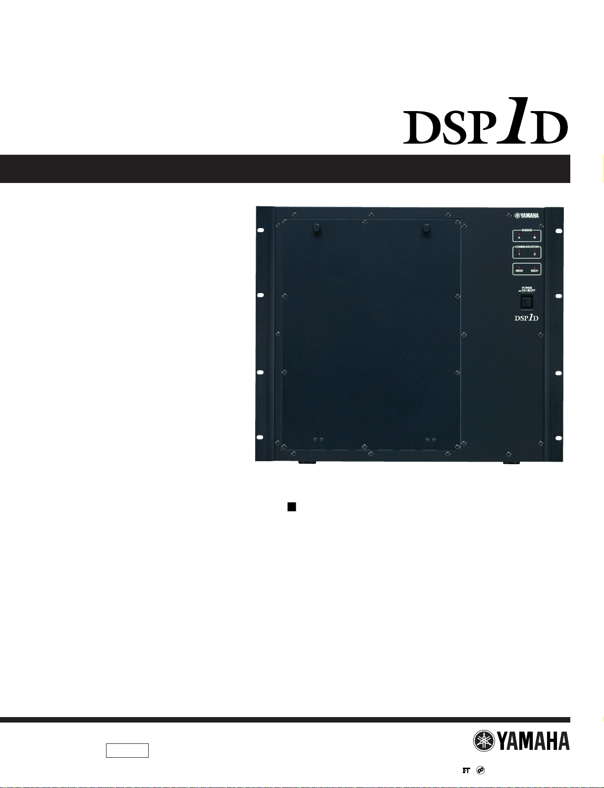
POWER
ON/ OFF
A B
ENGINE ID
1 2
CONTROL I/O
48CH 96CH
INPUT
CONFIGURATION
POWER
ON/ OFF
A B
ENGINE ID
1 2
CONTROL I/O
48CH 96CH
INPUT
CONFIGURATION
22
22
IN
OUT
IN
2
OUT
IN
1
1IN531 97531
2 OUT 6 4 2 10 8 6 4 2
OUT
THRU
PC
CONTROL
WORD CLOCK
TIME CODE IN
GPI
RS-422
REMOTE
IN
OUT
OFF
ON
RS-232-C
USB
75
MIDI
OUTPUT INPUT
CONTROL I/O
CONSOLE
CONSOLE
I/O
CASCADE
DIGITAL I/O
1 IN531 975 31
2 OUT 6 4 2 10 8 6 4 2
OUTPUT INPUT
CONSOLE
I/O
CASCADE
DIGITAL I/O
22
22
IN
OUT
IN
2
OUT
IN
1
OUT
THRU
PC
CONTROL
WORD CLOCK
TIME CODE IN
GPI
RS-422
REMOTE
IN
OUT
OFF
ON
RS-232-C
USB
75
MIDI CONTROL I/O
CONSOLE
1
2
3
4
5
6
7
8
9
10
11
16
12 13 14 15
1
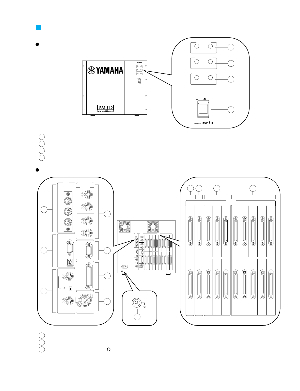
ENGINE ID A/B indicators
2
CONTROL I/O 1/2 indicators
3
INPUT CONFIGURATION 48CH/96CH indicators
4
POWER ON/OFF switch
5
MIDI IN/OUT/THRU connectors
6
PC CONTROL RS-232-C/USB ports
7
WORD CLOCK IN jack, 75 ON/OFF
switch, and WORD CLOCK OUT jack
PANEL LAYOUT
Front Panel
Rear Panel
DSP1D
3-2
Page 6

8
CONSOLE 1, 2 IN/OUT jacks
9
REMOTE RS-422 connector
10
GPI connector
11
TIME CODE IN connector
12
CONSOLE I/O 1, 2 slots
13
CASCADE IN, OUT slots
14
OUTPUT 1–6 slot
15
INPUT 1–10 slot
16
Ground connector
DSP1D
3-3
Page 7
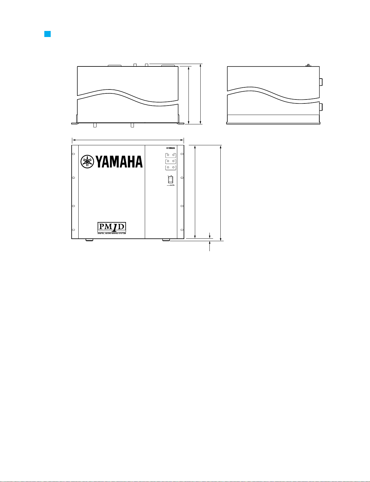
DIMENSIONS
POWER
ON/ OFF
A B
ENGINE ID
1 2
CONTROL I/O
48CH 96CH
INPUT
CONFIGURATION
460.8
450
480
399.2
408.7
9.5
DSP1D
Unit: mm
3-4
Page 8
[1][2][3][5][6][7] [4][8][9][10][1][2][3][4][5][6][IN][OUT][1][2]
[INPUT][OUTPUT][CASCADE]
[CONSOLE I/O]
[CONTROL I/O]
[CONSOLE]
[1]
[2]
[REMOTE]
[GPI]
[TIME CODE IN]
[DIGITAL I/O]
[POWER]
[ON/OFF]
FOR DSP1D-EX
[IN]
[OUT]
[IN]
[OUT]
[RS-422]
[MIDI]
[PC CONTROL]
[WORD CLOCK]
[IN]
[OUT]
[THRU]
[RS-232-C]
[USB]
[IN][
75
]
[OUT]
[ON]
[OFF]
[CONTROL I/O]
[ENGINE ID]
[INPUT CONFIGURATION]
[A] [B]
[1] [2]
[48CH] [96CH]
POWER UNIT
FAN
8P
CN200
3P
CN1
CN809
3P
CN300
2P
CN8
10P
CN101
50P
CN802
50P
CN801
4P
CN604
4P
CN504
4P
CN404
4P
CN304
4P
CN204
4P
CN104
CIB
EMB
EDB
IDB
IDB
GDB
PDB
JK1
JK1
JK1
JK1
JK1
JK2
JK2
JK2
JK3
JK4
JK5
JK6
LED2
PSB2
MB11
IFC1
**
************
**
6P
CN9
8P
CN7
8P
CN6
8P
CN5
8P
CN4
9P
CN3
4P
CN10
8P
CN803
CN103
96P
CN703
CN102
96P
CN702
CN101
96P
CN701
CN103
96P
CN603
CN102
96P
CN602
CN101
96P
CN601
CN652
96P
CN503
CN651
96P
CN502
CN650
96P
CN501
CN3
96P
CN403
CN2
96P
CN402
CN1
96P
CN401
CN3
96P
CN303
CN2
96P
CN302
CN1
96P
CN301
CN904
96P
CN203
CN903
96P
CN202
CN902
96P
CN201
CN902
96P
CN103
CN901
96P
CN102
CN101
96P
CN102
CN102
96P
CN102
CN103
96P
CN102
CN104
96P
CN102
CN201
96P
CN102
CN202
96P
CN102
CN203
96P
CN102
CN301
96P
CN102
CN302
96P
CN102
CN303
96P
CN100
CN811
3P
CN810
96P
CN100
CN900
96P
CN101
CN100
96P
CN102
2P
FG
50P
CN901
50P
CN900
50P
CN950
14P
CN808
30P
CN801
30P
CN802
50P
CN807
50P
CN806
4P
CN105
4P
CN305
4P
CN505
4P
CN605
50P
CN804
50P
CN803
3P
CN405
50P
CN805
50P
CN952
50P
CN955
50P
CN954
50P
CN956
30P
CN951
30P
CN953
14P
CN957
KEC-92539-2
1
DSP1D
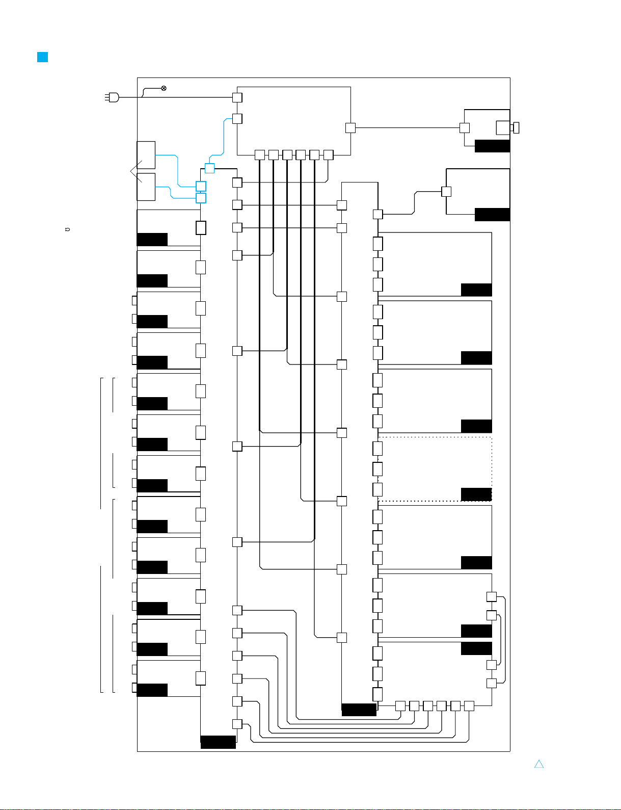
CONNECTOR CIRCUIT DIAGRAM
4
Page 9
Circuit Board CN No. Pin No.
POWER UNIT
CN3
2
3
4
6
7
8
9
1 MB11 1
2
1
2
4
5
4
5
CN204
CN404
CN204
CN404
Circuit Board CN No. Pin No.
POWER UNIT
CN10 1
4
PSB2 CN200 1
3
POWER UNIT
CN4 1
3
2
4
5
6
7
8
MB11 CN604
IFC1 CN605
MB11 CN604
IFC1 CN605
1
2
1
2
3
4
3
4
POWER UNIT
CN5 1
3
2
4
5
6
7
8
MB11 CN504
IFC1 CN505
MB11 CN504
IFC1 CN505
1
2
1
2
3
4
3
4
POWER UNIT
CN6 1
3
2
4
5
6
7
8
MB11 CN304
IFC1 CN305
MB11 CN304
IFC1 CN305
1
2
1
2
3
4
3
4
POWER UNIT
CN7 1
3
2
4
5
6
7
8
MB11 CN104
IFC1 CN105
MB11 CN104
IFC1 CN105
1
2
1
2
3
4
3
4
LED2 CN101 1
3
2
4
5
6
7
8
MB11 CN803 1
2
3
4
5
6
7
8
POWER UNIT
CN9 1
6
5
IFC1 CN405 1
2
3
KEC-92539-3
DSP1D
5
Page 10
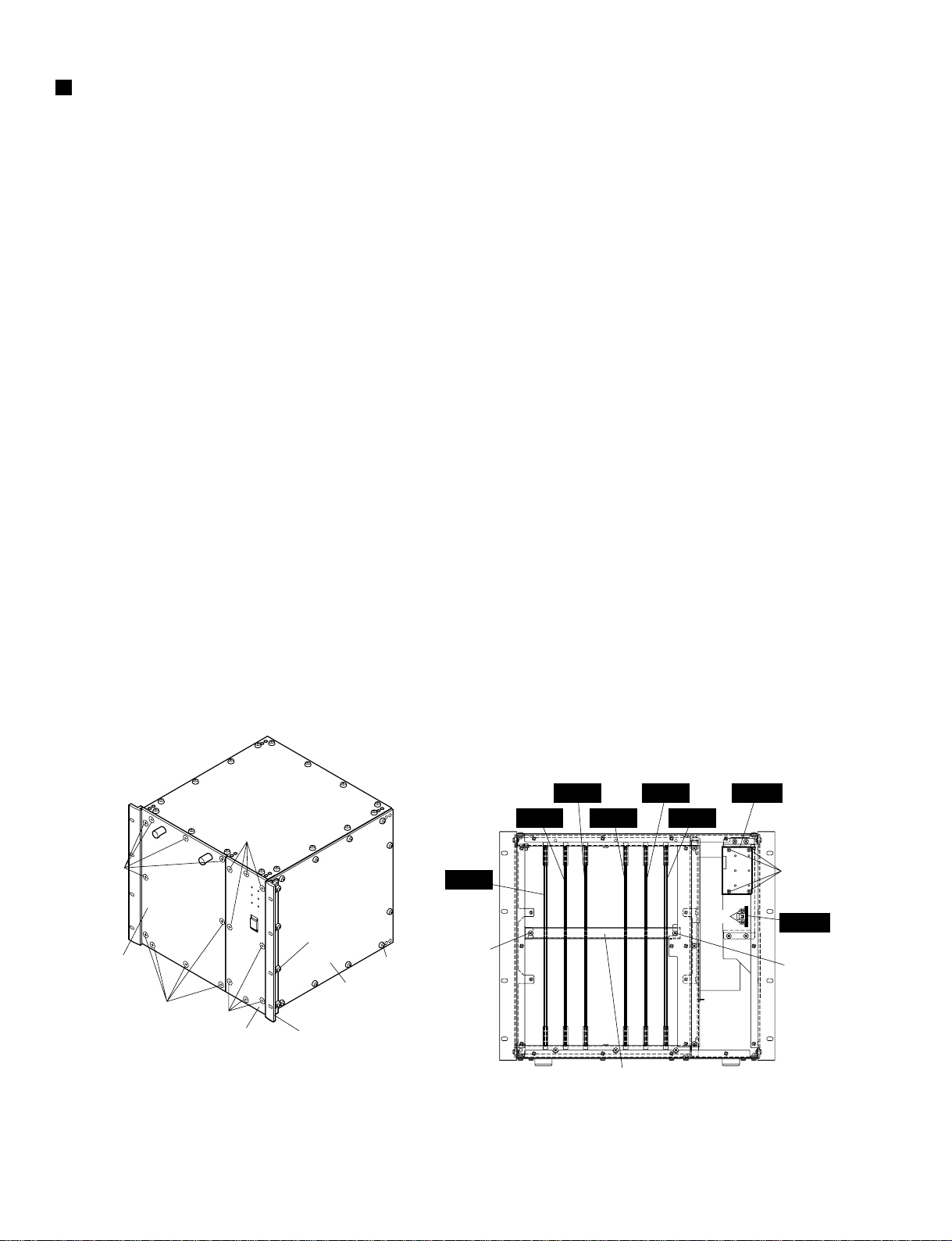
Fig. 1 Fig. 2
[750]
[750]
[960]B x 8
[940] x 10
[905]
[905]
Front cover
Front panel
Side panel-R
Reinforcement angle-A
Right frame
[750]: Oval Head Screw 3.0x6 MFZN2BL (VS153600)
[905]: Oval Head Screw 3.0x6 MFZN2BL (VS153600)
[940]: Bind Head Tapping Screw-B A4.0x8 MFZN2BL (VC688800)
[960B]: Oval Head Screw 3.0x6 MFZN2BL (VS153600)
[325]: Bind Head Tapping Screw-B 3.0x6 MFZN2BL (EP600230)
[330]: Bind Head Screw 3.0x8 MFZN2BL (VB659000)
[850]: Bind Head Screw A4.0x8 MFZN2BL (VP156800)
<Front View>
PDB
GDB
IDB
EDB
EMB
CIB
LED2
PSB2
[325]
[850]
[850]
[330]
DSP1D
6
DISASSEMBLY PROCEDURE
1. GDB, IDB, EDB, EMB and CIB Circuit Boards
1-1 Remove the ten (10) screws marked [905]. The front
cover can then be removed. (Fig. 1)
1-2 Remove the two (2) screws marked [850]. The
reinforcement angle-A can then be removed. (Fig. 2)
1-3 Remove the GDB, IDB, EDB, EMB and CIB circuit
boards by sliding forward. (Fig. 2)
2. PDB Circuit Board
2-1 Remove the front cover. (See procedure 1-1.)
2-2 Remove the reinforcement angle. (See procedure 1-2.)
2-3 Remove the eight (8) screws marked [960A]. The left
frame can then be removed. (Fig. 3)
2-4 Remove the twelve (12) screws marked [920]. The side
panel-L can then be removed. (Fig. 3)
2-5 Remove the PDB circuit board by sliding forward. (Fig. 2)
3. LED2 and PSB2 Circuit Boards
3-1 Remove the eight (8) screws marked [960B]. The right
frame can then be removed. (Fig. 1)
3-2 Remove the eight (8) screws marked [750]. The front
panel can then be removed. (Fig. 1)
3-3 Remove the four (4) screws marked [325]. The LED2
circuit board can then be removed. (Fig. 2)
3-4 Remove the two (2) screws marked [330]. The PSB2
circuit board can then be removed. (Fig. 2)
Page 11
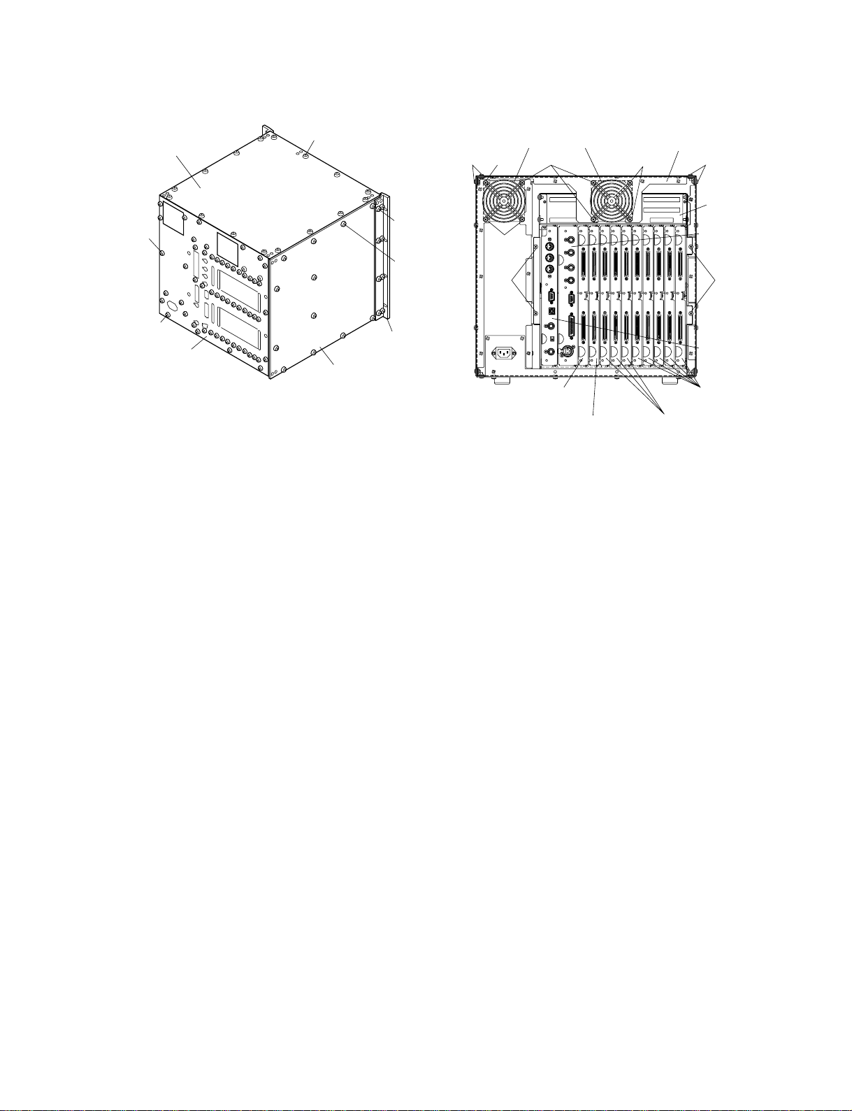
Fig. 3 Fig. 4
[870]: Bind Head Tapping Screw-B A4.0x8 MFZN2BL (VC688800)
[920]: Bind Head Tapping Screw-B A4.0x8 MFZN2BL (VC688800)
[960A]: Oval Head Screw 3.0x6 MFZN2BL (VS153600)
[980]: Bind Head Tapping Screw-B A4.0x8 MFZN2BL (VC688800)
[985]: Bind Head Screw A4.0x8 MFZN2BL (VP156800)
[480]: Bind Head Tapping Screw-B A4.0x8 MFZN2BL (VC688800)
[540]: Bind Head Tapping Screw-B A4.0x8 MFZN2BL (VC688800)
[590]: Bind Head Screw 4.0x35 MFZN2BL (VG605800)
Top cover
Rear panel
[870] x 16
[960A] x 8
[920] x 12
[540] [590]
[590]
[480]
[980] x 58
[985]
Side panel-L
Fan motor RR-TOP frame
JK box assembly
JK1 C.B. assembly
JK5 C.B. assembly
Left frame
<Rear View>
[540][590] [590]
[480]
JK4 C.B. assembly
JK2 C.B. assemblyJK3 C.B. assembly
JK6 C.B. assembly
4. Fan Motor
4-1 Remove the six-teen (16) screws marked [870]. The top
cover can then be removed. (Fig. 3)
4-2 Remove the four (4) screws each marked [590]. The fan
motor A or B can then be removed. (Fig. 4)
5. Power Supply Unit
5-1 Remove the top cover. (See procedure 4-1.)
5-2 Remove the right frame. (See procedure 3-1.)
5-3 Remove the ten (10) screws marked [940]. The side panel-
R can then be removed. (Fig. 1)
5-4 Remove the fifty-eight (58) screws marked [980] and the screw
marked [985]. The rear panel can then be removed. (Fig. 3)
5-5 Remove the eight (8) screws marked [540]. The RR-TOP
frame can then be removed. (Fig. 4)
5-6 Remove the fan motor B. (See procedure 4.)
5-7 Remove the three (3) screws marked [560]. The power
supply unit can then be removed by lifting up. (Fig. 5)
6. JK1-JK6 Circuit Board Assemblies
6-1 Remove the rear panel. (See procedure 5-4.)
6-2 Remove the JK1-JK6 circuit board assemblies by sliding
forward. (Fig. 4)
DSP1D
7
Page 12
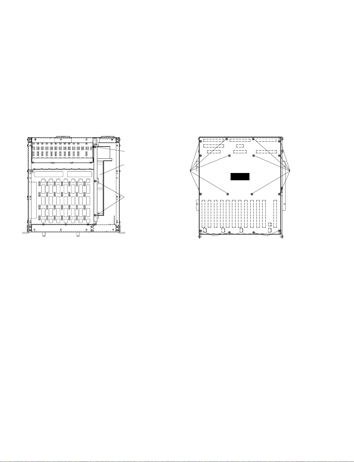
Fig. 5 Fig. 6
[560]: Bind Head Tapping Screw-B A4.0x12 MFZN2BL (VD831800) [110]: Bind Head Tapping Screw-B 3.0x6 MFZN2BL (EP600230)
<Top View> • JK Box Assembly
[560]
[110]
[110]
[560]
Power supply unit
[110]
[110]
IFC1
DSP1D
8
7. IFC Circuit Board
7-1 Remove the top cover. (See procedure 4-1.)
7-2 Remove the left frame and the side panel-L. (See procedure
2-2, 2-3.)
7-3 Remove the rear panel. (See procedure 5-4.)
7-4 Remove the RR-TOP frame. (See procedure 5-5.)
7-5 Remove the four (4) screws marked [480]. The JK box
assembly can then be removed. (Fig. 4)
7-6 Remove the six-teen (16) screws marked [110]. The IFC1
circuit board can then be removed. (Fig. 6)
8. MB11 Circuit Board
8-1 Remove the top cover. (See procedure 4-1.)
8-2 Remove the left frame and the side panel-L. (See procedure
2-2, 2-3.)
8-3 Remove the rear panel. (See procedure 5-4.)
8-4 Remove the RR-TOP frame. (See procedure 5-5.)
8-5 Remove the JK box assembly. (See procedure 7-5.)
8-6 Remove the eight-teen (18) screws marked [430] and the
two (2) screws marked [450]. The MB11 circuit board can
then be removed with the reinforcement angle-B. (Fig. 7)
8-7 Remove the six (6) screws marked [420]. The
reinforcement angle-B can then be removed from the
MB11 circuit board. (Fig. 8)
Page 13
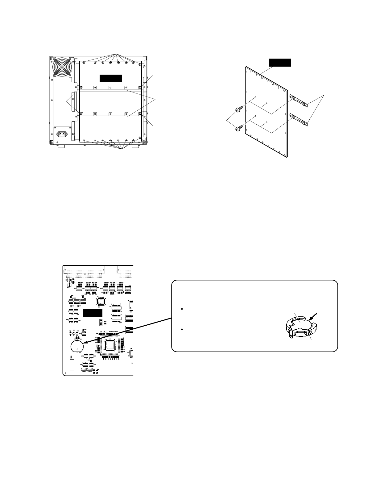
Fig. 7 Fig. 8
[430]: Bind Head Tapping Screw-B 3.0x6 MFZN2BL (EP600230)
[450]: Bind Head Tapping Screw-B 3.0x6 MFZN2BL (EP600230) [420]: Bind Head Tapping Screw-B 3.0x6 MFZN2BL (EP600230)
<Rear View>
[450]
[430]
[430]
Reinforcement
angle-B
Reinforcement angle-B
[450]
[430]
[420]
MB11
MB11
Fig. 9
Battery VN103500
VN103600(Battery holder for VN103500)
Notice for back-up battery removal
Push the battery as shown in figure,
then the battery will pop up.
Druk de batterij naar beneden zoals
aangeven in de tekening, de batterij
springt dan naar voren.
Battery
Battery holder
EMB
DSP1D
9
9. Replacement of the Lithium Battery
9-1 Remove the EMB circuit board. (See procedure 1.)
9-2 The lithium battery can be replacement on the EMB
circuit board. (Fig. 9)
* The lithium battery is not a part of the EMB circuit board.
When you replace the EMB circuit board, remove the
lithium battery and install it in the new circuit board.
Page 14
PIN
NO.
I/O FUNCTIONNAME
PIN
NO.
I/O FUNCTIONNAME
1
2
3
4
5
6
7
8
9
10
11
12
13
14
15
16
17
18
19
20
21
22
23
24
25
26
27
28
29
30
31
32
33
34
35
36
37
38
39
40
41
42
43
44
45
46
47
48
49
50
51
52
53
54
55
56
PE14
PE15
VSS
A0
A1
A2
A3
A4
A5
A6
A7
A8
A9
A10
A11
A12
A13
A14
A15
A16
VCC
A17
VSS
/RAS
/CASL
/CASH
VSS
RDWR / PB5
A18
A19
A20
PB9 /A21
VSS
/RD
/WDTOVF
/WRH
VCC
/WRL
VSS
/CS1
/CS0
PA9 / TCLKD
/IRQ2 / TCLKC
/CS3
/CS2
/IRQ1
TXD
RXD
/IRQ0
PA1 / TXD0
PA0 / RXD0
D15
D14
D13
VSS
D12
O
O
I
O
O
O
O
O
O
O
O
O
O
O
O
O
O
O
O
O
I
O
I
O
O
O
O
O
O
O
O
O
I
O
O
O
I
O
I
O
O
O
I
O
O
I
O
I
I
O
I
I/O
I/O
I/O
I
I/O
Port E
Port E
Ground
Address bus
Power supply
Address bus
Ground
Row address strobe
Column address strobe (low)
Column address strobe (high)
Ground
DRAM read/write / Port B
Address bus
Port B / Address bus
Ground
Read
Watch dog timer overflow
High write
Power supply
Low write
Ground
Chip select
Chip select
Port A / Timer clock
Interrupt request / Timer clock
Chip select
Chip select
Interrupt request
Data transmission
Data reception
Interrupt request
Port A / Data transmission
Port A / Data reception
Data bus
Ground
Data bus
57
58
59
60
61
62
63
64
65
66
67
68
69
70
71
72
73
74
75
76
77
78
79
80
81
82
83
84
85
86
87
88
89
90
91
92
93
94
95
96
97
98
99
100
101
102
103
104
105
106
107
108
109
110
111
112
D11
D10
D9
D8
VSS
D7
D6
D5
VCC
D4
D3
D2
D1
D0
VSS
XTAL
MD3
EXTAL
MD2
NMI
VCC
MD1
MD0
PLLVCC
PLLCAP
PLLVSS
PA15 / CK
/RES
PE0
PE1
PE2
PE3
PE4
VSS
AN0 / PF0
AN1 / PF1
AN2 / PF2
AN3 / PF3
AN4 / PF4
AN5 / PF5
AVSS
AN6 / PF6
AN7 / PF7
AVCC
VSS
PE5
VCC
PE6
PE7
PE8
PE9
PE10
VSS
PE11
PE12
PE13
I/O
I/O
I/O
I/O
I
I/O
I/O
I/O
I
I/O
I/O
I/O
I/O
I/O
I
I
I
I
I
I
I
I
I
I
I
I
O
I
I
I
I
I
I
I
I
I
I
I
I
I
I
I
I
I
I
O
I
O
O
O
O
O
I
O
O
O
Data bus
Ground
Data bus
Power supply
Data bus
Ground
Crystal oscillator
Mode control
Crystal oscillator
Mode control
Non-maskable interrupt request
Power supply
Mode control
Mode control
PLL Power supply
PLL capacitor
PLL Ground
Port A / Clock
Reset
Port E
Ground
Analog input / Port F
Analog ground
Analog input / Port F
Analog input / Port F
Power supply
Ground
Port E
Power supply
Port E
Ground
Port E
HD6477042AF28 (XY715A00) CPU
IC127
IC101
EMB:
PDB:
CIB:
GDB:
IC129,139
IC100
IC100
IC100
EDB:
IDB:
DSP1D
10
LSI PIN DESCRIPTION
HD6477042AF28 (XY715A00) CPU ···················································································· 10
HD6477043AF33 (XY716A00) CPU ···················································································· 11
YSS910-S (XV988A00) DSP6 (Digital Signal Processor)···················································· 12
YSS904-F (XV989A00) DSP5 (Digital Signal Processor) ···················································· 13
SGH609080F-47F (XU235A00) ATSC ················································································ 14
YM3436DK (XG948E0) DIR2 (Digital Format Interface Receiver)······································· 15
AM7992BPC (XW277A00) SIA (Serial Interface Adapter) ·················································· 15
ICS2008A (XV619A00) T.C. Reader/Generator································································· 16
PDIUSBD12PW (XW583A00) USB Interface ····································································· 16
Page 15
DSP1D
11
PIN
NO.
I/O FUNCTIONNAME
PIN
NO.
I/O FUNCTIONNAME
1
2
3
4
5
6
7
8
9
10
11
12
13
14
15
16
17
18
19
20
21
22
23
24
25
26
27
28
29
30
31
32
33
34
35
36
37
38
39
40
41
42
43
44
45
46
47
48
49
50
51
52
53
54
55
56
57
58
59
60
61
62
63
64
65
66
67
68
69
70
71
72
/WRHH
/DACK0/PE14
/WRHL
CASHH/PA21
DACK1/PE15
VSS
A0
A1
A2
A3
A4
VCC
A5
VSS
A6
A7
A8
A9
A10
A11
A12
A13
A14
A15
A16
VCC
A17
VSS
/CASHL/PA20
PA19
/RAS/PB2
/CASL/PB3
PA18
/CASH/PB4
VSS
RDWR/PB5
A18
A19
A20
VCC
A21
VSS
/RD
/WDTOVF
D31
D30
/WRH
/WRL
/CS1
/CS0
/IRQ3/PA9
/IRQ2/PA8
/CS3
/CS2
VSS
D29
D28
D27
D26
D25
VSS
D24
VCC
D23
D22
D21
D20
D19
D18
D17
VSS
D16
O
O
O
I/O
O
I
O
O
O
O
O
I
O
I
O
O
O
O
O
O
O
O
O
O
O
I
O
I
I/O
I/O
O
O
I/O
O
I
O
O
O
O
I
O
I
O
O
I/O
I/O
O
O
O
O
I/O
I/O
O
O
I
I/O
I/O
I/O
I/O
I/O
I
I/O
I
I/O
I/O
I/O
I/O
I/O
I/O
I/O
I
I/O
HH write
DAM transfer strobe/Port E
HL write
HH Column address strobe/Port A
DMA transfer strobe/Port E
Ground
Address bus
Power supply
Address bus
Ground
Address bus
Power supply
Address bus
Ground
HL Column address strobe/Port A
Port A
Row address strobe/Port B
Column address strobe (low) /Port B
Port A
Column address strobe (high) /Port B
Ground
DRAM read/write /Port B
Address bus
Power supply
Address bus
Ground
Read
Watch dog timer overflow
Data bus
Data bus
High write
Low write
Chip select
Chip select
Interrupt request/Port A
Interrupt request/Port A
Chip select
Chip select
Ground
Data bus
Ground
Data bus
Power supply
Data bus
Ground
Data bus
73
74
75
76
77
78
79
80
81
82
83
84
85
86
87
88
89
90
91
92
93
94
95
96
97
98
99
100
101
102
103
104
105
106
107
108
109
110
111
112
113
114
115
116
117
118
119
120
121
122
123
124
125
126
127
128
129
130
131
132
133
134
135
136
137
138
139
140
141
142
143
144
D15
D14
D13
D12
VCC
D11
VSS
D10
D9
D8
D7
D6
VCC
D5
VSS
D4
D3
D2
D1
D0
VSS
XTAL
MD3
EXTAL
MD2
NMI
VCC
PA16
PA17
MD1
MD0
PLLVCC
PLLCAP
PLLVSS
CK/PA15
/RES
/DREQ0/TIOC0A/PE0
PE1
/DREQ1/PE2
VCC
PE3
PE4
PE5
PE6
VSS
AN0 /PF0
AN1/ PF1
AN2 /PF2
AN3 /PF3
AN4 /PF4
AN5/PF5
AVSS
AN6/PF6
AN7/PF7
AVREF
AVCC
VSS
RxDO
TxDO
/IRQ0/SCK0
RxD1
TxD1
VCC
/IRQ1/SCK1
PE7
PE8
PE9
PE10
VSS
TIOC3D/PE11
PE12
PE13
I/O
I/O
I/O
I/O
I
I/O
I
I/O
I/O
I/O
I/O
I/O
I
I/O
I
I/O
I/O
I/O
I/O
I/O
I
I
I
I
I
-
I
I/O
I/O
I
I
I
I
I
I/O
I
I/O
I/O
I/O
I
I/O
I/O
I/O
I/O
I
I
I
I
I
I
I
I
I
I
I
I
I
I
O
I
I
I/O
I
I
I/O
I/O
I/O
I/O
I
I/O
I/O
I/O
Data bus
Power supply
Data bus
Ground
Data bus
Power supply
Data bus
Ground
Data bus
Ground
Crystal oscillator
Mode select
Crystal oscillator
Mode select
Non-maskable interrupt
Power supply
Port A
Port A
Mode select
Mode select
PLL Power supply
PLL capacitor
PLL Ground
Clock/Port A
Reset
DMA transfer request/MTU input capture/output compare (ch 0)/Port E
Port E
DMA transfer request/Port E
Power supply
Port E
Ground
Analog input/Port F
Analog ground
Analog input/ Port F
Analog input /Port F
Analog reference voltage
Analog power supply
Ground
Receive data
Transmit data
Interrupt request/Serial clock
Receive data
SCI
Power supply
Interrupt request/Serial clock
Port E
Ground
MTU input capture/output compare (ch 3)/Port E
Port E
Port E
HD6477043AF33 (XY716A00) CPU EMB: IC114
Page 16
PIN
NO.
I/O FUNCTIONNAME
PIN
NO.
I/O FUNCTIONNAME
1
2
3
4
5
6
7
8
9
10
11
12
13
14
15
16
17
18
19
20
21
22
23
24
25
26
27
28
29
30
31
32
33
34
35
36
37
38
39
40
41
42
43
44
45
46
47
48
49
50
51
52
53
54
55
56
57
58
59
60
61
62
63
64
65
66
67
68
69
70
71
72
73
74
75
76
77
78
79
80
81
82
83
84
85
86
87
88
Vdd
Vss
XI
XO
Vdd
/SYNCI
/SYNCO
Vdd
CKI
CKO
CKSEL
Vss
MCKS
/SSYNC
/IC
/TEST
BTYP
/IRQ
TRIG
Vdd
Vss
/CS
/WR
/RD
CA7
CA6
CA5
CA4
CA3
CA2
CA1
Vss
Vdd
CD15
CD14
CD13
CD12
CD11
CD10
CD09
CD08
CD07
CD06
Vss
Vdd
Vdd
CD05
CD04
CD03
CD02
CD01
CD00
/WAIT
Vss
SI0
SI1
SI2
SI3
SI4
SI5
SI6
SI7
Vss
Vdd
SO0
SO1
SO2
SO3
SO4
SO5
SO6
SO7
Vss
DB00
DB01
DB02
DB03
DB04
DB05
DB06
DB07
DB08
DB09
DB10
DB11
DB12
Vdd
Vdd
I
O
I
O
I
O
I
I
I
I
I
I
O
I/O
I
I
I
I/O
I/O
I/O
I/O
I/O
I/O
I/O
I/O
I/O
I/O
I/O
I/O
I/O
I/O
I/O
I/O
I/O
I/O
I/O
I/O
I/O
I/O
I/O
O
I
I
I
I
I
I
I
I
O
O
O
O
O
O
O
O
I/O
I/O
I/O
I/O
I/O
I/O
I/O
I/O
I/O
I/O
I/O
I/O
I/O
Power supply (3.3 V)
Ground
System master clock input (60 MHz or 30 MHz)
System master clock output (High or 30 MHz)
Power supply (5 V)
Sync. signal input
Sync. signal output
Power supply (5 V)
System clock input (30 MHz)
System clock output (30 MHz)
System master clock select (0: 60 MHz, 1: 30 MHz)
Ground
Serial I/O master clock input (128 x Fs)
Serial I/O Sync. signal output
Initial clear
Test mode setting (0: Test, 1: Normal)
Data bus type select (0: 8 bit, 1: 16 bit)
IRQ output
Trigger signal input/output
Power supply (5 V)
Ground
chip select signal input
Write signal input
Read signal input
Address bus of internal register
Ground
Power supply (3.3 V)
Data bus of internal register
Ground
Power supply (3.3 V)
Power supply (5 V)
Data bus of internal register
WAIT output
Ground
Serial data input
Ground
Power supply (5 V)
Serial data output
Ground
Parallel data bus
Power supply (5 V)
Power supply (3.3 V)
89
90
91
92
93
94
95
96
97
98
99
100
101
102
103
104
105
106
107
108
109
110
111
112
113
114
115
116
117
118
119
120
121
122
123
124
125
126
127
128
129
130
131
132
133
134
135
136
137
138
139
140
141
142
143
144
145
146
147
148
149
150
151
152
153
154
155
156
157
158
159
160
161
162
163
164
165
166
167
168
169
170
171
172
173
174
175
176
Vss
DB13
DB14
DB15
DB16
DB17
DB18
DB19
DB20
DB21
DB22
Vss
Vdd
DB23
DB24
DB25
DB26
DB27
DB28
DB29
DB30
DB31
TIMO/DBOB
Vss
Vdd
DA00
DA01
DA02
DA03
DA04
DA05
DA06
DA07
Vss
DA08
DA09
DA10
DA11
DA12
DA13
DA14
DA15
Vss
Vdd
(n.c)
Vdd
DA16
DA17
DA18
DA19
DA20
DA21
DA22
DA23
Vss
DA24
DA25
DA26
DA27
DA28
DA29
DA30
DA31
Vdd
Vss
A00
A01
A02
A03
A04
A05
A06
A07
A08
A09
Vss
Vdd
A10
A11
A12
A13
A14
A15/RAS
A16/CAS
A17/CE
/WE
/OE
Vdd
I/O
I/O
I/O
I/O
I/O
I/O
I/O
I/O
I/O
I/O
I/O
I/O
I/O
I/O
I/O
I/O
I/O
I/O
I/O
I/O
I/O
I/O
I/O
I/O
I/O
I/O
I/O
I/O
I/O
I/O
I/O
I/O
I/O
I/O
I/O
I/O
I/O
I/O
I/O
I/O
I/O
I/O
I/O
I/O
I/O
I/O
I/O
I/O
I/O
I/O
I/O
I/O
O
O
O
O
O
O
O
O
O
O
O
O
O
O
O
O
O
O
O
O
Ground
Parallel data bus
Ground
Power supply (3.3 V)
Parallel data bus
Timing signal output/ Parallel data bus output/ input
Ground
Power supply (5 V)
Memory data bus
Ground
Memory data bus
Ground
Power supply (3.3 V)
Not used
Power supply (5 V)
Memory data bus
Ground
Memory data bus
Power supply (5 V)
Ground
Memory address (SRAM, PSRAM, DRAM)
Ground
Power supply (3.3 V)
Memory address (SRAM, PSRAM, DRAM)
Memory address (SRAM, PSRAM)
Memory address (SRAM, PSRAM), /RAS (DRAM)
Memory address (SRAM, PSRAM), /CAS (DRAM)
Memory address (SRAM), /CE (PSRAM)
Memory write enable signal
Memory output enable signal
Power supply (5 V)
YSS910-S (XV988A00) DSP6 (Digital Signal Processor)
EDB:
GDB:
IDB:
PDB:
IC300,304,350,354,400,404,450,454,500,503,550,553
IC300,305,350,351,400,403,450,451,500,503,550,551,600
IC250,255,300,301,350,351,400,401,450,453,500,501,550,551,600,601
IC500,505,550,551,600,603,650,700,701
DSP1D
12
Page 17
PIN
NO.
I/O
FUNCTION
NAME
PIN
NO.
I/O
FUNCTION
NAME
1
2
3
4
5
6
7
8
9
10
11
12
13
14
15
16
17
18
19
20
21
22
23
24
25
26
27
28
29
30
31
32
33
34
35
36
37
38
39
40
41
42
43
44
45
46
47
48
49
50
51
52
53
54
55
56
57
58
59
60
61
62
63
64
65
66
67
68
69
70
71
72
73
74
75
76
77
78
79
80
81
82
83
84
85
86
87
88
89
90
91
92
93
94
95
96
97
98
99
100
101
102
103
104
NC
NC
NC
NC
Vdd
Vss
XI
XO
Vdd
/SYNCI
/SYNCO
Vdd
CKI
CKO
CKSEL
Vss
MCKD
/SSYNC
/IC
/TEST
NC
NC
NC
Vdd
Vss
/CS
/WR
/RD
CA7
CA6
CA5
CA4
CA3
CA2
CA1
Vss
Vdd
CD15
CD14
CD13
CD12
CD11
CD10
CD09
CD08
CD07
CD06
Vss
NC
NC
NC
NC
NC
NC
NC
NC
Vdd
Vdd
CD05
CD04
CD03
CD02
CD01
CD00
/WAIT
Vss
SIO00
SIO01
SIO02
SIO03
SIO04
SIO05
SIO06
SIO07
Vss
Vdd
SIO08
SIO09
SIO10
SIO11
SIO12
SIO13
SIO14
SIO15
Vss
Vdd
SIO16
SIO17
SIO18
SIO19
SIO20
SIO21
SIO22
SIO23
Vss
Vdd
SIO24
SIO25
SIO26
SIO27
NC
NC
NC
NC
I
O
O
I
O
I
O
I
I
I
I
I
I
I
I
I
I
I
I
I
I
I
I/O
I/O
I/O
I/O
I/O
I/O
I/O
I/O
I/O
I/O
I/O
I/O
I/O
I/O
I/O
I/O
O
I/O
I/O
I/O
I/O
I/O
I/O
I/O
I/O
I/O
I/O
I/O
I/O
I/O
I/O
I/O
I/O
I/O
I/O
I/O
I/O
I/O
I/O
I/O
I/O
I/O
I/O
I/O
I/O
Not used
Ground
Power supply
System master clock input (60 MHz or 30 MHz)
System master clock output (High or 30 MHz)
Ground
Sync. signal input
Sync. signal output
Ground
System clock input (30 MHz)
System clock output (30 MHz)
System master clock select
Power supply
Serial clock input (256 fs)
Serial. signal input
Initial clear
Test mode setting (0: TEST, 1: Normal)
Not used
Ground
Power supply
Chip select
Write enable input
Read enable input
CPU address bus
Power supply
Ground
CPU data bus
Power supply
Not used
Ground
CPU data bus
Wait output
Power supply
Serial data bus
Power supply
Ground
Serial data bus
Power supply
Ground
Serial data bus
Power supply
Ground
Serial data bus
Not used
105
106
107
108
109
110
111
112
113
114
115
116
117
118
119
120
121
122
123
124
125
126
127
128
129
130
131
132
133
134
135
136
137
138
139
140
141
142
143
144
145
146
147
148
149
150
151
152
153
154
155
156
157
158
159
160
161
162
163
164
165
166
167
168
169
170
171
172
173
174
175
176
177
178
179
180
181
182
183
184
185
186
187
188
189
190
191
192
193
194
195
196
197
198
199
200
201
202
203
204
205
206
207
208
NC
NC
NC
NC
SIO28
SIO29
SIO30
SIO31
Vss
Vdd
SIO32
SIO33
SIO34
SIO35
SIO36
SIO37
SIO38
SIO39
Vss
Vdd
SIO40
SIO41
SIO42
SIO43
SIO44
SIO45
SIO46
SIO47
Vss
SIO48
SIO49
SIO50
SIO51
SIO52
SIO53
SIO54
SIO55
Vss
Vdd
Vdd
SIO56
SIO57
SIO58
SIO59
SIO60
SIO61
SIO62
SIO63
NC
NC
NC
NC
NC
NC
NC
NC
Vss
/POE
Vss
PIO00
PIO01
PIO02
PIO03
PIO04
PIO05
PIO06
PIO07
Vss
Vdd
Vdd
PIO08
PIO09
PIO10
PIO11
PIO12
PIO13
PIO14
PIO15
Vss
NC
PIO16
PIO17
PIO18
PIO19
PIO20
PIO21
PIO22
PIO23
Vss
Vdd
Vdd
PIO24
PIO25
PIO26
PIO27
PIO28
PIO29
PIO30
PIO31
Vss
NC
NC
NC
NC
I/O
I/O
I/O
I/O
I/O
I/O
I/O
I/O
I/O
I/O
I/O
I/O
I/O
I/O
I/O
I/O
I/O
I/O
I/O
I/O
I/O
I/O
I/O
I/O
I/O
I/O
I/O
I/O
I/O
I/O
I/O
I/O
I/O
I/O
I/O
I/O
I
I/O
I/O
I/O
I/O
I/O
I/O
I/O
I/O
I/O
I/O
I/O
I/O
I/O
I/O
I/O
I/O
I/O
I/O
I/O
I/O
I/O
I/O
I/O
I/O
I/O
I/O
I/O
I/O
I/O
I/O
I/O
I/O
Not used
Serial data bus
Power supply
Ground
Serial data bus
Power supply
Ground
Serial data bus
Power supply
Serial data bus
Power supply
Ground
Serial data bus
Not used
Power supply
Parallel data bus controll signal
Power supply
Parallel data bus
Power supply
Ground
Parallel data bus
Power supply
Not used
Parallel data bus
Power supply
Ground
Parallel data bus
Power supply
Not used
YSS904-F (XV989A00) DSP5 (Digital Signal Processor)
GDB:
IDB:
PDB:
IC250,251,650,651,750,751,800
IC650,651,700,701,750,751,800,801
IC250,251,300,301,350,351,400,401,450,750,751
DSP1D
13
Page 18
PIN
NO.
I/O FUNCTIONNAME
PIN
NO.
I/O FUNCTIONNAME
1
2
3
4
5
6
7
8
9
10
11
12
13
14
15
16
17
18
19
20
21
22
23
24
25
26
27
28
29
30
31
32
33
34
35
36
37
38
39
40
syncati
mccti
mcbti
VCC
GND
mcati
GND
siat0
siat1
siat2
siat3
ati
GND
ato
soat3
soat2
soat1
soat0
VCC
GND
mcato
GND
mcbto
mccto
syncato
clksel
ato-sel0
ato-sel1
bitsel2
bitsel1
bitsel0
VCC
GND
ext-sync2
ui0
ui1
ui2
ui3
si-sel0
si-sel1
I
I
I
I
I
I
I
I
I
O
O
O
O
O
I
I
I
I
I
I
I
Synch. word input terminal for ati,
siat3-0 input
64 fs clock input terminal for ati,
siat3-0 input
128 fs clock input terminal for ati,
siat3-0 input
Power supply (+5 V)
Ground
256 fs clock input terminal for ati,
siat3-0 input
Ground
Serial data input terminal
Optical input terminal
Ground
Optical output terminal
Serial data output terminal
Power supply (+5 V)
Ground
256 fs clock input terminal for ato,
soat3-0 output
Ground
128 fs clock input terminal for ato,
soat3-0 output
64 fs clock input terminal for ato,
soat3-0 output
Synch. word input terminal for ato,
soat3-0 output
Clock select terminal for ato,
soat 3-0 output
0: mcato,mcbto,mccto,syncato
1: mcai,mcbi,mcci,synci
Format select terminal for ato,
soat3-0 output
Format select terminal for ato,
soat3-0 output
Bit shift select terminal for the ato output
Power supply (+5 V)
Ground
Synch. detect output terminal 2
U-bit input terminal for optical output
input format select terminal for si3-0
input format select terminal for si3-0i
41
42
43
44
45
46
47
48
49
50
51
52
53
54
55
56
57
58
59
60
61
62
63
64
65
66
67
68
69
70
71
72
73
74
75
76
77
78
79
80
synci
mcci
mcbi
VCC
GND
mcai
GND
si0
si1
si2
si3
GND
so3
so2
so1
so0
VCC
GND
mcao
GND
mcbo
mcco
synco
so-sel1
so-sel0
uo3
uo2
uo1
uo0
ext-sync1
VCC
GND
clk
GND
/res
GND
wc-at
mute
ati-sel1
ati-sel0
I
I
I
I
I
I
I
I
O
O
O
O
I
I
I
I
I
I
O
O
O
O
O
I
I
O
I
I
I
Synch. word input terminal for si3-0 input
64 fs clock input terminal for si3-0 input
128 fs clock input terminal for si3-0 input
Power supply (+5 V)
Ground
256 fs clock input terminal for si3-0 input
Ground
Serial data input terminal
Ground
Serial data output terminal
Power supply (+5 V)
Ground
256 fs clock input terminal for so3-0 output
Ground
128 fs clock input terminal for so3-0 output
64 fs clock input terminal for so3-0 output
Synch. word input terminal for so3-0 output
Format select terminal for soat3-0 output
Format select terminal for soat3-0 output
U-bit output terminal for optical output
Synch. detect output terminal 1
Power supply (+5 V)
Ground
Clock input terminal for word clock extract
Ground
System reset input terminal
Ground
Word clock output terminal
Data mute input terminal
Input format select terminal for ati, siat3-0.
input format select terminal for ati, siat3-0.
SGH609080F-47F (XU235A00) ATSC
1
1
0
0
so sel1
1
0
1
0
so sel0
not enable to set
so0
so2, 0
so3-0
(8ch/line)
(4ch/line)
(2ch/line)
input format
1
1
0
0
ati sel1
1
0
1
0
ati sel0
ati
ati0
ati2, 0
ati3-0
(8ch/line)
(4ch/line)
(2ch/line)
input format
1
1
0
0
ato sel1
0: mcato,mcbto,mccto,syncato
1: mcai,mcbi,mcci,synci
1
0
1
0
ato sel0
ato
soat0
soat2, 0
soat3-0
(8ch/line)
(4ch/line)
(2ch/line)
output format
1
1
0
0
si sel1
1
0
1
0
si sel0
not enable to set
si0
si2, 0
si3-0
(8ch/line)
(4ch/line)
(2ch/line)
input format
IC100,101,113,114
IC109,110,118,119
JK2:
JK4:
JK1:
JK3:
IC109,110,119,120
IC111-114
DSP1D
14
Page 19
PIN
NO.
I/O FUNCTIONNAME
PIN
NO.
I/O FUNCTIONNAME
1
2
3
4
5
6
7
8
9
10
11
12
CLSN
RX
RENA
RCLK
TSEL
GND1
GND2
X1
X2
TX
TCLK
TENA
O
O
O
O
I/O
-
I
I
I
O
I
Collision (Output, TTL Active HIGH)
Receive Data
Receive Enable (Output, TTL Acvtive HIGH)
Receive Clock
Transmit Mode Select (Output, Open Collector;
Input, Sense Amplifier)
High Current Ground
Logic Ground
Biased Crystal Oscillator
Biased Crystal Oscillator
Transmit
Transmit Clock
Transmit Enable
13
14
15
16
17
18
19
20
21
22
23
24
Collision+
Collision-
Receive+
Receive-
/TEST
Vcc1
Vcc2
PF
RF
GND3
Transmit+
Transmit-
I
I
I
I
I
-
I
O
-
O
O
Collision
Collision
Receiver
Receiver
Test Control
High Current and Logic Supply
Voltage-Controlled Oscillator Supply
Receive Path Vco Phase-Locked Loop Filter
Frequency Setting Voltage-Controlled
Oscillator (Vco) Loop Filter (Output)
Voltage-Controlled Oscillator Ground
Transmit
Transmit
AM7992BPC (XW277A00) SIA (Serial Interface Adapter)
CIB: IC112-115
DSP1D
15
PIN
NO.
I/O FUNCTIONNAME
PIN
NO.
I/O FUNCTIONNAME
1
2
3
4
5
6
7
8
9
10
11
12
13
14
15
16
17
18
19
20
21
22
DAUX
HDLT
DOUT
VFL
OPT
SYNC
MCC
WC
MCB
MCA
SKSY
XI
XO
P256
LOCK
Vss
TC
DIM1
DIM0
DOM1
DOM0
KM1
I
O
O
O
O
O
O
O
O
O
I
I
O
O
O
O
I
I
I
I
I
Auxiliary input for audio data
Asynchronous buffer operation flag
Audio data output
Parity flag output
Fs x 1 Synchronous output signal for DAC
Fs x 1 Synchronous output signal for DSP
Fs x 64 Bit clock output
Fs x 1 Word clock output
Fs x 128 Bit clock output
Fs x 256 Bit clock output
Clock synchronization control input
Crystal oscillator connection or external
clock input
Crystal oscillator connection
VCO oscillating clock connection
PLL lock flag
Logic section power (GND)
PLL time constant switching output
Data input mode selection
Data input mode selection
Data output mode selection
Data output mode selection
Clock mode switching input 1
23
24
25
26
27
28
29
30
31
32
33
34
35
36
37
38
39
40
41
42
43
44
RSTN
Vdda
CTLN
PCO
(NC)
CTLP
Vssa
TSTN
KM2
KM0
FS1
FS0
CSM
EXTW
DDIN
LR
Vdd
ERR
EMP
CD0
CCK
CLD
I
I
O
I
I
I
I
O
O
I
I
I
O
O
O
O
I
I
System reset input
VCO section power (+5 V)
VCO control input N
PLL phase comparison output
VCO control input P
VCO section power (GND)
Test terminal. Open for normal use
Clock mode switching input 2
Clock mode switching input 0
Channel status sampling frequency
display output 1
Channel status sampling frequency
display output 0
Channel status output method selection
External synchronous auxiliary input
word clock
EIAJ (AES/EBU) data input
PLL word clock output
Logic section power (+5 V)
Data error flag output
Channel status emphasis control code
output
3-wire type microcomputer interface data
output
3-wire type microcomputer interface clock
input
3-wire type microcomputer interface load
input
YM3436DK (XG948E0) DIR2 (Digital Format Interface Receiver)
IC112,121
IC110,126
IC202
JK1:
JK3:
JK6
IFC1:
JK2:
JK4:
IC604-606
IC112,121
IC112,120
Page 20
DSP1D
16
PIN
NO.
I/O FUNCTIONNAME
PIN
NO.
I/O FUNCTIONNAME
1
2
3
4
5
6
7
8
9
10
11
12
13
14
15
16
17
18
19
20
21
22
INTR
RESET
FRAME
CLICK
LTCIN-
LTCIN+
LTCOUT
LFC
XTAL2
XTAL1
AVDD
AVSS
COUT
YOUT
C2
Y2
C1
Y1
STHRESH
CTHRESH
DTHRESH
RXD
O
I
I
I
I
I
O
I
O
I
-
O
O
I
I
I
I
I
I
I
I
Interrupt request
Master reset
Color frame A / B input
LTC SYNC input
SMPTE LTC input SMPTE LTC input +
SMPTE LTC output
External RC circuit
14.318 MHz crystal oscillator
14.318 MHz crystal oscillator
Analog power supply
Analog ground
C(Chroma) output
Y(Luma) output
C(Chroma) input
Y(Luma) input
C(Chroma) input
Y(Luma) input
SYNC threshold bypass input
Clamp threshold bypass input
Data threshold bypass input
UART receive data
23
24
25
26
27
28
29
30
31
32
33
34
35
36
37
38
39
40
41
42
43
44
CTS
TXD
RTS
LRCLK
VITCGATE
VITCOUT
A0
A1
/SMPTECS
/UARTSC
/IOR
VSS
VDD
/IOW
D0
D1
D2
D3
D4
D5
D6
D7
I
O
O
O
O
O
I
I
I
I
I
-
I
I/O
I/O
I/O
I/O
I/O
I/O
I/O
I/O
Clear to send
UART transmit data
Ready to send
SMPTE LTC receive clock
VITE cord is for video overlay
SMPTE VITE output
Address bus
Address bus
SMPTE port chip select
UART chip select
Read enable
Digital ground
Digital power supply
Write enable
Data bus
ICS2008A (XV619A00) T.C. Reader/Generator CIB: IC136
PIN
NO.
I/O FUNCTIONNAME
PIN
NO.
I/O FUNCTIONNAME
1
2
3
4
5
6
7
8
9
10
11
12
13
14
DATA0
DATA1
DATA2
DATA3
GND
DATA4
DATA5
DATA6
DATA7
ALE
CS_N
SUSPEND
CLKOUT
INT_N
I/O
I/O
I/O
I/O
I/O
I/O
I/O
I/O
I
I
I/O
O
O
Bit 0 of bi-directional data.
Bit 1 of bi-directional data.
Bit 2 of bi-directional data.
Bit 3 of bi-directional data.
Ground
Bit 4 of bi-directional data.
Bit 5 of bi-directional data.
Bit 6 of bi-directional data.
Bit 7 of bi-directional data.
Address Latch Enable.
Chip Select (Active Low).
Device is in Suspend state.
Programmable Output Clock (slew-rate controlled)
interrupt (Active Low)
15
16
17
18
19
20
21
22
23
24
25
26
27
28
RD_N
WR_N
DMREQ
DMACK_N
EOT_N
RESET_N
GL_N
XTAL1
XTAL2
Vcc
D-
D+
Vout3.3
A0
I
I
O
I
I
I
O
I
O
-
-
-
I
Read Strobe (Active Low)
Write Strobe (Active Low)
DMA Request.
DMA Acknowledge (Active Low).
End of DMA Transfer (Active Low).
Reset (Active Low and asynchronous).
Built-in Power-On-Reset circuit
GoodLink LED indicator (Active Low)
Crystal Connection 1 (6 MHz)
Crystal Connection 2 (6 MHz)
Voltage supply (4.0-5.5 V)
USB D-data line
USB D+data line
3.3 V regulated output.
Address bit. A0=1 selects command
instruction; A0=0 selects the data phase.
PDIUSBD12PW (XW583A00) USB Interface JK6: IC105
Page 21
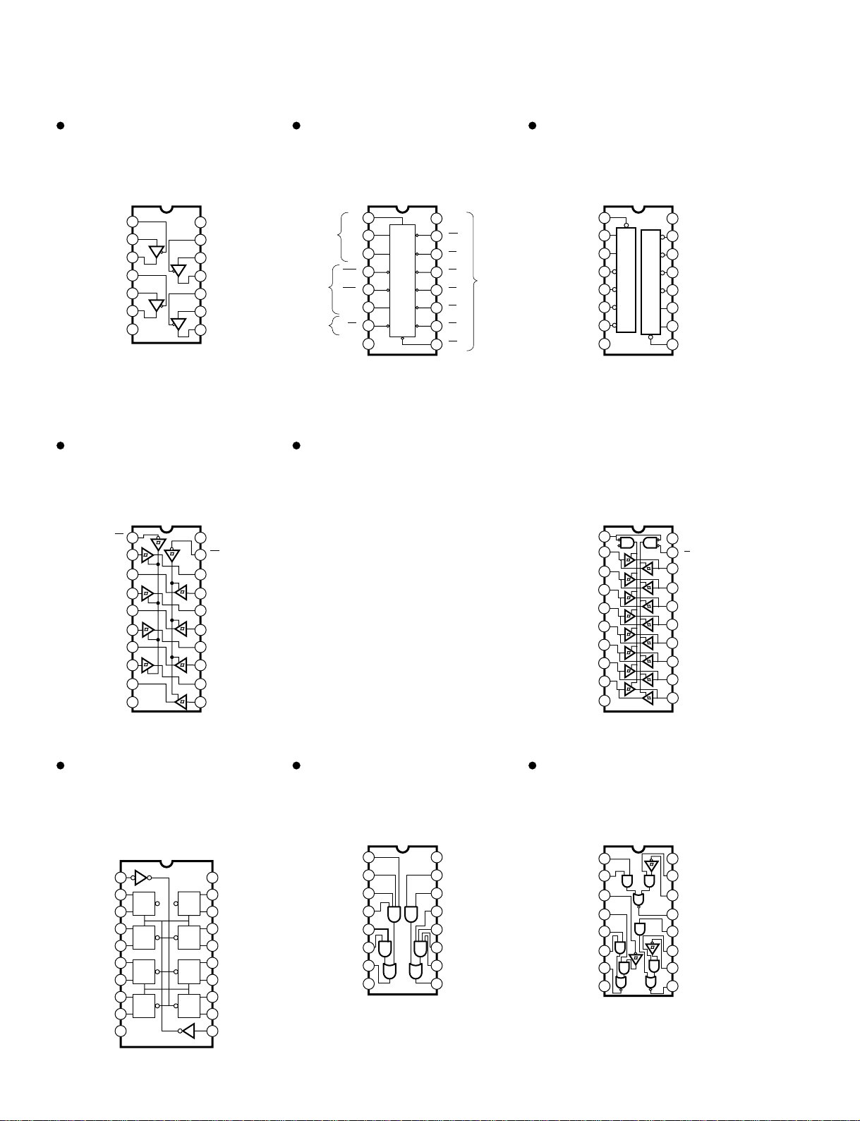
IC BLOCK DIAGRAM
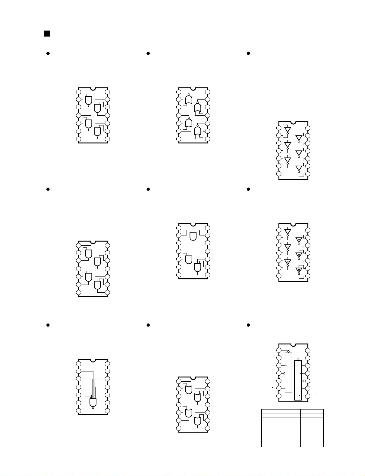
HD74LV00AFPEL (IS000000)
Quad 2 Input NAND
EMB: IC101,105
HD74LV02AFPEL (IS00020)
Quad 2 Input NOR
CIB:
JK3:
HD74LV04AFPEL (IS000400)
HD74LV05AFPEL (IS000500)
SN74LS06NSR (XP985A00)
Hex Inverter
CIB:
EMB:
IDB:
JK1:
JK3:
JK5:
PDB:
HD74LV08AFPEL (IS000800)
Quad 2 Input AND
CIB:
EMB:
IDB:
JK1:
JK4:
HD74LV11AFPEL (IS001100)
Triple 3 Input AND
CIB:
EMB:
HD74LV14AFPEL (IS001400)
Hex Inverter
JK6: IC107
HD74HC30FPTL (XQ970A00)
8 Input NAND
EMB: IC106
HD74LV32AFPEL (IS003200)
Quad 2 Input OR
CIB:
GDB:
IDB:
JK2:
JK4:
HD74LV74AFPEL (IS007400)
Dual D-Type Flip-Flop
CIB: IC111
1
2
3
1A
1Y
42A
52B
62Y
7Vss
1B
14
13
12
VDD
4A
11 4Y
10 3B
9 3A
8 3Y
4B
1
2
3
1Y
1B
42Y
52A
62B
7Vss
1A
14
13
12
VDD
4A
11 4B
10 3Y
9 3A
8 3B
4Y
1
2
3
4
5
6
7
1A
1Y
2A
2Y
3A
3Y
Vss
14
13
12
11
10
9
8
VDD
6A
6Y
5A
5Y
4A
4Y
1
2
3
1A
1Y
42A
52B
62Y
7
VSS
1B
14
13
12
VDD
4A
11 4Y
10 3B
9 3A
8 3Y
4B
1
2
3
1A
2A
42B
52C
62Y
7
VSS
1B
14
13
12
VDD
1Y
11 3C
10 3B
9 3A
8 3Y
1C
1
2
3
4
5
6
7
1A
1Y
2A
2Y
3A
3Y
GND
14
13
12
11
10
9
8
VDD
6A
6Y
5A
5Y
4A
4Y
1
2
3
A
C
4D
5E
6F
7
GND
B
14
13
12
Vcc
H
11 G
10 NC
9 NC
8 Y
NC
1
2
3
1A
1Y
42A
52B
62Y
7GND
1B
14
13
12
Vcc
4A
11 4Y
10 3B
9 3A
8 3Y
4B
INPUTS OUTPUTS
PR CLR CLK D Q Q
L
H
H
L
H
Q
O
H
L
H
H
L
Q O
X
X
X
H
L
X
X
X
X
f
f
L
H
L
L
H
H
H
L
H
L
H
H
H
1
2
3
4
5
6
7
1CLR
1D
1CK
1PR
1Q
1Q
GND
14
13
12
11
10
9
8
VCC
2CLR
CLR
2D
D
2CK
CK
2PRPR
2Q
2Q
Q
Q
CLR
D
CK
PR
Q
Q
IC103,117,128,151
IC107,108,151
IC111,116
IC102,141
IC100,141
IC108
IC109,IC115
EDB:
GDB:
IFC1:
JK2:
JK4:
JK6:
IC109,IC110
IC109,IC110
IC601
IC109,141
IC102,121,141
IC100,IC108
JK1:
JK4:
IC100
IC100
IC104
IC108
IC131,141
IC116,117,129
IC114,115
IC140
IC140
JK2:
JK6:
IC140
IC207
JK3:
PDB:
IC140
IC102,103
EDB:
GDB:
IFC1:
IC106,107
IC106,107
IC602
IC134
IC108
IC112,113
IC126
IC125
JK1:
JK3:
PDB:
IC126
IC130
IC100,108
EDB:
GDB:
IC105
IC108
EMB: IC122
IC1102
IC132
DSP1D
17
Page 22
DSP1D
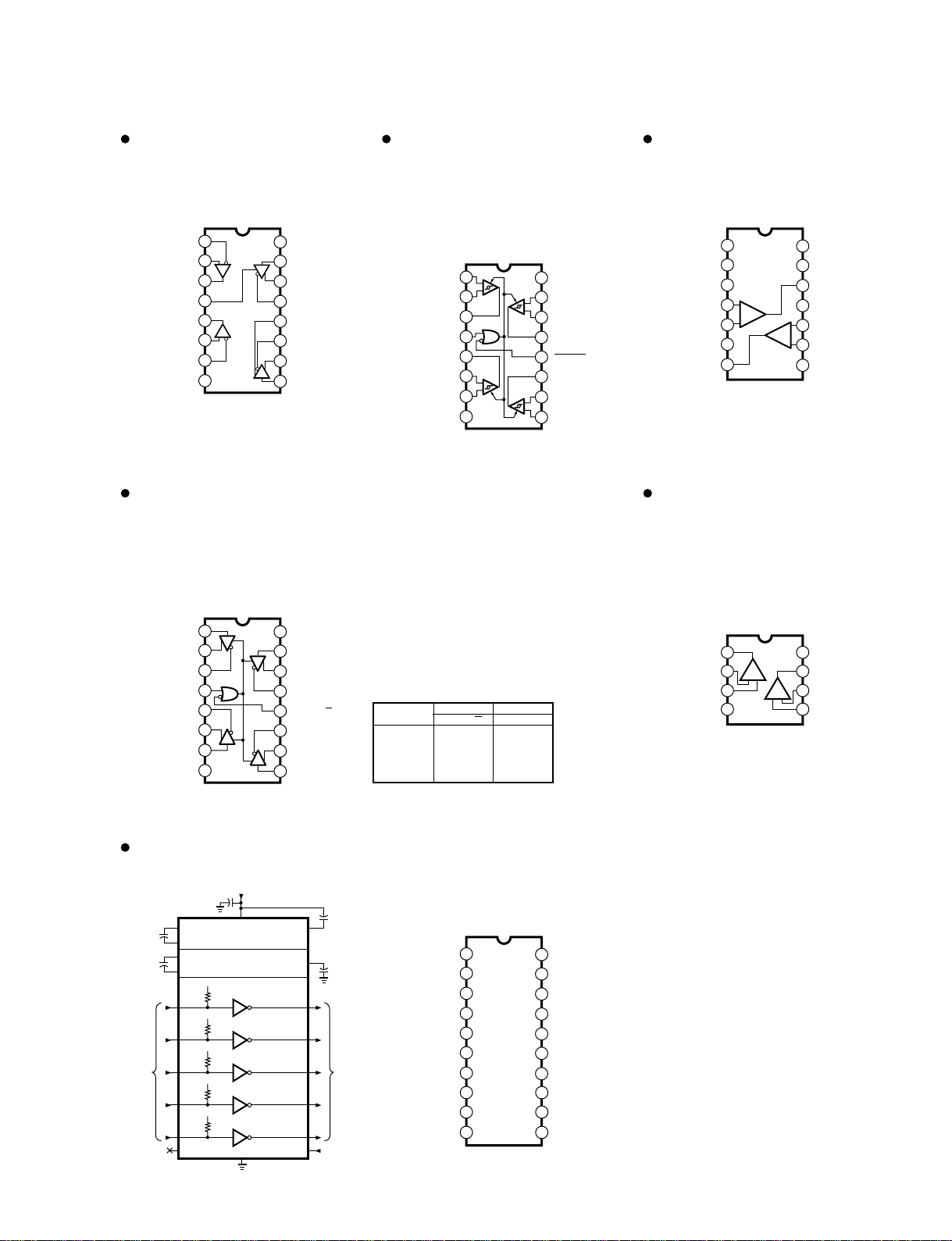
18
SN74HC125N (IR012550)
HD74LV125AFPEL (IS012500)
Quad 3-State Bus Buffer
CIB:
JK:
SN74LV138ANSR (IS013810)
3 to 8 Demultiplexer
CIB: IC152
SN74LV139ANSR (IS013910)
Dual 2 to 4 Demultiplexer
JK1:
JK3:
HD74LV244AFPEL (IS024400)
Octal 3-State Bus Buffer
IDB: IC855
HD74LV245AFPEL (IS024500)
TC74VHC245F (XT487A00)
TC74VHCT245AF (XV242A00)
TC74HC245AP (IR024500)
Octal 3-State Bus Transceiver
CIB:
EDB:
EMB:
GDB:
IDB:
IFC1:
JK1:
JK2:
JK3:
JK5:
JK4:
JK6:
PDB:
HD74LV273AFPEL (IS027300)
SN74HC273N (IR027350)
Octal D-Type Flir Flop
CIB:
JK2:
JK4:
SN75121NSR (XU816A00)
Dual Line Driver
JK6: IC200
SN75124NSR (XV930A00)
Triple Line Receiver
JK6: IC201
1
2
3
4
5
6
7
A
A
Select
Enable
Output
Output
B
B
C
C
G2A
G2A
G2B
G2B
G1
G1
Y7
Y7 Y5
Y4
Y3
Y2
Y1
Y0
Y6
16
15
14
13
12
11
10
Vcc
YO
Y1
Y2
Y3
Y4
Y5
8
GND
9
Y6
1
2
3
4
5
6
7
1G
1A
1B
1Y0
1Y1
1Y2
1Y3
A
G
B
Y0
Y1
Y2
Y3
16
15
14
13
12
11
10
Vcc
2G
2A
2B
2Y0
2Y1
2Y2
8
GND
9
2Y3
Y2
Y3
Y1
Y0
B
A
G
1
2
3
4
5
6
7
C1
A1
Y1
C2
A2
Y2
GND
14
13
12
11
10
9
8
Vcc
C4
A4
Y4
C3
A3
Y3
1G
1A1
2Y4
1A2
2Y3
1A3
2Y2
1A4
2Y1
1 20
2 19
3 18
4 17
5 16
6 15
7 14
8 13
9 12
10 11
VDD (Vcc)
2G
1Y1
2A4
1Y2
2A3
1Y3
2A2
1Y4
2A1
(GND) Vss
1
2
3
4
5
6
7
20
19
18
17
16
15
14
Vcc
G
B1
B2
B3
B4
B5
B6
B7
B8
8
9
10
12
11
GND
A8
A7
A6
A5
A4
A3
A2
A1
D1R
13
1A
1B
2R
2S
2A
2B
2Y
GND
1 16
2 15
3 14
4 13
5 12
6 11
7 10
8 9
Vcc
1S
1R
1Y
3A
3S
3R
3Y
Vcc
2F
2E
2A
2Y
GND
1Y
2C
2B
2D
1A
1B
1C
1D
1E
1F
8
1
2
3
4
5
6
7
9
16
15
14
13
12
11
10
IC148,150
IC107
EMB: IC149
IC125
IC131
IC125
IC124
JK2:
JK4:
IC105-110,120,121,130,135,137,140,145,146
IC101,250-253,255-260,306,307,600-606
IC120-104,109,112,115,128,134,137-147
IC102,220-229,303,304,850-871
IC220-232,253,254,850-854,856-863,900-913,IC102
IC504-507,509,608-610,701-717
IC122-124,128-133
IC122-124,128-134
IC115,116,127-129,132,134-138
IC103,104,105
IC122,123,127-134
IC103,104,103,204
IC105,103,110-112,200-202,204-206,503,504,
800-822,850-872,900-904
CLEAR
1Q
1D
2D
2Q
3Q
3D
4D
4Q
GND
VCC
8Q
8D
7D
7Q
6Q
6D
5D
5Q
CLOCK
1 20
2 19
3 18
4 17
5 16
6 15
7 14
8 13
9 12
10 11
Q
DCK
CL
D
Q
CK
CL
Q
DCK
CL
D
Q
CK
CL
D
Q
CK
CL
Q
DCK
CL
D
Q
CK
CL
Q
DCK
CL
IC124
IC127
IC126
EMB:
JK3:
JK5:
IC136
IC117-119,133
IC102
JK1: IC127
Page 23
DSP1D
19
SN75C1168N (XU463A00)
Line Driver / Receiver
JK5: IC101
DS26C32ATMX (XU815A00)
Quad Differential Line Receiver
JK1:
JK2:
JK3:
JK4:
1
2
3
4
5
6
7
INPUT A
INPUT A
OUTPUT A
OUTPUT C
INPUT C
INPUT C
GND
ENABLE
16
15
14
13
12
11
Vcc
INPUT B
INPUT B
OUTPUT B
ENABLE
OUTPUT D
INPUT D
8
9
10
INPUT D
+
-
-
+
+
-
+
AM26LS31CNSR (XU996A00)
Quad Line Driver
JK1:
JK2:
JK3:
JK4:
1
2
3
4
5
6
7
1A
1Y
1Z
2Z
2Y
2A
GND
ENABLE G
16
15
14
13
12
11
Vcc
4A
4Y
4Z
ENABLE G
3Z
3Y
8
9
10
3A
H= high level
L= low level
X= irrelevant
Z= high impedance (off)
OUTPUTSENABLESINPUT
A
GGYZ
H
H
X
X
L
X
X
L
L
H
H
L
H
L
Z
L
H
L
H
Z
H
L
H
L
X
µPC319C (IG086700)
Voltage Comparator
JK5: IC100
NJM2082M (T1) (XN797A00)
NJM4560D (IG040000)
Dual Operational Amplifier
EMB:
JK5:
1
2
3
4
5
6
7
NC
NC
GND1
+INPUT1
-INPUT1
-V
OUTPUT2
14
13
12
11
10
9
8
NC
OUTPUT1
OUTPUT1
+V
-INPUT2
+INPUT2
GND2
+
+
-
MAX202CSE (XP113A00)
RS-232C Transceiver
JK6: IC102
1
2
3
4-V
8
7
6
5
Output A +V
Non-Inverting
Input A
-DC Voltage Supply
+DC Voltage
Supply
Output B
Inverting
Input B
Non-Inverting
Input B
Inverting
Input A
+-
+-
1
2
3
4
5
6
7
5
6
7
5
6
7
T3 OUT
T1 OUT
T2 OUT
T2 IN
T1 IN
GND
Vcc
C1+
V+
C1–
14
13
12
11
10
9
8
T4 OUT
T5 IN
N.C.
SHDN
T5 OUT
T4 IN
T3 IN
V–
C2–
C2+
+
+
+5V INPUT
0.1uF
0.1uF
6.3V
+
0.1uF
16V
0.1uF
6.3V
9
13
25
8
10
V+
V–
Vcc
+5V TO +10V
VOLTAGE DOUBLER
+10V TO –10V
VOLTAGE INVERTER
C1+
C1–
C2+
C2–
+
0.1uF
16V
11
12
+
+5V
400K
T1
T1 OUTT1 IN
34
+5V
400K
T2 OUTT2 IN
114
+5V
400K
T3 OUTT3 IN
2015
+5V
400K
T4 OUTT4 IN
16
17
19
6
18
+5V
400K
T5 OUTT5 IN
SHDN
GND
N.C.
RS-232
OUTPUTS
TTL/CMOS
INPUTS
T2
T3
T4
T5
1
2
3
4
5
6
7
1B
1A
1R
1DE
2R
2A
2B
16
15
14
13
12
11
10
Vcc
1D
1Y
1Z
2DE
2Z
2Y
8
GND
9
2D
IC103-107,113-117
IC104,116
IC101,102,104-106,125
IC103-105,113-115
IC108,118
IC103,105-108,115,117-120
IC107,120-124
IC106-108,116,117
IC121
IC106
Page 24
DSP1D
20
DP8392CN (XW278A00)
CTI
JK5: IC201,301,401,501
1
2
3
CD+
RX+
4VEE
5VEE
6RX–
TX+
TX–
7
CD–
16
15
14
CDS
RXI
13 VEE
12 RR–
11 RR+
10
8 9
GND
HBE
TXO
COAX
CABLE
RXI
CDS
HBE
TXO
GND
DATE
BUFFER
SENSE
BUFFER
RECEIVER
EQUALIZER
AND AMPLIFIER
4-POLE BESSEL
LOW PASS FILTER
4-POLE BESSEL
LOW PASS FILTER
HEARTBEAT
GENERATOR
JABBER
TIMER
TRANSMITTER
SQUELCH
TRANSMITTER
RECEIVER
AC-DC SQUELCH
DIFF LINE DRIVER
DTE INTERFACE
RECEIVE
PAIR
(RX–, RX+)
COLLISION
PAIR
(CD–, CD+)
TRANSMIT
PAIR
(TX–, TX+)
DIFF
LINE
DRIVER
Vcc
MHz
OSCILLATOR
–
+
COLLISION
COMPARATOR
+–
Vch
Page 25
DSP1D
INSPECTION
1. Range of Application
These specifications apply to the DSP1D and DSP1D-EX.
2. Preparations
2-1. Conditions
For details on the connection method, refer to the Test Program Specifications KES-92651.
The function generator used for inspection must be the Sony Tektronix AFG310 or equivalent. When using the AFG310, the
settings are as follows.
FUNC :PULS
MODE :CONT
MODUL :OFF
AMPL :1.800
OFFSET :0.900
Unless otherwise specified, the conditions are as follows.
· The function generator BNC output is connected to WORD CLOCK IN (BNC).
· Set WORD CLOCK IN to 75 Ω.
2-2. Loading the Firmware
The firmware used must be the “CS1D Firmware” (managed with the already drawn CD-R assembly drawing (3JL-XY714A0) of
the FMID System Software matching the version on the cover sheet. For details on the firmware writing method, refer to the Test
Program Specifications KES-92651.
2-3. Test Program
For details on the starting method etc., refer to the Test Program Specifications KES-92651.
2-4. Jigs
The altered jigs and cable circuit diagram are shown from Page 47 of the Test Program Specifications KES-92651.
3. Inspection
3-1. Inspection with Test Program
· Inspect based on the Test Program Specifications KES-92651.
3-2. Jitter Measurement
· Connect the jitter meter to the WORD CLOCK OUT terminal.
· Set the function generator to 48 kHz and 44.1 kHz, connect to WORD CLOCK IN, and measure the jitter with the jitter meter.
Range of tolerance
48 kHz
44.1 kHz
3-3. Fan Operation Check
· Check that the fan rotates while the power is on.
3-4. Sound
· For the connections and settings, refer to the Test Program Specifications.
(1) Fs = 51.12 kHz (48 kHz + 6.5 %)
· Set the function generator to 51.12 kHz.
· Test listen for 30 seconds and verify that there is no noise.
6 ns max.
5 ns max.
(2) Fs = 39.69 kHz (44.1 kHz -10 %)
· Set the function generator to 39.69 kHz.
· Test listen for 30 seconds and verify that there is no noise.
4. Factory Settings
· Rear panel.
WORD CLOCK IN 75 Ω: ON
42
Page 26
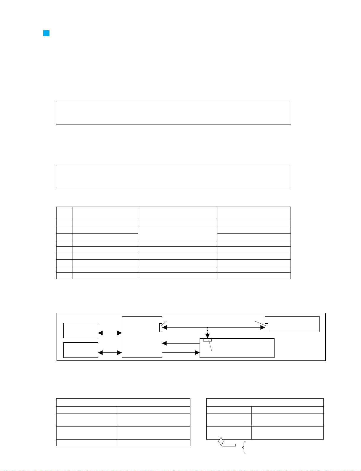
TEST PROGRAM
Serial connection
D-sub 9-pin
cross-cable
Ether cable
RS232C
RS232C
OUTPUT A
AI8
DSP1D
CS1D
INPUT A
AO8
INTPUT 1
One or the other
Only COM1 can be used.
OUTPUT 1
PC
(Windows 95 or later)
A. Preparations for Inspection
This equipment requires firmware. When there are changes to the manufacturing processes and program for this equipment, it is
necessary to write the new firmware to FlashRom from a PC. The software used and firmware used and their version numbers and
concrete details of the writing method are shown below.
•PM1DLOAD installation
First, it is necessary to install in the PC the dedicated software for writing the firmware. For the installation method, refer to the
CS1D Test Program Specifications.
Software used: PM1DLOAD within PM1D system software
Version used: PM1D system software component files with the version number listed on the cover sheet.
(Managed with the already drawn CD-R assembly drawing (3JL-XY714A0.)
•Writing the firmware
The sheets that require firmware downloading are CIB (the 2CPU portion of E_TUC/E_HIF), EMB (the 2CPU portion of
EMU/UIF), PDB, GDB, IDB (the 2CPU portion of DSP1D-EX), and EDB.
Below is the firmware used. Detailed procedures are on the following pages.
Firmware used: DSP1D firmware in PM1D system software
Version used: PM1D system software component files with the version number listed on the cover sheet.
(Managed with the already drawn CD-R assembly drawing (3JL-XY714A0.)
DSP1D
* If PM1DLOAD has been installed according to the instructions in the CS1D Test Program Specifications, the version
for the firmware above is taken care of and there is no need to worry about it.
Firmware name
1
2
3
4
5
6
7
8
9
EMU
E_TCU
E_HIF
UIF
PDB
GDB
IDB1
IDB2
EDB
“Firmware” and “subject sheet and subject connector” correspondence table
Sheet name
EMB
CIB
EMB
PDB
GDB
IDB (1st sheet)
IDB (2nd sheet)
EDB
Connection number for writing
firmware independently
CN104
CN105
CN107
CN105
CN100
CN100
CN100
CN100
CN100
•Method for writing firmware using the CS1D or DSP1D RS232C port
* It is possible to write the CPU firmware from the PC via the RS232C port. This is the method normally used.
1. Install and set PM1DLOAD with the method given in the CS1D Test Program Specifications.
2. Connect as in the figure above. Do not connect any other signal lines. However, to write firmware just to this equipment for a
manufacturing process with this equipment, the only configuration required is DSP1D and the PC.
3. Write the firmware to all the units listed in the CS1D Test Program Specifications. You can check the status of the LEDs on
each sheet. After the firmware has been written, check that the versions for all the units are the desired versions.
For PDB, GDB, IDB1, IDB2, and EDB
MONI-4 flashing Program not yet written
MONI-4 lit up
LED other than MONI-4 Program writing complete
flashing or lit up Program writing inhibited
All LEDs out Board defect possible
Program writing complete
Program writing enabled
LED flashing Program not yet written
LED lit up
LED off
Corresponding LEDs
For CIB, EMB
Program writing complete
Ready for program writing
Program writing complete
Not ready for program writing
CIB
(E_TCU: LD101, E_HIF: LD102)
EMB
(EMU: LD101, UIF: LD102)
43
Page 27
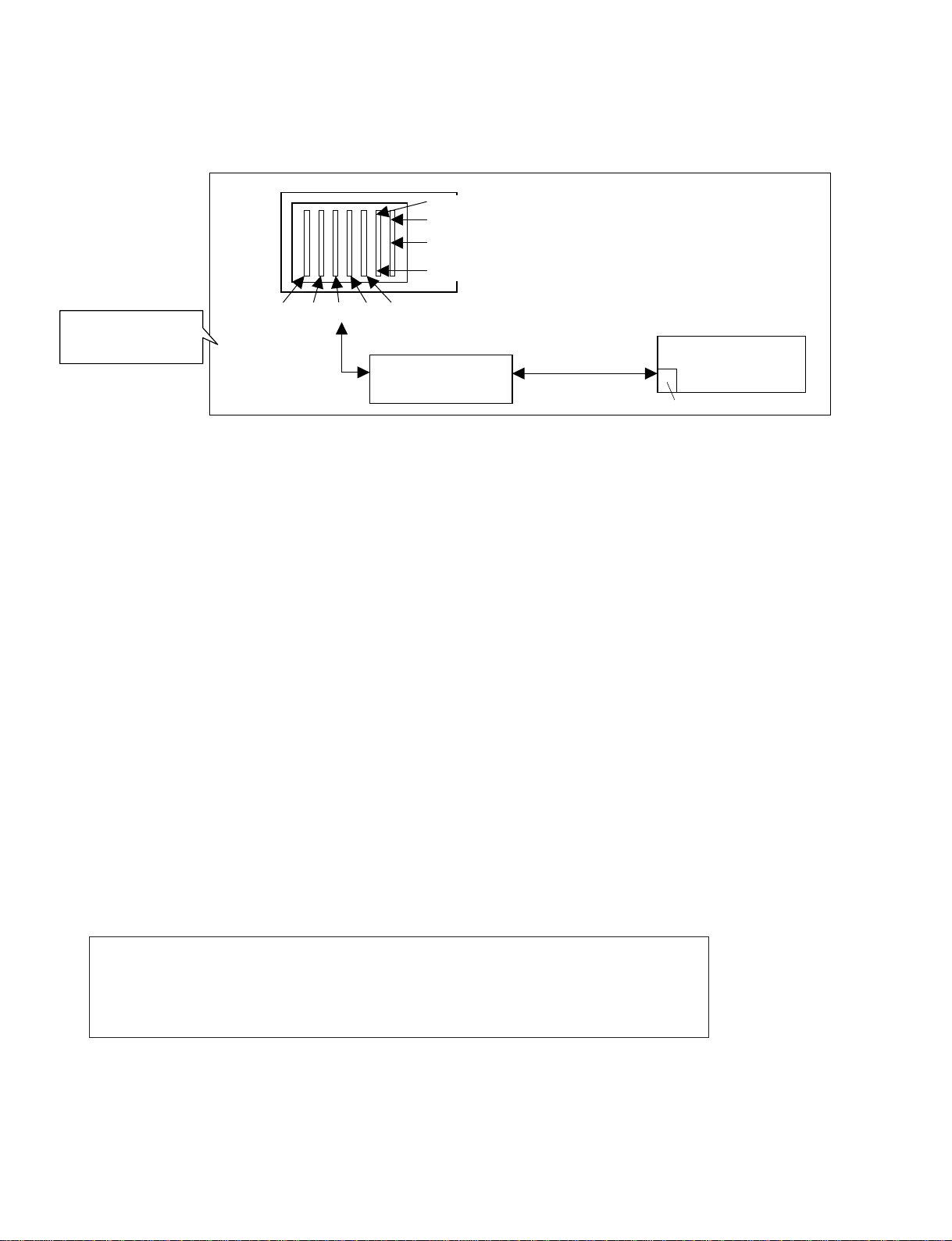
•Method for writing firmware directly to each sheet
* When there is some kind of problem and the firmware can not be written with the method on the previous page, use
the method below.
1. Install and set PM1DLOAD with the method given in the CS1D Test Program Specifications.
2. Remove the DSP1D front panel.
3. Remove all the CPU boards except the one on which you want to write PDB. (When writing to PDB, leave only that board.)
4. Connect the D-sub 9-pin serial cables (cross) and DSP-CHECK board between the 5-pin connector for the target board and the
PC. At this time, do not connect other signal lines.
• For PDB, GDB, IDB1, IDB2, and EDB
5. Short Pin 1 of the target CPU directly to ground.
6. With the connections still as in 4., switch on the power for the DSP1D. If the LED darkens momentarily, you can remove the short.
7. Check that the LED on the board is lit or flashing, indicating that the system is ready for writing. (See the previous page.)
8. After starting PM1DLOAD, select CardDirect with MODE SELECT, then press OK.
9. Press the Update button on the DSP1D.
10.Select the desired firmware, then press the Write button. (See Page 45.)
11.After writing ends, end PM1DLOAD.
12.Switch off DSP1D. Remove the PH connector, then switch the power for DSP1D on again and check that it starts up normally.
• For EMB, CIB
5. Switch on the power for the DSP1D.
6. Check that the LED on the board is lit or flashing, indicating that the system is ready for writing. (See the previous page.)
7. After starting PM1DLOAD, select CardDirect with MODE SELECT, then press OK.
8. Press the Update button on the DSP1D.
9. Select the desired firmware, then press the Write button. (See Page 45.)
10.After writing ends, end PM1DLOAD.
11.Switch off DSP1D. Remove the PH connector, then switch the power for DSP1D on again and check that it starts up normally.
•PM1D inspection PC software preparation
Inspection with this device uses special PC software for inspection.
The version of the software used is shown below.
For details of the preparation method and execution method, refer to the CS1D Test Program Specifications.
Refer to version.txt in the same directory as the firmware on Page 2 and input the version character string exactly as given there.
(For details on the input positions, refer to the "PM1D Inspection PC Software Summary" given later in this document.)
•Installing the USB driver for inspection
This equipment has a USB terminal. Therefore, it is necessary to install the USB driver for inspection in the inspection PC. The
files used are included in the above PM1D inspection PC software, so install with the following procedure.
DSP1D
44
To 5-pin PH connector
on each board (CPU)
(See Page 2.)
Only COM1 can be used.
PDB GDB IDB1 IDB2 EDB
For information on the DSP-CHECK board, refer
to the LMY-SLOT inspection jig specifications.
*
CIB(E_TCU)
CIB(E_HIF)
EMB(UIF)
EMB(EMU)
Use the cable for straight
connection between 5-pin
PH connectors
DSP1D
DSP-CHECK
(serial communications jig)
Serial connection
D-sub 9-pin cross-cable
PC
(Windows 95 or later)
Firmware used: PM1D inspection PC software in PM1D system software
Version used: PM1D system software component files with the version number listed on the cover sheet.
(Managed with the already drawn CD-R assembly drawing (3JL-XY714A0.)
* The operating systems supported are Windows 95/98.
* USB inspection is only supported in Windows 98. (Windows 98 Second Edition is not supported yet.)
Page 28
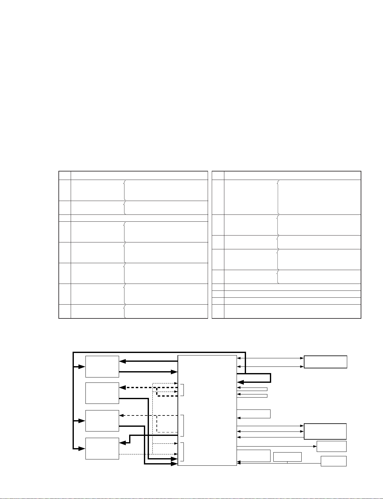
PC
Windows 95 or later
MIDI THRU
TC IN
Changed
USB
SERIAL
MIDI OUT
MIDI IN
GPI OUT
GPI IN
COMMUNICATION1
COMMUNICATION2
REMOTE
W.CLK I/O
Fixed
Fixed
DSP1D
INPUT 1-10
OUTPUT 1-6
CASCADE IN
CASCADE OUT
TO CONSOLE 1-2
68-pin port connections · Solid lines
· Dotted lines
·····
···
Fixed
Changed
Cascade
ID
change jig
Output
ID
change jig
TO CONSOLE
(output)
ID
change jig
Input
ID
change jig
D24
Jitter meter
oscilloscope
Func.
Generator
1. For the PM1D inspection PC software, start 16. DSP1D-JK6, LED2 Test.
2. When the pop-up box for connecting the USB cable is displayed, connect the USB cable.
3. After a short while, the system asks you to specify the driver. Specify the directory containing the PM1D inspection PC software.
4. The installation proceeds as indicated by the OS.
5. After installation is complete, press the OK button on the pop-up box that came up in 2.
6. If inspection is OK, the installation has completed normally.
* The only operating system supported is Windows98. The USB driver can not be used with Windows 98 Second Edition.
* The USB port is only activated in the state in 2. Beware. If you insert the USB cable in any other state, it is not
correctly recognized by the PCS1De and the wrong driver is installed.
* Once the driver has been installed, the above procedure is not necessary for USB tests.
* This driver is only for inspection. It does not add the DSP1D USB function.
* The CS1D inspection USB driver must be installed separately.
B. Inspection Method
The inspection items are given below. Except for 17., these items are inspected using the PM1D inspection PC software. For details
on each item, see from Page 51 on.
C. Inspection Using PM1D Inspection PC Software
Except for the all-group sound test, the inspections use the PM1D inspection PC software to control the DSP1D and the inspection is
carried out autonomously. The inspection configuration diagram is as follows.
DSP1D
45
1
2
3
4
5
6
7
8
No.
CIB Test 1-1. TCU
1-2. HIF
1-3. CIF
EMB Test 2-1. EMU
2-2. UIF
IFC Test
PDB Test 4-1. CPU
4-2. DSP6
4-3. DSP5
GDB Test 5-1. CPU
5-2. DSP6
5-3. DSP5
IDB1 Test 6-1. CPU
6-2. DSP6
6-3. DSP5
IDB2 Test 7-1. CPU
7-2. DSP6
7-3. DSP5
EDB Test 8-1. CPU
8-2. DSP6
Items
9
10
11
12
13
14
15
16
17
No.
Connection test 9-1. PDB
9-2. GDB
9-3. IDB1
9-4. IDB2
9-5. EDB
JK1 (INPUT x) Test 10-1. INPUT 1
:
10-10.INPUT 10
JK4 (TO CONSOLE x)
11-1. TO CONSOLE 1
INPUT Test 11-2. TO CONSOLE 2
JK2 (OUTPUT x) Test
12-1. OUTPUT 1
:
12-6. OUTPUT 6
JK4(TO CONSOLE x)
13-1. TO CONSOLE 1
OUTPUT Test 13-2. TO CONSOLE 2
JK3 (CASCADE) Test
JK5 Test
JK6 , LED2 Test
All-group sound inspection
(Inspects using DSP1D sound inspection data. See Page 49.)
Items
Page 29
ON
SW 101
12345678
Input ID change jig
[INPUT 1-10]
[TO CONSOLE (INPUT)]
ON
SW 102
12345678
ON
12345678
ON
12345678
ON
12345678
ON
12345678
ON
12345678
SW 101
Output ID change jig
[OUTPUT 1-6]
SW 102
ON
12345678
SW 101
Cascade ID change jig
[for CASCADE IN check]
SW 102
SW 101
Cascade ID change jig
[for CASCADE OUT check]
SW 102
TO CONSOLE (OUTPUT)
ID change jig
[TO CONSOLE (OUTPUT)]
The ID is not inspected at TO CONSOLE (OUTPUT), so the DIP switch settings do
not matter. Connect the altered ID change jig just for TO CONSOLE (OUTPUT).
(For details on the alteration, refer to the DSIP Overall Inspection Specifications.)
DSP1D
46
For details on inspecting with this software, see from Page 51 on.
Locations with instructions for changes have instructions for that inspection item in the PC software, so change the connections
according to the instructions.
(* Even if the system is the DSP1D not the DSP1D-EX, inspect with IDB2 inserted for the bus check.)
For time code output, insert an MO disc (song data or the like) that can idle as long as possible. Also, switch On MMC Receive on
the Utility menu and set TC Select to Serial IN on the Setup menu.
In the 16 JK6 inspection, it is necessary to change the BNC cable. The connection method is as follows.
* Since the input and output functions are inspected separately for TO CONSOLE, there are two connection methods.
* There are three special 68-pin port ID change jigs (for INPUT, OUTPUT, and CASCADE) but these are the same jig
with just the DIP switch settings changed. In other words, you can work with just one ID change inspection jig by
changing the DIP switch settings appropriately. For information on the ID change jig, refer to the LMY-SLOT inspection
jig specifications.
D24 setting method
W. CLK connection method
68-pin port connection method table
ID change jig DIP switch settings
IN 48 kHz + 6 %
IN 44.1kHz - 10 %
Jitter 48 kHz
Jitter 44.1 kHz
IN/OUT
JK6-W.CLK inspection sub-item
W.CLK In ········ Connect the function generator and output the clocks.
W.CLK Out ····· No need to connect
W.CLK In ······· Connect the function generator and output the clocks.
W.CLK Out ····· Connect the jitter meter and measure.
Loopback connection between W.CLK Out and W.CLK In
Connection method
10. INPUT 1-10
11. TO CONSOLE
(INPUT) 1-2
12. OUTPUT 1-6
13. TO CONSOLE
(OUTPUT) 1-2
14. CASCADE IN/OUT
Input ID change jig
Output ID change jig
Altered ID change jig just for
TO CONSOLE (OUTPUT)
Cascade ID change jig
Necessary jigInspection item
To INPUT 1-10
To OUTPUT x
To Console 1-2
To INPUT x To OUTPUT 1-6
Connected TO CONSOLE 1-2 and INPUT; no polarity.
To CASCADE IN To CASCADE OUT
ID change jig connection method
From left side (CN103) From right side (CN102)
Page 30
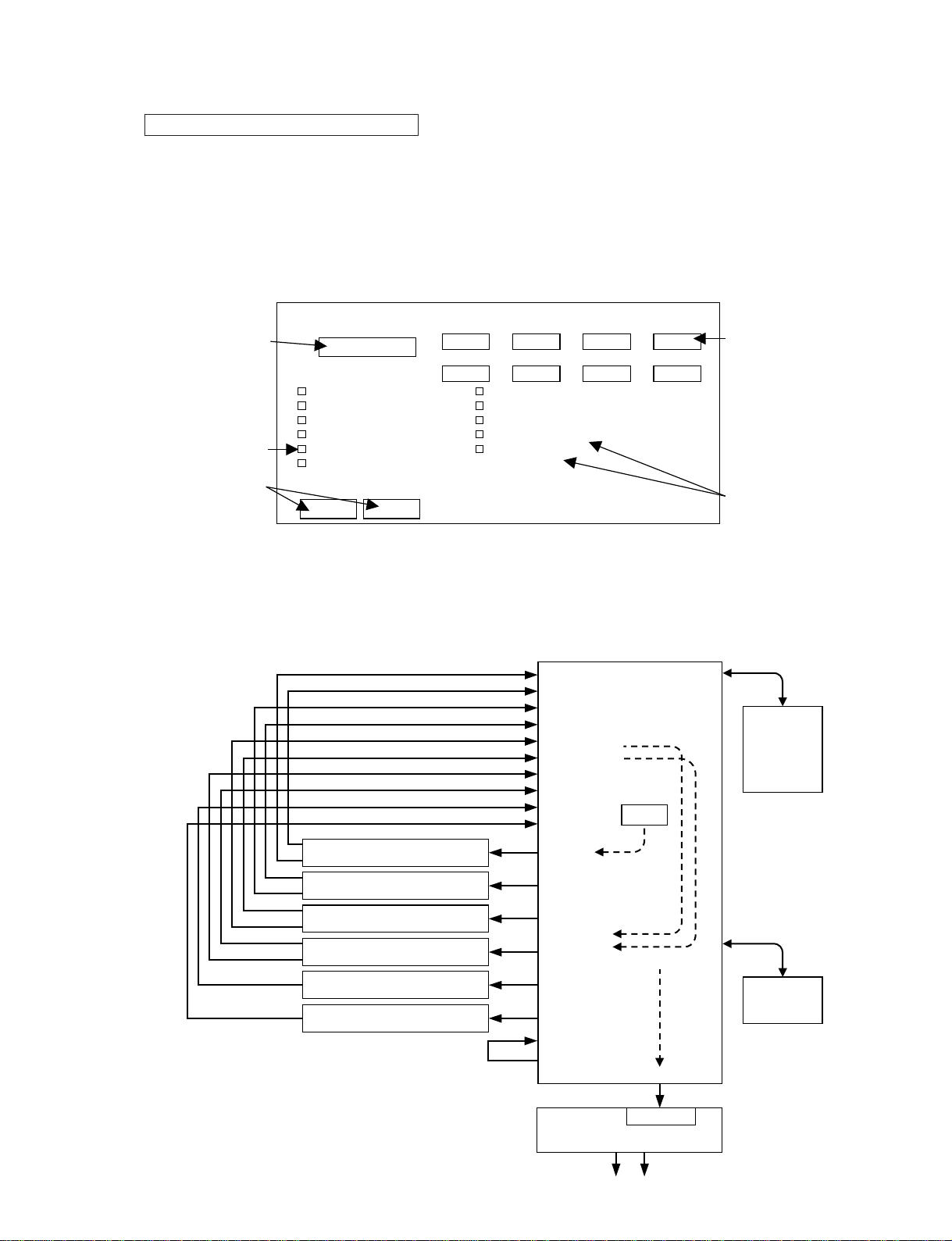
OUTPUT1
INPUT1
OUTPUT2
OUTPUT3
OUTPUT4
OUTPUT5
OUTPUT6
INPUT2
INPUT3
INPUT4
INPUT5
INPUT6
INPUT7
INPUT8
INPUT9
INPUT10
CONSOLE I/O
CASCADE IN
CASCADE OUT
DIRECT
OUT
DSP1D
PC
Windows 95
or later
RS232C
RS232C
Altered ID change jig A (1 in 2 out)
Altered ID change jig A (1 in 2 out)
Altered ID change jig A (1 in 2 out)
Altered ID change jig A (1 in 2 out)
Altered ID change jig B (1 in 1 out)
Altered ID change jig B (1 in 1 out)
* ID change jigs A/B are altered versions that set the IDs for input and
output separately.
The AI8 IDs are output to the input connection terminals.
The AO8 IDs are output to the output connection terminals.
* ID change jig A gathers two ID change jig Bs in 1 input; the outputs
are distributed simply in parallel, so the 2-output side connections
can be either even or the odd input terminals.
* Connect 01V using an MIO card altered to output the console ID.
(Refer to the DSP1D Overall Inspection Specifications.)
Function
Generator
BNC
Repeat
OSC
Final output
01V
Altered MIO
Inspected auditorily.
DSP1D F/W Latest Version
CIB(TCU)
xxxxxx
CIB(HIF)
xxxxxx
EMB(EMU)
xxxxxx
EMB(UIF)
xxxxxx
PDB
xxxxxx
GDB
xxxxxx
IDB
xxxxxx
EDB
xxxxxx
Pressing this button automatically starts the check
of the item to be checked.
Input the latest firmware version.
When the version is checked,
this character string and the
version actually written in the
firmware are compared. The
value entered here is retained
in memory.
The check items and check results are displayed. Pressing
a check item button enables
inspection of only that item.
Only items whose checkboxes are checked are automatically checked.
ALL checks all the items.
CLEAR removes all the
checks.
Auto Test Start
ALL CLR
1-1.
1-2.
1-3.
2-1.
2-2.
3.
CIB (TCU)
CIB (HIF)
CIB (CIF)
EMB (EMU)
EMB (UIF)
IFC Test
OK
OK
OK
OK
OK
:
OK
4-3.
5-1.
5-2.
5-3.
PDB (DSP5)
GDB (CPU)
GDB (DSP6)
GDB (DSP5)
OK
OK
OK
OK
6-1.
IDB1 (CPU)
:
:
OK
Version character string input column
DSP1D
47
Except for Item 17., the PM1D is inspected using PC inspection software. This inspection software is common for
AI8/AO8/DSP1D/CS1D.
For details on the basic operation methods, menu screen specifications, etc., refer to the CS1D Test Program Specifications.
The DSP test menus are shown below.
Before the inspection, the latest version of each piece of DSP1D software must be input. (This is necessary for the version check.)
For the version character string to be input, refer to version.txt in the same directory as the DSP1D firmware.
The following pages give details on each check item and how the PC software handles it.
PM1D inspection PC software summary
D. All-Group Sound Inspection
After all the inspections were carried out with the PM1D inspection PC software, the sound inspection is carried out.
After making the connections as in the diagram below, inspect with the procedure given from the next page on. Note that the altered
ID change jigs A/B are separate from the dedicated TO CONSOLE (OUTPUT) altered ID change jig. (If multiple ID change jigs can
be not be made available, substitute with the method given later in this document.)
Page 31

DSP1D
48
•Method using six altered ID change jigs (This is the method normally used.)
1. Connect according to the connection diagram. Supply a 48kHz clock from the function generator.
2. Execute the PM1D Manager for Windows from the PC. From Utility - LOAD/SAVE, execute the DSP1D sound and LOAD the
inspection data. (For the version, installation method, usage method, etc., see below.)
3. Set ENGINE A to W.CLOCK IN with SYS/W.CLOCK - WORD CLOCK.
4. Set OSC OUT to 1AO8:1-1 with MON/CUE - OSCILLATOR, set ON. OSC to IN, then adjust the level.
5. Recall SCENE 00.1: SOUND THRU1 with SCENE - MEMORY.
6. Set the switch for the altered MIO connected to 01V to ST.
7. Check the audio through 01V.
8. Set the switch for the altered MIO connected to 01V to ST.
9. Check the audio through 01V.
•Method using only one altered ID change jig
1. Connect according to the connection diagram. Supply a 48kHz clock from the function generator.
2. Connect an altered ID change jig to INPUT 1 and 2 and OUTPUT 1.
3. Execute the PM1D Manager for Windows from the PC. From Utility - LOAD/SAVE, execute the DSP1D sound and LOAD the
inspection data. (For the version, installation method, usage method, etc., see the previous page.)
4. Set ENGINE A to W.CLOCK IN with SYS/W.CLOCK - WORD CLOCK.
5. Set OSC OUT to 1AO8:1-1 with MON/CUE - OSCILLATOR, set ON. OSC to IN, then adjust the level.
6. Recall SCENE 00.1: SOUND THRU1 with SCENE - MEMORY.
7. Set the switch for the altered MIO to ST and check the audio through 01V.
8. Set the switch for the altered MIO to MON and check the audio through 01V.
9. Recall SCENE 00.2: SOUND THRU2 with SCENE - MEMORY. Check that the audio goes off.
10.Change the input side connections only to INPUT 3 and 4.
11.Repeat *1.
12.Recall SCENE 00.3: SOUND THRU3 with SCENE - MEMORY. Check that the audio goes off.
13.Change the input side connections only to INPUT 5 and 6.
14.Repeat *1.
15.Recall SCENE 00.4: SOUND THRU4 with SCENE - MEMORY. Check that the audio goes off.
16.Change the input side connections only to INPUT 7 and 8.
17.Repeat *1.
18.Recall SCENE 00.5: SOUND THRU5 with SCENE - MEMORY. Check that the audio goes off.
19.Change the input side connections only to INPUT 9 and 10.
20.Repeat *1.
21.Set OSC OUT to 2AO8:1-1.
22.Change the output side connection only to OUTPUT 2. (The INPUT remains 9 and 10 and the scene 00.5.)
23.Repeat *1.
24.Set OSC OUT to 3AO8:1-1.
25.Change the output side connection only to OUTPUT 3.
26.Repeat *1.
27.Set OSC OUT to 4AO8:1-1.
28.Change the output side connection only to OUTPUT 4.
29.Repeat *1.
30.Set OSC OUT to 5AO8:1-1.
31.Change the output side connection only to OUTPUT 5.
32.Repeat *1.
*1
{
Software used: PM1D Manager for Windows within PM1D system software
Version used: PM1D system software component files with the version number listed on the cover sheet.
(Managed with the already drawn CD-R assembly drawing (3JL-XY714A0.)
* The installation method is the same. Refer to install.txt in the PM1D system software.
Data used: DSP1D sound inspection software within PM1D system software
Version used: PM1D system software component files with the version number listed on the cover sheet.
(Managed with the already drawn CD-R assembly drawing (3JL-XY714A0.)
* Start the installed PM1D Manager for Windows, then read with UTILITY - LOAD/SAVE.
Page 32

1-1. DSP1D-CIB
(TCU-IC129) Test
This test checks around the CIB TCU.
Check item
ID TCU [11h]
RAM
• Data Bus 16bit(15-0)
• Address Bus 20bit(19-0)
Flash (Check Sum)
Version
DPM
• EM BUS<->TC BUS R
1-2. DSP1D-CIB
(TCU-IC129) Test
This test checks around the CIB HIF.
1-3. DSP1D-CIB (ETC)Test
This test makes other checks of the CIB.
Check item
FPGA HIF [02h]
DPM
• EMU<->CONS L
FIFO
TC IC
Check item
ID TCU [12h]
RAM
• Data Bus 16bit(15-0)
• Address Bus 20bit(19-0)
Flash (Check Sum)
Version
DPM
• HI BUS<->EM BUS L
DSP1D
49
33.Set OSC OUT to 6AO8:1-1.
34.Change the output side connection only to OUTPUT 3.
35.Repeat *1.
1. DSP1D-CIB Test
This test checks the DSP1D-CIB. It checks the following items. Those items for which there are figures display the results in
binary. Detailed screen output specifications are given on the following pages.
The details for 1-2. are omitted because they are the same as for 1-1.
* For the DPM (dual port RAM) item, EM BUS <-> TC BUS R etc. is written. This indicates which of the DPM buses is
inspected. For example, for EM BUS <-> TC BUS R, this indicates the check of the TC BUS side seen from the DPM
(right side for the DPS BUS <-> CM BUS notation).
* RAM OK
DataBus
AddressBus
* DPM
EM BUS <-> TC BUS R
* Flash
* Version
OK
OK
OK
1-1. DSP1D-CIB (TCU-IC129) Test
OK
1-1. DSP1D-CIB (TCU-IC129) Test
OK
RAM(IC133): OK
Flash(IC132):
Version:
OK
OK
DPM: OK
OK
Now Checking …
DPM
NG example
* ID TCU [11h]
ID: TCU[11h]
* RAM NG
DataBus
AddressBus
* DPM
EM BUS <-> TC BUS R
* Flash
* Version
NG
NG
NG
1-1. DSP1D-CIB (TCU-IC129) Test
1-1. DSP1D-CIB (TCU-IC129) Test
NG
RAM(IC133): NG
Flash(IC132):
Version:
NG
NG
DPM: NG
NG
* ID xxx [xxh]
ID: xxx [xxh]
DBus[38-35,32-29,16-13,10-7 pin]
CheckSum = xxxx[xxxx]
Current = x.xx , Latest = x.xx
EM BUS <-> TC BUS R:
NG
11111111 11111111
ABus[18-21,24-27,42-44,1-5 pin] NG
NG
1 11111111 1111111-
1-1. DSP1D-CIB (TCU) Test
This test checks around the CIB TCU.
OK/NG display for the page as a whole
Displayed when all the checks have been completed.
If OK, sub-items are
not displayed.
Sub-item
Received ID displayed as
board name and hexadecimal
OK/NG display for
individual items
The NG is displayed the
moment the item is
found to be NG, even if
the test is still underway.
If there is no response
from the firmware,
"NO" is displayed.
Displays all the detailed results so
far. This display can be scrolled.
Current status display
Corresponding IC number
Corresponding pin number
Stopped the moment an
actual ID NG appears;
stopped at the end of the
page for any other NG.
Main item
Checked in order from top to bottom.
Completed main items have marks
next to them.
SRAM OK: LED lit up
NG: LED flashes on (0.2 s) - Off (0.2 s) - On (0.2 s) - Off (0.1 s)
Flash OK: LED lit up
NG: LED flashes on (0.1 s) - Off (0.1 s) - On (0.1 s) - Off (0.1 s)
()
Terminal status display
Delimited in units of 8
digits right justified in the
order upper then lower.
0: Normal 1: Abnormal
-: Ignored
Gives the current version
and the latest version
Abnormal port name
Previously read value.
[ ] gives the correct value.
4-digit hexadecimal notation
Page 33

DSP1D
50
* DPM
* FPGA
OK
EMU <-> CONS L
* FIFO
* TC IC
OK
OK
1-3. DSP1D-CIB (ETC) Test OK
1-3. DSP1D-CIB (ETC) Test
OK
DPM: OK
FIFO(IC118,119,122,123):
TC IC(IC136):
OK
OK
OK
Now Checking …
TC IC
NG example
FPGA(IC126):
NG
* DPM
* FPGA
NG
EMU <-> CONS L
* FIFO
* TC IC
NG
NG
1-3. DSP1D-CIB (ETC) Test
1-3. DSP1D-CIB (ETC) Test
NG
NG
FIFO(IC118,119,122,123):
TC IC(IC136):
NG
NG
FPGA(IC126):
NG
DPM:
EMU<->CONS L(IC116):
SRAM OK: LED lit up
NG: LED flashes on (0.2 s) - Off (0.2 s) - On (0.2 s) - Off (0.1 s)
Flash OK: LED lit up
NG: LED flashes on (0.1 s) - Off (0.1 s) - On (0.1 s) - Off (0.1 s)
()
1-3. DSP1D-CIB (ETC) Test
This test checks around the CIB ETC.
* FPGA
* DIR2
OK
3. DSP1D-IFC Test OK
3. DSP1D-IFC Test
OK
FPGA(IC503): OK
OK
Now Checking …
FPGA
NG example
DIR2(IC604,605,606):
* FPGA
* DIR2
NG
3. DSP1D-IFC Test
3. DSP1D-IFC Test
NG
FPGA(IC503): NG
NG
DIR2(IC604,605,606):
3. DSP1D-IFC (TCU) Test
This test checks the IFC board.
2-1. DSP1D-EMB
(EMU-IC114) Test
This test checks around the EMB EMU.
Check item
ID EMU [10h]
RAM
• Data Bus 16bit(15-0)
• Address Bus 20bit(19-0)
Flash (Check Sum)
Version
DPM
• EM BUS<->DPM BUS L
• UI BUS<->EM BUS R
• HI BUS<->EM BUS R
• EM BUS<->TC BUS L
Battery
2-2. DSP1D-EMB
(UIF-IC127) Test
This test checks around the EMB HIF.
Check item
ID UIF [13h]
RAM
• Data Bus 16bit(15-0)
• Address Bus 20bit(19-0)
DPM
• UI BUS<->EM BUS L
Flash (Check Sum)
Version
2. DSP1D-EMB Test
This test checks the EMB. It checks the following
items. Those items for which there are figures
display the results in binary. Detailed screen output
specifications are given on the following pages.
The battery check item is only for 2-1. Here the
voltage is checked and if it is within the correct
range, OK is displayed. If it is NG, how far it
deviates from the correct value is displayed.
4. DSP1D-PDB Test
This test checks the DSP1D-PDB. It checks the following items. Those items for which there are figures display the results in
binary. Detailed screen output specifications are given on the following pages.
DSP6 total count···· 9
DSP5 total count···· 11
Page 34

DSP1D
51
4-1. DSP1D-PDB
(CPU-IC101) Test
This test checks around the PDB CPU.
Check item
ID PDB [14h]
RAM
• Data Bus 16bit(15-0)
• Address Bus 16bit(16-1)
• Data Bus 16bit(15-0)
• Address Bus 15bit(15-1)
Flash (Check Sum)
Version
DPM
4-2. DSP1D-PDB
(DSP6) Test
This test checks around PDB DSP6.
4-3. DSP1D-PDB (DSP5) Test
This test checks around PDB DSP5.
Check item
Chip Select
DSP5 <-> CPU
DSP6 -> DSP5
• Serial I/O
• Serial I/O
• Serial I/O
DSP5 -> DSP6
DPM
Check item
Chip Select
DSP6 <-> CPU
• Data Bus 16bit(15-0)
• Address Bus 7bit( 7-1)
DSP6 <-> DRAM
• Data Bus 32bit(31-0)
• Address Bus 10bit( 9-0)
DSP6 -> DSP6
• Serial I/O
• Data Bus 16bit(15-0)
• Address Bus
• ParallelI/O 32bit(31-0)
* RAM
* ID PDB [14h]
OK
AddressBus
* Flash
DataBus
* Version
* DPM
AddressBus
DataBus
00000000 0000000-
00000000 00000000
OK
4-1.
DSP1D-PDB (CPU-IC101) Test
OK
4-1. DSP1D-PDB (CPU-IC101) Test
OK
RAM(IC107): OK
Flash(IC114): OK
Version: OK
DPM: OK
OK
OK
NG example
ID: PDB [14h]
* RAM
* ID xxx [xxh]
NG
AddressBus
* Flash
DataBus
* Version
* DPM
AddressBus
DataBus
11111111 1111111-
11111111 11111111
NG
4-1.
DSP1D-PDB (CPU-IC101) Test
4-1. DSP1D-PDB (CPU-IC101) Test
NG
RAM(IC107): NG
Flash(IC114): NG
Version: NG
DPM: NG
NG
NG
ID: xxx [xxh]
Now Checking …
Version
DBus[xx-xx,xx-xx pin]
CheckSum = xxxx [xxxx]
Current = x.xx , Latest = x.xx
NG
NG
11111111 11111111
ABus[xx-xx,xx-xx pin]
1111 11111111 11111111
SRAM OK: LED lit up
NG: LED flashes on (0.2 s) - Off (0.2 s) - On (0.2 s) - Off (0.1 s)
Flash OK: LED lit up
NG: LED flashes on (0.1 s) - Off (0.1 s) - On (0.1 s) - Off (0.1 s)
()
4-1. DSP1D-PDB (CPU-IC101) Test
This test checks around the PDB CPU.
* DSP6 <-> CPU
* ChipSelect 0 00000000
0 00000000
0 00000000
OK
AddressBus
DataBus
* DSP6 <-> DRAM
0 00000000
0 00000000
OK
AddressBus
DataBus
* DSP6 <-> DSP6
xxx/xxx
OK
Serial I/O
4-2. DSP1D-PDB (DSP6) Test OK
4-2. DSP1D-PDB (DSP6) Test
OK
DSP6<->CPU: OK
DSP6<->DRAM: OK
DSP6 -> DSP6: OK
OK
NG example
ChipSelect:
NG
Now Checking …
DSP6 -> DSP6 No. xxx
ICxxx
NG
NG
* DSP6 <-> CPU
* ChipSelect 0 00100000
0 00101000
0 00001000
NG
AddressBus
DataBus
* DSP6 <-> DRAM
0 00000100
0 00000100
NG
AddressBus
DataBus
* DSP6 <-> DSP6
xxx/xxx
NG
Serial I/O
4-2. DSP1D-PDB (DSP6) Test
4-2. DSP1D-PDB (DSP6) Test
NG
DSP6<->CPU:
ABus[25-31 pin]
NG
NG
NG
DSP6<->DRAM: NG
DSP6 -> DSP6: NG
NG
ChipSelect:
DBus[34-43,47-52 pin]
DBus
[
151-144,142-135,130-123,121-114pin
]
11111111 11111111ICxxx
ICxxx
1111111-ICxxx
ABus[163-154 pin]
11 11111111
11111111 11111111
11111111 11111111ICxxx
SI/SO
11111111 11111111
- ICxxx
ICxxx - ICxxx, ICxxx
ICxxx[SOx] - ICxxx[SIx]
- ICxxx
4-2. DSP1D-PDB (DSP6) Test
This test checks around PDB DSP6.
Stopped the moment an actual
Chip Select or TxB NG appears;
stopped at the end of the page for
any other NG.
The DSP check results are displayed for each DSP. The DSPs are displayed
in order from the right of the ChipSelect signals on the circuit diagram.
(Blank: Not yet checked; 0: Normal; 1: Abnormal; N: No response)
Gives the abnormal
DSP IC number.
Display when a number of
checks are complete and there
have been a number of NGs
Displayed in binary in the order
Upper: 16 bits, Lower: 16 bits
The corresponding DRAM IC
number is also displayed.
IC number display for
both upper and lower
Displays from which
SO to which SI is NG.
Page 35

5-1. DSP1D-GDB
(CPU-IC100) Test
This test checks around the GDB CPU.
Check item
ID GDB [15h]
RAM
• Data Bus 16bit(15-0)
• Address Bus 16bit(16-1)
• Data Bus 16bit(15-0)
• Address Bus 15bit(15-1)
Flash (Check Sum)
Version
DPM
5-2. DSP1D-GDB
(DSP6) Test
This test checks around GDB DSP6.
Check item
Chip Select
DSP6 <-> CPU
• Data Bus 16bit(15-0)
• Address Bus 7bit( 7-1)
• Data Bus 32bit(31-0)
• Address Bus 10bit( 9-0)
DSP6 <-> DRAM
• Serial I/O
DSP6 -> DSP6
5-3. DSP1D-GDB
(DSP5) Test
This test checks around GDB DSP5.
Check item
Chip Select
DSP5 <-> CPU
• Data Bus 16bit(15-0)
32bit(31-0)
• Address Bus
DSP6 -> DSP5
• Serial I/O
• Serial I/O
DSP5 -> DSP6
• Serial I/O
• Parallel I/O
DSP5 -> DSP5
DSP1D
52
* DSP5 <-> CPU
* ChipSelect 000 000000
000 000000
000 000000
OK
AddressBus
DataBus
* DSP6 -> DSP5 OK
OK
* DSP5 -> DSP6
xxx/xxx
Serial I/O
xxx/xxx
Serial I/O
xxx/xxx
OK
Parallel I/O
* DSP5 -> DSP5
xxx/xxx
Serial I/O
4-3.
DSP1D-PDB (DSP5) Test
OK
4-3. DSP1D-PDB (DSP5) Test
OK
DSP5<->CPU: OK
DSP6 -> DSP5: OK
DSP5 -> DSP5: OK
OK
NG example
ChipSelect:
Now Checking …
DSP5 -> DSP6 No. xxx
NGDBus[xx-xx,xx-xx pin]
11111111 11111111ICxxx
* DSP5 <-> CPU
* ChipSelect 000 00000000
000 00010000
000 00000100
NG
AddressBus
DataBus
* DSP6 -> DSP5 NG
NG
* DSP5 -> DSP6
xxx/xxx
Serial I/O
xxx/xxx
Serial I/O
xxx/xxx
NG
Parallel I/O
* DSP5 -> DSP5
xxx/xxx
Serial I/O
4-3.
DSP1D-PDB (DSP5) Test
4-3. DSP1D-PDB (DSP5) Test
OK
DSP5<->CPU:
NGSI/SO
SI/SO
SI/SO
ICxxx[SOxx] – ICxxx[SIOxx]
NG
DSP6 -> DSP5:
NG
ICxxx[SIOxx] – ICxxx[SIxx]
NG
DSP5 -> DSP6:
NGABus[xx pin]
1-------ICxxx
NG
NG
ICxxx[SIOxx] – ICxxx[SIOxx]
PI/PO NG
ICxxx – ICxxx
[xx-xx,xx-xx pin] 11111111 11111111
[xx-xx,xx-xx pin] 11111111 11111111
DSP5 -> DSP5: NG
OK
ChipSelect:
4-3. DSP1D-PDB (DSP5) Test
This test checks around PDB DSP6.
For the DSP5 address bus, only
the upper bits can be checked.
The pins are written as SIxx
and SOxx, but for DSP5, they
are written as SIOxx.
Displays which pin numbers are NG between which DSPs. 16 are
displayed at a time.
The display is three digits, including the IC number display.
Basically, the same
as up till here
5. DSP1D-GDB Test
This test checks the GDB. It checks the following items. The specifications are basically the same as for 4-1. through 4-3.
DSP6 total count···· 13
DSP5 total count···· 7
6-1. DSP1D-IDB1
(CPU-IC100) Test
This test checks around the IDB1 CPU.
Check item
ID IDB1 [16h]
RAM
• Data Bus 16bit(15-0)
• Address Bus 16bit(16-1)
• Data Bus 16bit(15-0)
• Address Bus 15bit(15-1)
Flash (Check Sum)
Version
DPM
6-2. DSP1D-IDB1
(DSP6) Test
This test checks around IDB1 DSP6.
Check item
Chip Select
DSP6 <-> CPU
• Data Bus 16bit(15-0)
• Address Bus 7bit( 7-1)
• Data Bus 32bit(31-0)
• Address Bus 10bit( 9-0)
DSP6 <-> DRAM
• Serial I/O
DSP6 -> DSP6
6-3. DSP1D-IDB1
(DSP5) Test
This test checks around IDB1 DSP5.
Check item
Chip Select
DSP5 <-> CPU
• Data Bus 16bit(15-0)
• Address Bus
DSP6 -> DSP5
• Serial I/O
• Serial I/O
DSP5 -> DSP5
6. DSP1D-IDB1 Test
This test checks the IDB1. It checks the following items. The specifications are basically the same as for 4-1. through 4-3.
DSP6 total count···· 16
DSP5 total count···· 8
Page 36

9-1. DSP1D-Connection
(PDB) Test
Checks the connections between the PDB
and the other boards.
Check item
PDB -> IDB1
PDB -> IDB2
PDB -> GDB
PDB -> EDB
IDB1 -> PDB
IDB2 -> PDB
GDB -> PDB
EDB -> PDB
9-2. DSP1D-Connection
(GDB) Test
Checks the connections between the GDB
and the other boards.
Check item
GDB -> PDB
IDB1 -> GDB
IDB2 -> GDB
PDB -> GDB
EDB -> GDB
9-4. DSP1D-Connection
(IDB2) Test
Checks the connections between the IDB2
and the other boards.
Check item
IDB2 -> GDB
IDB2 -> PDB
IDB1 -> IDB2
PDB->IDB2
9-5. DSP1D-Connection
(EDB) Test
Checks the connections between the EDB
and the other boards.
Check item
EDB -> GDB
EDB -> PDB
PDB -> EDB
9-3. DSP1D-Connection
(IDB1) Test
Checks the connections between the IDB1
and the other boards.
Check item
IDB1 -> GDB
IDB1 -> PDB
IDB1 -> IDB2
PDB->IDB1
DSP1D
53
7-1. DSP1D-IDB2
(CPU-IC100) Test
This test checks around the IDB2 CPU.
Check item
ID IDB2 [16h]
RAM
• Data Bus 16bit(15-0)
• Address Bus 16bit(16-1)
• Data Bus 16bit(15-0)
• Address Bus 15bit(15-1)
Flash (Check Sum)
Version
DPM
7-2. DSP1D-IDB2
(DSP6) Test
This test checks around IDB2 DSP6.
Check item
Chip Select
DSP6 <-> CPU
• Data Bus 16bit(15-0)
• Address Bus 7bit( 7-1)
• Data Bus 32bit(31-0)
• Address Bus 10bit( 9-0)
DSP6 <-> DRAM
• Serial I/O
DSP6 -> DSP6
7-3. DSP1D-IDB2
(DSP5) Test
This test checks around IDB2 DSP5.
Check item
Chip Select
DSP5 <-> CPU
• Data Bus 16bit(15-0)
• Address Bus
DSP6 -> DSP5
• Serial I/O
• Serial I/O
DSP5 -> DSP5
7. DSP1D-IDB2 Test
This test checks the IDB2. It checks the following items. The specifications are basically the same as for 4-1. through 4-3.
DSP6 total count···· 16
DSP5 total count···· 8
9. DSP1D Connection Test
This test checks the connections among the PDB,
GDB, IDB1, IDB2, and EDB. It checks the following
items. Detailed screen output specifications are given
on the following pages.
* There are duplicate checks, but for checking
just specific boards, these checks are not
omitted.
2-1. DSP1D-EMB
(EMU-IC114) Test
This test checks around the EMB EMU.
Check item
ID EMU [10h]
RAM
• Data Bus 16bit(15-0)
• Address Bus 20bit(19-0)
Flash (Check Sum)
Version
DPM
• EM BUS<->DPM BUS L
• UI BUS<->EM BUS R
• HI BUS<->EM BUS R
• EM BUS<->TC BUS L
Battery
2-2. DSP1D-EMB
(UIF-IC127) Test
This test checks around the EMB HIF.
Check item
ID UIF [13h]
RAM
• Data Bus 16bit(15-0)
• Address Bus 20bit(19-0)
DPM
• UI BUS<->EM BUS L
Flash (Check Sum)
Version
8. DSP1D-EDB Test
This test checks the EDB. It checks the following
items. The specifications are basically the same as
for 4-1. through 4-2.
DSP6 total count···· 12
Page 37

DSP1D
54
10-1.
DSP1D-JK1 (INPUT x) Test
OK
10-1. DSP1D-JK1 (INPUT 1) Test
DIR2(IC112): OK
SI: OK
RQ: OK
AK: OK
W.CLK: OK
CONTROL: OK
ID: OK
MSB/LSB:
2CH/4CH:
OK
OK
OK
Now Checking …
2CH/4CH
NG example
* DIR2
OK* SI
OK* RQ
OK* AK
OK* W.CLK
OK* CONTROL
OK* ID
OK
OK
* MSB/LSB
* 2CH/4CH
In
Out
10-1.
DSP1D-JK1 (INPUT x) Test
10-1. DSP1D-JK1 (INPUT 1) Test
DIR2(IC112): NG
SI: NG
RQ: NG
AK: NG
W.CLK: NG
CONTROL: NG
ID: NG
MSB/LSB:
2CH/4CH:
NG
NG
NG
* DIR2
NG* SI
NG* RQ
NG* AK
NG* W.CLK
NG* CONTROL
NG* ID
NG
NG
* MSB/LSB
* 2CH/4CH
In
Out
In
Out
NG
NG
1
10
Select [OUTPUTPort].
Select [INPUTPort] from
1
Select [INPUTPort] to
OK
Connect [OUTPUT 1] to[INPUT 1].
OK
The Output port used for the input check is
selected from the pull-down list.
Fixed to the port selected for the output side;
the input connections are changed in order.
When changing to the next port, a pop-up
box like the one below is displayed.
ID change jig DIP
switch settings
10. DSP1D-JK1 (INPUT x) TEST
This test checks the JK1 board with loopback connections. These items are repeated for just the specified range of Inputs 1-10. The
input ID change jig is used for Items 10 and 11.
11-1.DSP1D-JK4(TO CONSOLE 1) INPUT
OK
11-1. DSP1D-JK4 (TO CONSOLE 1) INPUT Test
DIR2(IC112): OK
SI: OK
W.CLK: OK
ID: OK
MSB/LSB: OK
OK
Now Checking …
MSB/LSB
NG example
* DIR2
OK* SI
OK* W.CLK
OK* ID
OK* MSB/LSB
In
Out
In
Out
NG
NG
11-1.DSP1D-JK4(TO CONSOLE 1) INPUT
OK
11-1. DSP1D-JK4 (TO CONSOLE 1) INPUT Test
DIR2(IC112): NG
SI: NG
W.CLK: NG
ID: NG
MSB/LSB: NG
NG* DIR2
NG* SI
NG* W.CLK
NG* ID
NG* MSB/LSB
In
Out
1
2
Select [OUTPUT Port].
Select [TO CONSOLEPort] from
1
Select [TO CONSOLEPort] to
OK
Connect [OUTPUT 1] to [TO CONSOLE 1]
OK
The Output port used for the TO CONSOLE
check is selected from the pull-down list.
(The port selected in Test 10 is displayed as
the default. Normally, the input cable that has
been connected and reconnected sequentially in
10. can just be reconnected to TO CONSOLE.
Fixed to the port selected for the output side;
the TO CONSOLE connections are changed
in order.
When changing to the next port, a pop-up
box like the one below is displayed.
ID change jig DIP switch
settings
11. DSP1D-JK4 (TO CONSOLE x) Input Test
This test checks the JK4 port input direction communications. These items are repeated for the specified range of TO CONSOLE 1-2.
9-1.
DSP1D-Connection (PDB) Test
OK
9-1. DSP1D-Connection (PDB) Test
PDB->IDB1: OK
PDB->IDB2: OK
PDB->GDB: OK
PDB->EDB: OK
IDB1->PDB: OK
IDB2->PDB: OK
GDB->PDB: OK
EDB->PDB: OK
OK
Now Checking …
EDB -> PDB
NG example
ICxxx[xxxxx] – ICxxx[xxxxx]
* PDB -> IDB1 xxx/xxx
xxx/xxx
xxx/xxx
xxx/xxx
xxx/xxx
xxx/xxx
xxx/xxx
xxx/xxx
OK* PDB -> IDB2
OK* PDB -> GDB
OK* PDB -> EDB
OK* IDB1 -> PDB
OK* IDB2 -> PDB
OK* GDB -> PDB
OK* EDB -> PDB
9-1.
DSP1D-Connection (PDB) Test
9-1. DSP1D-Connection (PDB) Test
PDB->IDB1: NG
PDB->IDB2:
ICxxx[xxxxx] – ICxxx[xxxxx]
NG
PDB->GDB:
ICxxx[xxxxx] – ICxxx[xxxxx]
NG
PDB->EDB:
ICxxx[xxxxx] – ICxxx[xxxxx]
NG
IDB1->PDB:
ICxxx[xxxxx] – ICxxx[xxxxx]
NG
IDB2->PDB:
ICxxx[xxxxx] – ICxxx[xxxxx]
NG
GDB->PDB:
ICxxx[xxxxx] – ICxxx[xxxxx]
NG
ICxxx[xxxxx] – ICxxx[xxxxx]
ICxxx[xxxxx] – ICxxx[xxxxx]
EDB->PDB: NG
NG
* PDB -> IDB1 xxx/xxx
xxx/xxx
xxx/xxx
xxx/xxx
xxx/xxx
xxx/xxx
xxx/xxx
xxx/xxx
NG* PDB -> IDB2
NG* PDB -> GDB
NG* PDB -> EDB
NG* IDB1 -> PDB
NG* IDB2 -> PDB
NG* GDB -> PDB
NG* EDB -> PDB
9-1. DSP1D-Connection (PDB) Test
Checks the connections between the PDB and the other boards.
Displays which pin numbers
are NG between which ICs
Basically, the same
as up till here
Page 38

DSP1D
55
13-1.DSP1D-JK4(TO CONSOLE 1)OUTPUT
OK
13-1. DSP1D-JK4 (TO CONSOLE 1) OUTPUT Test
SO: OK
OK
Now Checking …
MSB/LSB
NG example
* SO
13-1.DSP1D-JK4(TO CONSOLE 1)OUTPUT
13-1. DSP1D-JK4 (TO CONSOLE 1) OUTPUT Test
SO: NG
NG* SO
1
2
Select [INPUT Port].
Select [TO CONSOLEPort] from
1
Select [TO CONSOLEPort] to
OK
Connect [INPUT 1] to [TO CONSOLE 1].
OK
The Input port used for the TO CONSOLE
check is selected from the pull-down list.
(The port selected in Test 12 is displayed as
the default. Normally, the input cable that has
been connected and reconnected sequentially in
12. can just be reconnected to TO CONSOLE.)
Fixed to the port selected for the input side;
the TO CONSOLE connections are changed
in order.
When changing to the next port, a pop-up
box like the one below is displayed.
For this item, the DIP switch
setting does not matter, so it
can be ignored
13. DSP1D-JK4 (TO CONSOLE x) Output Test
This test checks the JK4 port output direction communications. For this item, use either the altered TO CONSOLE (OUTPUT) ID
change jig or the altered special cable.
12-1. DSP1D-JK2 (OUTPUT 1) Test
OK
12-1. DSP1D-JK2 (OUTPUT 1) Test
SO: OK
RQ: OK
AK: OK
W.CLK: OK
OK
OK
Now Checking …
ID Out
NG example
* SO
OK* RQ
OK* AK
OK
OK
* W.CLK
* CONTROL
OK* ID
In
Out
In
Out
ID:
OK
OK
12-1. DSP1D-JK2 (OUTPUT 1) Test
OK
12-1. DSP1D-JK2 (OUTPUT 1) Test
SO: NG
RQ: NG
AK: NG
W.CLK: NG
NG
NG
* SO
NG* RQ
NG* AK
NG
NG
* W.CLK
* CONTROL
NG* ID
In
Out
In
Out
ID:
NG
NG
1
10
Select [INPUTPort].
Select [OUTPUT Port] from
1
Select [OUTPUT Port] to
OK
Connect [OUTPUT 1] to[INPUT 1].
OK
The INPUT port used for the output check is
selected from the pull-down list.
Fixed to the port selected for the input side;
the output connections are changed in order.
When changing to the next port, a pop-up
box like the one below is displayed.
ID change jig DIP
switch settings
12. DSP1D-JK2 (OUTPUT x) Test
This test checks the JK2 port with loopback connections. These items are repeated only for INPUT1-10. The output ID change jig is
used for Item 12.
Now Checking …
MSB/LSB
NG example
14. DSP1D-JK3 (CASCADE) Test
14. DSP1D-JK3 (CASCADE) Test
NG
NG* DIR2
NG
NG
NG
NG
NG
NG
DIR2(IC110,126):
NG
NG
NG
NG
NG
NG
SI/SO:
W.CLK:
CONTROL:
* SI/SO
* W.CLK
* CONTROL
* ID (CASCADE IN)
In
Out
* ID (CASCADE OUT)
* MSB/LSB
In
Out
ID(CASCADE IN):
ID(CASCADE OUT):
MSB/LSB:
In
Out
NG
NG
In
Out
NG
NG
14. DSP1D-JK3 (CASCADE) Test
OK
14. DSP1D-JK3 (CASCADE) Test
OK
OK* DIR2
OK
OK
OK
OK
OK
OK
DIR2(IC110,126):
OK
OK
OK
OK
OK
OK
SI/SO:
W.CLK:
CONTROL:
* SI/SO
* W.CLK
* CONTROL
* ID (CASCADE IN)
In
Out
* ID (CASCADE OUT)
* MSB/LSB
In
Out
ID(CASCADE IN):
ID(CASCADE OUT):
MSB/LSB:
Change DipSW.
OK
Connect [INPUT 1] to [TO CONSOLE 1].
OK
A pop-up box is displayed asking you to change
the connections and DIP switch settings.
ID change jig DIP
switch settings
ID change jig DIP
switch settings
The pop-up box below is displayed
just before the ID (CASCADE out),
so change the ID change jig DIP
switch settings.
14. DSP1D-JK3 (CASCADE) Test
This test checks the JK3 port with loopback connections. For this test, use either the Cascade ID change jig.
Page 39

DSP1D
56
Connect USBport[HostPCtoDSP1D].Push OK button.
OK
A pop-up box appears verifying that D24 has gone into playback status through
MIDI THRU. The inspector judges OK/NG, but since the MIDI OUT/IN loopback
check is carried out at the same time, if a problem is found in the loopback check,
even though the inspector presses OK, NG appears.
When the pop-up box asking you to make the connections for the USB check
appears, connect the USB cable.
(If you connect the cable before requested, the software is not loaded properly.)
(The USB check driver must be installed before hand.)
Please check [D24].
NGOK
ON OFF
Please setting for [48kHz + 6% W.CLK].
OK
For the 75 switch item, the pop-up box below is displayed, so send any clock
with the function generator and judge visually with the oscilloscope.
The pop-up box below is displayed for items requiring connection changes. Press
OK to start the check.
Please check [Jitter (48kHz)].
NGOK
Please check [WordClock 75ohm SW].
NGOK
After the check is started with the above pop-up box, a pop-up box is displayed
for the inspector to enter the results of their visual check, OK or NG.
Please check [LED].
NGOK
The pop-up box below is displayed for the DSP1D front LED check. Judge the
LEDs visually. The six LEDs should light up in order so when you have verified
that they do so, press OK.
A pop-up box is displayed asking you to stop D24. If the inspections
have all been normal up to this point, D24 should already be stopped,
but if it has not been stopped, press the Stop button.
Normal oscilloscope behavior
for 75 switch
16.DSP1D-JK6,LED2 Test OK
16. DSP1D-JK6,LED2 Test
OK
OK* MIDI
OK
OK
OK
OK
OK
MIDI
OK
OK
OK
OK
OK
RS232C:
USB:
W.CLK 75ohm SW:
* RS232C
* USB
* W.CLK 75ohm SW
* W.CLK
* LED2
In 48 kHz + 6%
In 44.1kHz - 10%
Jitter 48 kHz
Jitter 44.1kHz
In/Out
LED2:
W.CLK:
16. DSP1D-JK6 Test
This test checks the JK6 port and LED2. For details on how to change the connections, see Page 7.
15. DSP1D-JK5 Test OK
15. DSP1D-JK5 Test
OK
OK
Now Checking …
ETHER
NG example
* REMOTE (CROSS)
OK
OK
OK
OK
REMOTE(CROSS)
OK
OK
OK
OK
GPI:
TC:
REMOTE(STRAIGHT)
* GPI
* TC
* REMOTE (STRAIGHT)
* ETHER
CH1
CH2
ETHER:
CH1:
CH2:
OK
OK
15. DSP1D-JK5 Test
15. DSP1D-JK5 Test
NG
NG* REMOTE (CROSS)
NG
NG
NG
NG
REMOTE(CROSS)
NG
NG
NG
NG
GPI:
TC:
REMOTE(STRAIGHT)
* GPI
* TC
* REMOTE (STRAIGHT)
* ETHER
CH1
CH2
ETHER:
CH1:
CH2:
NG
NG
Please stop [D24] and connect it by [Cross…].
OK
A pop-up box is displayed asking you to stop D24.
At this point, normally D24 should already be
stopped and you can just verify this.
Replace [Cross] serial cable with [Straight] one.
OK
Instructions appear to replace the serial cross cable
with a straight cable, so change the cable as
instructed, then press OK.
• Normal behavior for each inspection item
REMOTE (CROSS)
TC
REMOTE (STRAIGHT)
D24 playback (TC send)
TC check from D24
D24 stop
15. DSP1D-JK5 Test
This test checks the JK5 port.
Page 40

DSP1D
ERROR MESSAGES
• If both ENGINE ID A and B indicators are flash-ing:
There is a malfunction in the internal board (PDB, GDB, IDB1/2, EDB, EMB, or CIB). Or the necessary board does not exist.
• If either ENGINE ID A or B indicator is flashing:
During the Mirror mode operation, the ENGINE ID indicator for the unused DSP1D/DSP1D-EX flashes, indicating that the
unit is in standby mode.
If Indicator A is flashing, unit A is in standby mode. If Indicator B is flashing, unit B is in standby mode.
• If the CONTROL I/O 1 indicator is flashing:
Communication between the CS1D control surface and the DSP1D is not established.The CONSOLE 1, 2 IN OUT jacks or the
PC CON-TROL port is not connected correctly.
• If the INPUT CONFIGURATION 48CH is flashing:
The signal is not locking to the word clock.
57
Page 41

POWER UNIT
FANFAN
[1][2][3][5][6][7] [4][8][9][10][1][2][3][4][5]
[6]
[IN]
[OUT][1][2]
[INPUT]
[OUTPUT]
[CASCADE]
[CONSOLE I/O]
[DIGITAL I/O]
[ON/OFF]
[POWER]
FOR DSP1D-EX
[CONTROL I/O]
[CONSOLE]
[1]
[IN]
[OUT]
[2]
[IN]
[OUT]
[REMOTE]
[RS-422]
[GPI]
[TIME CODE IN]
[MIDI]
[IN]
[OUT]
[THRU]
[PC CONTROL]
[RS-232-C]
[USB]
[WORD CLOCK]
[IN]
[OUT]
[75 ] [ON]
[OFF]
P.66
P.67 P.68 P.69 P.69 P.69 P.70 P.71
P.66
P.65 P.60
P.59
PSB2
CN200
CN10
CN3~7
CN4~7,9 CN105,305,
405,505,605
CN104,204,304,
404,504,604
CN803
CN101
CN104,304,504,
604,801,802
CN105,305,505,
605,803,804
CN103
CN703
CN102
CN702
CN101
CN701
CN103
CN603
CN102
CN602
CN101
CN601
CN625
CN503
CN651
CN502
CN650
CN501
LED2 CIB EMB EDB IDB GDB PDBIDB
CN3
CN403
CN2
CN402
CN1
CN401
CN3
CN303
CN2
CN302
CN1
CN301
CN100
CN102
CN904
CN203
CN903
CN202
CN901 CN900
CN902
CN201
CN902
CN103
CN901
CN102
CN950 CN952
CN900
CN101
CN801,802,
805~808
CN951,953,
954,955,
956,957
MB11
IFC1
JK1
WHOLE
P.60
CN101
CN102
JK1
P.60
CN102
CN102
JK1
P.60
CN103
CN102
JK1
P.60
CN104
CN102
JK1
P.61
CN104
CN102
JK2
P.61
CN201
CN102
JK2
P.61
CN203
CN102
JK2
P.62
CN301
CN102
JK3
P.63P.64
CN302
CN102
JK4
CN303
CN100
JK5
CN304
CN100
JK6
DSP1D
BLOCK DIAGRAM
KEC-92538-2
58
Page 42

CONNECTOR
USB
GPI
REMOTE(RS-422)
CONTROL I/O
TIME CODE
FPGA
(CLOCK SYSTEM,I/O CONTROL)
DIR2 x 2
(CLOCK
GENERATOR)
XTAL
(22.5792Mz)
WC(X21)
XI
WC
LOCK
DIR2
(VALID
DETECTOR)
INPUT,OUTPUT CONTROL I/O
XI
WC
LOCK
CASCADE CONTROL I/O
LOCK
BUFFER & TRANSCEIVER
INPUT,OUTPUT CONTROL I/O
IFC
INPUT,OUTPUT CONTROL I/O
CASCADE CONTROL I/OCASCADE CONTROL I/O
CONNECTOR
OUTPUT 1,2,3,4,5,6 AUDIO
INPUT 1,2,3,4,5,6,7,8,9,10 AUDIO
CASCADE IN,OUT AUDIO
CONSOLE I/O 1,2 AUDIO
BUFFER
256FS,etc.
CONNECTOR
BUFFER & TRANSCEIVER
IC707~716 20pin
REMOTE(RS-422)
TIME CODE
CONTROL I/O
WC
LOCK
CONNECTOR
INPUT 9 AUDIO
INPUT 9 CONTROL I/O
256FS,etc.
INPUT 9 WC
INPUT 7 AUDIO
INPUT 8 CONTROL I/O
INPUT 7 WC
FS
INPUT 10 CONTROL I/O
INPUT 10 AUDIO
INPUT 10 WC
INPUT 7 CONTROL I/O
INPUT 8 AUDIO
INPUT 8 WC
INPUT 5 AUDIO
INPUT 6 CONTROL I/O
INPUT 5 WC
INPUT 5 CONTROL I/O
INPUT 6 AUDIO
INPUT 6 WC
INPUT 3 AUDIO
INPUT 4 CONTROL I/O
INPUT 3 WC
INPUT 3 CONTROL I/O
INPUT 4 AUDIO
INPUT 4 WC
INPUT 1 AUDIO
INPUT 2 CONTROL I/O
INPUT 1 WC
INPUT 1 CONTROL I/O
INPUT 2 AUDIO
INPUT 2 WC
JK
CASCADE OUT WC
OUTPUT 6 CONTROL I/O
CASCADE OUT CONTROL I/O
CONSOLE I/O 2 AUDIO IN
256FS,etc.
CONSOLE I/O 2 WC
CASCADE IN AUDIO
OUTPUT 6 WC
CONSOLE I/O 1 AUDIO IN
CONSOLE I/O 2 AUDIO OUT
CONSOLE I/O 1 AUDIO OUT
CONSOLE I/O 1 WC
CASCADE IN CONTROL I/O
CASCADE OUT AUDIO
CASCADE IN WC
OUTPUT 5 CONTROL I/O
OUTPUT 5 WC
OUTPUT 4 CONTROL I/O
OUTPUT 4 WC
OUTPUT 3 CONTROL I/O
OUTPUT 3 WC
OUTPUT 2 CONTROL I/O
OUTPUT 2 WC
OUTPUT 1 CONTROL I/O
OUTPUT 1 AUDIO
OUTPUT 1 WC
OUTPUT 2 AUDIO
OUTPUT 3 AUDIO
OUTPUT 4 AUDIO
OUTPUT 5 AUDIO
OUTPUT 6 AUDIO
JK
GPI
USB
PC CONTROL(RS-232-C)
MIDI IN,OUT
IFC
IFC
MIDI IN,OUT
PC CONTROL(RS-232-C)
256FS,etc.
P.66
XTAL
(24.576Mz)
IFC1
MB11
IC701~706, IC717
20pin
171,173
215
3
214
97
100
110
99
109
36
12
103,10515
36
12
15
3
IC503
240pin
IC605,IC606
44pin
44pin
IC604
IC608,
IC609,
IC610
P.71
PDB
CONNECTOR
P.60
JK1
CONNECTOR
P.60
JK1
CONNECTOR
P.60
JK1
CONNECTOR
P.60
JK1
CONNECTOR
P.60
JK1
CONNECTOR
P.61
JK2
CONNECTOR
P.61
JK2
CONNECTOR
P.61
JK2
CONNECTOR
P.62
JK3
CONNECTOR
P.63
JK4
P.64
JK5
P.65
JK6
DSP1D
59
KEC-92538-3
Page 43

CONNECTOR
BUFFER & TRANSCEIVER
JK
INPUT2 CONTROL I/O
INPUT2
AUDIO
INPUT2
AUDIO
INPUT2
AUDIO
INPUT2
WC
256FS
,etc.
256FS,etc.
INPUT2
CONTROL
I/O
JK
INPUT2 AUDIO
256FS,etc.
ID
ID
INPUT1 AUDIO
INPUT2 WCINPUT2 WC
INPUT1 WC
LOCK
JK
INPUT1 CONTROL I/O
RECEIVER & BUFFER
DIR2
I/O PORT
I/O PORT
INPUT1
AUDIO
INPUT1
AUDIO
INPUT1
AUDIO
INPUT1
WC
256FS
,etc.
256FS,etc.
INPUT1
CONTROL
I/O
ID
ID
INPUT1 WC
ATSC X2
(PHASE ADJUSTER
& FORMAT
CONVERTER)
MUTE
LOCK
MUTE
MUTE
[INPUT]
[1] ([3],[5],[7],[9])
CONNECTOR(DSUB 68P)
[INPUT]
[2] ([4],[6],[8],[10])
CONNECTOR(DSUB 68P)
INPUT2 CONTROL I/O
INPUT1 CONTROL I/O
FS
FS
P.59
JK1
IFC1
IC122~124, IC129 20pin
IC100
9
8
MUTE
IC100
12
11
IC103~108 16pin IC127,128,130~133 20pin
RECEIVER & BUFFER
IC113~118 16pin IC127,128,130~133 20pin
(256FS,etc.
GENERATOR,
WC DETECTOR)
IC112 44pin
DIR2
(256FS,etc.
GENERATOR,
WC DETECTOR)
IC121 44pin
IC109, IC110
80pin
ATSC X2
(PHASE ADJUSTER
& FORMAT
CONVERTER)
IC119, IC120
80pin
78
78
KEC-92538-4
DSP1D
60
Page 44

P.59
IFC1
JK2
CONNECTOR
BUFFER & TRANSCEIVER
JK
OUTPUT2 CONTROL I/O
OUTPUT2
AUDIO
OUTPUT2
AUDIO
OUTPUT2
AUDIO
OUTPUT2
WC
256FS,etc.
OUTPUT2
CONTROL
I/O
JK
OUTPUT2 AUDIO
256FS,etc.
ID
ID
OUTPUT1 AUDIO
OUTPUT2 WC
OUTPUT2 WC
OUTPUT1 WC
LOCK
JK
DRIVER & BUFFER
OUTPUT1
AUDIO
OUTPUT1
AUDIO
OUTPUT1
AUDIO
OUTPUT1
WC
256FS,etc.
ID
ID
OUTPUT1 WC
ATSC X2
FORMAT CONVERTER
LOCK
MUTE
MUTE
[1]([3],[5])
[OUTPUT]
CONNECTOR(D-SUB Half Pitch 68P)
[2]([4],[6])
[OUTPUT]
CONNECTOR(D-SUB Half Pitch 68P)
DIR2
(WC DETECTOR)
OUTPUT2 CONTROL I/O
OUTPUT1 CONTROL I/O
OUTPUT1
CONTROL
I/O
OUTPUT1 CONTROL I/O
FS
FS
IC122~124 20pin IC125 16pin IC127~134 20pin
IC103, IC105~108 16pin IC131 20pin IC104 16pin
DRIVER & BUFFER
IC115, IC1117~120 16pin IC130 20pin IC116 16pin
I/O PORT
I/O PORT
IC112 44pin
IC100, IC101
80pin
ATSC X2
FORMAT CONVERTER
IC113, IC114
80pin
15
DIR2
(W
C DETECTOR)
IC121 44pin
15
KEC-92538-5
DSP1D
61
Page 45

P.59
IFC1
JK3
CONNECTOR
BUFFER & TRANSCEIVER
JK
CASCADE IN CONTROL I/O
RECEIVER & BUFFER
CASCADE
IN
AUDIO
CASCADE
IN
AUDIO
CASCADE
IN AUDIO
CASCADE
IN
WC
256FS
,etc.
256FS,etc.
CASCADE
IN
CONTROL
I/O
JK
CASCADE IN AUDIO
256FS,etc.
ID
ID
CASCADE IN WC
CASCADE IN WC
CASCADE
OUT
AUDIO
CASCADE OUT WC
JK
CASCADE OUT CONTROL I/O
DRIVER & BUFFER
DIR2
(W
C DETECTOR)
I/O PORT
I/O PORT
CASCADE
OUT
AUDIO
CASCADE
OUT
AUDIO
CASCADE
OUT
AUDIO
CASCADE
OUT
WC
CASCADE
OUT
CONTROL
I/O
ID
ID
CASCADE OUT WC
DFF
LOCK
MUTE
INV
128FS
LOCK
MUTE
MUTE
[CASCADE]
[OUT]
CONNECTOR(D-SUB Half Pitch 68P)
[CASCADE]
[IN]
CONNECTOR(D-SUB Half Pitch 68P)
CASCADE IN CONTROL
I/O
CASCADE OUT
CONTROL I/O
FS
FS
FS
IC127~129, IC131~138 20pin
IC117~119
20pin
IC126
44pin
IC120~125 16pinIC101, 102, 104~107 16pin
IC104~106
16pin
3
15
ATSC X4
(PHASE ADJUSTER
& FORMAT
CONVERTER)
IC111~IC114
80pin
DIR2
(256FS,etc.
GENERATOR,
WC DETECTOR)
IC110 44pin
78
IC108
10 9
8
KEC-92538-6
DSP1D
62
Page 46

P.59
IFC1
JK4
CONNECTOR
BUFFER & TRANSCEIVER
JK
CONNECTOR(D-SUB Half Pitch 68P)
RECEIVER & BUFFER
I/O PORT
CONSOLE
I/O 1
IN
AUDIO
CONSOLE
I/O 1
IN
AUDIO
CONSOLE
I/O 1
IN AUDIO
CONSOLE
I/O 1
WC
256FS
,etc.
256FS,etc.
JK
CONSOLE I/O 1 IN
AUDIO
256FS,etc.
ID ID
CONSOLE I/O 1 WCCONSOLE I/O 1 WC
CONSOLE I/O 1 OUT
AUDIO
CONSOLE
I/O 1
OUT
AUDIO
CONSOLE
I/O 1 OUT
AUDIO
LOCK
MUTE
MUTE
FORMAT CONVERTER
(ATSC)
X1
MUTE
[CONSOLE I/O]
[1]
[CONSOLE I/O]
[2]
SAME AS ABOVE
CONSOLE
I/O 1
OUT
AUDIO
CONSOLE I/O 2 OUT
AUDIO
CONSOLE I/O 2
IN AUDIO
CONSOLE I/O 2 WC
FS
IC103~108 16pin
IC110 80pin
ATSC
(PHASE ADJUSTER
& FORMAT
CONVERTER)
IC109
80pin
DIR2
(256FS,etc.
GENERATOR,
W
C DETECTOR)
IC112 44pin
15
IC122, 123 20pin IC127~134 20pin
KEC-92538-7
DSP1D
63
Page 47

P.59
IFC1
JK5
CONNECTOR
BUFFER & TRANSCEIVER
GPI
CONNECTOR(BNC X4)
DRIVER & RECEIVER
CONTROL I/O
CONNECTOR(9pin DSUB)
CONNECTOR(25pin DSUB)
CONNECTOR(female XLR)
DRIVER & RECEIVER
REMOTE(RS-422)
DRIVER
I/O PORT
CONTROL CONTROL
CONTROL
RECEIVER
TIME CODE TIME CODE
REMOTE(RS-422)
[CONSOLE]
[CONTROL I/O]
[IN] [1] [OUT]
[IN] [2] [OUT]
[REMOTE]
[RS-422]
[GPI]
[TIME CODE IN]
GPI
IC104 20pin IC100 14pin
IC105 20pin
IC106 3pin
IC101 16pinIC201, 301, 401, 501 16pin
KEC-92538-8
DSP1D
64
Page 48

P.59
IFC1
JK6
[OUT]
CONNECTOR
BUFFER & TRANSCEIVER
USB
CONNECTOR(MIDI X3)
RECEIVER
CONNECTOR(9pin DSUB)
CONNECTOR(USB)
CONNECTOR(BNC X2)
DRIVER & RECEIVER
PC CONTROL(RS-232-C)
USB CONTROLER &
DRIVER & RECEIVER
DRIVER & RECEIVER
[MIDI]
[THRU]
[IN]
[OUT]
[PC CONTROL]
[RS-232C]
[USB]
[WORD CLOCK]]
DRIVER
BUFFER & TRANSCEIVER
MIDI IN,OUT
USB
[IN]
WCWC
FS FS
WC
FS
DIR2
(CLOCK
GENERATOR)
LOCKLOCK
USB
MIDI OUT
MIDI IN
IC103, 104, 106 20pin IC204 20pin
4
5
15
17
6
IC202 44pin
36
15
IC200, 201 16pin
710
39
IC105
28pin
IC102 16pin
IC107,108IC101 8pin
31
42
IC106 20pin
9,11 8,12
8,9,11,12
KEC-92538-9
DSP1D
65
Page 49

P.59
LED2
LED2
MB11
MB11
IFC1
CONNECTOR
USB
PC CONTROL(RS-232-C)
CASCADE CONTROL I/O
CONTROL I/O
EM
TIME CODE
MIDI IN,OUT
REMOTE(RS-422)
GPI
CONNECTOR
IFC
INPUT,OUTPUT CONTROL I/O
EM
METER DATA TRIGGER
CONNECTOR
METER DATA TRIGGER
CONNECTOR
METER DATA TRIGGER
CONNECTOR
METER DATA TRIGGER
CONNECTOR
256FS,etc.
AUDIO
METER DATA TRIGGER
CONNECTOR
256FS,etc.
AUDIO
METER DATA TRIGGER
DPM
256FS,etc.
256FS,etc.
256FS,etc.
DPM
DPM
DPM
DPM
DPM
AUDIO
AUDIO
AUDIO
CONNECTOR
LED CONTROL
CO
NN
ECTO
R
CO
NNECTO
R
P.67
CIB
P.68
EMB
P.69
EDB
P.69
IDB
P.69
IDB
P.70
GDB
P.71
PDB
KEC-92538-10
DSP1D
66
Page 50

CONNECTOR
HI
BUFFER & TRANSCEIVER
CPU
(TIMECODE,MIDI,REMOTE,
GPI CONTROL)
TC
EM
FPGA
(CONTROL I/O)
EM
DUAL
PORT
MEMORY
FIFO
UP
DW
CPU
(PC CONTROL,
CASCADE IN,OUT CONTROL)
FLASH
MEMORY
SRAM
HI
DUAL
PORT
MEMORY
TC
USB
CASCADE CONTROL I/O
GPI
MIDI IN,OUT
CASCADE CONTROL I/O
TC
TC
CONTROL I/O CONTROL I/O
TIME CODE
PC CONTROL(RS-232-C)PC CONTROL(RS-232-C)
REMOTE(RS-422)
MIDI IN,OUT
REMOTE(RS-422)
P.66
CIB
MB11
IC105~110, IC135, IC137 20pin IC112~115 24pin IC120, 121, IC130, IC140, IC145, 146 20pin
IC133
44pin
IC139
112pin
IC126
240pin
IC129
112pin
IC132
48pin
FLASH
MEMORY
SRAM
IC143
44pin
IC142
48pin
IC136
44pin
IC122, IC123
32pin
FIFO
IC118, IC119
32pin
IC116 100pin
DUAL
PORT
MEMORY
IC127 100pin
IC138 100pin
KEC-92538-11
DSP1D
67
Page 51

IC137~146 20pin IC102~104 20pin IC109~112 20pin IC147 20pin
P.66
EMB
MB11
CONNECTOR
BUFFER & TRANSCEIVER
CPU
(SCENE,METER CONTORL)
EM
EM
EM
METER DATA TRIGGER METER DATA TRIGGER
DPM DPM
FPGA
(DUAL PORT MEMORY
CONTROL)
BATTERY
(BUCK UP)
UI
CPU
(DIGITAL I/O CONTROL)
UI
DUAL
PORT
MEMORY
IFC
INPUT,OUTPUT
CONTROL I/O INPUT,OUTPUT CONTROL I/O
FPGA
(UI BUS CONTROL)
OUT
PORT
EM
LED CONTROLLED CONTROL
FLASH
MEMORY
SRAM
IC131
44pin
SRAM
IC119,120
44pin
IC124,125
32pin
IC127 112pin
IC135 100pin
IC133 100pin
IC114 144pin
IC130
48pin
FLASH
MEMORY
IC118
48pin
IC126 100pin
DUAL
PORT
MEMORY
IC113 100pin
KEC-92538-12
DSP1D
68
Page 52

P.66
EDBIDB
MB11
CONNECTOR
BUFFER & TRANSCEIVER
DSP SECTION
METER DATA TRIGGER
AUDIO
256FS,etc.
AUDIO
DPM
256FS,etc.
:See P.74-93
DSP
FPGA
(DSP ACCESS & W
AIT CONTORL
,DUAL PORT MEMORY CONTROL)
CPU
(DSP,DUAL PORT MEMORY
CONTROL)
FLASH
MEMORY
SRAM
DSP
METER DATA TRIGGER
TRANSCEIVER
DSP
CONTROL
WAIT
WAIT
IC250~253 20pin
IC100 112pin
IC254 144pin
IC255~260 20pin IC600~606 20pin
EDB
IDB
:See P.92,93
31 140
IC103
44pin
IC104
48pin
IC101 20pin
KEC-92538-13
DSP1D
69
Page 53

P.66
P.71
GDB
PDB
MB11
CONNECTOR
DSP
BUFFER & TRANSCEIVER
DSP SECTION
FPGA
(DSP ACCESS & WAIT CONTORL,
DUAL PORT MEMORY CONTROL)
CPU
FLASH
MEMORY
SRAM
DSP
METER DATA TRIGGER
METER DATA TRIGGER
TRANSCEIVER
DSP
BUFFER
CONNECTOR
AUDIO
AUDIO
AUDIO
256FS,etc.
AUDIO
DPM
See P.84-88
CONTROL
256FS,etc.
WAIT
WAIT
IC102 20pin
IC220~229 20pin
IC850~871 20pin
IC103
44pin
IC104
48pin
IC100
112pin
IC200
144pin
(DSP,DUAL PORT MEMORY
CONTROL)
14031
KEC-92538-14
DSP1D
70
Page 54

P.66
P.70
PDB
GDB
MB11
CONNECTOR
DSP
BUFFER & TRANSCEIVER
FPGA
(DSP ACCESS & WAIT CONTORL
,DUAL PORT MEMORY CONTROL)
CPU
(DSP,DUAL PORT MEMORY
CONTROL)
FLASH
MEMORY
SRAM
DSP
METER DATA TRIGGER METER DATA TRIGGER
TRANSCEIVER
DSP
AUDIO
AUDIO
AUDIO
256FS,
etc.
256FS,etc.
AUDIO
DPM
CONTROL
AUDIO
AUDIO
CONNECTOR
BUFFER
P.66
IFC1
CONNECTOR
BUFFER
WAIT
WAIT
IC812~817,
IC852,853,861,862
20pin
IC800~810, IC817
IC855~860,862,869
20pin
IC902~904 20pin
IC105 20pin
DSP SECTION
See P.72,73
89,90,91
IC106,IC110~112,IC200~202,IC204~206 20pin
IC811,IC817~822,IC850,851,854,IC863~868,
IC870~872,IC900,901 20pin
IC107
44pin
IC114
48pin
IC203
144pin
IC101
112pin
31 140
KEC-92538-15
DSP1D
71
Page 55

INSERT IN ST IN 3-4
INPUT 1-4
INPUT 5-8
INPUT 9-12
INPUT 13-16
INPUT 17-20
INPUT 21-24
INPUT 25-28
INPUT 29-32
INPUT 33-36
INPUT 37-40
INPUT 41-44
INPUT 45-48
INPUT 49-52
INPUT 53-56
INPUT 57-60
INPUT 61-64
INPUT 65-68
INPUT 69-72
INPUT 73-76
INPUT 77-80
INPUT 81-84
INPUT 85-88
INPUT 89-92
INPUT 93-96
INPUT 97-100
INPUT 101-104
INPUT 105-108
INPUT 109-112
INPUT 113-116
INPUT 117-120
INPUT 121-124
INPUT 125-128
INPUT 129-132
INPUT 133-136
INPUT 137-140
INPUT 141-144
INPUT 145-148
INPUT 149-152
INPUT 153-156
INPUT 157-160
INPUT 161-164
INPUT 165-168
INPUT 169-172
INPUT 173-176
INPUT 177-180
INPUT 181-184
INPUT 185-188
INPUT 189-192
CH IN 1-4
CH IN 17-20
CH IN 21-24
PARALLEL BUS
INSERT IN CH 1-4
INSERT IN CH 5-8
INSERT IN CH 9-12
INSERT IN CH 13-16
INSERT IN CH 17-20
INSERT IN CH 21-24
INSERT IN CH 25-28
INSERT IN CH 29-32
INSERT IN CH 33-36
INSERT IN CH 37-40
INSERT IN CH 41-44
INSERT IN CH 45-48
DSP5
P.74
FUNCTION: INPUT PATCH, PEAK METER
IN:40
OUT:17
IN:40
OUT:15
CH IN 25-28
CH IN 29-32
CH IN 33-36
CH IN 37-40
CH IN 41-44
CH IN 45-48
CH IN 49-52
CH IN 53-56
CH IN 57-60
CH IN 61-64
CH IN 65-68
CH IN 69-72
INPUT 193-196
INPUT 197-200
INPUT 201-204
INPUT 205-208
P.73
01
02
03
04
05
06
07
08
09
10
11
12
13
14
15
16
17
18
19
21
22
00
49
50
51
52
53
54
55
56
57
58
59
60
01
02
03
04
05
06
07
08
09
10
11
12
13
14
15
16
17
18
19
20
21
22
23
24
25
26
27
28
29
00
20
23
24
25
26
27
28
29
INPUT 241-244
INPUT 245-248
INPUT 249-252
INPUT 253-256
INPUT 257-260
INPUT 261-264
INPUT 265-268
INPUT 269-272
INPUT 273-276
INPUT 277-280
INPUT 281-284
INPUT 285-288
INPUT 289-292
INPUT 293-296
INPUT 297-300
INPUT 301-304
INPUT 305-308
INPUT 309-312
INPUT 313-316
INPUT 317-320
INSERT IN CH 57-60
INSERT IN CH 61-64
INSERT IN CH 65-68
INSERT IN CH 69-72
INSERT IN CH 49-52
INSERT IN CH 53-56
IN:28
OUT:14
INPUT 209-212
INPUT 213-216
INPUT 217-220
INPUT 221-224
INPUT 225-228
INPUT 229-232
INPUT 233-236
INPUT 237-240
CH IN 5-8
CH IN 9-12
CH IN 13-16
P.75 P.76
KEY IN 1-4
P.76
P.85
P.89
2TR IN 1-2(LR)
INSERT IN ST IN 1-2
ST IN 1-2
ST IN 3-4
INSERT IN ST IN 5-6
ST IN 5-6
2TR IN 3-4(LR)
2TR IN 5-6(LR) KEY IN 1-4
KEY IN 1-4
KEY IN 1-4
30
31
32
33
34
35
36
37
38
39
44
45
46
47
30
31
32
33
34
35
36
37
38
39
48
49
50
51
52
53
54
55
56
57
58
P.88
48
OUT PATCH TEST 1
OUT PATCH TEST 2
OUT PATCH TEST 3
OUT PATCH TEST 4
01
02
03
00
OUT PATCH TEST 5
OUT PATCH TEST 6
04
05
06
07
44
45
46
C1 TALKBACK A-B,RESERVED
P.92,93
EFFECT RETURN 1-2(LR)
EFFECT RETURN 3-4(LR)
EFFECT RETURN 5-6(LR)
EFFECT RETURN 7-8(LR)
ANALYZER SOURCE 1
ANALYZER SOURCE 2
C1 2TR IN 1-2(LR)
C1 2TR IN 3-4(LR)
C1 2TR IN 5-6(LR)
KEY IN 1-4
P.125
[CONSOLE I/O]
C2 TALKBACK A-B,RESERVED
C2 2TR IN 1-2(LR)
C2 2TR IN 3-4(LR)
C2 2TR IN 5-6(LR)
47
GEQ RETURN 1-4(LR)
GEQ RETURN 5-8(LR)
GEQ RETURN 9-12(LR)
GEQ RETURN 13-16(LR)
GEQ RETURN 17-20(LR)
GEQ RETURN 21-24(LR)
08
09
10
11
12
13
14
15
16
17
18
19
20
21
22
23
24
25
26
27
CASCADE IN TB,COMM.,SUB IN
48
49
50
51
52
53
54
55
56
57
44
45
46
47
IC250 IC251 IC300
[2]
[1]
DSP5
DSP5
P.74
[DIGITAL I/O]
[INPUT]
[1]-[5]
[DIGITAL I/O]
[INPUT]
[6]-[10]
PDB
KEC-92538-16
72
DSP1D
Page 56

PDB
CH IN 73-76
CH IN 77-80
CH IN 81-84
CH IN 85-88
CH IN 89-92
CH IN 93-96
INSERT IN CH 73-76
INSERT IN CH 77-80
INSERT IN CH 81-84
INSERT IN CH 85-88
INSERT IN CH 89-92
INSERT IN CH 93-96
FUNCTION: INPUT PATCH, PEAK METER
P.72
INSERT IN MIX 1-4
INSERT IN MIX 9-12
INSERT IN MIX 13-16
INSERT IN MIX 17-20
INSERT IN MIX 21-24
INSERT IN MIX 25-28
INSERT IN MIX 29-32
INSERT IN MIX 33-36
INSERT IN MIX 37-40
INSERT IN MIX 41-44
INSERT IN MIX 45-48
INSERT IN MIX 5-8 INSERT IN MATRIX 5-8
INSERT IN MATRIX 1-4
INSERT IN MATRIX 9-12
INSERT IN MATRIX 13-16
INSERT IN MATRIX 17-20
INSERT IN MATRIX 21-24
SUB IN 1(LR),DIRECT IN 1(LR)
P.85
INSERT STEREO A-B
INPUT 1-4
INPUT 5-8
INPUT 9-12
INPUT 13-16
INPUT 17-20
INPUT 21-24
INPUT 25-28
INPUT 29-32
INPUT 33-36
INPUT 37-40
INPUT 41-44
INPUT 45-48
INPUT 49-52
INPUT 53-56
INPUT 57-60
INPUT 61-64
INPUT 65-68
INPUT 69-72
INPUT 73-76
INPUT 77-80
INPUT 81-84
INPUT 85-88
INPUT 89-92
INPUT 93-96
INPUT 97-100
INPUT 101-104
INPUT 105-108
INPUT 109-112
INPUT 113-116
INPUT 117-120
PARALLEL BUS
P.77
IN:40
OUT:14
IN:40
OUT:14
INPUT 193-196
INPUT 197-200
INPUT 201-204
INPUT 205-208
01
02
03
04
05
06
07
08
09
10
11
12
13
14
15
16
17
18
19
21
22
00
01
02
03
04
05
06
07
08
09
10
11
12
13
14
15
16
17
18
19
20
21
22
23
24
25
26
27
28
29
00
20
23
24
25
26
27
28
29
INPUT 209-212
INPUT 213-216
INPUT 217-220
INPUT 221-224
INPUT 225-228
INPUT 229-232
INPUT 233-236
INPUT 237-240
INSERT IN ST IN 7-8
ST IN 7-8
TALKBACK A-B,COMM. A-B
SUB IN 2,DIRECT IN 2
P.74,76
30
31
32
33
34
35
36
37
38
39
INPUT 121-124
INPUT 125-128
INPUT 129-132
INPUT 133-136
INPUT 137-140
INPUT 141-144
INPUT 145-148
INPUT 149-152
INPUT 153-156
INPUT 157-160
INPUT 161-164
INPUT 165-168
INPUT 169-172
INPUT 173-176
INPUT 177-180
INPUT 181-184
INPUT 185-188
INPUT 189-192
30
31
32
33
34
35
36
37
38
39
INPUT 241-244
INPUT 245-248
INPUT 249-252
INPUT 253-256
INPUT 257-260
INPUT 261-264
INPUT 265-268
INPUT 269-272
INPUT 273-276
INPUT 277-280
INPUT 281-284
INPUT 285-288
INPUT 289-292
INPUT 293-296
INPUT 297-300
INPUT 301-304
INPUT 305-308
INPUT 309-312
INPUT 313-316
INPUT 317-320
P.74,76
P.89
IN PATCH TEST 1
IN PATCH TEST 2
IN PATCH TEST 3
IN PATCH TEST 4
IN PATCH TEST 5
P.90
DSP5
IN:28
OUT:15
01
02
03
04
05
06
07
08
09
10
11
12
13
14
15
16
17
18
19
20
21
22
23
24
25
26
27
00
CASCADE IN TB,COMM.,SUB IN(LR)
OUT PATCH TEST 1
OUT PATCH TEST 2
OUT PATCH TEST 3
OUT PATCH TEST 4
OUT PATCH TEST 5
OUT PATCH TEST 6
C1 TALKBACK A-B,RESERVED
EFFECT RETURN 1-2(LR)
EFFECT RETURN 3-4(LR)
EFFECT RETURN 5-6(LR)
EFFECT RETURN 7-8(LR)
ANALYZER SOURCE 1
ANALYZER SOURCE 2
C1 2TR IN 1-2(LR)
C1 2TR IN 3-4(LR)
C1 2TR IN 5-6(LR)
KEY IN 1-4
C2 TALKBACK A-B,RESERVED
C2 2TR IN 1-2(LR)
C2 2TR IN 3-4(LR)
C2 2TR IN 5-6(LR)
GEQ RETURN 1-4(LR)
GEQ RETURN 5-8(LR)
GEQ RETURN 9-12(LR)
GEQ RETURN 13-16(LR)
GEQ RETURN 17-20(LR)
GEQ RETURN 21-24(LR)
CASCADE IN TB,COMM.,SUB
49
50
51
52
53
54
55
56
57
44
45
46
47
48 48
49
50
51
52
53
54
55
56
57
44
45
46
47
48
49
50
51
52
53
54
55
56
57
58
44
45
46
47
FFT IN,FFT NOISE
IC301 IC350 IC351
DSP5
DSP5
P.86
KEC-92538-17
73
DSP1D
Page 57

IDB (1–48)
FUNCTION: INPUT EQ/GATE/COMP/DELAY/FADER ON
CH IN 1-4
KEY IN 1-4
<CH1>PRE EQ,PRE FADER,POST FADER,POST ON
INSERT OUT CH1-4
CH1-4 KEY IN CUE
DATA BUS(DRAM)
DSP6
P.72
INSERT IN CH 1-4 <CH2>PRE EQ,PRE FADER,POST FADER,POST ON
<CH3>PRE EQ,PRE FADER,POST FADER,POST ON
<CH4>PRE EQ,PRE FADER,POST FADER,POST ON
DIRECT OUT CH1-4
COMP KEY IN METER(CH1-4)
CH IN 5-8
<CH5>PRE EQ,PRE FADER,POST FADER,POST ON
INSERT OUT CH5-8
DATA BUS(DRAM)
P.72
INSERT IN CH 5-8
<CH6>PRE EQ,PRE FADER,POST FADER,POST ON
<CH7>PRE EQ,PRE FADER,POST FADER,POST ON
<CH8>PRE EQ,PRE FADER,POST FADER,POST ON
DIRECT OUT CH5-8
CH IN 9-12
<CH9>PRE EQ,PRE FADER,POST FADER,POST ON
INSERT OUT CH9-12
DATA BUS(DRAM)
P.72
INSERT IN CH 9-12
<CH10>PRE EQ,PRE FADER,POST FADER,POST ON
<CH11>PRE EQ,PRE FADER,POST FADER,POST ON
<CH12>PRE EQ,PRE FADER,POST FADER,POST ON
DIRECT OUT CH9-12
CH IN 13-16
<CH13>PRE EQ,PRE FADER,POST FADER,POST ON
INSERT OUT CH13-16
DATA BUS(DRAM)
IN:4
OUT:8
INSERT IN CH 13-16
<CH14>PRE EQ,PRE FADER,POST FADER,POST ON
<CH15>PRE EQ,PRE FADER,POST FADER,POST ON
<CH16>PRE EQ,PRE FADER,POST FADER,POST ON
DIRECT OUT CH13-16
ST IN 1-2
<ST IN 1(L)>PRE EQ,PRE FADER,POST FADER,POST ON
INSERT OUT ST IN 1-2
DATA BUS(DRAM)
P.72
INSERT IN ST IN1-2
<ST IN 1(R)>PRE EQ,PRE FADER,POST FADER,POST ON
<ST IN 2(L)>PRE EQ,PRE FADER,POST FADER,POST ON
<ST IN 2(R)>PRE EQ,PRE FADER,POST FADER,POST ON
DIRECT OUT ST IN 1-2
COMP KEY IN METER(ST IN 1-2)
CH IN 21-24
<CH21>PRE EQ,PRE FADER,POST FADER,POST ON
INSERT OUT CH21-24
DATA BUS(DRAM)
P.72
INSERT IN CH 21-24
<CH22>PRE EQ,PRE FADER,POST FADER,POST ON
<CH23>PRE EQ,PRE FADER,POST FADER,POST ON
<CH24>PRE EQ,PRE FADER,POST FADER,POST ON
DIRECT OUT CH21-24
CH IN 17-20
<CH17>PRE EQ,PRE FADER,POST FADER,POST ON
INSERT OUT CH17-20
P.72
INSERT IN CH 17-20
<CH18>PRE EQ,PRE FADER,POST FADER,POST ON
<CH19>PRE EQ,PRE FADER,POST FADER,POST ON
<CH20>PRE EQ,PRE FADER,POST FADER,POST ON
DIRECT OUT CH17-20
P.78
P.90
P.78
P.90
P.78
P.90
P.78
P.90
IN:4
OUT:8
IN:4
OUT:8
IN:4
OUT:8
P.78
P.90
P.78
P.90
P.75
P.72
IN:3
OUT:8
IN:4
OUT:8
IN:4
OUT:8
DRAM
1M x 16
(16Mbit)
DATA BUS(DRAM)
P.78
P.90
COMP KEY IN METER(CH5-8)
COMP KEY IN METER(CH9-12)
COMP KEY IN METER(CH13-16)
COMP KEY IN METER(CH17-20)
COMP KEY IN METER(CH21-24)
00
1
22
1
3
4
5
6
7
3
0
1
2
0
1
2
3
4
5
6
7
3
0
1
2
0
1
2
3
4
5
6
7
0
1
2
3
4
5
6
7
0
1
2
3
0
1
2
3
4
5
6
7
1
2
3
0
1
2
3
4
5
6
7
0
1
2
3
0
1
2
3
4
5
6
7
0
1
2
3
IN:4
OUT:6
DATA BUS(DRAM 32bit)
3
CH5-8 KEY IN CUE
CH9-12 KEY IN CUE
CH13-16 KEY IN CUE KEY CH 20 PRE GATE,CH17-20 KEY IN CUE
KEY ST IN 2 PRE GATE,CH21-24 KEY IN CUE
KEY ST IN 2 PRE GATE,ST IN1-2 KEY IN CUE
P.75
4
4
4
4
4
@ PRE COMP METER x 4
@ GATE KEY IN METER x 4
P.73
SUB IN 1(LR),DIRECT IN 1(LR)
TALKBACK A-B,COMM. A-B
0
1
SUB IN 1(LR),DIRECT IN 1(LR)
A(TB,TB/OSC,OSC,COMM.)
P.89
P.84
P.90
P.880
1
ADDRESS,RW CONTROL
0
P.75
2
CASCADE IN TB,COMM,SUB IN(LR)
2
CASCADE OUT TB,COMM.,SUB IN(LR)
3
SUB IN 2(LR),DIRECT IN 2(LR)
4
5
6
7
5
6
7
5
6
7
5
6
7
5
6
7
5
6
7
4
5
6
7
4
5
6
7
KEY 1-4 OUT(CH IN1-24)
PRE EQ METER 1
KEY IN METER 1
3
4
5
6
7
P.80
P.88
IC250
DSP6
DSP6
DSP6
DSP6
DSP6
DSP6
DSP6
IC255
IC300
IC301
IC351
IC400
IC401
IC350
IC251
IC252
[DIGITAL I/O] [CASCADE] [OUT]
P.80
P.80
P.80
P.80
P.80
P.80
P.80
KEC-92538-18
74
DSP1D
Page 58

IDB (1–48)
FUNCTION: INPUT EQ/GATE/COMP/DELAY/FADER ON
CH IN 25-28
KEY IN 1-4 <CH25>PRE EQ,PRE FADER,POST FADER,POST ON
INSERT OUT CH25-28
DATA BUS(DRAM)
P.72
INSERT IN CH 25-28
<CH26>PRE EQ,PRE FADER,POST FADER,POST ON
<CH27>PRE EQ,PRE FADER,POST FADER,POST ON
<CH28>PRE EQ,PRE FADER,POST FADER,POST ON
DIRECT OUT CH25-28
COMP KEY IN METER(CH25-28)
CH IN 29-32
<CH29>PRE EQ,PRE FADER,POST FADER,POST ON
INSERT OUT CH29-32
DATA BUS(DRAM)
P.72
INSERT IN CH 29-32
<CH30>PRE EQ,PRE FADER,POST FADER,POST ON
<CH31>PRE EQ,PRE FADER,POST FADER,POST ON
<CH32>PRE EQ,PRE FADER,POST FADER,POST ON
DIRECT OUT CH29-32
COMP KEY IN METER(CH29-32)
CH IN 33-36
<CH33>PRE EQ,PRE FADER,POST FADER,POST ON
INSERT OUT CH33-36
DATA BUS(DRAM)
P.72
INSERT IN CH 33-36
<CH34>PRE EQ,PRE FADER,POST FADER,POST ON
<CH35>PRE EQ,PRE FADER,POST FADER,POST ON
<CH36>PRE EQ,PRE FADER,POST FADER,POST ON
DIRECT OUT CH33-36
COMP KEY IN METER(CH33-36)
CH IN 37-40
<CH37>PRE EQ,PRE FADER,POST FADER,POST ON
INSERT OUT CH37-40
DATA BUS(DRAM)
IN:5
OUT:8
INSERT IN CH 37-40
<CH38>PRE EQ,PRE FADER,POST FADER,POST ON
<CH39>PRE EQ,PRE FADER,POST FADER,POST ON
<CH40>PRE EQ,PRE FADER,POST FADER,POST ON
DIRECT OUT CH37-40
COMP KEY IN METER(CH37-40)
ST IN 3-4
<ST IN 3(L)>PRE EQ,PRE FADER,POST FADER,POST ON
INSERT OUT ST IN 3-4
DATA BUS(DRAM)
P.72
INSERT IN ST IN3-4
<ST IN 3(R)>PRE EQ,PRE FADER,POST FADER,POST ON
<ST IN 4(L)>PRE EQ,PRE FADER,POST FADER,POST ON
<ST IN 4(R)>PRE EQ,PRE FADER,POST FADER,POST ON
DIRECT OUT ST IN 3-4
COMP KEY IN METER(ST IN 3-4)
CH IN 45-48
<CH45>PRE EQ,PRE FADER,POST FADER,POST ON
INSERT OUT CH45-48
DATA BUS(DRAM)
P.72
INSERT IN CH 45-48
<CH46>PRE EQ,PRE FADER,POST FADER,POST ON
<CH47>PRE EQ,PRE FADER,POST FADER,POST ON
<CH48>PRE EQ,PRE FADER,POST FADER,POST ON
DIRECT OUT CH45-48
COMP KEY IN METER(CH45-48)
CH IN 41-44
<CH41>PRE EQ,PRE FADER,POST FADER,POST ON
INSERT OUT CH41-44
P.72
INSERT IN CH 41-44
<CH42>PRE EQ,PRE FADER,POST FADER,POST ON
<CH43>PRE EQ,PRE FADER,POST FADER,POST ON
<CH44>PRE EQ,PRE FADER,POST FADER,POST ON
DIRECT OUT CH41-44
COMP KEY IN METER(CH41-44)
P.78
P.90
P.78
P.90
P.78
P.90
P.78
P.90
IN:5
OUT:8
IN:5
OUT:8
IN:5
OUT:8
P.78
P.90
P.78
P.90
IN:5
OUT:8
IN:5
OUT:8
IN:5
OUT:8
DRAM
P.78
P.90
KEY CH24 PRE GATE
SUB IN 2,DIRECT IN 2(LR)
DATA BUS(DRAM)
SUB IN 1,DIRECT IN 1
B(TB,TB/OSC,OSC,COMM.)
IN:8
OUT:7
TALKBACK A-B,COMM. A-B
P.89
3
0
1
20
1
2
3
4
5
7
6
3
0
1
2
0
1
2
3
4
5
7
6
3
0
1
2
0
1
2
3
4
5
7
6
3
0
1
2
0
1
2
3
4
5
7
6
3
0
1
2
0
1
2
3
4
5
7
6
3
0
1
2
0
1
2
3
4
5
7
6
3
0
1
2
0
1
2
3
4
5
7
6
0
1
0
1 P.84
P.90
P.88
KEY CH28 PRE GATE,CH25-28 KEY IN CUE
KEY CH32 PRE GATE,CH29-32 KEY IN CUE
KEY CH36 PRE GATE,CH33-36 KEY IN CUE
KEY CH40 PRE GATE,CH37-40 KEY IN CUE
KEY CH44 PRE GATE,CH41-44 KEY IN CUE
KEY CH48 PRE GATE,CH45-48 KEY IN CUE
KEY ST IN 2 PRE GATE
KEY ST IN 4 PRE GATE,ST IN3-4 KEY IN CUE
P.74
KEY CH48 PRE GATE
2
3
KEY ST IN 4 PRE GATE
CH48 PRE EQ,PRE GATE
P.80
2
4
4
4
4
4
ST IN 2 PRE EQ
4
CH48 PRE EQ
4
ST IN 4 PRE EQ
5
ST IN 4 PRE EQ,PRE GATE
3
CH24 PRE EQ
4
ADDRESS,RW CONTROL
CASCADE IN TB,COMM,SUB IN(LR)
6
P.74
4
SUB IN 2,DIRECT IN 2
7
5
6
7
5
6
7
5
6
7
5
6
7
5
6
7
5
6
7
5
6
7
KEY 1-4 OUT(CH IN25-48,ST IN3-4)
PRE EQ METER 2
5
6
7
KEY IN METER 2
P.88
1M x 16
(16Mbit)
DATA BUS(DRAM 32bit)
P.76
DSP6
DSP6
DSP6
DSP6
DSP6
DSP6
DSP6
DSP6
IC450
IC453
IC500
IC501 IC550
IC551
IC600
IC601
@ PRE COMP METER x 4
@ GATE KEY IN METER x 4
IC451
IC452
P.74
P.72
P.80
P.80
P.80
P.80
P.80
P.80
P.80
KEC-92538-19
75
DSP1D
Page 59

IDB (49–96)
FUNCTION: INPUT EQ/GATE/COMP/DELAY/FADER ON
CH IN 49-52
KEY IN 1-4
<CH49>PRE EQ,PRE FADER,POST FADER,POST ON
INSERT OUT CH49-52
KEY CH52 PRE GATE,CH49-52 KEY IN CUE
DATA BUS(DRAM)
P.72
INSERT IN CH 49-52 <CH50>PRE EQ,PRE FADER,POST FADER,POST ON
<CH51>PRE EQ,PRE FADER,POST FADER,POST ON
<CH52>PRE EQ,PRE FADER,POST FADER,POST ON
DIRECT OUT CH49-52
COMP KEY IN METER(CH49-52)
CH IN 53-56
<CH53>PRE EQ,PRE FADER,POST FADER,POST ON
INSERT OUT CH53-56
DATA BUS(DRAM)
P.72
INSERT IN CH 53-56
<CH54>PRE EQ,PRE FADER,POST FADER,POST ON
<CH55>PRE EQ,PRE FADER,POST FADER,POST ON
<CH56>PRE EQ,PRE FADER,POST FADER,POST ON
DIRECT OUT CH53-56
CH IN 57-60
<CH57>PRE EQ,PRE FADER,POST FADER,POST ON
INSERT OUT CH57-60
DATA BUS(DRAM)
P.72
INSERT IN CH 57-60
<CH58>PRE EQ,PRE FADER,POST FADER,POST ON
<CH59>PRE EQ,PRE FADER,POST FADER,POST ON
<CH60>PRE EQ,PRE FADER,POST FADER,POST ON
DIRECT OUT CH57-60
CH IN 61-64
<CH61>PRE EQ,PRE FADER,POST FADER,POST ON
INSERT OUT CH61-64
DATA BUS(DRAM)
IN:4
OUT:8
INSERT IN CH 61-64
<CH62>PRE EQ,PRE FADER,POST FADER,POST ON
<CH63>PRE EQ,PRE FADER,POST FADER,POST ON
<CH64>PRE EQ,PRE FADER,POST FADER,POST ON
DIRECT OUT CH61-64
ST IN 5-6
<ST IN 5(L)>PRE EQ,PRE FADER,POST FADER,POST ON
INSERT OUT ST IN 5-6
DATA BUS(DRAM)
P.72
INSERT IN ST IN5-6
<ST IN 5(R)>PRE EQ,PRE FADER,POST FADER,POST ON
<ST IN 6(L)>PRE EQ,PRE FADER,POST FADER,POST ON
<ST IN 6(R)>PRE EQ,PRE FADER,POST FADER,POST ON
DIRECT OUT ST IN 5-6
COMP KEY IN METER(ST IN 5-6)
CH IN 69-72
<CH69>PRE EQ,PRE FADER,POST FADER,POST ON
INSERT OUT CH69-72
DATA BUS(DRAM)
P.72
INSERT IN CH 69-72
<CH70>PRE EQ,PRE FADER,POST FADER,POST ON
<CH71>PRE EQ,PRE FADER,POST FADER,POST ON
<CH72>PRE EQ,PRE FADER,POST FADER,POST ON
DIRECT OUT CH69-72
CH IN 65-68
<CH65>PRE EQ,PRE FADER,POST FADER,POST ON
INSERT OUT CH65-68
P.72
INSERT IN CH 65-68 <CH66>PRE EQ,PRE FADER,POST FADER,POST ON
<CH67>PRE EQ,PRE FADER,POST FADER,POST ON
<CH68>PRE EQ,PRE FADER,POST FADER,POST ON
DIRECT OUT CH65-68
P.81
P.90
P.81
P.90
P.81
P.90
P.81
P.90
IN:4
OUT:8
IN:4
OUT:8
IN:4
OUT:8
P.81
P.90
P.81
P.90
P.77
P.72
IN:3
OUT:8
IN:4
OUT:8
IN:4
OUT:8
DRAM
1M x 16
(16Mbit)
DATA BUS(DRAM)
P.81
P.90
COMP KEY IN METER(CH53-56)
COMP KEY IN METER(CH57-60)
COMP KEY IN METER(CH61-64)
COMP KEY IN METER(CH65-68)
COMP KEY IN METER(CH69-72)
00
1
22
1
3
4
5
6
7
3
0
1
2
0
1
2
3
4
5
6
7
3
0
1
2
0
1
2
3
4
5
6
7
0
1
2
3
4
5
6
7
0
1
2
3 0
1
2
3
4
5
6
7
0
1
2
3
0
1
2
3
4
5
6
7
0
1
2
3
0
1
2
3
4
5
6
7
0
1
2
3
IN:4
OUT:3
DATA BUS(DRAM 32bit)
3
KEY CH56 PRE GATE,CH53-56 KEY IN CUE
KEY CH60 PRE GATE,CH57-60 KEY IN CUE
KEY CH64 PRE GATE,CH61-64 KEY IN CUE KEY CH68 PRE GATE,CH65-68 KEY IN CUE
KEY CH72 PRE GATE,CH69-72 KEY IN CUE
KEY ST IN 6 PRE GATE,ST IN5-6 KEY IN CUE
P.77
4
4
4
4
4
ADDRESS,RW CONTROL
CH48 PRE EQ,PRE GATE
P.75
P.75
ST IN 4 PRE EQ,PRE GATE
P.77
P.73
SUB IN 1,DIRECT IN 1(LR)
TALKBACK A-B,COMM. A-B
CASCADE IN TB,COMM.,SUB
SUB IN 2,DIRECT IN 2(LR)
4
5
6
7
5
6
7
5
6
7
5
6
7
5
6
7
5
6
7
4
5
6
7
0
1
2
3
4
5
6
7
KEY 1-4 OUT(CH IN49-72,ST IN5-6)
PRE EQ METER 3
KEY IN METER 3
P.83
5
6
7
DSP6
DSP6
DSP6
DSP6
DSP6
DSP6
DSP6
DSP6
IC250
IC255
IC300
IC301 IC350
IC351
IC400
IC401
@ PRE COMP METER x 4
@ GATE KEY IN METER x 4
IC251
IC252
P.83
P.83
P.83
P.83
P.83
P.83
P.83
(FOR DSP1D-EX)
KEC-92538-20
76
DSP1D
Page 60

IDB (49–96)
(FOR DSP1D-EX)
FUNCTION: INPUT EQ/GATE/COMP/DELAY/FADER ON
CH IN 73-76
KEY IN 1-4 <CH73>PRE EQ,PRE FADER,POST FADER,POST ON
INSERT OUT CH73-76
DATA BUS(DRAM)
P.73
INSERT IN CH 73-76
<CH74>PRE EQ,PRE FADER,POST FADER,POST ON
<CH75>PRE EQ,PRE FADER,POST FADER,POST ON
<CH76>PRE EQ,PRE FADER,POST FADER,POST ON
DIRECT OUT CH73-76
COMP KEY IN METER(CH73-76)
CH IN 77-80
<CH77>PRE EQ,PRE FADER,POST FADER,POST ON
INSERT OUT CH77-80
DATA BUS(DRAM)
P.73
INSERT IN CH 77-80
<CH78>PRE EQ,PRE FADER,POST FADER,POST ON
<CH79>PRE EQ,PRE FADER,POST FADER,POST ON
<CH80>PRE EQ,PRE FADER,POST FADER,POST ON
DIRECT OUT CH77-80
COMP KEY IN METER(CH77-80)
CH IN 81-84
<CH81>PRE EQ,PRE FADER,POST FADER,POST ON
INSERT OUT CH81-84
DATA BUS(DRAM)
P.73
INSERT IN CH 81-84
<CH82>PRE EQ,PRE FADER,POST FADER,POST ON
<CH83>PRE EQ,PRE FADER,POST FADER,POST ON
<CH84>PRE EQ,PRE FADER,POST FADER,POST ON
DIRECT OUT CH81-84
COMP KEY IN METER(CH81-84)
CH IN 85-88
<CH85>PRE EQ,PRE FADER,POST FADER,POST ON
INSERT OUT CH85-88
DATA BUS(DRAM)
IN:5
OUT:8
INSERT IN CH 85-88
<CH86>PRE EQ,PRE FADER,POST FADER,POST ON
<CH87>PRE EQ,PRE FADER,POST FADER,POST ON
<CH88>PRE EQ,PRE FADER,POST FADER,POST ON
DIRECT OUT CH85-88
COMP KEY IN METER(CH85-88)
ST IN 7-8
<ST IN 7(L)>PRE EQ,PRE FADER,POST FADER,POST ON
INSERT OUT ST IN 7-8
DATA BUS(DRAM)
P.73
INSERT IN ST IN7-8
<ST IN 7(R)>PRE EQ,PRE FADER,POST FADER,POST ON
<ST IN 8(L)>PRE EQ,PRE FADER,POST FADER,POST ON
<ST IN 8(R)>PRE EQ,PRE FADER,POST FADER,POST ON
DIRECT OUT ST IN 7-8
COMP KEY IN METER(ST IN 7-8)
CH IN 93-96
<CH93>PRE EQ,PRE FADER,POST FADER,POST ON
INSERT OUT CH93-96
DATA BUS(DRAM)
P.73
INSERT IN CH 93-96
<CH94>PRE EQ,PRE FADER,POST FADER,POST ON
<CH95>PRE EQ,PRE FADER,POST FADER,POST ON
<CH96>PRE EQ,PRE FADER,POST FADER,POST ON
DIRECT OUT CH93-96
COMP KEY IN METER(CH93-96)
CH IN 89-92 <CH89>PRE EQ,PRE FADER,POST FADER,POST ON
INSERT OUT CH89-92
P.73
INSERT IN CH 89-92
<CH90>PRE EQ,PRE FADER,POST FADER,POST ON
<CH91>PRE EQ,PRE FADER,POST FADER,POST ON
<CH92>PRE EQ,PRE FADER,POST FADER,POST ON
DIRECT OUT CH89-92
COMP KEY IN METER(CH89-92)
P.81
P.90
P.81
P.90
P.81
P.90
P.81
P.90
IN:5
OUT:8
IN:5
OUT:8
IN:5
OUT:8
P.81
P.90
P.81
P.90
P.73
IN:5
OUT:8
IN:5
OUT:8
IN:5
OUT:8
DRAM
1M x 16
(16Mbit)
DATA BUS(DRAM 32bit)
P.81
P.90
CH72 PRE GATE
DATA BUS(DRAM)
IN:8
OUT:3
3
0
1
20
1
2
3
4
5
7
6
3
0
1
2
0
1
2
3
4
5
7
6
3
0
1
2
0
1
2
3
4
5
7
6
3
0
1
2
0
1
2
3
4
5
7
6
3
0
1
2
0
1
2
3
4
5
7
6
3
0
1
2
0
1
2
3
4
5
7
6
3
0
1
2
0
1
2
3
4
5
7
6
0
1
KEY CH76 PRE GATE,CH73-76 KEY IN CUE
KEY CH80 PRE GATE,CH77-80 KEY IN CUE
KEY CH84 PRE GATE,CH81-84 KEY IN CUE
KEY CH88 PRE GATE,CH85-88 KEY IN CUE KEY CH92 PRE GATE,PRE COMP,KEY IN CUE(LR)
KEY CH96 PRE GATE,CH93-96 KEY IN CUE
KEY ST IN 6 PRE GATE
KEY ST IN 8 PRE GATE,ST IN7-8 KEY IN CUE
P.76
KEY CH96 PRE GATE
2
3
KEY ST IN 8 PRE GATE
4
4
4
4
4
ST IN 6 PRE EQ
4
CH96 PRE EQ
4
ST IN 8 PRE EQ
5
CH72 PRE EQ
4
@ PRE COMP METER x 4
@ GATE KEY IN METER x 4
ADDRESS,RW CONTROL
6
7
SUB IN 1,DIRECT IN 1
TALKBACK A-B,COMM. A-B
CASCADE IN TB,COMM,SUB IN
P.76
SUB IN 2,DIRECT IN 2
5
6
7
5
6
7
5
6
7
5
6
7
5
6
7
5
6
7
5
6
7
KEY 1-4 OUT(CH73-96,ST IN7-8)
PRE EQ METER 4
KEY IN METER 4
P.83
5
6
7
4
3
2
1
0
DSP6
DSP6
DSP6
DSP6
DSP6
DSP6
DSP6
DSP6
IC450
IC453
IC500
IC501 IC550
IC551
IC600
IC601
IC451
IC452
P.76
P.83
P.83
P.83
P.83
P.83
P.83
P.83
KEC-92538-21
77
DSP1D
Page 61

IDB (1–48)
P.84P.84
FUNCTION: <CH1-48,ST IN1-4>PAN,MIX/STEREO/CUE/KEY IN,METER
<CH1>PRE EQ,PRE FADER,POST FADER,POST ON
P.74
MIX 1-4
MIX 5-8
DSP5
IN:56
OUT:2
<CH2>PRE EQ,PRE FADER,POST FADER,POST ON
<CH3>PRE EQ,PRE FADER,POST FADER,POST ON
<CH4>PRE EQ,PRE FADER,POST FADER,POST ON
<CH5>PRE EQ,PRE FADER,POST FADER,POST ON
<CH6>PRE EQ,PRE FADER,POST FADER,POST ON
<CH7>PRE EQ,PRE FADER,POST FADER,POST ON
<CH8>PRE EQ,PRE FADER,POST FADER,POST ON
<CH9>PRE EQ,PRE FADER,POST FADER,POST ON
<CH10>PRE EQ,PRE FADER,POST FADER,POST ON
<CH11>PRE EQ,PRE FADER,POST FADER,POST ON
<CH12>PRE EQ,PRE FADER,POST FADER,POST ON
<CH13>PRE EQ,PRE FADER,POST FADER,POST ON
<CH14>PRE EQ,PRE FADER,POST FADER,POST ON
<CH15>PRE EQ,PRE FADER,POST FADER,POST ON
<CH16>PRE EQ,PRE FADER,POST FADER,POST ON
<CH17>PRE EQ,PRE FADER,POST FADER,POST ON
<CH18>PRE EQ,PRE FADER,POST FADER,POST ON
<CH19>PRE EQ,PRE FADER,POST FADER,POST ON
<CH20>PRE EQ,PRE FADER,POST FADER,POST ON
<CH21>PRE EQ,PRE FADER,POST FADER,POST ON
<CH22>PRE EQ,PRE FADER,POST FADER,POST ON
<CH23>PRE EQ,PRE FADER,POST FADER,POST ON
<CH24>PRE EQ,PRE FADER,POST FADER,POST ON
<CH25>PRE EQ,PRE FADER,POST FADER,POST ON
<CH26>PRE EQ,PRE FADER,POST FADER,POST ON
<CH27>PRE EQ,PRE FADER,POST FADER,POST ON
<CH28>PRE EQ,PRE FADER,POST FADER,POST ON
<CH29>PRE EQ,PRE FADER,POST FADER,POST ON
<CH30>PRE EQ,PRE FADER,POST FADER,POST ON
<CH31>PRE EQ,PRE FADER,POST FADER,POST ON
<CH32>PRE EQ,PRE FADER,POST FADER,POST ON
<CH33>PRE EQ,PRE FADER,POST FADER,POST ON
<CH34>PRE EQ,PRE FADER,POST FADER,POST ON
<CH35>PRE EQ,PRE FADER,POST FADER,POST ON
<CH36>PRE EQ,PRE FADER,POST FADER,POST ON
<CH37>PRE EQ,PRE FADER,POST FADER,POST ON
<CH38>PRE EQ,PRE FADER,POST FADER,POST ON
<CH39>PRE EQ,PRE FADER,POST FADER,POST ON
<CH40>PRE EQ,PRE FADER,POST FADER,POST ON
<CH41>PRE EQ,PRE FADER,POST FADER,POST ON
<CH42>PRE EQ,PRE FADER,POST FADER,POST ON
<CH43>PRE EQ,PRE FADER,POST FADER,POST ON
<CH44>PRE EQ,PRE FADER,POST FADER,POST ON
<CH45>PRE EQ,PRE FADER,POST FADER,POST ON
<CH46>PRE EQ,PRE FADER,POST FADER,POST ON
<CH47>PRE EQ,PRE FADER,POST FADER,POST ON
<CH48>PRE EQ,PRE FADER,POST FADER,POST ON
<ST IN 1(L)>PRE EQ,PRE FADER,POST FADER,POST ON
<ST IN 1(R)>PRE EQ,PRE FADER,POST FADER,POST ON
<ST IN 2(L)>PRE EQ,PRE FADER,POST FADER,POST ON
<ST IN 2(R)>PRE EQ,PRE FADER,POST FADER,POST ON
<ST IN 3(L)>PRE EQ,PRE FADER,POST FADER,POST ON
<ST IN 3(R)>PRE EQ,PRE FADER,POST FADER,POST ON
<ST IN 4(L)>PRE EQ,PRE FADER,POST FADER,POST ON
<ST IN 4(R)>PRE EQ,PRE FADER,POST FADER,POST ON
P.75
MIX 9-12
MIX 13-16
DSP5
IN:56
OUT:2
MIX 17-20
MIX 21-24
DSP5
P.84
IN:56
OUT:2
P.79
01
60
02
03
04
05
06
07
08
09
10
11
12
13
14
15
16
17
18
19
20
21
22
23
24
25
26
27
28
29
00
61
30
31
32
33
34
35
36
37
38
39
40
41
42
43
44
45
46
47
48
49
50
51
52
53
54
55
01
60
02
03
04
05
06
07
08
09
10
11
12
13
14
15
16
17
18
19
20
21
22
23
24
25
26
27
28
29
00
61
30
31
32
33
34
35
36
37
38
39
40
41
42
43
44
45
46
47
48
49
50
51
52
53
54
55
01
60
02
03
04
05
06
07
08
09
10
11
12
13
14
15
16
17
18
19
20
21
22
23
24
25
26
27
28
29
00
61
30
31
32
33
34
35
36
37
38
39
40
41
42
43
44
45
46
47
48
49
50
51
52
53
54
55
IC650 IC651 IC700
KEC-92538-22
78
DSP1D
Page 62

IDB (1–48)
MIX 25-28
MIX 29-32
P.84P.84
FUNCTION: <CH1-48,ST IN1-4>PAN,MIX/STEREO/CUE/KEY IN,METER
<CH1>PRE EQ,PRE FADER,POST FADER,POST ON MIX 33-36
MIX 37-40
DSP5
IN:56
OUT:2
<CH2>PRE EQ,PRE FADER,POST FADER,POST ON
<CH3>PRE EQ,PRE FADER,POST FADER,POST ON
<CH4>PRE EQ,PRE FADER,POST FADER,POST ON
<CH5>PRE EQ,PRE FADER,POST FADER,POST ON
<CH6>PRE EQ,PRE FADER,POST FADER,POST ON
<CH7>PRE EQ,PRE FADER,POST FADER,POST ON
<CH8>PRE EQ,PRE FADER,POST FADER,POST ON
<CH9>PRE EQ,PRE FADER,POST FADER,POST ON
<CH10>PRE EQ,PRE FADER,POST FADER,POST ON
<CH11>PRE EQ,PRE FADER,POST FADER,POST ON
<CH12>PRE EQ,PRE FADER,POST FADER,POST ON
<CH13>PRE EQ,PRE FADER,POST FADER,POST ON
<CH14>PRE EQ,PRE FADER,POST FADER,POST ON
<CH15>PRE EQ,PRE FADER,POST FADER,POST ON
<CH16>PRE EQ,PRE FADER,POST FADER,POST ON
<CH17>PRE EQ,PRE FADER,POST FADER,POST ON
<CH18>PRE EQ,PRE FADER,POST FADER,POST ON
<CH19>PRE EQ,PRE FADER,POST FADER,POST ON
<CH20>PRE EQ,PRE FADER,POST FADER,POST ON
<CH21>PRE EQ,PRE FADER,POST FADER,POST ON
<CH22>PRE EQ,PRE FADER,POST FADER,POST ON
<CH23>PRE EQ,PRE FADER,POST FADER,POST ON
<CH24>PRE EQ,PRE FADER,POST FADER,POST ON
<CH25>PRE EQ,PRE FADER,POST FADER,POST ON
<CH26>PRE EQ,PRE FADER,POST FADER,POST ON
<CH27>PRE EQ,PRE FADER,POST FADER,POST ON
<CH28>PRE EQ,PRE FADER,POST FADER,POST ON
<CH29>PRE EQ,PRE FADER,POST FADER,POST ON
<CH30>PRE EQ,PRE FADER,POST FADER,POST ON
<CH31>PRE EQ,PRE FADER,POST FADER,POST ON
<CH32>PRE EQ,PRE FADER,POST FADER,POST ON
<CH33>PRE EQ,PRE FADER,POST FADER,POST ON
<CH34>PRE EQ,PRE FADER,POST FADER,POST ON
<CH35>PRE EQ,PRE FADER,POST FADER,POST ON
<CH36>PRE EQ,PRE FADER,POST FADER,POST ON
<CH37>PRE EQ,PRE FADER,POST FADER,POST ON
<CH38>PRE EQ,PRE FADER,POST FADER,POST ON
<CH39>PRE EQ,PRE FADER,POST FADER,POST ON
<CH40>PRE EQ,PRE FADER,POST FADER,POST ON
<CH41>PRE EQ,PRE FADER,POST FADER,POST ON
<CH42>PRE EQ,PRE FADER,POST FADER,POST ON
<CH43>PRE EQ,PRE FADER,POST FADER,POST ON
<CH44>PRE EQ,PRE FADER,POST FADER,POST ON
<CH45>PRE EQ,PRE FADER,POST FADER,POST ON
<CH46>PRE EQ,PRE FADER,POST FADER,POST ON
<CH47>PRE EQ,PRE FADER,POST FADER,POST ON
<CH48>PRE EQ,PRE FADER,POST FADER,POST ON
<ST IN 1(L)>PRE EQ,PRE FADER,POST FADER,POST ON
<ST IN 1(R)>PRE EQ,PRE FADER,POST FADER,POST ON
<ST IN 2(L)>PRE EQ,PRE FADER,POST FADER,POST ON
<ST IN 2(R)>PRE EQ,PRE FADER,POST FADER,POST ON
<ST IN 3(L)>PRE EQ,PRE FADER,POST FADER,POST ON
<ST IN 3(R)>PRE EQ,PRE FADER,POST FADER,POST ON
<ST IN 4(L)>PRE EQ,PRE FADER,POST FADER,POST ON
<ST IN 4(R)>PRE EQ,PRE FADER,POST FADER,POST ON
DSP5
IN:56
OUT:2
01
60
02
03
04
05
06
07
08
09
10
11
12
13
14
15
16
17
18
19
20
21
22
23
24
25
26
27
28
29
00
61
30
31
32
33
34
35
36
37
38
39
40
41
42
43
44
45
46
47
48
49
50
51
52
53
54
55
01
60
02
03
04
05
06
07
08
09
10
11
12
13
14
15
16
17
18
19
20
21
22
23
24
25
26
27
28
29
00
61
30
31
32
33
34
35
36
37
38
39
40
41
42
43
44
45
46
47
48
49
50
51
52
53
54
55
P.80
P.78
P.84
MIX 41-44
MIX 45-48
DSP5
IN:56
OUT:2
01
60
02
03
04
05
06
07
08
09
10
11
12
13
14
15
16
17
18
19
20
21
22
23
24
25
26
27
28
29
00
61
30
31
32
33
34
35
36
37
38
39
40
41
42
43
44
45
46
47
48
49
50
51
52
53
54
55
IC701 IC750 IC751
KEC-92538-23
79
DSP1D
Page 63

IDB (1–48)
FUNCTION:<CH1-48,ST IN1-4>PAN,MIX/STEREO/CUE/KEY IN,METER
<CH1>PRE EQ,PRE FADER,POST FADER,POST ON
STEREO A-B
DSP5
P.84
IN:57
OUT:2
<CH2>PRE EQ,PRE FADER,POST FADER,POST ON
<CH3>PRE EQ,PRE FADER,POST FADER,POST ON
<CH4>PRE EQ,PRE FADER,POST FADER,POST ON
<CH5>PRE EQ,PRE FADER,POST FADER,POST ON
<CH6>PRE EQ,PRE FADER,POST FADER,POST ON
<CH7>PRE EQ,PRE FADER,POST FADER,POST ON
<CH8>PRE EQ,PRE FADER,POST FADER,POST ON
<CH9>PRE EQ,PRE FADER,POST FADER,POST ON
<CH10>PRE EQ,PRE FADER,POST FADER,POST ON
<CH11>PRE EQ,PRE FADER,POST FADER,POST ON
<CH12>PRE EQ,PRE FADER,POST FADER,POST ON
<CH13>PRE EQ,PRE FADER,POST FADER,POST ON
<CH14>PRE EQ,PRE FADER,POST FADER,POST ON
<CH15>PRE EQ,PRE FADER,POST FADER,POST ON
<CH16>PRE EQ,PRE FADER,POST FADER,POST ON
<CH17>PRE EQ,PRE FADER,POST FADER,POST ON
<CH18>PRE EQ,PRE FADER,POST FADER,POST ON
<CH19>PRE EQ,PRE FADER,POST FADER,POST ON
<CH20>PRE EQ,PRE FADER,POST FADER,POST ON
<CH21>PRE EQ,PRE FADER,POST FADER,POST ON
<CH22>PRE EQ,PRE FADER,POST FADER,POST ON
<CH23>PRE EQ,PRE FADER,POST FADER,POST ON
<CH24>PRE EQ,PRE FADER,POST FADER,POST ON
<CH25>PRE EQ,PRE FADER,POST FADER,POST ON
<CH26>PRE EQ,PRE FADER,POST FADER,POST ON
<CH27>PRE EQ,PRE FADER,POST FADER,POST ON
<CH28>PRE EQ,PRE FADER,POST FADER,POST ON
<CH29>PRE EQ,PRE FADER,POST FADER,POST ON
<CH30>PRE EQ,PRE FADER,POST FADER,POST ON
<CH31>PRE EQ,PRE FADER,POST FADER,POST ON
<CH32>PRE EQ,PRE FADER,POST FADER,POST ON
<CH33>PRE EQ,PRE FADER,POST FADER,POST ON
<CH34>PRE EQ,PRE FADER,POST FADER,POST ON
<CH35>PRE EQ,PRE FADER,POST FADER,POST ON
<CH36>PRE EQ,PRE FADER,POST FADER,POST ON
<CH37>PRE EQ,PRE FADER,POST FADER,POST ON
<CH38>PRE EQ,PRE FADER,POST FADER,POST ON
<CH39>PRE EQ,PRE FADER,POST FADER,POST ON
<CH40>PRE EQ,PRE FADER,POST FADER,POST ON
<CH41>PRE EQ,PRE FADER,POST FADER,POST ON
<CH42>PRE EQ,PRE FADER,POST FADER,POST ON
<CH43>PRE EQ,PRE FADER,POST FADER,POST ON
<CH44>PRE EQ,PRE FADER,POST FADER,POST ON
<CH45>PRE EQ,PRE FADER,POST FADER,POST ON
<CH46>PRE EQ,PRE FADER,POST FADER,POST ON
<CH47>PRE EQ,PRE FADER,POST FADER,POST ON
<CH48>PRE EQ,PRE FADER,POST FADER,POST ON
<ST IN 1(L)>PRE EQ,PRE FADER,POST FADER,POST ON
<ST IN 1(R)>PRE EQ,PRE FADER,POST FADER,POST ON
<ST IN 2(L)>PRE EQ,PRE FADER,POST FADER,POST ON
<ST IN 2(R)>PRE EQ,PRE FADER,POST FADER,POST ON
<ST IN 3(L)>PRE EQ,PRE FADER,POST FADER,POST ON
<ST IN 3(R)>PRE EQ,PRE FADER,POST FADER,POST ON
<ST IN 4(L)>PRE EQ,PRE FADER,POST FADER,POST ON
<ST IN 4(R)>PRE EQ,PRE FADER,POST FADER,POST ON
KEY 1-4 OUT(CH49-96)
DSP5
P.84
IN:34
OUT:2
COMP KEY IN METER(CH1-4)
COMP KEY IN METER(CH5-8)
COMP KEY IN METER(CH9-12)
COMP KEY IN METER(CH13-16)
COMP KEY IN METER(CH17-20)
COMP KEY IN METER(CH21-24)
COMP KEY IN METER(ST IN 1-2)
P.109
COMP KEY IN METER(CH25-28)
COMP KEY IN METER(CH29-32)
COMP KEY IN METER(CH33-36)
COMP KEY IN METER(CH37-40)
COMP KEY IN METER(CH41-44)
COMP KEY IN METER(CH45-48)
COMP KEY IN METER(ST IN 3-4)
P.110
01
60
02
03
04
05
06
07
08
09
10
11
12
13
14
15
16
17
18
19
20
21
22
23
24
25
26
27
28
29
00
30
31
32
33
34
35
36
37
38
39
40
41
42
43
44
45
46
47
48
49
50
51
52
53
54
55
56
01
60
02
03
04
05
06
07
08
09
10
00
11
12
13
CH1-4 KEY IN CUE
CH5-8 KEY IN CUE
CH9-12 KEY IN CUE
CH13-16 KEY IN CUE
CH17-20 KEY IN CUE
CH21-24 KEY IN CUE
CH25-28 KEY IN CUE
CH29-32 KEY IN CUE
ST IN1-2 KEY IN CUE
CH33-36 KEY IN CUE
CH37-40 KEY IN CUE
CH41-44 KEY IN CUE
CH45-48 KEY IN CUE
ST IN3-4 KEY IN CUE
14
15
16
17
18
19
20
21
22
23
24
25
26
27
KEY IN CUE
61
P.109
P.110
CUE A-B
61
P.79
57
58
59
KEY 1-4 OUT(CH1-24)
PRE EQ METER 1
KEY IN METER 1
P.109
KEY 1-4 OUT(CH25-48)
PRE EQ METER 2
KEY IN METER 2
P.110
28
29
30
31
32
33
34
35
IC800
IC801
KEC-92538-24
80
DSP1D
Page 64

IDB (49–96)
(FOR DSP1D-EX)
P.84P.84
FUNCTION: <CH49-96,ST IN5-8>PAN,MIX/STEREO/CUE/KEY IN,METER
<CH49>PRE EQ,PRE FADER,POST FADER,POST ON
P.76
MIX 1-4
MIX 5-8
DSP5
IN:56
OUT:2
<CH50>PRE EQ,PRE FADER,POST FADER,POST ON
<CH51>PRE EQ,PRE FADER,POST FADER,POST ON
<CH52>PRE EQ,PRE FADER,POST FADER,POST ON
<CH53>PRE EQ,PRE FADER,POST FADER,POST ON
<CH54>PRE EQ,PRE FADER,POST FADER,POST ON
<CH55>PRE EQ,PRE FADER,POST FADER,POST ON
<CH56>PRE EQ,PRE FADER,POST FADER,POST ON
<CH57>PRE EQ,PRE FADER,POST FADER,POST ON
<CH58>PRE EQ,PRE FADER,POST FADER,POST ON
<CH59>PRE EQ,PRE FADER,POST FADER,POST ON
<CH60>PRE EQ,PRE FADER,POST FADER,POST ON
<CH61>PRE EQ,PRE FADER,POST FADER,POST ON
<CH62>PRE EQ,PRE FADER,POST FADER,POST ON
<CH63>PRE EQ,PRE FADER,POST FADER,POST ON
<CH64>PRE EQ,PRE FADER,POST FADER,POST ON
<CH65>PRE EQ,PRE FADER,POST FADER,POST ON
<CH66>PRE EQ,PRE FADER,POST FADER,POST ON
<CH67>PRE EQ,PRE FADER,POST FADER,POST ON
<CH68>PRE EQ,PRE FADER,POST FADER,POST ON
<CH69>PRE EQ,PRE FADER,POST FADER,POST ON
<CH70>PRE EQ,PRE FADER,POST FADER,POST ON
<CH71>PRE EQ,PRE FADER,POST FADER,POST ON
<CH72>PRE EQ,PRE FADER,POST FADER,POST ON
<CH73>PRE EQ,PRE FADER,POST FADER,POST ON
<CH74>PRE EQ,PRE FADER,POST FADER,POST ON
<CH75>PRE EQ,PRE FADER,POST FADER,POST ON
<CH76>PRE EQ,PRE FADER,POST FADER,POST ON
<CH77>PRE EQ,PRE FADER,POST FADER,POST ON
<CH78>PRE EQ,PRE FADER,POST FADER,POST ON
<CH79>PRE EQ,PRE FADER,POST FADER,POST ON
<CH80>PRE EQ,PRE FADER,POST FADER,POST ON
<CH81>PRE EQ,PRE FADER,POST FADER,POST ON
<CH82>PRE EQ,PRE FADER,POST FADER,POST ON
<CH83>PRE EQ,PRE FADER,POST FADER,POST ON
<CH84>PRE EQ,PRE FADER,POST FADER,POST ON
<CH85>PRE EQ,PRE FADER,POST FADER,POST ON
<CH86>PRE EQ,PRE FADER,POST FADER,POST ON
<CH87>PRE EQ,PRE FADER,POST FADER,POST ON
<CH88>PRE EQ,PRE FADER,POST FADER,POST ON
<CH89>PRE EQ,PRE FADER,POST FADER,POST ON
<CH90>PRE EQ,PRE FADER,POST FADER,POST ON
<CH91>PRE EQ,PRE FADER,POST FADER,POST ON
<CH92>PRE EQ,PRE FADER,POST FADER,POST ON
<CH93>PRE EQ,PRE FADER,POST FADER,POST ON
<CH94>PRE EQ,PRE FADER,POST FADER,POST ON
<CH95>PRE EQ,PRE FADER,POST FADER,POST ON
<CH96>PRE EQ,PRE FADER,POST FADER,POST ON
<ST IN 5(L)>PRE EQ,PRE FADER,POST FADER,POST ON
<ST IN 5(R)>PRE EQ,PRE FADER,POST FADER,POST ON
<ST IN 6(L)>PRE EQ,PRE FADER,POST FADER,POST ON
<ST IN 6(R)>PRE EQ,PRE FADER,POST FADER,POST ON
<ST IN 7(L)>PRE EQ,PRE FADER,POST FADER,POST ON
<ST IN 7(R)>PRE EQ,PRE FADER,POST FADER,POST ON
<ST IN 8(L)>PRE EQ,PRE FADER,POST FADER,POST ON
<ST IN 8(R)>PRE EQ,PRE FADER,POST FADER,POST ON
P.77
MIX 9-12
MIX 13-16
DSP5
IN:56
OUT:2
MIX 17-20
MIX 21-24
DSP5
P.84
IN:56
OUT:2
P.82
01
60
02
03
04
05
06
07
08
09
10
11
12
13
14
15
16
17
18
19
20
21
22
23
24
25
26
27
28
29
00
61
30
31
32
33
34
35
36
37
38
39
40
41
42
43
44
45
46
47
48
49
50
51
52
53
54
55
01
60
02
03
04
05
06
07
08
09
10
11
12
13
14
15
16
17
18
19
20
21
22
23
24
25
26
27
28
29
00
61
30
31
32
33
34
35
36
37
38
39
40
41
42
43
44
45
46
47
48
49
50
51
52
53
54
55
01
60
02
03
04
05
06
07
08
09
10
11
12
13
14
15
16
17
18
19
20
21
22
23
24
25
26
27
28
29
00
61
30
31
32
33
34
35
36
37
38
39
40
41
42
43
44
45
46
47
48
49
50
51
52
53
54
55
IC650 IC651 IC700
KEC-92538-25
81
DSP1D
Page 65

IDB (49–96)
(FOR DSP1D-EX)
MIX 25-28
MIX 29-32
P.84P.84
FUNCTION: <CH49-96,ST IN5-8>PAN,MIX/STEREO/CUE/KEY IN,METER
<CH49>PRE EQ,PRE FADER,POST FADER,POST ON MIX 33-36
MIX 37-40
DSP5
IN:56
OUT:2
<CH50>PRE EQ,PRE FADER,POST FADER,POST ON
<CH51>PRE EQ,PRE FADER,POST FADER,POST ON
<CH52>PRE EQ,PRE FADER,POST FADER,POST ON
<CH53>PRE EQ,PRE FADER,POST FADER,POST ON
<CH54>PRE EQ,PRE FADER,POST FADER,POST ON
<CH55>PRE EQ,PRE FADER,POST FADER,POST ON
<CH56>PRE EQ,PRE FADER,POST FADER,POST ON
<CH57>PRE EQ,PRE FADER,POST FADER,POST ON
<CH58>PRE EQ,PRE FADER,POST FADER,POST ON
<CH59>PRE EQ,PRE FADER,POST FADER,POST ON
<CH60>PRE EQ,PRE FADER,POST FADER,POST ON
<CH61>PRE EQ,PRE FADER,POST FADER,POST ON
<CH62>PRE EQ,PRE FADER,POST FADER,POST ON
<CH63>PRE EQ,PRE FADER,POST FADER,POST ON
<CH64>PRE EQ,PRE FADER,POST FADER,POST ON
<CH65>PRE EQ,PRE FADER,POST FADER,POST ON
<CH66>PRE EQ,PRE FADER,POST FADER,POST ON
<CH67>PRE EQ,PRE FADER,POST FADER,POST ON
<CH68>PRE EQ,PRE FADER,POST FADER,POST ON
<CH69>PRE EQ,PRE FADER,POST FADER,POST ON
<CH70>PRE EQ,PRE FADER,POST FADER,POST ON
<CH71>PRE EQ,PRE FADER,POST FADER,POST ON
<CH72>PRE EQ,PRE FADER,POST FADER,POST ON
<CH73>PRE EQ,PRE FADER,POST FADER,POST ON
<CH74>PRE EQ,PRE FADER,POST FADER,POST ON
<CH75>PRE EQ,PRE FADER,POST FADER,POST ON
<CH76>PRE EQ,PRE FADER,POST FADER,POST ON
<CH77>PRE EQ,PRE FADER,POST FADER,POST ON
<CH78>PRE EQ,PRE FADER,POST FADER,POST ON
<CH79>PRE EQ,PRE FADER,POST FADER,POST ON
<CH80>PRE EQ,PRE FADER,POST FADER,POST ON
<CH81>PRE EQ,PRE FADER,POST FADER,POST ON
<CH82>PRE EQ,PRE FADER,POST FADER,POST ON
<CH83>PRE EQ,PRE FADER,POST FADER,POST ON
<CH84>PRE EQ,PRE FADER,POST FADER,POST ON
<CH85>PRE EQ,PRE FADER,POST FADER,POST ON
<CH86>PRE EQ,PRE FADER,POST FADER,POST ON
<CH87>PRE EQ,PRE FADER,POST FADER,POST ON
<CH88>PRE EQ,PRE FADER,POST FADER,POST ON
<CH89>PRE EQ,PRE FADER,POST FADER,POST ON
<CH90>PRE EQ,PRE FADER,POST FADER,POST ON
<CH91>PRE EQ,PRE FADER,POST FADER,POST ON
<CH92>PRE EQ,PRE FADER,POST FADER,POST ON
<CH93>PRE EQ,PRE FADER,POST FADER,POST ON
<CH94>PRE EQ,PRE FADER,POST FADER,POST ON
<CH95>PRE EQ,PRE FADER,POST FADER,POST ON
<CH96>PRE EQ,PRE FADER,POST FADER,POST ON
<ST IN 5(L)>PRE EQ,PRE FADER,POST FADER,POST ON
<ST IN 5(R)>PRE EQ,PRE FADER,POST FADER,POST ON
<ST IN 6(L)>PRE EQ,PRE FADER,POST FADER,POST ON
<ST IN 6(R)>PRE EQ,PRE FADER,POST FADER,POST ON
<ST IN 7(L)>PRE EQ,PRE FADER,POST FADER,POST ON
<ST IN 7(R)>PRE EQ,PRE FADER,POST FADER,POST ON
<ST IN 8(L)>PRE EQ,PRE FADER,POST FADER,POST ON
<ST IN 8(R)>PRE EQ,PRE FADER,POST FADER,POST ON
DSP5
IN:56
OUT:2
01
60
02
03
04
05
06
07
08
09
10
11
12
13
14
15
16
17
18
19
20
21
22
23
24
25
26
27
28
29
00
61
30
31
32
33
34
35
36
37
38
39
40
41
42
43
44
45
46
47
48
49
50
51
52
53
54
55
01
60
02
03
04
05
06
07
08
09
10
11
12
13
14
15
16
17
18
19
20
21
22
23
24
25
26
27
28
29
00
61
30
31
32
33
34
35
36
37
38
39
40
41
42
43
44
45
46
47
48
49
50
51
52
53
54
55
P.81
P.83
P.84
MIX 41-44
MIX 45-48
DSP5
01
60
02
03
04
05
06
07
08
09
10
11
12
13
14
15
16
17
18
19
20
21
22
23
24
25
26
27
28
29
00
61
30
31
32
33
34
35
36
37
38
39
40
41
42
43
44
45
46
47
48
49
50
51
52
53
54
55
IN:56
OUT:2
IC701 IC750 IC751
KEC-92538-26
82
DSP1D
Page 66

IDB (49–96)
(FOR DSP1D-EX)
FUNCTION: <CH49-96,ST IN5-8>PAN,MIX/STEREO/CUE/KEY IN,METER
<CH49>PRE EQ,PRE FADER,POST FADER,POST ON STEREO A-B
DSP5
P.84
IN:57
OUT:2
<CH50>PRE EQ,PRE FADER,POST FADER,POST ON
<CH51>PRE EQ,PRE FADER,POST FADER,POST ON
<CH52>PRE EQ,PRE FADER,POST FADER,POST ON
<CH53>PRE EQ,PRE FADER,POST FADER,POST ON
<CH54>PRE EQ,PRE FADER,POST FADER,POST ON
<CH55>PRE EQ,PRE FADER,POST FADER,POST ON
<CH56>PRE EQ,PRE FADER,POST FADER,POST ON
<CH57>PRE EQ,PRE FADER,POST FADER,POST ON
<CH58>PRE EQ,PRE FADER,POST FADER,POST ON
<CH59>PRE EQ,PRE FADER,POST FADER,POST ON
<CH60>PRE EQ,PRE FADER,POST FADER,POST ON
<CH61>PRE EQ,PRE FADER,POST FADER,POST ON
<CH62>PRE EQ,PRE FADER,POST FADER,POST ON
<CH63>PRE EQ,PRE FADER,POST FADER,POST ON
<CH64>PRE EQ,PRE FADER,POST FADER,POST ON
<CH65>PRE EQ,PRE FADER,POST FADER,POST ON
<CH66>PRE EQ,PRE FADER,POST FADER,POST ON
<CH67>PRE EQ,PRE FADER,POST FADER,POST ON
<CH68>PRE EQ,PRE FADER,POST FADER,POST ON
<CH69>PRE EQ,PRE FADER,POST FADER,POST ON
<CH70>PRE EQ,PRE FADER,POST FADER,POST ON
<CH71>PRE EQ,PRE FADER,POST FADER,POST ON
<CH72>PRE EQ,PRE FADER,POST FADER,POST ON
<CH73>PRE EQ,PRE FADER,POST FADER,POST ON
<CH74>PRE EQ,PRE FADER,POST FADER,POST ON
<CH75>PRE EQ,PRE FADER,POST FADER,POST ON
<CH76>PRE EQ,PRE FADER,POST FADER,POST ON
<CH77>PRE EQ,PRE FADER,POST FADER,POST ON
<CH78>PRE EQ,PRE FADER,POST FADER,POST ON
<CH79>PRE EQ,PRE FADER,POST FADER,POST ON
<CH80>PRE EQ,PRE FADER,POST FADER,POST ON
<CH81>PRE EQ,PRE FADER,POST FADER,POST ON
<CH82>PRE EQ,PRE FADER,POST FADER,POST ON
<CH83>PRE EQ,PRE FADER,POST FADER,POST ON
<CH84>PRE EQ,PRE FADER,POST FADER,POST ON
<CH85>PRE EQ,PRE FADER,POST FADER,POST ON
<CH86>PRE EQ,PRE FADER,POST FADER,POST ON
<CH87>PRE EQ,PRE FADER,POST FADER,POST ON
<CH88>PRE EQ,PRE FADER,POST FADER,POST ON
<CH89>PRE EQ,PRE FADER,POST FADER,POST ON
<CH90>PRE EQ,PRE FADER,POST FADER,POST ON
<CH91>PRE EQ,PRE FADER,POST FADER,POST ON
<CH92>PRE EQ,PRE FADER,POST FADER,POST ON
<CH83>PRE EQ,PRE FADER,POST FADER,POST ON
<CH94>PRE EQ,PRE FADER,POST FADER,POST ON
<CH95>PRE EQ,PRE FADER,POST FADER,POST ON
<CH96>PRE EQ,PRE FADER,POST FADER,POST ON
<ST IN 5(L)>PRE EQ,PRE FADER,POST FADER,POST ON
<ST IN 5(R)>PRE EQ,PRE FADER,POST FADER,POST ON
<ST IN 6(L)>PRE EQ,PRE FADER,POST FADER,POST ON
<ST IN 6(R)>PRE EQ,PRE FADER,POST FADER,POST ON
<ST IN 7(L)>PRE EQ,PRE FADER,POST FADER,POST ON
<ST IN 7(R)>PRE EQ,PRE FADER,POST FADER,POST ON
<ST IN 8(L)>PRE EQ,PRE FADER,POST FADER,POST ON
<ST IN 8(R)>PRE EQ,PRE FADER,POST FADER,POST ON
KEY 1-4 OUT(CH1-48)
DSP5
P.84
IN:34
OUT:2
COMP KEY IN METER(CH49-52)
COMP KEY IN METER(CH53-56)
COMP KEY IN METER(CH57-60)
COMP KEY IN METER(CH61-64)
COMP KEY IN METER(CH65-68)
COMP KEY IN METER(CH69-72)
COMP KEY IN METER(ST IN 5-6)
P.76
COMP KEY IN METER(CH73-76)
COMP KEY IN METER(CH77-80)
COMP KEY IN METER(CH81-84)
COMP KEY IN METER(CH85-88)
COMP KEY IN METER(CH89-92)
COMP KEY IN METER(CH93-96)
COMP KEY IN METER(ST IN 7-8)
P.77
01
60
02
03
04
05
06
07
08
09
10
11
12
13
14
15
16
17
18
19
20
21
22
23
24
25
26
27
28
29
00
30
31
32
33
34
35
36
37
38
39
40
41
42
43
44
45
46
47
48
49
50
51
52
53
54
55
56
01
60
02
03
04
05
06
07
08
09
10
00
11
12
13
CH49-52 KEY IN CUE
CH53-56 KEY IN CUE
CH57-60 KEY IN CUE
CH61-64 KEY IN CUE
CH65-68 KEY IN CUE
CH69-72 KEY IN CUE
CH73-76 KEY IN CUE
CH77-80 KEY IN CUE
ST IN5-6 KEY IN CUE
CH81-84 KEY IN CUE
CH85-88 KEY IN CUE
CH89-92 KEY IN CUE
CH93-96 KEY IN CUE
ST IN7-8 KEY IN CUE
14
15
16
17
18
19
20
21
22
23
24
25
26
27
KEY IN CUE
61
P.76
P.77
61
CUE A-B
P.82
57
58
59
KEY 1-4 OUT(CH49-72,ST IN5-6)
PRE EQ METER 3
KEY IN METER 3
P.76
KEY 1-4 OUT(CH73-96,ST IN7-8)
PRE EQ METER 4
KEY IN METER 4
P.77
28
29
30
31
32
33
34
35
IC800
IC801
KEC-92538-27
83
DSP1D
Page 67

GDB
FUNCTION: MIX/STEREO/CUE/KEY IN
MIX 1-4
P.78
MIX PRE 1-4
MIX 5-8
MIX 9-12
EFFECT RETURN 1-2(LR)
EFFECT RETURN 3-4(LR)
EFFECT RETURN 5-6(LR)
EFFECT RETURN 7-8(LR)
ANALYZER SOURCE 1
ANALYZER SOURCE 2
MIX 1-4
P.81
MIX 5-8
MIX 9-12
MIX PRE 5-8
MIX PRE 9-12
P.92
DSP5
P.85
MIX PRE 33-36
DSP5
P.86
IN:34
OUT:7
IN:24
OUT:8
A(TB,TB/OSC,OSC,COMM.)
P.74
MIX 13-16
MIX 17-20
MIX 21-24
MIX 13-16
MIX 17-20
MIX 21-24
P.79
MIX 33-36
EFFECT RETURN 1-2(LR)
EFFECT RETURN 3-4(LR)
EFFECT RETURN 5-6(LR)
EFFECT RETURN 7-8(LR)
ANALYZER SOURCE 1
ANALYZER SOURCE 2
P.82
MIX 33-36
A(TB,TB/OSC,OSC,COMM.)
MIX 37-40
MIX 41-44
MIX 45-48
MIX 37-40
MIX 41-44
MIX 45-48
MIX PRE 13-16
MIX PRE 17-20
MIX PRE 21-24
MIX PRE 37-40
MIX PRE 41-44
MIX PRE 45-48
STEREO A-B
STEREO A-B
STEREO PRE A-B
KEY 1-4 OUT(CH1-48)
KEY 1-4 OUT(CH49-96)
CUE PRE A-B
P.88
KEY 1-4 OUT(CH1-96)
MIX 1-4 to STEREO
MIX 5-8 to STEREO
MIX 9-12 to STEREO
MIX 13-16 to STEREO
MIX 17-20 to STEREO
MIX 21-24 to STEREO
MIX 25-28 to STEREO
MIX 29-32 to STEREO
MIX 33-36 to STEREO
MIX 37-40 to STEREO
MIX 41-44 to STEREO
MIX 45-48 to STEREO
P.87
01
02
03
04
05
06
07
08
09
10
11
12
13
16
17
18
19
20
21
22
00
01
02
03
04
05
06
07
08
09
10
11
12
13
14
15
16
17
18
19
20
21
22
23
24
25
26
27
28
29
00
30
31
32
33
48
49
50
44
45
46
47
48
49
50
51
CUE A-B
CUE A-B
MIX 25-28
MIX 25-28
MIX PRE 25-28
MIX 29-32
MIX 29-32
14
15
MIX PRE 29-32
P.80
P.83
23
51
52
53
54
B(TB,TB/OSC,OSC,COMM.)
B(TB,TB/OSC,OSC,COMM.)
34
35
IC250 IC251
P.79
P.82
P.93
P.75
P.80
P.83
KEC-92538-28
84
DSP1D
Page 68

GDB
FUNCTION: MIX EQ/COMP/DELAY/FADER ON
MIX PRE 1-4
KEY IN 1-4
<MIX1>PRE EQ,PRE FADER,POST FADER,POST ON
INSERT OUT MIX 1-4
KEY MIX4 PRE EQ,MIX 1-4 KEY IN CUE
DATA BUS(DRAM)
DSP6
INSERT IN MIX 1-4 <MIX2>PRE EQ,PRE FADER,POST FADER,POST ON
<MIX3>PRE EQ,PRE FADER,POST FADER,POST ON
<MIX4>PRE EQ,PRE FADER,POST FADER,POST ON
KEY 1-4 OUT(MIX 1-4)
MIX PRE 5-8
<MIX5>PRE EQ,PRE FADER,POST FADER,POST ON
INSERT OUT MIX 5-8
DATA BUS(DRAM)
DSP6
INSERT IN MIX 5-8
<MIX6>PRE EQ,PRE FADER,POST FADER,POST ON
<MIX7>PRE EQ,PRE FADER,POST FADER,POST ON
<MIX8>PRE EQ,PRE FADER,POST FADER,POST ON
KEY 1-4 OUT(MIX 5-8)
MIX PRE 29-32
<MIX29>PRE EQ,PRE FADER,POST FADER,POST ON
INSERT OUT MIX 29-32
DATA BUS(DRAM)
DSP6
INSERT IN MIX 29-32
<MIX30>PRE EQ,PRE FADER,POST FADER,POST ON
<MIX31>PRE EQ,PRE FADER,POST FADER,POST ON
<MIX32>PRE EQ,PRE FADER,POST FADER,POST ON
KEY 1-4 OUT(MIX 29-32)
MIX PRE 25-28
<MIX25>PRE EQ,PRE FADER,POST FADER,POST ON
INSERT OUT MIX 25-28
DSP6
INSERT IN MIX 25-28
<MIX26>PRE EQ,PRE FADER,POST FADER,POST ON
<MIX27>PRE EQ,PRE FADER,POST FADER,POST ON
<MIX28>PRE EQ,PRE FADER,POST FADER,POST ON
KEY 1-4 OUT(MIX 25-28)
P.87
P.90
IN:5
OUT:8
IN:5
OUT:8
IN:5
OUT:8
IN:5
OUT:8
DRAM
1M x 16
(16Mbit)
DATA BUS(DRAM 32bit)
P.87
P.87
P.87
0
1
2
3
4
5
6
0
1
2
0
1
2
3
4
5
6
0
1
2
3
0
1
2
3
4
5
6
0
1
2
3
0
1
2
3
4
5
6
0
1
2
3
P.73
DRAM
P.84
3
P.84
P.73
P.90
KEY MIX8 PRE EQ,MIX 5-8 KEY IN CUE
MIX PRE 13-16
<MIX13>PRE EQ,PRE FADER,POST FADER,POST ON
DSP6
INSERT IN MIX 13-16
<MIX14>PRE EQ,PRE FADER,POST FADER,POST ON
<MIX15>PRE EQ,PRE FADER,POST FADER,POST ON
<MIX16>PRE EQ,PRE FADER,POST FADER,POST ON
KEY 1-4 OUT(MIX 13-16)
DSP6
IN:5
OUT:8
P.90
IN:5
OUT:8
P.87
P.87
0
1
2
3
4
5
6
0
1
2
3 0
1
2
3
4
5
6
0
1
2
3
P.84
P.73
INSERT OUT MIX 13-16
KEY MIX16 PRE EQ,MIX 13-16 KEY IN CUE
P.90
P.84
P.73
P.84
P.73
KEY MIX28 PRE EQ,MIX 25-28 KEY IN CUE
P.90
P.84
P.73
P.90
KEY MIX32 PRE EQ,MIX 29-32 KEY IN CUE
DATA BUS(DRAM)
DATA BUS(DRAM)
DSP6
MIX PRE 21-24
<MIX21>PRE EQ,PRE FADER,POST FADER,POST ON
INSERT OUT MIX 21-24
DSP6
INSERT IN MIX 21-24
<MIX22>PRE EQ,PRE FADER,POST FADER,POST ON
<MIX23>PRE EQ,PRE FADER,POST FADER,POST ON
<MIX24>PRE EQ,PRE FADER,POST FADER,POST ON
KEY 1-4 OUT(MIX 21-24)
IN:5
OUT:8
IN:5
OUT:8
P.87
P.87
0
1
2
3
4
5
6
0
1
2
3
0
1
2
3
4
5
6
0
1
2
3
P.90
P.84
P.73
KEY MIX24 PRE EQ,MIX 21-24 KEY IN CUE
P.90
DATA BUS(DRAM)
MIX PRE 9-12
INSERT IN MIX 9-12
P.84
P.73
<MIX9>PRE EQ,PRE FADER,POST FADER,POST ON
<MIX10>PRE EQ,PRE FADER,POST FADER,POST ON
<MIX11>PRE EQ,PRE FADER,POST FADER,POST ON
<MIX12>PRE EQ,PRE FADER,POST FADER,POST ON
KEY 1-4 OUT(MIX 9-12)
INSERT OUT MIX 9-12
KEY MIX12 PRE EQ,MIX 9-12 KEY IN CUE
MIX PRE 17-20
INSERT IN MIX 17-20
<MIX17>PRE EQ,PRE FADER,POST FADER,POST ON
INSERT OUT MIX 17-20
<MIX18>PRE EQ,PRE FADER,POST FADER,POST ON
<MIX19>PRE EQ,PRE FADER,POST FADER,POST ON
<MIX20>PRE EQ,PRE FADER,POST FADER,POST ON
KEY 1-4 OUT(MIX 17-20)
KEY MIX20 PRE EQ,MIX 17-20 KEY IN CUE
CASCADE IN MIX 1-4
4
CASCADE OUT MIX 1-4
7
CASCADE OUT MIX 5-8
7
CASCADE IN MIX 5-8
4
CASCADE IN MIX 9-12
4
CASCADE OUT MIX 9-12
7
CASCADE OUT MIX 13-16
7
CASCADE IN MIX 13-16
4
CASCADE IN MIX 17-20
4
CASCADE OUT MIX 17-20
7
CASCADE OUT MIX 21-24
7
CASCADE IN
MIX 21-24
4
CASCADE IN
MIX 25-28
4
CASCADE OUT MIX 25-28
7
CASCADE OUT MIX 29-32
7
CASCADE IN
MIX 29-32
4
ADDRESS,RW CONTROL
ADDRESS,RW CONTROL
IC400
P.86
7
5
6
7
5
6
7
5
6
7
5
6
7
5
6
7
5
6
7
5
6
7
5
6
1M x 16
(16Mbit)
DATA BUS(DRAM 32bit)
to DRAM(RW,ADDRESS)
IC300
IC305
IC350
IC351 IC400
IC403
IC450
IC451
IC401
IC402
IC301
IC302
[DIGITAL I/O]
[CASCADE]
[IN]
[DIGITAL I/O]
[CASCADE]
[IN]
[DIGITAL I/O]
[CASCADE]
[IN]
[DIGITAL I/O]
[CASCADE]
[IN]
[DIGITAL I/O]
[CASCADE]
[OUT]
[DIGITAL I/O]
[CASCADE]
[OUT]
[DIGITAL I/O]
[CASCADE]
[OUT]
[DIGITAL I/O]
[CASCADE]
[IN]
[DIGITAL I/O]
[CASCADE]
[OUT]
P.73
[DIGITAL I/O]
[CASCADE]
[OUT]
P.88
P.88
P.88
P.88
P.88
P.88
P.88
P.88
KEC-92538-29
85
DSP1D
Page 69

<STEREO A(L)>PRE EQ,PRE FADER,POST FADER,POST ON
<STEREO A(R)>PRE EQ,PRE FADER,POST FADER,POST ON
<STEREO B(L)>PRE EQ,PRE FADER,POST FADER,POST ON
<STEREO B(R)>PRE EQ,PRE FADER,POST FADER,POST ON
GDB
FUNCTION: MIX EQ/COMP/DELAY/FADER ON
MIX PRE 33-36
KEY IN 1-4
<MIX33>PRE EQ,PRE FADER,POST FADER,POST ON
INSERT OUT MIX 33-36
DATA BUS(DRAM)
DSP6
INSERT IN MIX 33-36 <MIX34>PRE EQ,PRE FADER,POST FADER,POST ON
<MIX35>PRE EQ,PRE FADER,POST FADER,POST ON
<MIX36>PRE EQ,PRE FADER,POST FADER,POST ON
KEY 1-4 OUT(MIX 33-36)
MIX PRE 37-40
<MIX37>PRE EQ,PRE FADER,POST FADER,POST ON
INSERT OUT MIX 37-40
DATA BUS(DRAM)
DSP6
INSERT IN MIX 37-40
<MIX38>PRE EQ,PRE FADER,POST FADER,POST ON
<MIX39>PRE EQ,PRE FADER,POST FADER,POST ON
<MIX40>PRE EQ,PRE FADER,POST FADER,POST ON
KEY 1-4 OUT(MIX 37-40)
MIX PRE 41-44
<MIX41>PRE EQ,PRE FADER,POST FADER,POST ON
INSERT OUT MIX 41-44
DSP6
INSERT IN MIX 41-44
<MIX42>PRE EQ,PRE FADER,POST FADER,POST ON
<MIX43>PRE EQ,PRE FADER,POST FADER,POST ON
<MIX44>PRE EQ,PRE FADER,POST FADER,POST ON
KEY 1-4 OUT(MIX 41-44)
P.90
IN:5
OUT:8
IN:5
OUT:8
IN:5
OUT:8
P.87
P.87
KEY MIX32 PRE EQ
0
1
2
3
4
5
6
0
1
2
3
0
1
2
3
4
5
6
0
1
2
3
0
1
2
3
4
5
6
0
1
2
3
STEREO PRE A-B(LR)
INSERT OUT STEREO A,B
DSP6
INSERT IN STEREO A,B
KEY 1-4 OUT(STEREO A,B)
IN:5
OUT:8
P.87
0
1
2
3
4
5
6
0
1
2
3
DRAM
P.84
P.73
KEY MIX36 PRE EQ,MIX 33-36 KEY IN CUE
P.90
KEY MIX40 PRE EQ,MIX 37-40 KEY IN CUE
P.87
P.84
P.73
P.84
P.73
KEY MIX44 PRE EQ,MIX 41-44 KEY IN CUE
P.90
P.84
KEY STEREO B(R) PRE EQ,STEREO A-B KEY IN CUE
P.90
MIX PRE 45-48
<MIX45>PRE EQ,PRE FADER,POST FADER,POST ON
INSERT OUT MIX 45-48
DSP6
INSERT IN MIX 45-48
<MIX46>PRE EQ,PRE FADER,POST FADER,POST ON
<MIX47>PRE EQ,PRE FADER,POST FADER,POST ON
<MIX48>PRE EQ,PRE FADER,POST FADER,POST ON
KEY 1-4 OUT(MIX 45-48)
IN:5
OUT:8
0
1
2
3
4
5
6
0
1
2
3
P.84
P.73
KEY MIX48 PRE EQ,MIX 45-48 KEY IN CUE
P.90
CASCADE OUT MIX 33-36
7
CASCADE OUT MIX 37-40
CASCADE IN MIX 33-36
4
CASCADE IN MIX 37-40
4
CASCADE IN MIX 41-44
4
CASCADE OUT MIX 41-44
CASCADE OUT MIX 45-48
CASCADE IN MIX 45-48
4
CASCADE IN
STEREO A-B
4
CASCADE OUT STEREO A,B
DRAM
256K x 16
(4Mbit)
DATA BUS(DRAM)
7
7
7 7
P.87
ADDRESS,RW CONTROL
ADDRESS,RW CONTROL
P.85
P.73
7
5
6
7
5
6
7
5
6
7
5
6
7
5
6
1M x 16
(16Mbit)
DATA BUS(DRAM 32bit)
IC500
IC503
IC550
IC551 IC600
IC601
IC602
IC501
IC502
[DIGITAL I/O]
[CASCADE]
[IN]
[DIGITAL I/O]
[CASCADE]
[OUT]
[DIGITAL I/O]
[CASCADE]
[OUT]
[DIGITAL I/O]
[CASCADE]
[IN]
[DIGITAL I/O]
[CASCADE]
[IN]
[DIGITAL I/O]
[CASCADE]
[IN]
[DIGITAL I/O]
[CASCADE]
[IN]
P.88
P.88
P.88
P.88
P.88
KEC-92538-30
86
DSP1D
Page 70

GDB
FUNCTION: MATRIX,CUE/MONITOR ADD.,KEY IN
<MIX1>PRE EQ,PRE FADER,POST FADER,POST ON
P.85
MATRIX PRE 1-4
MATRIX PRE 5-8
MATRIX PRE 9-12
DSP5
P.89
IN:52
OUT:9
<MIX2>PRE EQ,PRE FADER,POST FADER,POST ON
<MIX3>PRE EQ,PRE FADER,POST FADER,POST ON
<MIX4>PRE EQ,PRE FADER,POST FADER,POST ON
<MIX5>PRE EQ,PRE FADER,POST FADER,POST ON
<MIX6>PRE EQ,PRE FADER,POST FADER,POST ON
<MIX7>PRE EQ,PRE FADER,POST FADER,POST ON
<MIX8>PRE EQ,PRE FADER,POST FADER,POST ON
<MIX9>PRE EQ,PRE FADER,POST FADER,POST ON
<MIX10>PRE EQ,PRE FADER,POST FADER,POST ON
<MIX11>PRE EQ,PRE FADER,POST FADER,POST ON
<MIX12>PRE EQ,PRE FADER,POST FADER,POST ON
<MIX13>PRE EQ,PRE FADER,POST FADER,POST ON
<MIX14>PRE EQ,PRE FADER,POST FADER,POST ON
<MIX15>PRE EQ,PRE FADER,POST FADER,POST ON
<MIX16>PRE EQ,PRE FADER,POST FADER,POST ON
<MIX17>PRE EQ,PRE FADER,POST FADER,POST ON
<MIX18>PRE EQ,PRE FADER,POST FADER,POST ON
<MIX19>PRE EQ,PRE FADER,POST FADER,POST ON
<MIX20>PRE EQ,PRE FADER,POST FADER,POST ON
<MIX21>PRE EQ,PRE FADER,POST FADER,POST ON
<MIX22>PRE EQ,PRE FADER,POST FADER,POST ON
<MIX23>PRE EQ,PRE FADER,POST FADER,POST ON
<MIX24>PRE EQ,PRE FADER,POST FADER,POST ON
<MIX25>PRE EQ,PRE FADER,POST FADER,POST ON
<MIX26>PRE EQ,PRE FADER,POST FADER,POST ON
<MIX27>PRE EQ,PRE FADER,POST FADER,POST ON
<MIX28>PRE EQ,PRE FADER,POST FADER,POST ON
<MIX29>PRE EQ,PRE FADER,POST FADER,POST ON
<MIX30>PRE EQ,PRE FADER,POST FADER,POST ON
<MIX31>PRE EQ,PRE FADER,POST FADER,POST ON
<MIX32>PRE EQ,PRE FADER,POST FADER,POST ON
<MIX33>PRE EQ,PRE FADER,POST FADER,POST ON
<MIX34>PRE EQ,PRE FADER,POST FADER,POST ON
<MIX35>PRE EQ,PRE FADER,POST FADER,POST ON
<MIX36>PRE EQ,PRE FADER,POST FADER,POST ON
<MIX37>PRE EQ,PRE FADER,POST FADER,POST ON
<MIX38>PRE EQ,PRE FADER,POST FADER,POST ON
<MIX39>PRE EQ,PRE FADER,POST FADER,POST ON
<MIX40>PRE EQ,PRE FADER,POST FADER,POST ON
<MIX41>PRE EQ,PRE FADER,POST FADER,POST ON
<MIX42>PRE EQ,PRE FADER,POST FADER,POST ON
<MIX43>PRE EQ,PRE FADER,POST FADER,POST ON
<MIX44>PRE EQ,PRE FADER,POST FADER,POST ON
<MIX45>PRE EQ,PRE FADER,POST FADER,POST ON
<MIX46>PRE EQ,PRE FADER,POST FADER,POST ON
<MIX47>PRE EQ,PRE FADER,POST FADER,POST ON
<MIX48>PRE EQ,PRE FADER,POST FADER,POST ON
<STEREO A(L)>PRE EQ,PRE FADER,POST FADER,POST ON
<STEREO A(R)>PRE EQ,PRE FADER,POST FADER,POST ON
<STEREO B(L)>PRE EQ,PRE FADER,POST FADER,POST ON
<STEREO B(R)>PRE EQ,PRE FADER,POST FADER,POST ON
MIX 1-4 to STEREO
MIX 5-8 to STEREO
MIX 9-12 to STEREO
MIX 13-16 to STEREO
MIX 17-20 to STEREO
MIX 21-24 to STEREO
P.84
P.88
MATRIX PRE 13-16
DSP5
IN:52
OUT:9
MATRIX PRE 17-20
MATRIX PRE 21-24
P.89
MIX 25-28 to STEREO
MIX 29-32 to STEREO
MIX 33-36 to STEREO
MIX 37-40 to STEREO
MIX 41-44 to STEREO
MIX 45-48 to STEREO
P.84
PARALLEL BUS
MIX OUT 1-4
DSP5
IN:52
OUT:12
P.90
MIX OUT 5-8
MIX OUT 9-12
MIX OUT 13-16
MIX OUT 17-20
MIX OUT 21-24
MIX OUT 25-28
MIX OUT 29-32
MIX OUT 33-36
MIX OUT 37-40
MIX OUT 41-44
MIX OUT 45-48
12
13
14
15
16
17
18
19
20
21
22
23
24
25
26
27
28
29
30
31
32
33
34
35
36
37
38
39
40
41
42
43
44
45
46
47
48
49
50
51
00
01
02
04
05
06
07
08
09
52
53
54
55
56
57
58
59
60
61
62
63
00
01
02
04
05
06
07
08
09
10
12
13
14
15
16
17
18
19
20
21
22
23
24
25
26
27
28
29
30
31
32
33
34
35
36
37
38
39
40
41
42
43
44
45
46
47
48
49
50
51
52
53
54
55
56
57
58
59
60
61
62
63
00
01
02
03
04
05
06
07
08
09
10
11
12
13
14
15
16
17
18
19
20
21
22
23
24
25
26
27
28
29
30
31
32
33
34
35
36
37
38
39
40
41
42
43
44
45
46
47
48
49
50
51
52
53
54
55
56
57
58
59
60
61
62
63
10
03 03
IC650 IC651 IC750
P.86
KEC-92538-31
87
DSP1D
Page 71

GDB
FUNCTION: MATRIX,CUE/MONITOR ADD.,KEY IN
<MIX1>PRE EQ,PRE FADER,POST FADER,POST ON
DSP5
IN:52
OUT:2
KEY 1-4
<MIX2>PRE EQ,PRE FADER,POST FADER,POST ON
<MIX3>PRE EQ,PRE FADER,POST FADER,POST ON
<MIX4>PRE EQ,PRE FADER,POST FADER,POST ON
<MIX5>PRE EQ,PRE FADER,POST FADER,POST ON
<MIX6>PRE EQ,PRE FADER,POST FADER,POST ON
<MIX7>PRE EQ,PRE FADER,POST FADER,POST ON
<MIX8>PRE EQ,PRE FADER,POST FADER,POST ON
<MIX9>PRE EQ,PRE FADER,POST FADER,POST ON
<MIX10>PRE EQ,PRE FADER,POST FADER,POST ON
<MIX11>PRE EQ,PRE FADER,POST FADER,POST ON
<MIX12>PRE EQ,PRE FADER,POST FADER,POST ON
<MIX13>PRE EQ,PRE FADER,POST FADER,POST ON
<MIX14>PRE EQ,PRE FADER,POST FADER,POST ON
<MIX15>PRE EQ,PRE FADER,POST FADER,POST ON
<MIX16>PRE EQ,PRE FADER,POST FADER,POST ON
<MIX17>PRE EQ,PRE FADER,POST FADER,POST ON
<MIX18>PRE EQ,PRE FADER,POST FADER,POST ON
<MIX19>PRE EQ,PRE FADER,POST FADER,POST ON
<MIX20>PRE EQ,PRE FADER,POST FADER,POST ON
<MIX21>PRE EQ,PRE FADER,POST FADER,POST ON
<MIX22>PRE EQ,PRE FADER,POST FADER,POST ON
<MIX23>PRE EQ,PRE FADER,POST FADER,POST ON
<MIX24>PRE EQ,PRE FADER,POST FADER,POST ON
<MIX25>PRE EQ,PRE FADER,POST FADER,POST ON
<MIX26>PRE EQ,PRE FADER,POST FADER,POST ON
<MIX27>PRE EQ,PRE FADER,POST FADER,POST ON
<MIX28>PRE EQ,PRE FADER,POST FADER,POST ON
<MIX29>PRE EQ,PRE FADER,POST FADER,POST ON
<MIX30>PRE EQ,PRE FADER,POST FADER,POST ON
<MIX31>PRE EQ,PRE FADER,POST FADER,POST ON
<MIX32>PRE EQ,PRE FADER,POST FADER,POST ON
<MIX33>PRE EQ,PRE FADER,POST FADER,POST ON
<MIX34>PRE EQ,PRE FADER,POST FADER,POST ON
<MIX35>PRE EQ,PRE FADER,POST FADER,POST ON
<MIX36>PRE EQ,PRE FADER,POST FADER,POST ON
<MIX37>PRE EQ,PRE FADER,POST FADER,POST ON
<MIX38>PRE EQ,PRE FADER,POST FADER,POST ON
<MIX39>PRE EQ,PRE FADER,POST FADER,POST ON
<MIX40>PRE EQ,PRE FADER,POST FADER,POST ON
<MIX41>PRE EQ,PRE FADER,POST FADER,POST ON
<MIX42>PRE EQ,PRE FADER,POST FADER,POST ON
<MIX43>PRE EQ,PRE FADER,POST FADER,POST ON
<MIX44>PRE EQ,PRE FADER,POST FADER,POST ON
<MIX45>PRE EQ,PRE FADER,POST FADER,POST ON
<MIX46>PRE EQ,PRE FADER,POST FADER,POST ON
<MIX47>PRE EQ,PRE FADER,POST FADER,POST ON
<MIX48>PRE EQ,PRE FADER,POST FADER,POST ON
<STEREO A(L)>PRE EQ,PRE FADER,POST FADER,POST ON
DSP5
IN:53
OUT:4
<STEREO A(R)>PRE EQ,PRE FADER,POST FADER,POST ON
<STEREO B(L)>PRE EQ,PRE FADER,POST FADER,POST ON
<STEREO B(R)>PRE EQ,PRE FADER,POST FADER,POST ON
SUB IN 1,DIRECT IN 1
MONITOR PRE A,B
P.89
PARALLEL BUS
2TR IN 1 1-2(LR)
MATRIX 1-4 to CUE
MATRIX 5-8 to CUE
MATRIX 9-12 to CUE
MATRIX 13-16 to CUE
MATRIX 17-20 to CUE
MATRIX 21-24 to CUE
MATRIX 1-4 to MONITOR
MATRIX 5-8 to MONITOR
MATRIX 9-12 to MONITOR
MATRIX 13-16 to MONITOR
MATRIX 17-20 to MONITOR
MATRIX 21-24 to MONITOR
CUE PRE A-B
KEY 1-4 OUT(MIX 1-4)
KEY 1-4 OUT(MIX 5-8)
KEY 1-4 OUT(MIX 9-12)
KEY 1-4 OUT(MIX 13-16)
KEY 1-4 OUT(MIX 17-20)
KEY 1-4 OUT(MIX 21-24)
KEY 1-4 OUT(MIX 25-28)
KEY 1-4 OUT(MIX 29-32)
KEY 1-4 OUT(MIX 33-36)
KEY 1-4 OUT(MIX 37-40)
KEY 1-4 OUT(MIX 41-44)
KEY 1-4 OUT(MIX 45-48)
STEREO OUT A,B
P.90
P.72
P.87
KEY 1-4 OUT(STEREO A,B)
P.90
P.74
P.89
P.84
P.85
2TR IN 1 3-4(LR)
2TR IN 1 5-6(LR)
MIX 1-4 KEY IN CUE
MIX 5-8 KEY IN CUE
MIX 9-12 KEY IN CUE
MIX 13-16 KEY IN CUE
MIX 17-20 KEY IN CUE
MIX 21-24 KEY IN CUE
MIX 25-28 KEY IN CUE
MIX 29-32 KEY IN CUE
MIX 33-36 KEY IN CUE
MIX 37-40 KEY IN CUE
MIX 41-44 KEY IN CUE
MIX 45-48 KEY IN CUE
STEREO A-B KEY IN CUE
SUB IN 2,DIRECT IN 2
CUE SUB OUT A-B
00
01
12
13
14
15
16
17
18
19
20
21
22
23
24
25
26
27
28
29
30
31
32
33
34
35
36
37
38
39
40
41
42
43
44
45
46
47
48
49
50
51
52
53
54
55
56
57
58
59
60
61
62
63
12
13
14
15
16
17
18
19
20
21
22
23
24
25
26
27
28
29
30
31
32
33
34
35
36
37
38
39
40
41
42
43
44
45
46
47
48
49
50
51
52
53
54
55
00
01
02
03
04
GDSP to PDSP TEST1
GDSP to PDSP TEST2
05
56
57
A(TB,TB/OSC,OSC,COMM.)
B(TB,TB/OSC,OSC,COMM.)
58
59
60
61
62
63
GEQ RETURN 1-4
GEQ RETURN 5-8
GEQ RETURN 9-12
GEQ RETURN 13-16
GEQ RETURN 17-20
GEQ RETURN 21-24
P.92
8
KEY 1-4 OUT(CH1-96)
P.84
9
10
11
IC751
IC800
Except CUE Signal
CUE Signal
P.86
P.85
P.86
P.75
P.74
P.75
P.93
KEC-92538-32
88
DSP1D
Page 72

KEY MATRIX8 PRE EQ,POST EQ
KEY MATRIX16 PRE EQ,POST EQ
CASCADE OUT MONITOR A-B(LR)
KEY MATRIX24 PRE EQ,POST EQ
PDB
FUNCTION: MATRIX EQ/COMP/DELAY/FADER ON,MONITOR DELAY
DSP6
IN:4
OUT:7
MATRIX PRE 5-8
P.87
INSERT IN MATRIX 5-8
MATRIX OUT 5-8
MATRIX 5-8 TEMP.
INSERT OUT MATRIX 5-8
P.90
DATA BUS(DRAM)
DSP6
IN:4
OUT:7
MATRIX PRE 9-12
INSERT IN MATRIX 9-12
MATRIX OUT 9-12
INSERT OUT MATRIX 9-12
DATA BUS(DRAM)
DSP6
DSP6
IN:4
OUT:7
IN:4
OUT:7
MATRIX PRE 17-20
INSERT IN MATRIX 17-20
DSP6
IN:4
OUT:7
MATRIX PRE 13-16
INSERT IN MATRIX 13-16
MATRIX OUT 13-16
INSERT OUT MATRIX 13-16
MATRIX OUT 17-20
INSERT OUT MATRIX 17-20
P.90
MATRIX OUT 21-24
INSERT OUT MATRIX 21-24
MATRIX PRE 21-24
P.87
INSERT IN MATRIX 21-24MATRIX 9-12 TEMP.
MATRIX 21-24 TEMP.
MATRIX 17-20 TEMP.
MATRIX 13-16 TEMP.
MATRIX PRE 1-4
KEY IN 1-4
MATRIX OUT 1-4
DATA BUS(DRAM)
DSP6
P.87
INSERT IN MATRIX 1-4 MATRIX 1-4 TEMP.
INSERT OUT MATRIX 1-4
IN:3
OUT:7
MATRIX 1-4 to CUE
MATRIX 1-4 to MONITOR
MATRIX 5-8 to CUE
MATRIX 5-8 to MONITOR
MATRIX 9-12 to CUE
MATRIX 9-12 to MONITOR
MATRIX 13-16 to CUE
MATRIX 13-16 to MONITOR MATRIX 17-20 to CUE
MATRIX 17-20 to MONITOR
MATRIX 21-24 to CUE
MATRIX 21-24 to MONITOR
MONITOR PRE A,B
A(TB,TB/OSC,OSC,COMM.)
MONITOR A-B
DSP6
P.90
IN:6
OUT:5
P.88
P.74
P.88
P.88
P.88
0
1
3
2
0
1
2
3
4
5
00
1
30
1
2
3
4
5
0
1
2
30
1
2
3
4
5
0
1
2
0
5
1
2
30
1
2
3
4
0
5
1
2
3
0
1
2
3
4
0
1
2
3
0
1
2
3
4
DRAM
1M x 16
(16Mbit)
DATA BUS(DRAM 32bit)
P.73
DRAM
1M x 16
(16Mbit)
DATA BUS(DRAM 32bit)
KEY MATRIX4 PRE EQ,POST EQ
6
KEY 1-4 OUT(MATRIX1-4)
P.73
6
KEY 1-4 OUT(MATRIX5-8)
6
KEY 1-4 OUT(MATRIX9-12)
KEY MATRIX12 PRE EQ,POST EQ
P.87
P.73
P.87
P.73
P.87
P.73
6
KEY 1-4 OUT(MATRIX13-16)
6
KEY 1-4 OUT(MATRIX17-20)
KEY MATRIX20 PRE EQ,POST EQ
6
KEY 1-4 OUT(MATRIX21-24)
5
B(TB,TB/OSC,OSC,COMM.)
2
P.73
CUE SUB OUT A-B
3
CASCADE IN MONITOR A-B(LR)
4
1
2
CUE A-B
DATA BUS(DRAM)
ADDRESS,RW CONTROL
ADDRESS,RW CONTROL
CASCADE IN CUE A-B(LR)
5
CASCADE OUT CUE A-B(LR)
3
4
MONITOR A-B TEMP.
4
5
6
7
4
5
6
7
4
5
6
7
4
5
6
7
4
5
6
7
4
5
6
7
6
7
IC500
IC505
IC550
IC551 IC600
IC603
IC650
IC601
IC602
CUE Signal Except CUE Signal
IC501
IC502
[DIGITAL I/O]
[CASCADE]
[OUT]
[DIGITAL I/O]
[CASCADE]
[IN]
P.91
P.90
P.90
P.90
P.91
P.91
P.75
P.91
P.90
P.90
P.88
P.91
P.90
P.90
P.88
P.91
P.90
P.90
P.88
P.91
P.90
P.72
KEC-92538-33
89
DSP1D
Page 73

D. SUB OUT 1-4
D. SUB OUT 5-8
D. SUB OUT 9-12
D. SUB OUT 13-16
D. SUB OUT 17-20
D. SUB OUT 21-24
D. SUB OUT 25-28
D. SUB OUT 29-32
D. SUB OUT 33-36
D. SUB OUT 37-40
D. SUB OUT 41-44
D. SUB OUT 45-48
D. SUB OUT 49-52
D. SUB OUT 53-56
D. SUB OUT 57-60
D. SUB OUT 61-64
D. SUB OUT 65-68
D. SUB OUT 69-72
D. SUB OUT 73-76
D. SUB OUT 77-80
D. SUB OUT 81-84
D. SUB OUT 85-88
OUT PATCH TEST 1
OUT PATCH TEST 2
D. SUB OUT 97-100
D. SUB OUT 105-108
D. SUB OUT 109-112
D. SUB OUT 113-116
D. SUB OUT 117-120
D. SUB OUT 121-124
D. SUB OUT 125-128
D. SUB OUT 101-104
D. SUB OUT 173-176
D. SUB OUT 129-132
D. SUB OUT 133-136
D. SUB OUT 137-140
D. SUB OUT 141-144
D. SUB OUT 145-148
D. SUB OUT 149-152
D. SUB OUT 153-156
D. SUB OUT 157-160
D. SUB OUT 161-164
D. SUB OUT 165-168
D. SUB OUT 169-172
DIGITAL STEREO OUT A-B
PDB
FUNCTION: OUTPUT PATCH, PEAK METER
MIX OUT 1-4
MIX OUT 5-8
MIX OUT 9-12
MIX OUT 13-16
MIX OUT 17-20
MIX OUT 21-24
MIX OUT 25-28
MIX OUT 29-32
MIX OUT 33-36
MIX OUT 37-40
MIX OUT 41-44
MIX OUT 45-48
DSP5
IN:40
OUT:24
P.87
MATRIX OUT 1-4
MATRIX OUT 5-8
MATRIX OUT 9-12
MATRIX OUT 13-16
MATRIX OUT 17-20
MATRIX OUT 21-24
P.89
D. SUB OUT 89-92
D. SUB OUT 93-96
INSERT OUT CH1-4
INSERT OUT CH5-8
INSERT OUT CH9-12
INSERT OUT CH13-16
INSERT OUT CH17-20
INSERT OUT CH21-24
INSERT OUT CH25-28
INSERT OUT CH29-32
INSERT OUT CH33-36
INSERT OUT CH37-40
INSERT OUT CH41-44
INSERT OUT CH45-48
DSP5
IN:40
OUT:24
INSERT OUT CH49-52
INSERT OUT MIX 1-4
INSERT OUT MIX 5-8
INSERT OUT MIX 9-12
INSERT OUT MIX 13-16
INSERT OUT MIX 17-20
INSERT OUT MIX 21-24
INSERT OUT MIX 25-28
INSERT OUT MIX 29-32
INSERT OUT MIX 33-36
INSERT OUT MIX 37-40
INSERT OUT MIX 41-44
INSERT OUT MIX 45-48
INSERT OUT STEREO A,B
INSERT OUT MATRIX 1-4
INSERT OUT MATRIX 5-8
INSERT OUT MATRIX 9-12
INSERT OUT MATRIX 13-16
INSERT OUT MATRIX 17-20
INSERT OUT MATRIX 21-24
P.74
P.89
PARALLEL BUS
PARALLEL BUS
INSERT OUT ST IN1-2
INSERT OUT ST IN3-4
01
02
03
04
05
06
07
08
09
10
11
12
13
14
15
16
17
18
19
20
21
22
23
24
25
26
27
28
29
00
30
31
32
33
34
35
36
37
01
57
02
03
04
05
06
07
08
09
10
11
12
13
14
15
16
17
18
19
20
21
22
23
24
25
26
27
28
29
00
58
59
60
30
32
33
34
35
36
37
54
55
56
61
52
53
50
51
48
49
57
58
59
60
54
55
56
61
52
53
50
51
48
49
38
A(TB,TB/OSC,OSC,COMM.)
39
31
B(TB,TB/OSC,OSC,COMM.)
P.74
P.91
P.91
DIRECT OUT CH1-4
DIRECT OUT CH5-8
DIRECT OUT CH9-12
DIRECT OUT CH13-16
DIRECT OUT CH17-20
DIRECT OUT CH21-24
GEQ RETURN 1-4
GEQ RETURN 9-12
GEQ RETURN 13-16
GEQ RETURN 17-20
GEQ RETURN 21-24
P.92
GEQ RETURN 5-8
DIRECT OUT ST IN1-2
DIRECT OUT CH25-28
DIRECT OUT CH29-32
DIRECT OUT CH33-36
DIRECT OUT CH37-40
DIRECT OUT CH41-44
DIRECT OUT CH45-48
P.74
DIRECT OUT ST IN3-4
P.85
INSERT OUT CH53-56
INSERT OUT CH57-60
44
45
46
47
44
45
46
47
38
39
P.74
43
42
41
40
62
63
62
63
43
42
41
40
IN PATCH TEST 1
IN PATCH TEST 2
P.73
IN PATCH TEST 3
IN PATCH TEST 4
P.73
OUT PATCH TEST 3
OUT PATCH TEST 4
P.72
P.72
STEREO OUT A,B
MONITOR A-B
KEY 1-4 OUT(MATRIX1-4)
P.88
CUE A-B
KEY 1-4 OUT(MATRIX4-8)
KEY 1-4 OUT(MATRIX9-12)
KEY 1-4 OUT(MATRIX13-16)
KEY 1-4 OUT(MATRIX17-20)
KEY 1-4 OUT(MATRIX21-24)
P.89
KEY 1-4
KEY MATRIX24 POST EQ
D. SUB OUT 177-180
D. SUB OUT 181-184
D. SUB OUT 185-188
D. SUB OUT 189-192
DSP5
IN:40
OUT:23
DIRECT OUT CH49-52
DIRECT OUT CH53-56
DIRECT OUT CH57-60
DIRECT OUT CH61-64
DIRECT OUT CH65-68
DIRECT OUT CH69-72
DIRECT OUT CH73-76
DIRECT OUT CH77-80
DIRECT OUT CH81-84
DIRECT OUT CH85-88
DIRECT OUT CH89-92
DIRECT OUT CH93-96
P.77
P.91
MONITOR OUT A-B
KEY IN 1-4
EFFECT SEND 1-2(LR)
P.92
GEQ SEND 1-4
GEQ SEND 5-8
GEQ SEND 9-12
GEQ SEND 13-16
GEQ SEND 17-20
GEQ SEND 21-24
PARALLEL BUS
01
02
03
04
05
06
07
08
09
10
11
12
13
14
15
16
17
18
19
20
21
22
23
24
25
26
27
00
CUE OUT A-B
P.72
INSERT OUT CH61-64
INSERT OUT CH65-68
INSERT OUT CH69-72
INSERT OUT CH73-76
INSERT OUT CH77-80
INSERT OUT CH81-84
INSERT OUT CH85-88
INSERT OUT CH89-92
INSERT OUT CH93-96
INSERT OUT ST IN7-8
INSERT OUT ST IN5-6
DIRECT OUT ST IN5-6
DIRECT OUT ST IN7-8
57
58
59
54
55
56
52
53
50
51
48
49
IN PATCH TEST 5
FFT IN,FFT NOISE
28
29
30
31
32
33
44
45
46
47
34
35
RESERVED A-B
36
37
38
39
43
42
41
40
GDSP to PDSP TEST1
GDSP to PDSP TEST2
P.73
OUT PATCH TEST 5
OUT PATCH TEST 6
P.72
60
61
62
EFFECT SEND 3-4(LR)
EFFECT SEND 5-6(LR)
EFFECT SEND 7-8(LR)
ANALYZER SEND 1
ANALYZER SEND 2
P.76
IC400 IC401 IC450
[DIGITAL I/O]
[CONSOLEI/O]
[1]
[2]
P.93
P.92
P.93
P.75
P.93
P.75
P.75
P.86
P.76
P.77
P.76
KEC-92538-34
90
DSP1D
Page 74

DITHER 1-4
DITHER 5-8
DITHER 9-12
DITHER 13-16
DITHER 17-20
DITHER 21-24
DITHER 25-28
DITHER 29-32
DITHER 33-36
DITHER 37-40
DITHER 41-44
DITHER 45-48
DITHER 49-52
DITHER 53-56
DITHER 57-60
DITHER 61-64
DIGITAL OUT 1-4
DIGITAL OUT 5-8
DIGITAL OUT 9-12
DIGITAL OUT 13-16
DIGITAL OUT 17-20
DIGITAL OUT 21-24
DIGITAL OUT 25-28
DIGITAL OUT 29-32
DIGITAL OUT 33-36
DIGITAL OUT 37-40
DIGITAL OUT 41-44
DIGITAL OUT 45-48
DIGITAL OUT 49-52
DIGITAL OUT 53-56
DIGITAL OUT 57-60
DIGITAL OUT 61-64
DIGITAL OUT 65-68
DIGITAL OUT 69-72
DIGITAL OUT 73-76
DIGITAL OUT 77-80
DIGITAL OUT 81-84
DIGITAL OUT 85-88
DIGITAL OUT 89-92
DIGITAL OUT 93-96
DIGITAL OUT 133-136
DIGITAL OUT 137-140
DIGITAL OUT 141-144
DIGITAL OUT 145-148
DIGITAL OUT 149-152
DIGITAL OUT 153-156
DIGITAL OUT 157-160
DIGITAL OUT 129-132
DIGITAL OUT 125-128
DIGITAL OUT 121-124
DIGITAL OUT 117-120
DIGITAL OUT 113-116
DIGITAL OUT 109-112
DIGITAL OUT 105-108
DIGITAL OUT 101-104
DIGITAL OUT 97-100
DIGITAL OUT 161-164
DIGITAL OUT 165-168
DIGITAL OUT 169-172
DIGITAL OUT 176-180
DIGITAL OUT 181-184
DIGITAL OUT 185-188
DIGITAL OUT 189-192
DIGITAL OUT 173-175
PDB
FUNCTION: DITHER
D. SUB OUT 65-68
DSP5
IN:40
OUT:24
D. SUB OUT 69-72
D. SUB OUT 73-76
D. SUB OUT 77-80
D. SUB OUT 81-84
D. SUB OUT 85-88
D. SUB OUT 89-92
D. SUB OUT 93-96
DSP6
IN:4
OUT:8
1
0
2
3
4
5
6
7
1
0
2
3
4
5
6
7
8
9
10
11
12
13
14
15
P.90
DSP5
IN:40
OUT:24
1
0
2
3
4
5
6
7
D. SUB OUT 97-100
D. SUB OUT 101-104
D. SUB OUT 105-108
D. SUB OUT 109-112
D. SUB OUT 113-116
D. SUB OUT 117-120
D. SUB OUT 121-124
D. SUB OUT 125-128
8
9
10
11
12
13
14
15
D. SUB OUT 129-132
P.90
D. SUB OUT 133-136
D. SUB OUT 137-140
D. SUB OUT 141-144
D. SUB OUT 145-148
D. SUB OUT 149-152
D. SUB OUT 153-156
D. SUB OUT 157-160
D. SUB OUT 161-164
D. SUB OUT 165-168
D. SUB OUT 169-172
D. SUB OUT 173-176
D. SUB OUT 177-180
D. SUB OUT 181-184
D. SUB OUT 185-188
D. SUB OUT 189-192
16
17
18
19
20
21
22
23
24
25
26
27
28
29
30
31
16
17
18
19
20
21
22
23
24
25
26
27
28
29
30
31
D. SUB OUT 1-4
D. SUB OUT 5-8
D. SUB OUT 9-12
D. SUB OUT 13-16
D. SUB OUT 17-20
D. SUB OUT 21-24
D. SUB OUT 25-28
D. SUB OUT 29-32
D. SUB OUT 33-36
D. SUB OUT 37-40
D. SUB OUT 41-44
D. SUB OUT 45-48
D. SUB OUT 49-52
D. SUB OUT 53-56
D. SUB OUT 57-60
D. SUB OUT 61-64
55
56
57
58
59
60
61
62
63
54
45
46
47
48
49
50
51
52
53
44
40
41
42
43
32
33
34
35
36
37
38
39
DSP6
IN:3
OUT:8
1
0
2
3
4
5
6
7
DITHER 1-4
DITHER 5-8
DITHER 9-12
DITHER 13-16
DITHER 17-20
DITHER 21-24
DITHER 25-28
DITHER 29-32
DITHER 33-36
DITHER 37-40
DITHER 41-44
DITHER 45-48
DITHER 49-52
DITHER 53-56
DITHER 57-60
DITHER 61-64
32
33
34
35
36
37
38
39
DITHER 1-4
DITHER 5-8
DITHER 9-12
DITHER 13-16
DITHER 17-20
DITHER 21-24
DITHER 25-28
DITHER 29-32
DITHER 33-36
DITHER 37-40
DITHER 41-44
DITHER 45-48
DITHER 49-52
DITHER 53-56
DITHER 57-60
DITHER 61-64
55
56
57
58
59
60
61
62
63
54
45
46
47
48
49
50
51
52
53
44
40
41
42
43
MATRIX 1-4 TEMP.
MATRIX 5-8 TEMP.
MATRIX 9-12 TEMP.
MATRIX 13-16 TEMP.
P.89
0
1
2
3
MATRIX 17-20 TEMP.
MATRIX 21-24 TEMP.
MONITOR A-B TEMP.
P.89
0
1
2
4
5
6
7
4
5
6
7
3
IC750 IC751
IC701
IC700
[DIGITAL I/O]
[OUTPUT]
[4]-[6]
[DIGITAL I/O]
[OUTPUT]
[1]-[3]
KEC-92538-35
91
DSP1D
Page 75

EFFECT RETURN 3-4(LR)
GEQ RETURN 5-8
EFFECT RETURN 1-2(LR)
GEQ RETURN 1-4
EFFECT RETURN 5-6(LR) EFFECT RETURN 7-8(LR)
EDB
FUNCTION: EFFECT,GEQ
EFFECT SEND
1-2(LR)
DSP6
P.90
IN:2
OUT:2
GEQ SEND 1-4
DSP6
P.72
IN:4
OUT:2
DSP6
IN:2
OUT:2
GEQ SEND 5-8
DSP6
IN:4
OUT:2
DATA BUS(DRAM 32bit)
256K x 16
(4Mbit)
DRAM
DRAM
DRAM
P.84
0
1
2
3
0
1
0
1
0
1
2
3
0
1
0
1
0
1
P.90
P.72
P.84
P.90
DSP6
IN:2
OUT:2
GEQ SEND 9-12
DSP6
P.72
IN:4
OUT:2
GEQ RETURN 9-12
DSP6
IN:2
OUT:2
GEQ SEND 13-16
DSP6
IN:4
OUT:2
GEQ RETURN 13-16
DRAM
DRAM
DRAM
DRAM
P.84
0
1
2
3
0
1
0
1
0
1
2
3
0
1
0
1
0
1P.90
P.72
P.84
P.90
P.72
P.72
P.72
P.72
2
3
4
5
6
7
P.90
4
5
6
7
2
3
4
5
6
7
4
5
6
7
2
3
4
5
6
7
P.90
4
5
6
7
P.90
2
3
4
5
6
7
0
1
0
1
EFFECT SEND
3-4(LR)
EFFECT SEND
7-8(LR)
EFFECT SEND
5-6(LR)
P.88
P.88
P.88
P.88
DATA BUS(DRAM 32bit)
256K x 16
(4Mbit)
DATA BUS(DRAM 32bit)
256K x 16
(4Mbit)
DATA BUS(DRAM 32bit)
DRAM
256K x 16
(4Mbit)
DATA BUS(DRAM 32bit)
256K x 16
(4Mbit)
DATA BUS(DRAM 32bit)
256K x 16
(4Mbit)
DATA BUS(DRAM 32bit)
256K x 16
(4Mbit)
DATA BUS(DRAM 32bit)
256K x 16
(4Mbit)
IC300 IC304 IC350 IC354
IC400 IC404 IC450 IC454
IC301
IC302
IC303
IC305
IC351
IC352
IC353
IC355
IC453
IC455
IC451
IC452
IC403
IC405
IC401
IC402
KEC-92538-36
92
DSP1D
Page 76

EDB
FUNCTION: EFFECT,GEQ
ANALYZER SEND 1
DSP6
P.90
IN:4
OUT:2
GEQ SEND 17-20
ANALYZER 1 LOOP A
GEQ RETURN 17-18
DSP6
P.123
IN:4
OUT:4
ANALYZER SOURCE 1
GEQ RETURN 17-20
DSP6
P.90
IN:4
OUT:2
GEQ SEND 21-24
ANALYZER 2 LOOP A
GEQ RETURN 21-22
DSP6
P.90
IN:4
OUT:4
ANALYZER SOURCE 2
GEQ RETURN 21-24
DRAM
DATA BUS(DRAM)
DRAM
DATA BUS(DRAM)
P.117
P.84
2
3
0
1
0
1
0
1
0
1
2
3
0
1
0
1
0
1
0
1
2
3
2
3
2
3
2
3
P.105
P.72
P.72
P.105
4
5
6
7
4
5
6
7
4
5
6
7
4
5
6
7
ANAKYZER SEND 2
P.88P.121
DATA BUS(DRAM 32bit)
256K x 16
(4Mbit)
DATA BUS(DRAM 32bit)
256K x 16
(4Mbit)
ANALYZER 2 LOOP B
ANALYZER 1 LOOP C
ANALYZER 2 LOOP C
ANALYZER 1 LOOP B
IC500
IC503 IC553
IC550
IC501
IC502
IC551
IC552
KEC-92538-37
93
DSP1D
Page 77

DSP UNIT
PARTS LIST
CONTENTS
OVERALL ASSEMBLY······························································································································ 2
JK BOX ASSEMBLY ································································································································· 6
ELECTRICAL PARTS ·························································································································7~24
Notes : DESTINATION ABBREVIATIONS
A: Australian model
B: British model
C: Canadian model
D: German model
E: European model
F: French model
H: North European model
I : Indonesian model
J: Japanese model
M: South African model
O: Chinese model
Q: South-east Asia model
T: Taiwan model
U: U.S.A. model
V: General export model (110 V)
W: General export model (220 V)
N,X:General export model
Y: Export model
WARNING
Components having special characteristics are marked and must be replaced with parts having
specification equal to those originally installed.
• The numbers in “ QTY ” show quantities for each unit.
• The parts with “ - - ” in “ PART NO. ” are not available as spare parts.
• The mark “ ” in the remarks column indicates that these parts are interchangeable.
• The second letter of the shaded ( ) part number is O, not zero.
• The second letter of the shaded ( ) part number is I, not one.
Page 78

980
970
660 660
670
670
680
690
985
700
710
480
470
510
540
460
290
300
760
770
780
1210
210
200
235
140
850
150
280
100
905
900
720
810
790
800
820
380
360
260
180
300
730
320
280
325
330
350
310
750
740
340
250
170
160
130
230
210
370
650
390
230
280
190
500
930
950
960 965
940
640
630
630a
540
540
890
880
270
840
520
830
220
440
400
460
420
430
580
570
570
600
600
560
490
120
550
430
430
450
410
410
240
580
590
530
590
860
920
910
950
960
965
870
660a
670a
680a
680c
680b
690b
690c
700c
710c
710d
710b
710a
700d
700a
700b
690a
670b
670c
660c
660b
90
50
40
30
20
70
60
10
DSP1D
OVERALL ASSEMBLY
2
Page 79

DSP1D
REF NO.
PART NO.
10
20
30
V4783000
CB806590
VR138400
*
40
50
VC688800
60
70
VC688800
90
100
VC688800
120
130
VC688800
140
150
VC688800
160
170
VC688800
180
190
VC688800
200
210
220
VC688800
230
VC688800
235
VC688800
240
250
VC688800
260
VC688800
270
280
VC688800
290
300
VC688800
310
320
325
330
340
350
V4439500
EP600230
VB659000
V5048000
VC688800
*
*
360
370
VC688800
380
390
VC688800
400
410
420
430
435
V4407900
EP600230
EP600230
VN413300
*
440
450
VN413300
460
VC688800
470
480
VC688800
490
500
VC688800
510
520
VC688800
530
540
VC688800
550
560
570
V4704900
VD831800
V5789100
*
580
590
VG605800
600
630
630a
*
*
V5065200
640
650
VP156800
660
V5106500
660a
:
New Parts RANK: Japan only
*
DESCRIPTION
OVERALL ASSEMBLY
Overall Assembly
- -
Overall Assembly
- -
Botton Plate
Foot
Bind Head Tapping Screw-B
Frame
- -
Bind Head Tapping Screw-B
Frame
- -
Bind Head Tapping Screw-B
Frame
- -
Bind Head Tapping Screw-B
Frame
- -
Bind Head Tapping Screw-B
Frame
- -
Bind Head Tapping Screw-B
Frame
- -
Bind Head Tapping Screw-B
Frame
- -
Bind Head Tapping Screw-B
Frame
- -
Frame
- -
Bind Head Tapping Screw-B
Bind Head Tapping Screw-B
Bind Head Tapping Screw-B
Middle Panel
- -
Bind Head Tapping Screw-B
Bind Head Tapping Screw-B
Guide Plate
- -
Bind Head Tapping Screw-B
Guide Plate
- -
Bind Head Tapping Screw-B
Bracket
- -
Circuit Board
Bind Head Tapping Screw-B
Bind Head Screw
Circuit Board
Bind Head Tapping Screw-B
Frame
- -
Bind Head Tapping Screw-B
Bracket
- -
Bind Head Tapping Screw-B
Circuit Board
Reinforcement Angle
- -
Bind Head Tapping Screw-B
Bind Head Tapping Screw-B
Bind Head Tapping Screw-B
Frame
- -
Bind Head Tapping Screw-B
Bind Head Tapping Screw-B
JK Box Assembly
- -
Bind Head Tapping Screw-B
Frame
- -
Bind Head Tapping Screw-B
Frame
- -
Bind Head Tapping Screw-B
Frame
- -
Bind Head Tapping Screw-B
Power Supply Unit
Bind Head Tapping Screw-B
Motor
Fan Guard
- -
Bind Head Screw
Fan Guide
- -
Inlet Assembly
- -
AC Inlet
Support
- -
Bind Head Screw
Circuit Board Assembly
Circuit Board
- -
BL
4.0X12 MFZN2BL
FR-LOW
A4.0X8 MFZN2BL
FRONT-REAR
A4.0X8 MFZN2BL
FRONT-REAR
A4.0X8 MFZN2BL
RR-LOW
A4.0X8 MFZN2BL
FR-L
A4.0X8 MFZN2BL
FR-R
A4.0X8 MFZN2BL
CENTER
A4.0X8 MFZN2BL
FR-TOP
FRONT-REAR
A4.0X8 MFZN2BL
A4.0X8 MFZN2BL
A4.0X8 MFZN2BL
A4.0X8 MFZN2BL
A4.0X8 MFZN2BL
FRONT-LOWER
A4.0X8 MFZN2BL
FRONT-UPPER
A4.0X8 MFZN2BL
LED-SWITCH
DSP LED2 (SWCOM)
3.0X6 MFZN2BL
3.0X8 MFZN2BL
DSP PSB2 (SWCOM)
A4.0X8 MFZN2BL
FR-SUB
A4.0X8 MFZN2BL
A4.0X8 MFZN2BL
DSP MB11
3.0X6 MFZN2BL
3.0X6 MFZN2BL
3.0X8 MFZN2BL
SIDE
3.0X8 MFZN2BL
A4.0X8 MFZN2BL
A4.0X8 MFZN2BL
RR-R
A4.0X8 MFZN2BL
RR-L
A4.0X8 MFZN2BL
RR-TOP
A4.0X8 MFZN2BL
DSP-DC J,UL,CSA
A4.0X12 MFZN2BL
4.0X35 MFZN2BL
AC INLET&VH3P
M1908-C 3P
A4.0X8 MFZN2BL
JK1
DSP JK1
DSP1D
REMARKS
DSP1D (V478200)
DSP1D-EX (V535700)
(V510520)
(V510560)
(V510560)
(V510570)
(V510540)
(V510550)
(V478280)
(V510530)
(V510560)
(V478390)
(V478450)
(V478460)
(V478500)
(V510610)
(V478340)
(V478350)
(V510620)
(V479950)
(V510600)
(V510590)
(V510580)
Fan
(VK94910)
(V510720)
(V509940)
(V560030)
(V410490)
QTY
16
RANK
12
4
03
4
01
4
01
6
01
6
01
4
01
2
01
2
01
2
01
2
4
01
4
01
2
01
3
01
3
01
9
01
9
01
10
4
01
2
01
08
4
01
2
01
2
01
34
2
6
01
01
2
01
2
01
2
01
4
01
2
01
2
01
8
01
98
3
01
2
09
2
8
01
2
03
1
01
5
49
3
Page 80

DSP1D
REF NO.
PART NO.
660b
660c
EP600230
670
*
V5106600
670a
670b
670c
EP600230
680
*
V5106700
680a
680b
680c
EP600230
690
*
V5106800
690a
690b
690c
EP600230
700
*
V5106900
700a
700b
700c
EP600230
700d
VB659000
710
*
V5107000
710a
710b
710c
EP600230
710d
VB659000
720
730
740
750
760
770
780
790
800
810
820
830
V4782500
VL813000
VL812900
VS153600
V4112800
V4112500
V4112600
V4112700
V4407400
VN103500
V4407500
*
*
*
*
*
*
*
840
850
VP156800
860
870
880
890
900
905
910
920
930
940
V4783100
VC688800
V4782600
VV441000
VQ074600
VS153600
V5106300
VC688800
V5106400
VC688800
*
*
*
*
950
960
VU758500
970
980
985
990
995
1000
V4784900
VC688800
VP156800
CB040540
VJ770600
CB069250
*
1010
1090
1100
1110
1120
1130
1140
1150
1160
1170
1180
1190
1210
*
V4112600
:
New Parts RANK: Japan only
*
DESCRIPTION
F Frame
- -
Bind Head Tapping Screw-B
Circuit Board Assembly
Circuit Board
- -
F Frame
- -
Bind Head Tapping Screw-B
Circuit Board Assembly
Circuit Board
- -
F Frame
- -
Bind Head Tapping Screw-B
Circuit Board Assembly
Circuit Board
- -
F Frame
- -
Bind Head Tapping Screw-B
Circuit Board Assembly
Circuit Board
- -
F Frame
- -
Bind Head Tapping Screw-B
Bind Head Screw
Circuit Board Assembly
Circuit Board
- -
F Frame
- -
Bind Head Tapping Screw-B
Bind Head Screw
Front Panel
Escutcheon, Power Switch
Power Switch Knob
Oval Head Screw
Circuit Board
Circuit Board
Circuit Board
Circuit Board
Circuit Board
Lithium Battery
Circuit Board
Reinforcement Angle
- -
Cushion
- -
Bind Head Screw
Top Cover
Bind Head Tapping Screw-B
Front Cover
Knob
Bind Head Tapping Screw-B
Oval Head Screw
Side Panel
Bind Head Tapping Screw-B
Side Panel
Bind Head Tapping Screw-B
Frame
- -
Oval Head Screw
Panel
Bind Head Tapping Screw-B
Bind Head Screw
Cord Binder
Cord Binder
Cord Holder
Connector Assembly
- -
Connector Assembly
- -
Flat Cable Assembly
- -
Flat Cable Assembly
- -
Flat Cable Assembly
- -
Flat Cable Assembly
- -
Flat Cable Assembly
- -
Flat Cable Assembly
- -
Flat Cable Assembly
- -
Flat Cable Assembly
- -
Flat Cable Assembly
- -
Connector Assembly
- -
Connector Assembly
- -
Circuit Board
JK1-4
3.0X6 MFZN2BL
JK2
DSP JK2
JK1-4
3.0X6 MFZN2BL
JK3
DSP JK3
DSP1D
3.0X6 MFZN2BL
JK4
DSP JK4
JK1-4
3.0X6 MFZN2BL
JK5
DSP JK5
JK5
3.0X6 MFZN2BL
3.0X8 MFZN2BL
JK6
DSP JK6
JK6
3.0X6 MFZN2BL
3.0X8 MFZN2BL
4.0X8 MFZN2BL
DSP PDB
DSP GDB
DSP IDB
DSP EDB
DSP EMB
CR2032
DSP CIB
A4.0X8 MFZN2BL
A4.0X8 MFZN2BL
BL
3.0X12 MFZN2BL
4.0X8 MFZN2BL
LEFT
A4.0X8 MFZN2BL
RIGHT
A4.0X8 MFZN2BL
4.0X10 MFZN2BL
REAR
A4.0X8 MFZN2BL
A4.0X8 MFZN2BL
S-72B L=50
S-126
BK-1
VH4P&VH3P
50P
50P
50P L270
50P L370
50P L570
50P L70
14P
30P L570
30P
VH2P&VH2P
DSP-W604 2P 500
DSP IDB
REMARKS
(V478740)
(V410500)
(V478740)
(V410510)
(V478740)
(V410520)
(V478740)
(V410530)
(V478750)
(V410540)
(V478760)
POWER ON/OFF
(V478540)
(V478550)
(V478210)
(V478020)
(V573730)
(V478110)
(V478120)
(V478130)
(V478140)
(V478150)
(V478160)
(V478180)
(V492490)
(V492490)
(V511230)
(V511240)
DSP1D-EX
4
QTY
16
10
12
10
16
58
RANK
3
01
3
44
3
01
51
3
01
49
3
01
69
2
01
6
01
40
2
01
4
01
13
03
03
8
01
03
2
01
15
01
17
2
01
2
01
01
11
01
11
01
2
01
13
01
01
3
01
3
01
4
01
Page 81

DSP1D
REF NO.
PART NO.
V5800000
V5068000
V5067700
VP204400
VQ240200
V5600500
V5600800
DESCRIPTION
ACCESSORIES
AC Cord
AC Cord
AC Cord
AC Cord
Adaptor
Cable Lock
Cable Lock
J 7A 125V 3P
CSA
VDE
BS 3P
J
U,C,V
H,W
B
J
J,U,C,V
H,W,B
REMARKS
QTY
RANK
09
09
08
10
06
07
07
:
New Parts RANK: Japan only
*
5
Page 82

DSP1D
120
110
110
100
110
10
60
40
90
50
80
20
70
50
90
30
50
JK BOX ASSEMBLY
*
REF NO.
10
20
30
40
50
60
70
80
90
100
110
120
PART NO.
- -
- -
- -
- -
- -
VC688800
- -
VC688800
- EP600230
V4112900
EP600230
- -
DESCRIPTION
JK BOX ASSEMBLY
JK Box Assembly
Guide Plate
Guide Plate
Side Panel
Side Panel
Bind Head Tapping Screw-B
Frame
Bind Head Tapping Screw-B
Reinforcement Angle
Bind Head Tapping Screw-B
Circuit Board
Bind Head Tapping Screw-B
Edgeing
R-TOP
R-LOWER
REAR-RH
REAR-LH
A4.0X8 MFZN2BL
MATHER-REAR
A4.0X8 MFZN2BL
MATHER-REAR
3.0X6 MFZN2BL
DSP IFC
3.0X6 MFZN2BL
CE-012
DSP1D
REMARKS
(V479950)
(V478470)
(V478480)
(V478410)
(V478420)
(V478440)
(V478430)
(VT17560)
QTY
16
RANK
01
8
01
4
01
2
68
01
:
New Parts RANK: Japan only
*
6
Page 83

ELECTRICAL PARTS
REF NO.
PART NO.
C101
C128
-131
C201
C202
C229
C231
V4407500
V4112700
V4407400
V4112500
V4112600
V4112900
V4439500
V5048000
V4407900
V4112800
V4407500
UF118330
UF066100
UF066100
UF037100
UF037100
UF118330
UF037220
*
*
*
*
*
*
*
*
*
*
*
FG652100
FG412470
US061200
US062680
UB012470
UB013470
UB215100
UB245100
CN101
VZ581500
-103
VZ581500
CN104
VB390600
CN105
VB390100
CN107
VB390100
EM101
FZ006970
EM102
FZ006970
IC101
XP226A00
IC102
*
*
*
*
*
*
*
*
*
*
*
*
*
*
*
*
*
*
IS001100
IC103
IS000400
IC104
IS000200
IC105
XT487A00
-110
XT487A00
IC111
IS007400
IC112
XW277A00
-115
XW277A00
IC116
XY114A00
IC117
IS000400
IC118
XY137A00
IC119
XY137A00
IC120
XT487A00
IC121
XV242A00
IC122
XY137A00
IC123
XY137A00
IC124
IS027300
IC125
XW239A00
IC126
XY090A00
IC127
XV605A00
IC128
IS000400
IC129
XY715A00
IC130
XT487A00
IC131
IS000800
IC132
XV685A00
IC133
XV729A00
:
New Parts RANK: Japan only
*
DESCRIPTION
ELECTRICAL PARTS
Circuit Board
Circuit Board
Circuit Board
Circuit Board
Circuit Board
Circuit Board
Circuit Board
- -
Circuit Board
- -
Circuit Board
- -
Circuit Board
- -
Circuit Board
- -
Circuit Board
- -
Circuit Board
Circuit Board
Circuit Board
Circuit Board
Circuit Board
Ejector
- -
Heat Sink
- -
Electrolytic Cap. (chip)
Electrolytic Cap. (chip)
Electrolytic Cap. (chip)
Electrolytic Cap. (chip)
Electrolytic Cap. (chip)
Electrolytic Cap. (chip)
Electrolytic Cap. (chip)
Ceramic Capacitor
Ceramic Capacitor
Ceramic Capacitor-CH(chip)
Ceramic Capacitor-SL(chip)
Monolithic Ceramic Cap.
Monolithic Ceramic Cap.
Monolithic Ceramic Cap.
Monolithic Ceramic Cap.
Header, Flat Cable
Header, Flat Cable
Connector Base Post
Connector Base Post
Connector Base Post
LC Filter
LC Filter
IC
IC
IC
IC
IC
IC
IC
IC
IC
IC
IC
IC
IC
IC
IC
IC
IC
IC
IC
IC
IC
IC
IC
IC
IC
IC
IC
DSP CIB
DSP EDB
DSP EMB
DSP GDB
DSP IDB
DSP IFC1
DSP JK1
DSP JK2
DSP JK3
DSP JK4
DSP JK5
DSP JK6
DSP LED2 (SWCOM)
DSP PSB2 (SWCOM)
DSP MB11
DSP PDB
DSP CIB
CBE-2P
IC-B
330 6.3V UUR0J3
1 50V
1 50V
10 16V
10 16V
330 6.3V UUR0J3
22 16V
100P 50V K
470P 50V K
20P 50V J
680P 50V J
B 470P 50V K
B 4700P 50V K
B 0.1 25V K
F 0.1 25V Z
53320 96P SE
53320 96P SE
PH-10P TE
PH- 5P TE
PH- 5P TE
LS MT Y223NB
LS MT Y223NB
IC-PST591DMT
HD74LV11AFPEL
HD74LV04AFPEL
HD74LV02AFPEL
TC74VHC245F
TC74VHC245F
HD74LV74AFPEL
AM7992BPC
AM7992BPC
CY7C027-20AC
HD74LV04AFPEL
CY7C433-25JC
CY7C433-25JC
TC74VHC245F
TC74VHCT245AF
CY7C433-25JC
CY7C433-25JC
HD74LV273AFPEL
EPC1
EPF10K50EQC240-3
CY7C024-15AC
HD74LV04AFPEL
HD6477042AF28
TC74VHC245F
HD74LV08AFPEL
MBM29F400BC-70PFTN
IDT71016S15Y-TR
DSP1D
REMARKS
(XW591B0)
(XW348B0)
(XW590B0)
(XW346B0)
(XW347B0)
(XW350B0)
(V410490)(XW327A0)
(V410500)(XW328A0)
(V410510)(XW329B0)
(V410520)(XW330A0)
(V410530)(XW331B0)
(V410540)(XW332B0)
(XW624B0)
(XW624B0)
(XW592A0)
(XW349B0)
(XW591B0)
(V498570)
(V579340)
SYSTEM RESET
AND
INVERTER
NOR
TRANSCEIVER
TRANSCEIVER
D-FF
SIA
SIA
SRAM 256K
INVERTER
FIFO 64K
FIFO 64K
TRANSCEIVER
TRANSCEIVER
FIFO 64K
FIFO 64K
D-FF
EPROM 1M
FPGA
SRAM 64K
INVERTER
CPU
TRANSCEIVER
AND
FLASH ROM 4M
SRAM 1M
DSP1D
QTY
RANK
68
10
08
34
2
4
01
01
01
01
01
01
01
01
01
01
01
01
01
01
05
05
01
01
01
02
02
03
01
01
01
03
03
01
14
14
22
01
10
10
03
03
10
10
02
09
25
19
01
10
03
01
11
09
7
Page 84

DSP1D
REF NO.
IC134
*
IC135
IC136
IC137
IC138
*
IC139
IC140
IC141
*
IC142
*
IC143
IC145
IC146
IC147
*
IC148
*
IC150
*
IC151
*
IC152
*
LD101
*
LD102
*
RA101
RA104
RA105
RA106
RA110
RA111
RA112
RA122
RA123
RA124
RA141
RA148
RA149
RA150
RA151
RA152
RA166
RA174
RA176
RA177
RA184
SC125
*
SW101
X101
*
X102
*
X103
X104
*
*
-103
-109
-119
-139
-146
-164
-173
-182
-187
PART NO.
IS003200
XT487A00
XV619A00
XT487A00
XY114A00
XY715A00
XV242A00
IS000800
XV685A00
XV729A00
XT487A00
XT487A00
XY094A00
IS012500
IS012500
IS000400
IS013810
V3990300
V3990300
RE047100
RE047100
RE048100
RE048100
RE047100
RE047100
RE048100
RE048100
RE047100
RE047100
RE046100
RE046100
RE047100
RE047100
RE047100
RE047100
RE047100
RE047100
RE048100
RE048100
RE047100
RE047100
RE047100
RE047100
RE048100
RE048100
RE046470
RE046470
RE046470
RE046470
VV047100
VQ949900
VZ568000
V3990700
VZ751900
V3990700
RD250000
RD254200
RD254390
RD255220
RD255510
RD256300
RD257100
DESCRIPTION
IC
IC
IC
IC
IC
IC
IC
IC
IC
IC
IC
IC
IC
IC
IC
IC
IC
LED (chip)
LED (chip)
Resistor Array
Resistor Array
Resistor Array
Resistor Array
Resistor Array
Resistor Array
Resistor Array
Resistor Array
Resistor Array
Resistor Array
Resistor Array
Resistor Array
Resistor Array
Resistor Array
Resistor Array
Resistor Array
Resistor Array
Resistor Array
Resistor Array
Resistor Array
Resistor Array
Resistor Array
Resistor Array
Resistor Array
Resistor Array
Resistor Array
Resistor Array
Resistor Array
Resistor Array
Resistor Array
IC Socket
Switch dip.
Quartz Crystal Unit
Ceramic Resonator
Quartz Crystal Unit
Ceramic Resonator
Carbon Resistor (chip)
Carbon Resistor (chip)
Carbon Resistor (chip)
Carbon Resistor (chip)
Carbon Resistor (chip)
Carbon Resistor (chip)
Carbon Resistor (chip)
HD74LV32AFPEL
TC74VHC245F
ICS2008A
TC74VHC245F
CY7C027-20AC
HD6477042AF28
TC74VHCT245AF
HD74LV08AFPEL
MBM29F400BC-70PFTN
IDT71016S15Y-TR
TC74VHC245F
TC74VHC245F
LT1118CST-2.5
HD74LV125AFPEL
HD74LV125AFPEL
HD74LV04AFPEL
SN74LV138ANSR
TLSU1008 RE
TLSU1008 RE
10KX4
10KX4
100KX4
100KX4
10KX4
10KX4
100KX4
100KX4
10KX4
10KX4
1KX4
1KX4
10KX4
10KX4
10KX4
10KX4
10KX4
10KX4
100KX4
100KX4
10KX4
10KX4
10KX4
10KX4
100KX4
100KX4
4.7KX4
4.7KX4
4.7KX4
4.7KX4
DICF-8CS-E
SSGM18151A
40MHz DSO751S
CSTCC7.16MG0H6-TC
14.31818MHz SMD-49
CSTCC7.16MG0H6-TC
0.0 0.0 J
20.0 0.1 J
39.0 0.1 J
220.0 0.1 J
510.0 0.1 J
3.0K 0.1 J
10.0K 0.1 J
OR
REMARKS
TRANSCEIVER
T.C.READER/GENERATOR
TRANSCEIVER
SRAM 256K
CPU
TRANSCEIVER
AND
FLASH ROM 4M
SRAM 1M
TRANSCEIVER
TRANSCEIVER
REGULATOR +2.5V
BUFFER
BUFFER
INVERTER
DECODER
FOR TEST
FOR TEST
FUNCTION
QTY
RANK
01
03
15
03
22
10
03
01
11
09
03
03
08
01
01
01
01
01
01
01
01
01
01
01
01
01
01
01
01
01
01
01
01
01
01
01
01
01
01
01
01
01
01
01
01
01
01
01
01
01
03
06
01
03
01
01
01
01
01
01
01
01
Circuit Board
Ejector
- -
Electrolytic Cap. (chip)
Electrolytic Cap. (chip)
Monolithic Ceramic Cap.
Monolithic Ceramic Cap.
Connector Base Post
C650
C651
V4112700
UF118330
UF118330
*
UB012470
UB245100
CN100
VB858400
:
New Parts RANK: Japan only
*
DSP EDB
CBE-2P
330 6.3V UUR0J3
330 6.3V UUR0J3
B 470P 50V K
F 0.1 25V Z
PH- 5P SE
(XW348B0)
(V498570)
8
2
01
01
01
01
01
Page 85

DSP1D
REF NO.
PART NO.
CN250
VB390600
CN650
VZ581500
-652
VZ581500
EM650
FZ006970
EM651
FZ006970
IC100
XY715A00
IC101
XT487A00
IC102
XY837A00
IC103
XV729A00
IC104
*
*
*
*
*
*
*
*
*
*
XV685A00
IC105
IS003200
IC106
IS000800
IC107
IS000800
IC109
IS000400
IC110
IS000500
IC250
XV242A00
IC251
XV242A00
IC252
XT487A00
IC253
XT487A00
IC254
XY732B00
IC255
XV242A00
-260
XV242A00
IC300
XV988A00
IC301
XV077A00
-303
XV077A00
IC304
XV988A00
IC305
XV077A00
IC306
XT487A00
IC307
XT487A00
IC350
XV988A00
IC351
XV077A00
-353
XV077A00
IC354
XV988A00
IC355
XV077A00
IC400
XV988A00
IC401
XV077A00
-403
XV077A00
IC404
XV988A00
IC405
XV077A00
IC450
XV988A00
IC451
XV077A00
-453
XV077A00
IC454
XV988A00
IC455
XV077A00
IC500
XV988A00
IC501
XV077A00
IC502
XV077A00
IC503
XV988A00
IC550
XV988A00
IC551
XV077A00
IC552
XV077A00
IC553
XV988A00
IC600
XT487A00
-605
XT487A00
IC606
XV242A00
LD100
V4095700
-103
V4095700
RA100
RE047100
-115
RE047100
RA250
RE047100
-258
RE047100
RA259
RE048100
-262
RE048100
RA264
RE047100
-266
RE047100
RA268
RE047100
RA270
RE047100
RA272
RE047100
-275
RE047100
RA300
RE047100
:
New Parts RANK: Japan only
*
DESCRIPTION
Connector Base Post
Header, Flat Cable
Header, Flat Cable
LC Filter
LC Filter
IC
IC
IC
IC
IC
IC
IC
IC
IC
IC
IC
IC
IC
IC
IC
IC
IC
IC
IC
IC
IC
IC
IC
IC
IC
IC
IC
IC
IC
IC
IC
IC
IC
IC
IC
IC
IC
IC
IC
IC
IC
IC
IC
IC
IC
IC
IC
IC
IC
IC
LED
LED
Resistor Array
Resistor Array
Resistor Array
Resistor Array
Resistor Array
Resistor Array
Resistor Array
Resistor Array
Resistor Array
Resistor Array
Resistor Array
Resistor Array
Resistor Array
PH-10P TE
53320 96P SE
53320 96P SE
LS MT Y223NB
LS MT Y223NB
HD6477042AF28
TC74VHC245F
IC-PST593DMT
IDT71016S15Y-TR
MBM29F400BC-70PFTN
HD74LV32AFPEL
HD74LV08AFPEL
HD74LV08AFPEL
HD74LV04AFPEL
HD74LV05AFPEL
TC74VHCT245AF
TC74VHCT245AF
TC74VHC245F
TC74VHC245F
EPM7128AETC144-12
TC74VHCT245AF
TC74VHCT245AF
YSS910-S
MSM514260C-60JS
MSM514260C-60JS
YSS910-S
MSM514260C-60JS
TC74VHC245F
TC74VHC245F
YSS910-S
MSM514260C-60JS
MSM514260C-60JS
YSS910-S
MSM514260C-60JS
YSS910-S
MSM514260C-60JS
MSM514260C-60JS
YSS910-S
MSM514260C-60JS
YSS910-S
MSM514260C-60JS
MSM514260C-60JS
YSS910-S
MSM514260C-60JS
YSS910-S
MSM514260C-60JS
MSM514260C-60JS
YSS910-S
YSS910-S
MSM514260C-60JS
MSM514260C-60JS
YSS910-S
TC74VHC245F
TC74VHC245F
HD74LV245AF
PG1113F GR
PG1113F GR
10KX4
10KX4
10KX4
10KX4
100KX4
100KX4
10KX4
10KX4
10KX4
10KX4
10KX4
10KX4
10KX4
REMARKS
CPU
TRANSCEIVER
SYSTEM RESET
SRAM 1M
FLASH ROM 4M
OR
AND
AND
INVERTER
INVERTER
TRANSCEIVER
TRANSCEIVER
TRANSCEIVER
TRANSCEIVER
FPGA
TRANSCEIVER
TRANSCEIVER
DSP6
DRAM 4M
DRAM 4M
DSP6
DRAM 4M
TRANSCEIVER
TRANSCEIVER
DSP6
DRAM 4M
DRAM 4M
DSP6
DRAM 4M
DSP6
DRAM 4M
DRAM 4M
DSP6
DRAM 4M
DSP6
DRAM 4M
DRAM 4M
DSP6
DRAM 4M
DSP6
DRAM 4M
DRAM 4M
DSP6
DSP6
DRAM 4M
DRAM 4M
DSP6
TRANSCEIVER
TRANSCEIVER
TRANSCEIVER
MONI1-4
QTY
RANK
01
05
05
02
02
10
03
02
09
11
01
01
01
01
01
03
03
03
03
03
03
10
07
07
10
07
03
03
10
07
07
10
07
10
07
07
10
07
10
07
07
10
07
10
07
07
10
10
07
07
10
03
03
03
01
01
01
01
01
01
01
01
01
01
01
01
01
01
01
9
Page 86

DSP1D
REF NO.
PART NO.
-315
RE047100
RA350
RE047100
-365
RE047100
RA400
RE047100
-415
RE047100
RA450
RE047100
-465
RE047100
RA500
RE047100
-507
RE047100
RA550
RE047100
-557
RE047100
RA600
RE048100
-606
RE048100
TP558
VE340300
TP561
VE340300
TP562
VE340300
X100
X300
V3990700
VZ156100
*
RD250000
RD255200
RD255330
RD256300
RD257100
BT101
C101
C136
C138
C139
C190
V4407400
VN103600
UF118330
UF037330
UF037100
UF037100
UF118330
FG452100
FG612180
FG452270
FG612560
UB051200
UB012470
*
*
*
*
UB245100
CN101
VZ581500
-103
VZ581500
CN104
VB390100
CN105
VB390100
CN106
VB390600
D101
VT332900
DA101
VV556300
EM101
FZ006970
EM102
FZ006970
IC101
*
*
*
*
*
*
*
*
*
IS000000
IC102
XT487A00
-104
XT487A00
IC105
IS000000
IC106
XQ970A00
IC107
IS000400
IC108
IS000400
IC109
XT487A00
-112
XT487A00
IC113
XY114A00
IC114
XY716A00
IC115
XT487A00
IC116
IS000800
IC117
IS000800
IC118
XV685A00
IC119
XV729A00
IC120
XV729A00
IC121
XN797A00
IC122
IS003200
IC123
XI686A00
IC124
XW303A00
IC125
XW303A00
:
New Parts RANK: Japan only
*
DESCRIPTION
Resistor Array
Resistor Array
Resistor Array
Resistor Array
Resistor Array
Resistor Array
Resistor Array
Resistor Array
Resistor Array
Resistor Array
Resistor Array
Resistor Array
Resistor Array
Test Pin
Test Pin
Test Pin
Ceramic Resonator
Quartz Crystal Unit
Carbon Resistor (chip)
Carbon Resistor (chip)
Carbon Resistor (chip)
Carbon Resistor (chip)
Carbon Resistor (chip)
Circuit Board
Ejector
- -
Battery Holder
Electrolytic Cap. (chip)
Electrolytic Cap. (chip)
Electrolytic Cap. (chip)
Electrolytic Cap. (chip)
Electrolytic Cap. (chip)
Ceramic Capacitor
Ceramic Capacitor
Ceramic Capacitor
Ceramic Capacitor
Monolithic Ceramic Cap.
Monolithic Ceramic Cap.
Monolithic Ceramic Cap.
Header, Flat Cable
Header, Flat Cable
Connector Base Post
Connector Base Post
Connector Base Post
Diode
Diode Array
LC Filter
LC Filter
IC
IC
IC
IC
IC
IC
IC
IC
IC
IC
IC
IC
IC
IC
IC
IC
IC
IC
IC
IC
IC
IC
10KX4
10KX4
10KX4
10KX4
10KX4
10KX4
10KX4
10KX4
10KX4
10KX4
10KX4
100KX4
100KX4
IRS-1169
IRS-1169
IRS-1169
CSTCC7.16MG0H6-TC
60MHz DSO751S
0.0 0.0 J
200.0 0.1 J
330.0 0.1 J
3.0K 0.1 J
10.0K 0.1 J
DSP EMB
CBE-2P
CR2032
330 6.3V UUR0J3
33 16V
10 16V
10 16V
330 6.3V UUR0J3
100P 50V K
180P 50V K
270P 50V K
560P 50V K
SL 20P 50V J
B 470P 50V K
F 0.1 25V Z
53320 96P SE
53320 96P SE
PH- 5P TE
PH- 5P TE
PH-10P TE
1SS355 TE-17
DAN217 0.3A X2
LS MT Y223NB
LS MT Y223NB
HD74LV00AFPEL
TC74VHC245F
TC74VHC245F
HD74LV00AFPEL
HD74HC30FPTL
HD74LV04AFPEL
HD74LV04AFPEL
TC74VHC245F
TC74VHC245F
CY7C027-20AC
HD6477043AF33
TC74VHC245F
HD74LV08AFPEL
HD74LV08AFPEL
MBM29F400BC-70PFTN
IDT71016S15Y-TR
IDT71016S15Y-TR
NJM2082M(T1)
HD74LV32AFPEL
M62021FP
HM628512BLFP-5SL
HM628512BLFP-5SL
REMARKS
(XW590B0)
(V498570)
NAND
TRANSCEIVER
TRANSCEIVER
NAND
NAND
INVERTER
INVERTER
TRANSCEIVER
TRANSCEIVER
SRAM 512K
CPU
TRANSCEIVER
AND
AND
FLASH ROM 4M
SRAM 1M
SRAM 1M
OP AMP
OR
SYSTEM RESET
SRAM 4M
SRAM 4M
10
QTY
RANK
01
01
01
01
01
01
01
01
01
01
01
01
01
01
01
01
01
06
01
01
01
01
01
2
03
01
01
01
01
01
01
01
01
01
05
05
01
01
01
01
01
02
02
01
03
03
01
01
01
01
03
03
22
12
03
01
01
11
09
09
02
01
04
15
15
Page 87

DSP1D
REF NO.
IC126
IC127
IC128
IC129
*
IC130
*
IC131
IC132
*
IC133
IC134
IC135
IC136
*
IC137
-147
IC149
*
IC151
*
LD101
*
LD102
*
RA101
-103
RA104
RA105
RA106
RA107
RA108
RA109
-135
RA137
-149
RA151
-160
RA161
RA164
RA166
-168
RA169
-178
RA179
-190
SW101
X101
*
X102
*
*
PART NO.
XV605A00
XY715A00
XT487A00
IS000800
XV685A00
XV729A00
IS001100
XY727A00
XT487A00
XY728A00
IS027300
XT487A00
XT487A00
IS012500
IS000400
V3990300
V3990300
RE047100
RE047100
RE048100
RE048100
RE047100
RE048100
RE048100
RE047100
RE047100
RE047100
RE047100
RE047100
RE047100
RE046100
RE047100
RE047100
RE047100
RE048100
RE048100
RE047100
RE047100
VQ949900
V4038900
V3990700
RD254200
RD255220
RD256100
RD256300
RD257100
RD259470
DESCRIPTION
IC
IC
IC
IC
IC
IC
IC
IC
IC
IC
IC
IC
IC
IC
IC
LED (chip)
LED (chip)
Resistor Array
Resistor Array
Resistor Array
Resistor Array
Resistor Array
Resistor Array
Resistor Array
Resistor Array
Resistor Array
Resistor Array
Resistor Array
Resistor Array
Resistor Array
Resistor Array
Resistor Array
Resistor Array
Resistor Array
Resistor Array
Resistor Array
Resistor Array
Resistor Array
Switch
Quartz Crystal Unit
Ceramic Resonator
Carbon Resistor (chip)
Carbon Resistor (chip)
Carbon Resistor (chip)
Carbon Resistor (chip)
Carbon Resistor (chip)
Carbon Resistor (chip)
CY7C024-15AC
HD6477042AF28
TC74VHC245F
HD74LV08AFPEL
MBM29F400BC-70PFTN
IDT71016S15Y-TR
HD74LV11AFPEL
EPM7128AETC100-10
TC74VHC245F
EPM7128AETC100-10
HD74LV273AFPEL
TC74VHC245F
TC74VHC245F
HD74LV125AFPEL
HD74LV04AFPEL
TLSU1008 RE
TLSU1008 RE
10KX4
10KX4
100KX4
100KX4
10KX4
100KX4
100KX4
10KX4
10KX4
10KX4
10KX4
10KX4
10KX4
1KX4
10KX4
10KX4
10KX4
100KX4
100KX4
10KX4
10KX4
SSGM18151A
8.27MHz SMD-49
CSTCC7.16MG0H6-TC
20.0 0.1 J
220.0 0.1 J
1.0K 0.1 J
3.0K 0.1 J
10.0K 0.1 J
4.7M 0.1 J
SRAM 64K
REMARKS
CPU
TRANSCEIVER
AND
FLASH ROM 4M
SRAM 1M
AND
FPGA
TRANSCEIVER
FPGA
D-FF
TRANSCEIVER
TRANSCEIVER
BUFFER
INVERTER
FOR TEST
FOR TEST
FUNTION
QTY
RANK
19
10
03
01
11
09
01
11
03
11
02
03
03
01
01
01
01
01
01
01
01
01
01
01
01
01
01
01
01
01
01
01
01
01
01
01
01
01
03
03
01
01
01
01
01
01
01
Circuit Board
Ejector
- -
Electrolytic Cap. (chip)
Electrolytic Cap. (chip)
Monolithic Ceramic Cap.
Monolithic Ceramic Cap.
Connector Base Post
Connector Base Post
Header, Flat Cable
- -
Header, Flat Cable
- -
Header, Flat Cable
Header, Flat Cable
LC Filter
LC Filter
IC
IC
IC
IC
IC
IC
IC
IC
C950
C951
V4112500
UF118330
UF118330
*
UB012470
UB245100
CN100
VB858400
CN200
VB390600
CN900
CN901
CN902
VZ581500
-904
VZ581500
EM950
FZ006970
EM951
FZ006970
IC100
XY715A00
IC101
XY837A00
IC102
XT487A00
IC103
XV729A00
IC104
*
*
*
*
XV685A00
IC106
IS000800
IC107
IS000800
IC108
IS003200
:
New Parts RANK: Japan only
*
DSP GDB
CBE-2P
330 6.3V UUR0J3
330 6.3V UUR0J3
B 470P 50V K
F 0.1 25V Z
PH- 5P SE
PH-10P TE
5342 50P SE
5342 50P SE
53320 96P SE
53320 96P SE
LS MT Y223NB
LS MT Y223NB
HD6477042AF28
IC-PST593DMT
TC74VHC245F
IDT71016S15Y-TR
MBM29F400BC-70PFTN
HD74LV08AFPEL
HD74LV08AFPEL
HD74LV32AFPEL
CPU
SYSTEM RESET
TRANSCEIVER
SRAM 1M
FLASH ROM 4M
AND
AND
OR
(XW346B0)
(V498570)
(V419270)
(V419270)
2
01
01
01
01
01
01
05
05
02
02
10
02
03
09
11
01
01
01
11
Page 88

DSP1D
REF NO.
PART NO.
IC109
*
*
*
*
*
*
*
*
*
*
*
*
IS000400
IC110
IS000500
IC200
XY730B00
IC220
XV242A00
-224
XV242A00
IC225
XT487A00
IC226
XV242A00
IC227
XT487A00
IC228
XV242A00
IC229
XV242A00
IC250
XV989A00
IC251
XV989A00
IC300
XV988A00
IC301
XV932A00
IC302
XV932A00
IC303
XT487A00
IC304
XT487A00
IC305
XV988A00
IC350
XV988A00
IC351
XV988A00
IC400
XV988A00
IC401
XV932A00
IC402
XV932A00
IC403
XV988A00
IC450
XV988A00
IC451
XV988A00
IC500
XV988A00
IC501
XV932A00
IC502
XV932A00
IC503
XV988A00
IC550
XV988A00
IC551
XV988A00
IC600
XV988A00
IC601
XV077A00
IC602
XV077A00
IC650
XV989A00
IC651
XV989A00
IC750
XV989A00
IC751
XV989A00
IC800
XV989A00
IC850
XT487A00
-867
XT487A00
IC868
XV242A00
IC869
XT487A00
-871
XT487A00
LD100
V4095700
-103
V4095700
RA100
RE047100
-114
RE047100
RA200
RE047100
-208
RE047100
RA213
RE047100
RA220
RE048100
-223
RE048100
RA224
RE047100
-231
RE047100
RA250
RE047100
-253
RE047100
RA300
RE047100
-307
RE047100
RA400
RE047100
-407
RE047100
RA500
RE047100
-507
RE047100
RA600
RE047100
-607
RE047100
RA650
RE047100
-661
RE047100
RA750
RE047100
-752
RE047100
:
New Parts RANK: Japan only
*
DESCRIPTION
IC
IC
IC
IC
IC
IC
IC
IC
IC
IC
IC
IC
IC
IC
IC
IC
IC
IC
IC
IC
IC
IC
IC
IC
IC
IC
IC
IC
IC
IC
IC
IC
IC
IC
IC
IC
IC
IC
IC
IC
IC
IC
IC
IC
IC
LED
LED
Resistor Array
Resistor Array
Resistor Array
Resistor Array
Resistor Array
Resistor Array
Resistor Array
Resistor Array
Resistor Array
Resistor Array
Resistor Array
Resistor Array
Resistor Array
Resistor Array
Resistor Array
Resistor Array
Resistor Array
Resistor Array
Resistor Array
Resistor Array
Resistor Array
Resistor Array
Resistor Array
HD74LV04AFPEL
HD74LV05AFPEL
EPM7128AETC144-10
TC74VHCT245AF
TC74VHCT245AF
TC74VHC245F
TC74VHCT245AF
TC74VHC245F
TC74VHCT245AF
TC74VHCT245AF
YSS904-F
YSS904-F
YSS910-S
MSM5118160D-60J
MSM5118160D-60J
TC74VHC245F
TC74VHC245F
YSS910-S
YSS910-S
YSS910-S
YSS910-S
MSM5118160D-60J
MSM5118160D-60J
YSS910-S
YSS910-S
YSS910-S
YSS910-S
MSM5118160D-60J
MSM5118160D-60J
YSS910-S
YSS910-S
YSS910-S
YSS910-S
MSM514260C-60JS
MSM514260C-60JS
YSS904-F
YSS904-F
YSS904-F
YSS904-F
YSS904-F
TC74VHC245F
TC74VHC245F
TC74VHCT245AF
TC74VHC245F
TC74VHC245F
PG1113F GR
PG1113F GR
10KX4
10KX4
10KX4
10KX4
10KX4
100KX4
100KX4
10KX4
10KX4
10KX4
10KX4
10KX4
10KX4
10KX4
10KX4
10KX4
10KX4
10KX4
10KX4
10KX4
10KX4
10KX4
10KX4
INVERTER
REMARKS
INVERTER
FPGA
TRANSCEIVER
TRANSCEIVER
TRANSCEIVER
TRANSCEIVER
TRANSCEIVER
TRANSCEIVER
TRANSCEIVER
DSP5
DSP5
DSP6
DRAM 16M
DRAM 16M
TRANSCEIVER
TRANSCEIVER
DSP6
DSP6
DSP6
DSP6
DRAM 16M
DRAM 16M
DSP6
DSP6
DSP6
DSP6
DRAM 16M
DRAM 16M
DSP6
DSP6
DSP6
DSP6
DRAM 4M
DRAM 4M
DSP5
DSP5
DSP5
DSP5
DSP5
TRANSCEIVER
TRANSCEIVER
TRANSCEIVER
TRANSCEIVER
TRANSCEIVER
MONI1-4
12
QTY
RANK
01
01
03
03
03
03
03
03
03
11
11
10
12
12
03
03
10
10
10
10
12
12
10
10
10
10
12
12
10
10
10
10
07
07
11
11
11
11
11
03
03
03
03
03
01
01
01
01
01
01
01
01
01
01
01
01
01
01
01
01
01
01
01
01
01
01
01
01
01
Page 89

DSP1D
REF NO.
PART NO.
RA800
RE047100
RA850
RE048100
-875
RE048100
TP604
VE340300
TP605
VE340300
TP606
VE340300
X100
X300
V3990700
VZ156100
*
RD250000
RD255200
RD255220
RD255330
RD256300
RD257100
RD157100
C950
C951
V4112600
UF118330
UF118330
*
UB012470
UB245100
CN1
VZ581500
-3
VZ581500
CN100
VB858400
CN200
VB390600
EM950
FZ006970
EM951
FZ006970
IC100
XY715A00
IC101
XY837A00
IC102
XT487A00
IC103
XV729A00
IC104
*
*
*
*
*
*
*
*
*
*
*
XV685A00
IC111
IS000400
IC112
IS003200
IC113
IS003200
IC114
IS000800
IC115
IS000800
IC116
IS000500
IC200
XY731B00
IC220
XV242A00
IC221
XT487A00
-223
XT487A00
IC224
XV242A00
IC225
XT487A00
IC226
XV242A00
IC227
XT487A00
-232
XT487A00
IC250
XV988A00
IC251
XV932A00
IC252
XV932A00
IC253
XT487A00
IC254
XT487A00
IC255
XV988A00
IC300
XV988A00
IC301
XV988A00
IC350
XV988A00
IC351
XV988A00
IC400
XV988A00
IC401
XV988A00
IC450
XV988A00
IC451
XV932A00
IC452
XV932A00
IC453
XV988A00
IC500
XV988A00
IC501
XV988A00
IC550
XV988A00
IC551
XV988A00
IC600
XV988A00
IC601
XV988A00
:
New Parts RANK: Japan only
*
DESCRIPTION
Resistor Array
Resistor Array
Resistor Array
Test Pin
Test Pin
Test Pin
Ceramic Resonator
Quartz Crystal Unit
Carbon Resistor (chip)
Carbon Resistor (chip)
Carbon Resistor (chip)
Carbon Resistor (chip)
Carbon Resistor (chip)
Carbon Resistor (chip)
Carbon Resistor (chip)
Circuit Board
Ejector
- -
Electrolytic Cap. (chip)
Electrolytic Cap. (chip)
Monolithic Ceramic Cap.
Monolithic Ceramic Cap.
Header, Flat Cable
Header, Flat Cable
Connector Base Post
Connector Base Post
LC Filter
LC Filter
IC
IC
IC
IC
IC
IC
IC
IC
IC
IC
IC
IC
IC
IC
IC
IC
IC
IC
IC
IC
IC
IC
IC
IC
IC
IC
IC
IC
IC
IC
IC
IC
IC
IC
IC
IC
IC
IC
IC
IC
IC
IC
10KX4
100KX4
100KX4
IRS-1169
IRS-1169
IRS-1169
CSTCC7.16MG0H6-TC
60MHz DSO751S
0.0 0.0 J
200.0 0.1 J
220.0 0.1 J
330.0 0.1 J
3.0K 0.1 J
10.0K 0.1 J
10.0K 1/4 J
DSP IDB
CBE-2P
330 6.3V UUR0J3
330 6.3V UUR0J3
B 470P 50V K
F 0.1 25V Z
53320 96P SE
53320 96P SE
PH- 5P SE
PH-10P TE
LS MT Y223NB
LS MT Y223NB
HD6477042AF28
IC-PST593DMT
TC74VHC245F
IDT71016S15Y-TR
MBM29F400BC-70PFTN
HD74LV04AFPEL
HD74LV32AFPEL
HD74LV32AFPEL
HD74LV08AFPEL
HD74LV08AFPEL
HD74LV05AFPEL
EPM7128AETC144-12
TC74VHCT245AF
TC74VHC245F
TC74VHC245F
TC74VHCT245AF
TC74VHC245F
TC74VHCT245AF
TC74VHC245F
TC74VHC245F
YSS910-S
MSM5118160D-60J
MSM5118160D-60J
TC74VHC245F
TC74VHC245F
YSS910-S
YSS910-S
YSS910-S
YSS910-S
YSS910-S
YSS910-S
YSS910-S
YSS910-S
MSM5118160D-60J
MSM5118160D-60J
YSS910-S
YSS910-S
YSS910-S
YSS910-S
YSS910-S
YSS910-S
YSS910-S
REMARKS
(XW347B0)
(V498570)
CPU
SYSTEM RESET
TRANSCEIVER
SRAM 1M
FLASH ROM 4M
INVERTER
OR
OR
AND
AND
INVERTER
FPGA
TRANSCEIVER
TRANSCEIVER
TRANSCEIVER
TRANSCEIVER
TRANSCEIVER
TRANSCEIVER
TRANSCEIVER
TRANSCEIVER
DSP6
DRAM 16M
DRAM 16M
TRANSCEIVER
TRANSCEIVER
DSP6
DSP6
DSP6
DSP6
DSP6
DSP6
DSP6
DSP6
DRAM 16M
DRAM 16M
DSP6
DSP6
DSP6
DSP6
DSP6
DSP6
DSP6
QTY
RANK
01
01
01
01
01
01
01
06
01
01
01
01
01
01
01
2
01
01
01
01
05
05
01
01
02
02
10
02
03
09
11
01
01
01
01
01
01
03
03
03
03
03
03
03
03
10
12
12
03
03
10
10
10
10
10
10
10
10
12
12
10
10
10
10
10
10
10
13
Page 90

DSP1D
REF NO.
IC650
*
IC651
*
IC700
*
IC701
*
IC750
*
IC751
*
IC800
*
IC801
*
IC850
IC855
*
IC856
IC900
IC912
IC913
LD100
*
*
RA100
RA200
RA213
RA220
RA224
RA250
RA450
RA650
RA651
RA700
RA701
RA750
RA751
RA800
RA850
RA856
RA857
X100
*
X250
-854
-863
-911
-103
-114
-208
-223
-235
-257
-457
-855
-871
PART NO.
XV989A00
XV989A00
XV989A00
XV989A00
XV989A00
XV989A00
XV989A00
XV989A00
XT487A00
XT487A00
XT800A00
XT487A00
XT487A00
XT487A00
XT487A00
XV242A00
XT487A00
V4095700
V4095700
RE047100
RE047100
RE047100
RE047100
RE047100
RE048100
RE048100
RE047100
RE047100
RE047100
RE047100
RE047100
RE047100
RE047100
RE047100
RE047100
RE047100
RE047100
RE047100
RE047100
RE048100
RE048100
RE047100
RE048100
RE048100
V3990700
VZ156100
RD250000
RD255150
RD255200
RD255330
RD256300
RD257100
DESCRIPTION
IC
IC
IC
IC
IC
IC
IC
IC
IC
IC
IC
IC
IC
IC
IC
IC
IC
LED
LED
Resistor Array
Resistor Array
Resistor Array
Resistor Array
Resistor Array
Resistor Array
Resistor Array
Resistor Array
Resistor Array
Resistor Array
Resistor Array
Resistor Array
Resistor Array
Resistor Array
Resistor Array
Resistor Array
Resistor Array
Resistor Array
Resistor Array
Resistor Array
Resistor Array
Resistor Array
Resistor Array
Resistor Array
Resistor Array
Ceramic Resonator
Quartz Crystal Unit
Carbon Resistor (chip)
Carbon Resistor (chip)
Carbon Resistor (chip)
Carbon Resistor (chip)
Carbon Resistor (chip)
Carbon Resistor (chip)
YSS904-F
YSS904-F
YSS904-F
YSS904-F
YSS904-F
YSS904-F
YSS904-F
YSS904-F
TC74VHC245F
TC74VHC245F
TC74VHC244F
TC74VHC245F
TC74VHC245F
TC74VHC245F
TC74VHC245F
TC74VHCT245AF
TC74VHC245F
PG1113F GR
PG1113F GR
10KX4
10KX4
10KX4
10KX4
10KX4
100KX4
100KX4
10KX4
10KX4
10KX4
10KX4
10KX4
10KX4
10KX4
10KX4
10KX4
10KX4
10KX4
10KX4
10KX4
100KX4
100KX4
10KX4
100KX4
100KX4
CSTCC7.16MG0H6-TC
60MHz DSO751S
0.0 0.0 J
150.0 0.1 J
200.0 0.1 J
330.0 0.1 J
3.0K 0.1 J
10.0K 0.1 J
DSP5
REMARKS
DSP5
DSP5
DSP5
DSP5
DSP5
DSP5
DSP5
TRANSCEIVER
TRANSCEIVER
BUFFER
TRANSCEIVER
TRANSCEIVER
TRANSCEIVER
TRANSCEIVER
TRANSCEIVER
TRANSCEIVER
MONI1-4
QTY
RANK
11
11
11
11
11
11
11
11
03
03
03
03
03
03
03
03
03
01
01
01
01
01
01
01
01
01
01
01
01
01
01
01
01
01
01
01
01
01
01
01
01
01
01
01
01
06
01
01
01
01
01
01
C500
C503
C526
C527
C609
C629
C630
C801
C802
-805
C806
V4112900
UF128220
UF128220
UF017220
UF017220
UF017470
UF017470
UF017470
UF148100
UF118330
UF118330
UF148100
*
UB012470
UB245100
UB445330
VR327300
CN100
VZ581300
:
New Parts RANK: Japan only
*
Circuit Board
Electrolytic Cap. (chip)
Electrolytic Cap. (chip)
Electrolytic Cap. (chip)
Electrolytic Cap. (chip)
Electrolytic Cap. (chip)
Electrolytic Cap. (chip)
Electrolytic Cap. (chip)
Electrolytic Cap. (chip)
Electrolytic Cap. (chip)
Electrolytic Cap. (chip)
Electrolytic Cap. (chip)
Monolithic Ceramic Cap.
Monolithic Ceramic Cap.
Monolithic Ceramic Cap.
Mylar Capacitor (chip)
Receptacle
DSP IFC1
220 10V UUR1A2
220 10V UUR1A2
22 6.3V
22 6.3V
47 6.3V
47 6.3V
47 6.3V
100 25V UUR1E1
330 6.3V UUR0J3
330 6.3V UUR0J3
100 25V UUR1E1
B 470P 50V K
F 0.1 25V Z
F 0.33 16V Z
0.082 16V J
52480 96P TE
SLOT JK1
(XW350B0)
14
68
01
01
01
01
01
01
01
01
01
01
01
01
01
01
01
05
Page 91

DSP1D
REF NO.
PART NO.
-104
VZ581300
CN105
LB932040
CN201
VZ581300
-203
VZ581300
CN301
VZ581300
-304
VZ581300
CN305
LB932040
CN405
LB932030
CN502
VB390600
CN505
LB932040
CN605
LB932040
CN801
CN802
CN803
-807
CN808
CN809
LB932020
CN810
VB389900
CN811
VB389900
EM801
FZ006970
-806
FZ006970
IC500
XS304A00
IC502
IC503
IC504
IC505
IC506
IC507
IC508
IC509
IC601
IC602
IC603
IC604
-606
IC608
-610
IC701
-703
IC704
-706
IC707
-717
L601
-617
R600
R602
R611
R613
XW239A00
XY090A00
XT487A00
XT487A00
XV242A00
XV242A00
XY094A00
XT487A00
XT777A00
IS000800
XW422A00
XG948E00
XG948E00
XT487A00
XT487A00
XT487A00
XT487A00
XV242A00
XV242A00
XT487A00
XT487A00
VS740100
VS740100
VI196100
VI194600
VI196100
VI196100
*
*
*
*
*
*
*
*
HF757100
RD250000
RD255100
VV375100
VV315200
RA500
RE046100
RA501
RE047100
-506
RE047100
RA509
RE047100
-511
RE047100
RA513
RE047100
-515
RE047100
RA517
RE047100
RA518
RE047100
RA520
RE046100
RA521
RE047100
RA701
RE047100
-727
RE047100
SC502
*
VV047100
X503
VQ248800
X504
VT641400
:
New Parts RANK: Japan only
*
DESCRIPTION
Receptacle
Base Post Connector
Receptacle
Receptacle
Receptacle
Receptacle
Base Post Connector
Base Post Connector
Connector Base Post
Base Post Connector
Base Post Connector
Header, Flat Cable
- -
Header, Flat Cable
- -
Header, Flat Cable
- -
Header, Flat Cable
- -
Header, Flat Cable
- -
Base Post Connector
Connector Base Post
Connector Base Post
LC Filter
LC Filter
IC
IC
IC
IC
IC
IC
IC
IC
IC
IC
IC
IC
IC
IC
IC
IC
IC
IC
IC
IC
IC
IC
Chip Inductance
Chip Inductance
Metal Film Resistor (chip)
Metal Film Resistor (chip)
Metal Film Resistor (chip)
Metal Film Resistor (chip)
Carbon Resistor
Carbon Resistor (chip)
Carbon Resistor (chip)
Carbon Resistor (chip)
Carbon Resistor (chip)
Resistor Array
Resistor Array
Resistor Array
Resistor Array
Resistor Array
Resistor Array
Resistor Array
Resistor Array
Resistor Array
Resistor Array
Resistor Array
Resistor Array
Resistor Array
IC Socket
Quartz Crystal Unit
Quartz Crystal Unit
52480 96P TE
VH- 4P TE
52480 96P TE
52480 96P TE
52480 96P TE
52480 96P TE
VH- 4P TE
VH- 3P TE
PH-10P TE
VH- 4P TE
VH- 4P TE
5332 30P TE
5332 30P TE
5332 50P TE
5332 50P TE
5332 14P TE
VH- 2P TE
PH- 3P TE
PH- 3P TE
LS MT Y223NB
LS MT Y223NB
LT1117CST-3.3
EPC1
EPF10K50EQC240-3
TC74VHC245F
TC74VHC245F
TC74VHCT245AF
TC74VHCT245AF
LT1118CST-2.5
TC74VHC245F
TC74VHCT04AF
HD74LV08AFPEL
M51953AFP
YM3436DK
YM3436DK
TC74VHC245F
TC74VHC245F
TC74VHC245F
TC74VHC245F
TC74VHCT245AF
TC74VHCT245AF
TC74VHC245F
TC74VHC245F
BLM21B751S 2125
BLM21B751S 2125
3.3K 1/10 D
750.0 1/10 D
3.3K 1/10 D
3.3K 1/10 D
10K
0.0 0.0 J
100.0 0.1 J
750.0 0.1 D
1.5K 0.1 D
1KX4
10KX4
10KX4
10KX4
10KX4
10KX4
10KX4
10KX4
10KX4
1KX4
10KX4
10KX4
10KX4
DICF-8CS-E
3119A-AQA8024.576
3119A-AQA8022.5792
REMARKS
SLOT JK2
SLOT JK3-6
(V414610)
(V414610)
(V414590)
(V414590)
(V419280)
REGULATOR +3.3V
EPROM 1M
FPGA
TRANSCEIVER
TRANSCEIVER
TRANSCEIVER
TRANSCEIVER
REGULATOR +2.5V
TRANSCEIVER
INVERTER
AND
SYSTEM RESET
DIR2
DIR2
TRANSCEIVER
TRANSCEIVER
TRANSCEIVER
TRANSCEIVER
TRANSCEIVER
TRANSCEIVER
TRANSCEIVER
TRANSCEIVER
QTY
RANK
05
01
05
05
05
05
01
01
01
01
01
01
01
01
02
02
07
09
25
03
03
03
03
08
03
01
01
01
11
11
03
03
03
03
03
03
03
03
03
03
01
01
01
01
01
01
01
01
01
01
01
01
01
01
01
01
01
01
01
01
01
01
01
10
08
15
Page 92

DSP1D
REF NO.
PART NO.
C112
UF037470
C135
UF037470
C161
UF038100
*
FG452270
UB245100
UB445330
VR327300
CN100
CN101
CN102
DA100
-151
DA155
-207
DA211
EM100
EM101
EM102
-106
EM107
-110
EM111
-115
EM116
EM117
EM118
IC100
IC102
IC103
-107
IC108
IC109
IC110
IC112
IC113
-117
IC118
IC119
IC120
IC121
IC122
-124
IC125
IC126
IC127
IC128
-133
IC140
IC141
IC142
IC143
L100
-116
RA100
-109
RA110
RA111
RA112
RA113
RA114
RA115
RA116
RA117
V4158600
V4158600
VZ581500
VV556300
VV556300
VV556300
VV556300
VV556300
VQ761400
VQ761400
VL534100
VL534100
VQ761400
VQ761400
VL534100
VL534100
VQ761400
VQ761400
FZ006970
IS000200
IS000400
XU815A00
XU815A00
XU996A00
XU235A00
XU235A00
XG948E00
XU815A00
XU815A00
XU996A00
XU235A00
XU235A00
XG948E00
XT487A00
XT487A00
IS013910
IS003200
IS027300
XT487A00
XT487A00
IS000800
IS000400
XW422A00
XW422A00
VS740100
VS740100
RE047100
RE047100
RE048100
RE048100
RE047100
RE047100
RE048100
RE047100
RE048100
RE048100
*
*
*
*
*
*
*
*
*
*
*
RD254100
RD255100
RD255150
RD255470
RD256100
:
New Parts RANK: Japan only
*
DESCRIPTION
Circuit Board
- -
Electrolytic Cap. (chip)
Electrolytic Cap. (chip)
Electrolytic Cap. (chip)
Ceramic Capacitor
Monolithic Ceramic Cap.
Monolithic Ceramic Cap.
Mylar Capacitor (chip)
Connector
Connector
Header, Flat Cable
Diode Array
Diode Array
Diode Array
Diode Array
Diode Array
EMI Filter (chip)
EMI Filter (chip)
LC Filter
LC Filter
EMI Filter (chip)
EMI Filter (chip)
LC Filter
LC Filter
EMI Filter (chip)
EMI Filter (chip)
LC Filter
IC
IC
IC
IC
IC
IC
IC
IC
IC
IC
IC
IC
IC
IC
IC
IC
IC
IC
IC
IC
IC
IC
IC
IC
IC
Chip Inductance
Chip Inductance
Resistor Array
Resistor Array
Resistor Array
Resistor Array
Resistor Array
Resistor Array
Resistor Array
Resistor Array
Resistor Array
Resistor Array
Carbon Resistor (chip)
Carbon Resistor (chip)
Carbon Resistor (chip)
Carbon Resistor (chip)
Carbon Resistor (chip)
DSP JK1
47 16V
47 16V
100 16V
270P 50V K
F 0.1 25V Z
F 0.33 16V Z
0.082 16V J
230R(SCSI) 68P SE
230R(SCSI) 68P SE
53320 96P SE
DAN217 0.3A X2
DAN217 0.3A X2
DAN217 0.3A X2
DAN217 0.3A X2
DAN217 0.3A X2
NFM40R01C101T1
NFM40R01C101T1
NFA81R00C101
NFA81R00C101
NFM40R01C101T1
NFM40R01C101T1
NFA81R00C101
NFA81R00C101
NFM40R01C101T1
NFM40R01C101T1
LS MT Y223NB
HD74LV02AFPEL
HD74LV04AFPEL
DS26C32ATMX
DS26C32ATMX
AM26LS31CNSR
SGH609080F-47F
SGH609080F-47F
YM3436DK
DS26C32ATMX
DS26C32ATMX
AM26LS31CNSR
SGH609080F-47F
SGH609080F-47F
YM3436DK
TC74VHC245F
TC74VHC245F
SN74LV139ANSR
HD74LV32AFPEL
HD74LV273AFPEL
TC74VHC245F
TC74VHC245F
HD74LV08AFPEL
HD74LV04AFPEL
M51953AFP
M51953AFP
BLM21B751S 2125
BLM21B751S 2125
10KX4
10KX4
100KX4
100KX4
10KX4
10KX4
100KX4
10KX4
100KX4
100KX4
10.0 0.1 J
100.0 0.1 J
150.0 0.1 J
470.0 0.1 J
1.0K 0.1 J
REMARKS
(V410490)(XW327A0)
INPUT 1,3,5,7,9
INPUT 2,4,6,8,10
NOR
INVERTER
LINE RECEIVER
LINE RECEIVER
LINE DRIVER
ATSC
ATSC
DIR2
LINE RECEIVER
LINE RECEIVER
LINE DRIVER
ATSC
ATSC
DIR2
TRANSCEIVER
TRANSCEIVER
COUNTER
OR
D-FF
TRANSCEIVER
TRANSCEIVER
AND
INVERTER
SYSTEM RESET
SYSTEM RESET
16
QTY
RANK
01
01
01
01
01
01
06
06
05
01
01
01
01
01
01
01
05
05
01
01
05
05
01
01
02
01
01
06
06
05
10
10
11
06
06
05
10
10
11
03
03
01
01
02
03
03
01
01
01
01
03
03
01
01
01
01
01
01
01
01
01
01
01
01
01
01
01
Page 93

DSP1D
REF NO.
PART NO.
RD256330
RD257100
RD257220
RD257470
C123
UF037470
C147
UF037470
C160
UF038100
*
FG452270
UB245100
UB445330
VR327300
CN100
*
*
*
*
*
*
*
*
*
*
V4158600
CN101
V4158600
CN102
VZ581500
DA100
VV556300
DA104
VV556300
-154
VV556300
DA158
VV556300
-207
VV556300
EM100
VL534100
-102
VL534100
EM103
VQ761400
EM104
VQ761400
EM105
VL534100
EM106
VL534100
EM107
VQ761400
EM108
VQ761400
EM109
VL534100
-111
VL534100
EM112
VQ761400
EM113
VQ761400
EM114
VL534100
EM115
VL534100
EM116
VQ761400
EM117
VQ761400
EM118
FZ006970
IC100
XU235A00
IC101
XU235A00
IC103
XU996A00
IC104
XU815A00
IC105
XU996A00
-108
XU996A00
IC109
IS000400
IC112
XG948E00
IC113
XU235A00
IC114
XU235A00
IC115
XU996A00
IC116
XU815A00
IC117
XU996A00
-120
XU996A00
IC121
XG948E00
IC122
XT487A00
-124
XT487A00
IC125
IS013910
IC126
IS003200
IC127
IS027300
IC128
XT487A00
-134
XT487A00
IC140
IS000800
IC141
IS000400
IC142
XW422A00
IC143
XW422A00
L100
VS740100
-110
VS740100
RA100
RE048100
RA101
RE048100
RA102
RE047100
RA103
RE047100
:
New Parts RANK: Japan only
*
DESCRIPTION
Carbon Resistor (chip)
Carbon Resistor (chip)
Carbon Resistor (chip)
Carbon Resistor (chip)
Circuit Board
- -
Electrolytic Cap. (chip)
Electrolytic Cap. (chip)
Electrolytic Cap. (chip)
Ceramic Capacitor
Monolithic Ceramic Cap.
Monolithic Ceramic Cap.
Mylar Capacitor (chip)
Connector
Connector
Header, Flat Cable
Diode Array
Diode Array
Diode Array
Diode Array
Diode Array
LC Filter
LC Filter
EMI Filter (chip)
EMI Filter (chip)
LC Filter
LC Filter
EMI Filter (chip)
EMI Filter (chip)
LC Filter
LC Filter
EMI Filter (chip)
EMI Filter (chip)
LC Filter
LC Filter
EMI Filter (chip)
EMI Filter (chip)
LC Filter
IC
IC
IC
IC
IC
IC
IC
IC
IC
IC
IC
IC
IC
IC
IC
IC
IC
IC
IC
IC
IC
IC
IC
IC
IC
IC
Chip Inductance
Chip Inductance
Resistor Array
Resistor Array
Resistor Array
Resistor Array
3.3K 0.1 J
10.0K 0.1 J
22.0K 0.1 J
47.0K 0.1 J
DSP JK2
47 16V
47 16V
100 16V
270P 50V K
F 0.1 25V Z
F 0.33 16V Z
0.082 16V J
230R(SCSI) 68P SE
230R(SCSI) 68P SE
53320 96P SE
DAN217 0.3A X2
DAN217 0.3A X2
DAN217 0.3A X2
DAN217 0.3A X2
DAN217 0.3A X2
NFA81R00C101
NFA81R00C101
NFM40R01C101T1
NFM40R01C101T1
NFA81R00C101
NFA81R00C101
NFM40R01C101T1
NFM40R01C101T1
NFA81R00C101
NFA81R00C101
NFM40R01C101T1
NFM40R01C101T1
NFA81R00C101
NFA81R00C101
NFM40R01C101T1
NFM40R01C101T1
LS MT Y223NB
SGH609080F-47F
SGH609080F-47F
AM26LS31CNSR
DS26C32ATMX
AM26LS31CNSR
AM26LS31CNSR
HD74LV04AFPEL
YM3436DK
SGH609080F-47F
SGH609080F-47F
AM26LS31CNSR
DS26C32ATMX
AM26LS31CNSR
AM26LS31CNSR
YM3436DK
TC74VHC245F
TC74VHC245F
SN74LV139ANSR
HD74LV32AFPEL
HD74LV273AFPEL
TC74VHC245F
TC74VHC245F
HD74LV08AFPEL
HD74LV04AFPEL
M51953AFP
M51953AFP
BLM21B751S 2125
BLM21B751S 2125
100KX4
100KX4
10KX4
10KX4
REMARKS
(V410500)(XW328A0)
OUTPUT 1,3,5
OUTPUT 2,4,6
ATSC
ATSC
LINE DRIVER
LINE RECEIVER
LINE DRIVER
LINE DRIVER
INVERTER
DIR2
ATSC
ATSC
LINE DRIVER
LINE RECEIVER
LINE DRIVER
LINE DRIVER
DIR2
TRANSCEIVER
TRANSCEIVER
COUNTER
OR
D-FF
TRANSCEIVER
TRANSCEIVER
AND
INVERTER
SYSTEM RESET
SYSTEM RESET
QTY
RANK
01
01
01
01
01
01
01
01
01
01
06
06
05
01
01
01
01
01
05
05
01
01
05
05
01
01
05
05
01
01
05
05
01
01
02
10
10
05
06
05
05
01
11
10
10
05
06
05
05
11
03
03
01
01
02
03
03
01
01
01
01
03
03
01
01
01
01
17
Page 94

DSP1D
REF NO.
PART NO.
RA104
RE048100
RA105
RE047100
RA106
RE048100
RA107
RE048100
RA109
RE047100
-112
RE047100
RD254100
RD255100
RD255150
RD255470
RD256100
RD256330
RD257100
RD257220
RD257470
C111
UF037470
C151
UF037470
C165
UF038100
*
FG452270
UB245100
UB445330
VR327300
CN100
*
*
*
*
*
*
*
*
*
*
V4158600
CN101
V4158600
CN102
VZ581500
DA100
VV556300
-203
VV556300
EM100
VQ761400
EM101
VQ761400
EM102
VL534100
-106
VL534100
EM107
VQ761400
EM108
VQ761400
EM109
VL534100
EM110
VQ761400
EM111
VQ761400
EM112
VL534100
-115
VL534100
EM116
VQ761400
EM117
VQ761400
EM118
FZ006970
IC100
IS000400
IC101
XU815A00
IC102
XU815A00
IC104
XU815A00
-106
XU815A00
IC107
XU996A00
IC108
IS000200
IC110
XG948E00
IC111
XU235A00
-114
XU235A00
IC115
XT487A00
IC116
XT487A00
IC117
IS027300
-119
IS027300
IC120
XU996A00
-124
XU996A00
IC125
XU815A00
IC126
XG948E00
IC127
XT487A00
-129
XT487A00
IC130
IS003200
IC131
IS013910
IC132
XT487A00
IC133
IS027300
IC134
XT487A00
-138
XT487A00
IC140
IS000800
:
New Parts RANK: Japan only
*
DESCRIPTION
Resistor Array
Resistor Array
Resistor Array
Resistor Array
Resistor Array
Resistor Array
Carbon Resistor (chip)
Carbon Resistor (chip)
Carbon Resistor (chip)
Carbon Resistor (chip)
Carbon Resistor (chip)
Carbon Resistor (chip)
Carbon Resistor (chip)
Carbon Resistor (chip)
Carbon Resistor (chip)
Circuit Board
- -
Electrolytic Cap. (chip)
Electrolytic Cap. (chip)
Electrolytic Cap. (chip)
Ceramic Capacitor
Monolithic Ceramic Cap.
Monolithic Ceramic Cap.
Mylar Capacitor (chip)
Connector
Connector
Header, Flat Cable
Diode Array
Diode Array
EMI Filter (chip)
EMI Filter (chip)
LC Filter
LC Filter
EMI Filter (chip)
EMI Filter (chip)
LC Filter
EMI Filter (chip)
EMI Filter (chip)
LC Filter
LC Filter
EMI Filter (chip)
EMI Filter (chip)
LC Filter
IC
IC
IC
IC
IC
IC
IC
IC
IC
IC
IC
IC
IC
IC
IC
IC
IC
IC
IC
IC
IC
IC
IC
IC
IC
IC
IC
100KX4
10KX4
100KX4
100KX4
10KX4
10KX4
10.0 0.1 J
100.0 0.1 J
150.0 0.1 J
470.0 0.1 J
1.0K 0.1 J
3.3K 0.1 J
10.0K 0.1 J
22.0K 0.1 J
47.0K 0.1 J
DSP JK3
47 16V
47 16V
100 16V
270P 50V K
F 0.1 25V Z
F 0.33 16V Z
0.082 16V J
230R(SCSI) 68P SE
230R(SCSI) 68P SE
53320 96P SE
DAN217 0.3A X2
DAN217 0.3A X2
NFM40R01C101T1
NFM40R01C101T1
NFA81R00C101
NFA81R00C101
NFM40R01C101T1
NFM40R01C101T1
NFA81R00C101
NFM40R01C101T1
NFM40R01C101T1
NFA81R00C101
NFA81R00C101
NFM40R01C101T1
NFM40R01C101T1
LS MT Y223NB
HD74LV04AFPEL
DS26C32ATMX
DS26C32ATMX
DS26C32ATMX
DS26C32ATMX
AM26LS31CNSR
HD74LV02AFPEL
YM3436DK
SGH609080F-47F
SGH609080F-47F
TC74VHC245F
TC74VHC245F
HD74LV273AFPEL
HD74LV273AFPEL
AM26LS31CNSR
AM26LS31CNSR
DS26C32ATMX
YM3436DK
TC74VHC245F
TC74VHC245F
HD74LV32AFPEL
SN74LV139ANSR
TC74VHC245F
HD74LV273AFPEL
TC74VHC245F
TC74VHC245F
HD74LV08AFPEL
REMARKS
(V410510)(XW329B0)
CASCADE IN
CASCADE OUT
INVERTER
LINE RECEIVER
LINE RECEIVER
LINE RECEIVER
LINE RECEIVER
LINE DRIVER
NOR
DIR2
ATSC
ATSC
TRANSCEIVER
TRANSCEIVER
D-FF
D-FF
LINE DRIVER
LINE DRIVER
LINE RECEIVER
DIR2
TRANSCEIVER
TRANSCEIVER
OR
COUNTER
TRANSCEIVER
D-FF
TRANSCEIVER
TRANSCEIVER
AND
18
QTY
RANK
01
01
01
01
01
01
01
01
01
01
01
01
01
01
01
01
01
01
01
01
01
06
06
05
01
01
01
01
05
05
01
01
05
01
01
05
05
01
01
02
01
06
06
06
06
05
01
11
10
10
03
03
02
02
05
05
06
11
03
03
01
01
03
02
03
03
01
Page 95

DSP1D
REF NO.
PART NO.
IC141
IC142
IC143
L100
-111
RA100
-103
RA104
-106
RA107
-109
RA110
RA111
RA112
-115
IS000400
XW422A00
XW422A00
VS740100
VS740100
RE047100
RE047100
RE048100
RE048100
RE047100
RE047100
RE048100
RE048100
RE047100
RE047100
*
*
*
RD254100
RD255100
RD255150
RD255470
RD256100
RD256330
RD257100
RD257220
RD257470
C112
UF037470
C134
UF037470
C160
UF038100
*
FG452270
UB245100
UB445330
VR327300
CN100
*
*
*
*
*
*
*
V4158600
CN101
V4158600
CN102
VZ581500
DA100
VV556300
-195
VV556300
EM100
VQ761400
EM101
VQ761400
EM102
VL534100
-105
VL534100
EM106
VQ761400
-109
VQ761400
EM110
VL534100
-113
VL534100
EM114
VQ761400
EM115
VQ761400
EM116
FZ006970
IC100
IS000200
IC102
IS000400
IC103
XU815A00
-105
XU815A00
IC106
XU996A00
-108
XU996A00
IC109
XU235A00
IC110
XU235A00
IC112
XG948E00
IC113
XU815A00
-115
XU815A00
IC116
XU996A00
IC117
XU996A00
IC118
XU235A00
IC119
XU235A00
IC120
XG948E00
IC121
IS000400
IC122
XT487A00
IC123
XT487A00
IC124
IS013910
IC125
IS003200
:
New Parts RANK: Japan only
*
DESCRIPTION
IC
IC
IC
Chip Inductance
Chip Inductance
Resistor Array
Resistor Array
Resistor Array
Resistor Array
Resistor Array
Resistor Array
Resistor Array
Resistor Array
Resistor Array
Resistor Array
Carbon Resistor (chip)
Carbon Resistor (chip)
Carbon Resistor (chip)
Carbon Resistor (chip)
Carbon Resistor (chip)
Carbon Resistor (chip)
Carbon Resistor (chip)
Carbon Resistor (chip)
Carbon Resistor (chip)
Circuit Board
- -
Electrolytic Cap. (chip)
Electrolytic Cap. (chip)
Electrolytic Cap. (chip)
Ceramic Capacitor
Monolithic Ceramic Cap.
Monolithic Ceramic Cap.
Mylar Capacitor (chip)
Connector
Connector
Header, Flat Cable
Diode Array
Diode Array
EMI Filter (chip)
EMI Filter (chip)
LC Filter
LC Filter
EMI Filter (chip)
EMI Filter (chip)
LC Filter
LC Filter
EMI Filter (chip)
EMI Filter (chip)
LC Filter
IC
IC
IC
IC
IC
IC
IC
IC
IC
IC
IC
IC
IC
IC
IC
IC
IC
IC
IC
IC
IC
HD74LV04AFPEL
M51953AFP
M51953AFP
BLM21B751S 2125
BLM21B751S 2125
10KX4
10KX4
100KX4
100KX4
10KX4
10KX4
100KX4
100KX4
10KX4
10KX4
10.0 0.1 J
100.0 0.1 J
150.0 0.1 J
470.0 0.1 J
1.0K 0.1 J
3.3K 0.1 J
10.0K 0.1 J
22.0K 0.1 J
47.0K 0.1 J
DSP JK4
47 16V
47 16V
100 16V
270P 50V K
F 0.1 25V Z
F 0.33 16V Z
0.082 16V J
230R(SCSI) 68P SE
230R(SCSI) 68P SE
53320 96P SE
DAN217 0.3A X2
DAN217 0.3A X2
NFM40R01C101T1
NFM40R01C101T1
NFA81R00C101
NFA81R00C101
NFM40R01C101T1
NFM40R01C101T1
NFA81R00C101
NFA81R00C101
NFM40R01C101T1
NFM40R01C101T1
LS MT Y223NB
HD74LV02AFPEL
HD74LV04AFPEL
DS26C32ATMX
DS26C32ATMX
AM26LS31CNSR
AM26LS31CNSR
SGH609080F-47F
SGH609080F-47F
YM3436DK
DS26C32ATMX
DS26C32ATMX
AM26LS31CNSR
AM26LS31CNSR
SGH609080F-47F
SGH609080F-47F
YM3436DK
HD74LV04AFPEL
TC74VHC245F
TC74VHC245F
SN74LV139ANSR
HD74LV32AFPEL
INVERTER
REMARKS
SYSTEM RESET
SYSTEM RESET
(V410520)(XW330A0)
TO CONSOLE 1
TO CONSOLE 2
NOR
INVERTER
LINE RECEIVER
LINE RECEIVER
LINE DRIVER
LINE DRIVER
ATSC
ATSC
DIR2
LINE RECEIVER
LINE RECEIVER
LINE DRIVER
LINE DRIVER
ATSC
ATSC
DIR2
INVERTER
TRANSCEIVER
TRANSCEIVER
COUNTER
OR
QTY
RANK
01
01
01
03
03
01
01
01
01
01
01
01
01
01
01
01
01
01
01
01
01
01
01
01
01
01
01
01
01
01
06
06
05
01
01
01
01
05
05
01
01
05
05
01
01
02
01
01
06
06
05
05
10
10
11
06
06
05
05
10
10
11
01
03
03
01
01
19
Page 96

DSP1D
REF NO.
PART NO.
IC126
IC127
-134
IC140
IC141
IC142
IC143
L100
-120
RA101
-104
RA105
RA106
RA107
RA108
RA109
-111
RA112
RA113
IS027300
XT487A00
XT487A00
IS000800
IS000400
XW422A00
XW422A00
VS740100
VS740100
RE047100
RE047100
RE048100
RE048100
RE047100
RE047100
RE048100
RE048100
RE047100
RE047100
*
*
*
*
*
RD254100
RD255100
RD255150
RD255470
RD256100
RD256330
RD257100
RD257220
RD257470
C102
UR866100
C103
UR866100
C106
UR867470
C116
UR848100
-118
UR848100
FG652100
VF611200
FZ004790
CN100
VZ581500
CN101
VY730000
CN102
VR147400
D1
VB941200
-8
VB941200
D200
VB941200
D300
VB941200
D400
VB941200
D500
VB941200
EM100
FZ006920
-127
FZ006920
IC100
IG086700
IC101
XU463A00
IC102
IR027350
IC103
IR024500
-105
IR024500
IC106
IG040000
IC107
IR012550
IC108
IR000400
IC109
VJ041400
IC200
XZ001A00
IC201
IC300
IC301
IC400
IC401
IC500
IC501
J1
XW278A00
XZ001A00
XW278A00
XZ001A00
XW278A00
XZ001A00
XW278A00
*
*
*
*
-4
JK100
VL958600
:
New Parts RANK: Japan only
*
DESCRIPTION
IC
IC
IC
IC
IC
IC
IC
Chip Inductance
Chip Inductance
Resistor Array
Resistor Array
Resistor Array
Resistor Array
Resistor Array
Resistor Array
Resistor Array
Resistor Array
Resistor Array
Resistor Array
Carbon Resistor (chip)
Carbon Resistor (chip)
Carbon Resistor (chip)
Carbon Resistor (chip)
Carbon Resistor (chip)
Carbon Resistor (chip)
Carbon Resistor (chip)
Carbon Resistor (chip)
Carbon Resistor (chip)
Circuit Board
- -
Heat Sink
- -
Electrolytic Cap.
Electrolytic Cap.
Electrolytic Cap.
Electrolytic Cap.
Electrolytic Cap.
Ceramic Capacitor-SL
Monolithic Ceramic Cap.
Monolithic Ceramic Cap.
Header, Flat Cable
Socket
D-Sub Connector
Diode
Diode
Diode
Diode
Diode
Diode
LC Filter
LC Filter
IC
IC
IC
IC
IC
IC
IC
IC
Transistor Array
IC
IC
IC
IC
IC
IC
IC
IC
Jumper Wire
- -
Jumper Wire
- -
XLM Connector
HD74LV273AFPEL
TC74VHC245F
TC74VHC245F
HD74LV08AFPEL
HD74LV04AFPEL
M51953AFP
M51953AFP
BLM21B751S 2125
BLM21B751S 2125
10KX4
10KX4
100KX4
100KX4
10KX4
10KX4
100KX4
100KX4
10KX4
10KX4
10.0 0.1 J
100.0 0.1 J
150.0 0.1 J
470.0 0.1 J
1.0K 0.1 J
3.3K 0.1 J
10.0K 0.1 J
22.0K 0.1 J
47.0K 0.1 J
DSP JK5
IC-A
1.00 50.0V
1.00 50.0V
47.00 50.0V
100.00 25.0V
100.00 25.0V
100P 50V J
0.1 50V Z
0.1 50V Z
53320 96P SE
17LE 9P SE
JBY 25P SE
1SS133,1SS176
1SS133,1SS176
1SS133,1SS176
1SS133,1SS176
1SS133,1SS176
1SS133,1SS176
LS MT B271KB
LS MT B271KB
UPC319C
SN75C1168N
SN74HC273N
TC74HC245AP
TC74HC245AP
NJM4560D
SN74HC125N
TC74HC04AP
TD62381P
ELP05S09
DP8392CN
ELP05S09
DP8392CN
ELP05S09
DP8392CN
ELP05S09
DP8392CN
0.55
0.55
XLM-3-31PCV
D-FF
REMARKS
TRANSCEIVER
TRANSCEIVER
AND
INVERTER
SYSTEM RESET
SYSTEM RESET
(V410530)(XW331B0)
(V579330)
MACHINE CONTROL REMOTE
GP1
COMPARATOR
LINE TRANSEIVER
D-FF
TRANSEIVER
TRANSEIVER
OP AMP
BUFFER
INVERTER
DC-DC CONVERTER
CTI
DC-DC CONVERTER
CTI
DC-DC CONVERTER
CTI
DC-DC CONVERTER
CTI
(VA07890)
(VA07890)
TIME CODE IN
20
QTY
RANK
02
03
03
01
01
01
01
03
03
01
01
01
01
01
01
01
01
01
01
01
01
01
01
01
01
01
01
01
4
01
01
01
01
01
01
02
02
05
04
05
01
01
01
01
01
01
01
01
05
05
05
07
07
04
03
03
04
08
13
08
13
08
13
08
13
08
Page 97

DSP1D
REF NO.
PART NO.
JK200
VI552200
JK300
VI552200
JK400
VI552200
JK500
VI552200
L200
L300
L400
L500
R112
-120
R207
R209
R307
R309
R407
R409
R507
R509
V2571300
V2571300
V2571300
V2571300
HV754100
HV754100
VC323900
VC323900
VC323900
VC323900
VC323900
VC323900
VC323900
VC323900
*
*
*
*
HF755510
HF756100
HF756360
HF756470
HF757100
HF757470
HF758100
TH100
VV216100
C101
UF037220
C104
UF037100
-106
UF037100
C109
UF037100
C114
UF037100
C117
UF038100
C206
UF037470
FG612180
UB051680
UB051330
UB052100
UB245100
UB445330
VR327300
CN100
VZ581500
CN101
VU196300
CN103
V3671200
D100
VT332900
DA200
VV556300
DA201
VV556300
EM100
FZ006920
-103
FZ006970
EM200
FZ006920
EM201
FZ006920
IC100
*
*
*
*
*
IS000400
IC101
VN406200
IC102
XP113A00
IC103
XT487A00
IC104
XT487A00
IC105
XW583A00
IC106
XT487A00
IC107
IS001400
IC108
XP985A00
IC200
XU816A00
IC201
XV930A00
IC202
XG948E00
IC203
XW422A00
IC204
XT487A00
IC207
IS000800
JK100
VI466400
JK200
VI552200
:
New Parts RANK: Japan only
*
DESCRIPTION
BNC Connector
BNC Connector
BNC Connector
BNC Connector
Pulse Transformer
Pulse Transformer
Pulse Transformer
Pulse Transformer
Flame Proof C. Resistor
Flame Proof C. Resistor
Metal Film Resistor
Metal Film Resistor
Metal Film Resistor
Metal Film Resistor
Metal Film Resistor
Metal Film Resistor
Metal Film Resistor
Metal Film Resistor
Carbon Resistor
Carbon Resistor
Carbon Resistor
Carbon Resistor
Carbon Resistor
Carbon Resistor
Carbon Resistor
Protecter switch
Circuit Board
- -
USB Angle
- -
Electrolytic Cap. (chip)
Electrolytic Cap. (chip)
Electrolytic Cap. (chip)
Electrolytic Cap. (chip)
Electrolytic Cap. (chip)
Electrolytic Cap. (chip)
Electrolytic Cap. (chip)
Ceramic Capacitor
Monolithic Ceramic Cap.
Monolithic Ceramic Cap.
Monolithic Ceramic Cap.
Monolithic Ceramic Cap.
Monolithic Ceramic Cap.
Mylar Capacitor (chip)
Header, Flat Cable
Socket
Jack
Diode
Diode Array
Diode Array
LC Filter
LC Filter
LC Filter
LC Filter
IC
Photo Coupler
IC
IC
IC
IC
IC
IC
IC
IC
IC
IC
IC
IC
IC
DIN Connector
BNC Connector
YKS11-0 1P
YKS11-0 1P
YKS11-0 1P
YKS11-0 1P
TLA075-3E
TLA075-3E
TLA075-3E
TLA075-3E
10.0 1/4 J
10.0 1/4 J
100.0 1/4 F
100.0 1/4 F
100.0 1/4 F
100.0 1/4 F
100.0 1/4 F
100.0 1/4 F
100.0 1/4 F
100.0 1/4 F
510.0 1/4 J
1.0K 1/4 J
3.6K 1/4 J
4.7K 1/4 J
10.0K 1/4 J
47.0K 1/4 J
100.0K 1/4 J
RXE050 0.50A 60V
DSP JK6
22 16V
10 16V
10 16V
10 16V
10 16V
100 16V
47 16V
180P 50V K
SL 68P 50V J
SL 33P 50V J
SL 100P 50V J
F 0.1 25V Z
F 0.33 16V Z
0.082 16V J
53320 96P SE
17LE-23090-27(D4CH
USB 4P TE
1SS355 TE-17
DAN217 0.3A X2
DAN217 0.3A X2
LS MT B271KB
LS MT Y223NB
LS MT B271KB
LS MT B271KB
HD74LV04AFPEL
HCPL-0600-500
MAX202CSE
TC74VHC245F
TC74VHC245F
PDIUSBD12PW
TC74VHC245F
HD74LV14AFPEL
SN74LS06NSR
SN75121NSR
SN75124NSR
YM3436DK
M51953AFP
TC74VHC245F
HD74LV08AFPEL
3DIN YKF51-5046
YKS11-0 1P
COMMUNICATION 1 IN
REMARKS
COMMUNICATION 1 OUT
COMMUNICATION 2 IN
COMMUNICATION 2 OUT
(V410540)(XW332B0)
(V563370)
TO HOST SERIAL
TO HOST USB
INVERTER
RS-232C
TRANSCEIVER
TRANSCEIVER
USB I/F
TRANSCEIVER
INVERTER
INVERTER
LINE DRIVER
LINE RECEIVER
DIR2
SYSTEM RESET
TRANSCEIVER
AND
MIDI IN/OUT/THRU
WORD CLOCK OUT
QTY
RANK
05
05
05
05
08
08
08
08
01
01
01
01
01
01
01
01
01
01
01
01
01
01
01
01
01
03
01
01
01
01
01
01
01
01
01
01
01
01
01
05
04
03
01
01
01
01
02
01
01
01
05
06
03
03
09
03
01
05
05
11
01
03
01
04
05
21
Page 98

DSP1D
REF NO.
JK201
L100
-105
L200
-202
RA100
SW200
X100
*
*
C200
CN101
CN200
IC101
LD101
SP101
SW200
-103
-106
-106
PART NO.
VI552200
VQ723100
VQ723100
VS740100
VS740100
RE048100
RE048100
VQ907900
V4093500
RD253470
RD254180
RD254470
RD254750
RD255100
RD155220
RD255470
RD156100
RD256150
RD256220
RD256330
RD257100
V4439500
V5048000
- -
V3311600
VF611200
VB858900
LB933030
VJ041400
VR080300
VR080300
VB397800
VB397800
V3127000
HF755220
HF757100
DESCRIPTION
BNC Connector
Chip Inductance
Chip Inductance
Chip Inductance
Chip Inductance
Resistor Array
Resistor Array
Slide Switch
Quartz Crystal Unit
Carbon Resistor (chip)
Carbon Resistor (chip)
Carbon Resistor (chip)
Carbon Resistor (chip)
Carbon Resistor (chip)
Carbon Resistor (chip)
Carbon Resistor (chip)
Carbon Resistor (chip)
Carbon Resistor (chip)
Carbon Resistor (chip)
Carbon Resistor (chip)
Carbon Resistor (chip)
Circuit Board
Circuit Board
Jumper Wire
Capacitor
Monolithic Ceramic Cap.
Connector Base Post
Base Post Connector
Transistor Array
LED
LED
LED Spacer
LED Spacer
Push Switch
Carbon Resistor
Carbon Resistor
YKS11-0 1P
EXC CL3225U 3
EXC CL3225U 3
BLM21B751S 2125
BLM21B751S 2125
100KX4
100KX4
SSSU112-S06N-1
6MHz SMD-49
4.7 0.1 J
18.0 0.1 J
47.0 0.1 J
75.0 0.1 J
100.0 0.1 J
220.0 1/4 J
470.0 0.1 J
1.0K 1/4 J
1.5K 0.1 J
2.2K 0.1 J
3.3K 0.1 J
10.0K 0.1 J
DSP LED2 (SWCOM)
DSP PSB2 (SWCOM)
0.55
0.01 250V J.U.C.S
0.1 50V Z
PH-10P SE
VH- 3P SE
TD62381P
SLR-342MG3F GR
SLR-342MG3F GR
ESB92S23B J.U.C.S
220.0 1/4 J
10.0K 1/4 J
WORD CLOCK IN
REMARKS
WORD CLOCK 75ohm OFF/ON
(XW624B0)
(XW624B0)
(VA07890)
ENGINE A/B,COMMUNICATION
1/2,48CH,96CH
POWER ON/OFF
QTY
RANK
05
01
01
03
03
01
01
01
03
01
01
01
01
01
01
01
01
01
10
08
01
02
01
01
04
01
01
01
01
02
01
01
CN101
-103
CN104
CN201
-203
CN204
CN301
-303
CN304
CN401
-403
CN404
CN501
-503
CN504
CN601
-603
CN604
CN701
-703
V4407900
VZ581300
VZ581300
LB932040
VZ581300
VZ581300
LB932050
VZ581300
VZ581300
LB932040
VZ581300
VZ581300
LB932050
VZ581300
VZ581300
LB932040
VZ581300
VZ581300
LB932040
VZ581300
VZ581300
*
CN801
CN802
CN803
VB390400
C950
C951
V4112800
UF118330
UF118330
*
UB245100
UB012470
CN100
VB858400
:
New Parts RANK: Japan only
*
Circuit Board
Receptacle
Receptacle
Base Post Connector
Receptacle
Receptacle
Base Post Connector
Receptacle
Receptacle
Base Post Connector
Receptacle
Receptacle
Base Post Connector
Receptacle
Receptacle
Base Post Connector
Receptacle
Receptacle
Base Post Connector
Receptacle
Receptacle
Header, Flat Cable
- -
Header, Flat Cable
- -
Connector Base Post
Circuit Board
Ejector
- -
Electrolytic Cap. (chip)
Electrolytic Cap. (chip)
Monolithic Ceramic Cap.
Monolithic Ceramic Cap.
Connector Base Post
DSP MB11
52480 96P TE
52480 96P TE
VH- 4P TE
52480 96P TE
52480 96P TE
VH- 5P TE
52480 96P TE
52480 96P TE
VH- 4P TE
52480 96P TE
52480 96P TE
VH- 5P TE
52480 96P TE
52480 96P TE
VH- 4P TE
52480 96P TE
52480 96P TE
VH- 4P TE
52480 96P TE
52480 96P TE
5332 50P TE
5332 50P TE
PH- 8P TE
DSP PDB
CBE-2P
330 6.3V UUR0J3
330 6.3V UUR0J3
F 0.1 25V Z
B 470P 50V K
PH- 5P SE
SLOT PDB
SLOT GDB
SLOT IDB
SLOT IDB
SLOT EDB
SLOT EMB
SLOT CIB
(XW592A0)
(V414590)
(V414590)
(XW349B0)
(V498570)
22
34
05
05
01
05
05
01
05
05
01
05
05
01
05
05
01
05
05
01
05
05
01
2
01
01
01
01
01
Page 99

DSP1D
REF NO.
PART NO.
CN200
VB390600
CN900
VZ581500
-902
VZ581500
CN950
CN951
CN952
CN953
CN954
-956
CN957
EM950
FZ006970
EM951
FZ006970
IC100
*
*
*
*
*
*
*
*
*
*
*
*
*
*
*
*
*
*
*
*
*
IS003200
IC101
XY715A00
IC102
IS000800
IC103
IS000800
IC104
XY837A00
IC105
XT487A00
IC106
XV242A00
IC107
XV729A00
IC108
IS003200
IC109
IS000400
IC110
XV242A00
IC111
XT487A00
IC112
XT487A00
IC114
XV685A00
IC115
IS000500
IC200
XV242A00
-202
XV242A00
IC203
XY729B00
IC204
XT487A00
-206
XT487A00
IC250
XV989A00
IC251
XV989A00
IC300
XV989A00
IC301
XV989A00
IC350
XV989A00
IC351
XV989A00
IC400
XV989A00
IC401
XV989A00
IC450
XV989A00
IC500
XV988A00
IC501
XV932A00
IC502
XV932A00
IC503
XT487A00
IC504
XT487A00
IC505
XV988A00
IC550
XV988A00
IC551
XV988A00
IC600
XV988A00
IC601
XV932A00
IC602
XV932A00
IC603
XV988A00
IC650
XV988A00
IC700
XV988A00
IC701
XV988A00
IC750
XV989A00
IC751
XV989A00
IC800
XT487A00
-822
XT487A00
IC850
XT487A00
-872
XT487A00
IC900
XV242A00
IC901
XT487A00
-904
XT487A00
LD100
V4095700
-103
V4095700
RA100
RE047100
-114
RE047100
RA200
RE047100
:
New Parts RANK: Japan only
*
DESCRIPTION
Connector Base Post
Header, Flat Cable
Header, Flat Cable
Header, Flat Cable
- -
Header, Flat Cable
- -
Header, Flat Cable
- -
Header, Flat Cable
- -
Header, Flat Cable
- -
Header, Flat Cable
- -
Header, Flat Cable
- -
LC Filter
LC Filter
IC
IC
IC
IC
IC
IC
IC
IC
IC
IC
IC
IC
IC
IC
IC
IC
IC
IC
IC
IC
IC
IC
IC
IC
IC
IC
IC
IC
IC
IC
IC
IC
IC
IC
IC
IC
IC
IC
IC
IC
IC
IC
IC
IC
IC
IC
IC
IC
IC
IC
IC
IC
IC
LED
LED
Resistor Array
Resistor Array
Resistor Array
PH-10P TE
53320 96P SE
53320 96P SE
5342 50P SE
5332 30P TE
5342 50P SE
5332 30P TE
5332 50P TE
5332 50P TE
5332 14P TE
LS MT Y223NB
LS MT Y223NB
HD74LV32AFPEL
HD6477042AF28
HD74LV08AFPEL
HD74LV08AFPEL
IC-PST593DMT
TC74VHC245F
TC74VHCT245AF
IDT71016S15Y-TR
HD74LV32AFPEL
HD74LV04AFPEL
TC74VHCT245AF
TC74VHC245F
TC74VHC245F
MBM29F400BC-70PFTN
HD74LV05AFPEL
TC74VHCT245AF
TC74VHCT245AF
EPM7128AETC144-12
TC74VHC245F
TC74VHC245F
YSS904-F
YSS904-F
YSS904-F
YSS904-F
YSS904-F
YSS904-F
YSS904-F
YSS904-F
YSS904-F
YSS910-S
MSM5118160D-60J
MSM5118160D-60J
TC74VHC245F
TC74VHC245F
YSS910-S
YSS910-S
YSS910-S
YSS910-S
MSM5118160D-60J
MSM5118160D-60J
YSS910-S
YSS910-S
YSS910-S
YSS910-S
YSS904-F
YSS904-F
TC74VHC245F
TC74VHC245F
TC74VHC245F
TC74VHC245F
TC74VHCT245AF
TC74VHC245F
TC74VHC245F
PG1113F GR
PG1113F GR
10KX4
10KX4
10KX4
REMARKS
(V419270)
(V414610)
(V419270)
(V414610)
(V414590)
(V414590)
(V419280)
OR
CPU
AND
AND
SYSTEM RESET
TRANSCEIVER
TRANSCEIVER
SRAM 1M
OR
INVERTER
TRANSCEIVER
TRANSCEIVER
TRANSCEIVER
FLASH ROM 4M
INVERTER
TRANSCEIVER
TRANSCEIVER
FPGA
TRANSCEIVER
TRANSCEIVER
DSP5
DSP5
DSP5
DSP5
DSP5
DSP5
DSP5
DSP5
DSP5
DSP6
DRAM 16M
DRAM 16M
TRANSCEIVER
TRANSCEIVER
DSP6
DSP6
DSP6
DSP6
DRAM 16M
DRAM 16M
DSP6
DSP6
DSP6
DSP6
DSP5
DSP5
TRANSCEIVER
TRANSCEIVER
TRANSCEIVER
TRANSCEIVER
TRANSCEIVER
TRANSCEIVER
TRANSCEIVER
MONI1-4
QTY
RANK
01
05
05
02
02
01
10
01
01
02
03
03
09
01
01
03
03
03
11
01
03
03
03
03
11
11
11
11
11
11
11
11
11
10
12
12
03
03
10
10
10
10
12
12
10
10
10
10
11
11
03
03
03
03
03
03
03
01
01
01
01
01
23
Page 100

DSP1D
REF NO.
RA201
RA202
RA203
RA204
RA205
RA206
RA207
RA208
RA209
RA228
RA250
RA300
RA350
RA400
RA450
RA500
RA600
RA800
RA850
RA900
RA950
TP706
TP707
TP710
X100
*
X500
-220
-265
-315
-357
-419
-455
-507
-607
-845
-853
-903
-961
PART NO.
RE047100
RE048100
RE047100
RE048100
RE047100
RE048100
RE047100
RE048100
RE047100
RE047100
RE047100
RE047100
RE047100
RE047100
RE047100
RE047100
RE047100
RE047100
RE047100
RE047100
RE047100
RE047100
RE047100
RE047100
RE047100
RE048100
RE048100
RE048100
RE048100
RE048100
RE048100
RE048100
RE048100
VE340300
VE340300
VE340300
V3990700
VZ156100
RD250000
RD255200
RD255330
RD256300
RD257100
DESCRIPTION
Resistor Array
Resistor Array
Resistor Array
Resistor Array
Resistor Array
Resistor Array
Resistor Array
Resistor Array
Resistor Array
Resistor Array
Resistor Array
Resistor Array
Resistor Array
Resistor Array
Resistor Array
Resistor Array
Resistor Array
Resistor Array
Resistor Array
Resistor Array
Resistor Array
Resistor Array
Resistor Array
Resistor Array
Resistor Array
Resistor Array
Resistor Array
Resistor Array
Resistor Array
Resistor Array
Resistor Array
Resistor Array
Resistor Array
Test Pin
Test Pin
Test Pin
Ceramic Resonator
Quartz Crystal Unit
Carbon Resistor (chip)
Carbon Resistor (chip)
Carbon Resistor (chip)
Carbon Resistor (chip)
Carbon Resistor (chip)
10KX4
100KX4
10KX4
100KX4
10KX4
100KX4
10KX4
100KX4
10KX4
10KX4
10KX4
10KX4
10KX4
10KX4
10KX4
10KX4
10KX4
10KX4
10KX4
10KX4
10KX4
10KX4
10KX4
10KX4
10KX4
100KX4
100KX4
100KX4
100KX4
100KX4
100KX4
100KX4
100KX4
IRS-1169
IRS-1169
IRS-1169
CSTCC7.16MG0H6-TC
60MHz DSO751S
0.0 0.0 J
200.0 0.1 J
330.0 0.1 J
3.0K 0.1 J
10.0K 0.1 J
REMARKS
QTY
RANK
01
01
01
01
01
01
01
01
01
01
01
01
01
01
01
01
01
01
01
01
01
01
01
01
01
01
01
01
01
01
01
01
01
01
01
01
01
06
01
01
01
01
01
*
V4704900
VR627300
*
V5065200
VN103500
:
New Parts RANK: Japan only
*
Power Supply Unit
Motor
AC Inlet
Lithium Battery
DSP-DC J,UL,CSA
DC PUDC12B4
M1908-C 3P
CR2032
Fan
24
98
12
2
03
03
 Loading...