

Page 1
SERVICE MANUAL
PA
011553
HAMAMATSU, JAPAN
1.222K-496 Printed in Japan '00.11
CONTENTS
SPECIFICATIONS···································································· 3
PANEL LAYOUT······································································· 4
CIRCUIT BOARD LAYOUT······················································ 5
WIRING····················································································· 6
DIMENTIONS ··········································································· 7
BLOCK DIAGRAM···································································· 8
DISASSEMBLY PROCEDURE················································· 9
IC BLOCK DIAGRAM ····························································· 11
CIRCUIT BOARDS································································· 12
INSPECTIONS········································································ 17
PARTS LIST
OVERALL CIRCUIT DIAGRAM
POWER AMPLIFIER
This document is printed on chlorine free (ECF) paper with soy ink.
Page 2
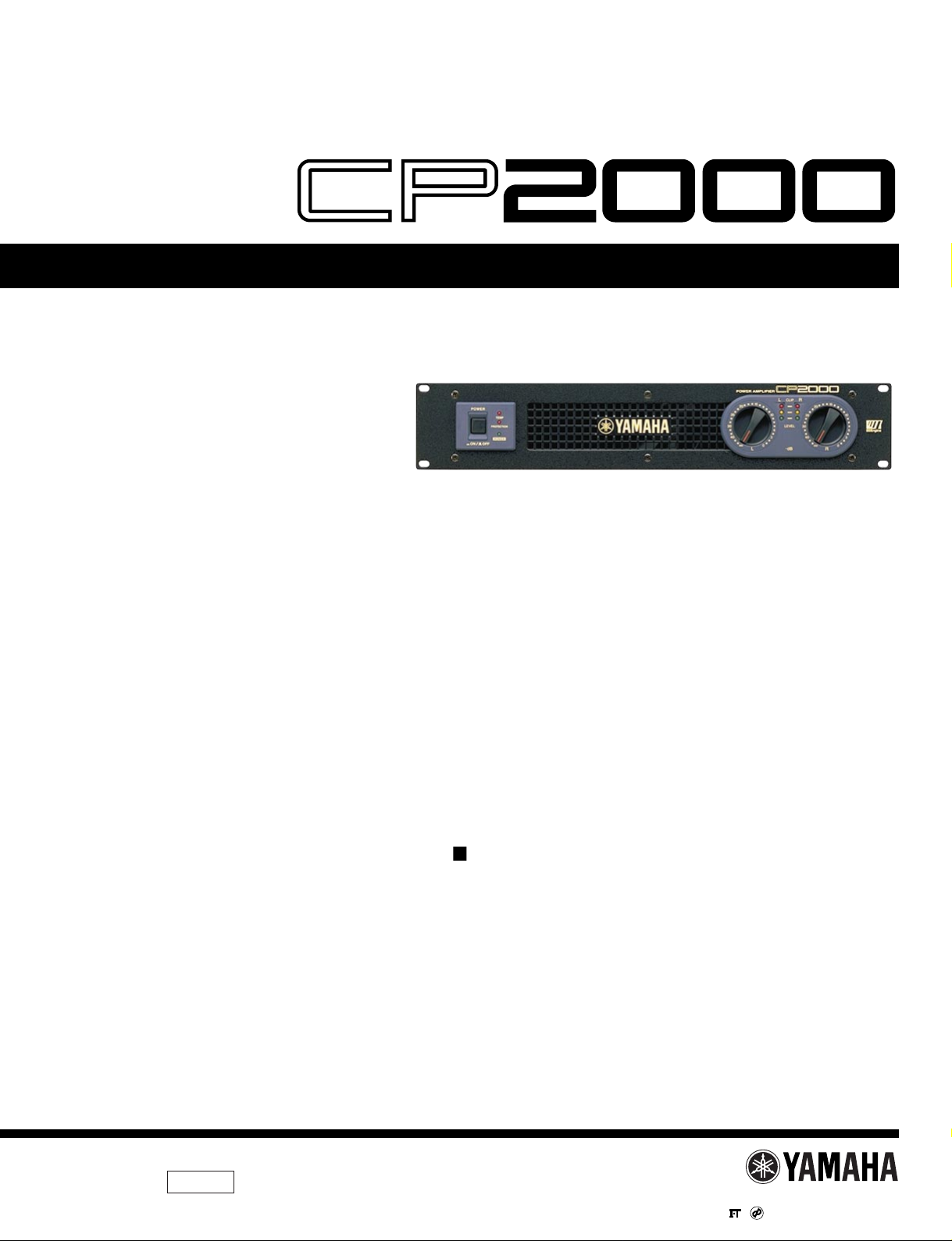
CP2000
2
WARNING: CHEMICAL CONTENT NOTICE!
The solder used in the production of this product contains LEAD. In addition, other electrical/electronic and/or plastic (where
applicable) components may also contain traces of chemicals found by the California Health and Welfare Agency (and possibly
other entities) to cause cancer and/or birth defects or other reproductive harm.
DO NOT PLACE SOLDER, ELECTRICAL/ELECTRONIC OR PLASTIC COMPONENTS IN YOUR MOUTH FOR ANY REASON
WHAT SO EVER!
Avoid prolonged, unprotected contact between solder and your skin! When soldering, do not inhale solder fumes or expose eyes
to solder/flux vapor!
If you come in contact with solder or components located inside the enclosure of this product, wash your hands before handling
food.
IMPORTANT NOTICE
This manual has been provided for the use of authorized Yamaha Retailers and their service personnel. It has been assumed that
basic service procedures inherent to the industry, and more specifically Yamaha Products, are already known and understood by
the users, and have therefore not been restated.
WARNING: Failure to follow appropriate service and safety procedures when servicing this product may result in personal
injury, destruction of expensive components and failure of the product to perform as specified. For these
reasons, we advise all Yamaha product owners that all service required should be performed by an authorized
Yamaha Retailer or the appointed service representative.
IMPORTANT: This presentation or sale of this manual to any individual or firm does not constitute authorization, certification,
recognition of any applicable technical capabilities, or establish a principal-agent relationship of any form.
The data provided is belived to be accurate and applicable to the unit(s) indicated on the cover. The research engineering, and
service departments of Yamaha are continually striving to improve Yamaha products. Modifications are, therefore, inevitable and
changes in specification are subject to change without notice or obligation to retrofit. Should any discrepancy appear to exist,
please contact the distributor's Service Division.
WARNING: Static discharges can destroy expensive components. Discharge any static electricity your body may have
accumulated by grounding yourself to the ground bus in the unit (heavy gauge black wires connect to this bus).
IMPORTANT: Turn the unit OFF during disassembly and parts replacement. Recheck all work before you apply power to the
unit.
WARNING
Components having special characteristics are marked and must be replaced with parts having specification equal to those
originally installed.
IMPORTANT NOTICE FOR THE UNITED KINGDOM
Connecting the Plug and Cord
IMPORTANT. The wires in this main lead are coloured in
accordance with the following code:
BLUE: NEUTRAL
BROWN: LIVE
As the colours of the wires in the main lead of this apparatus may not
correspond with the coloured markings identifying the terminals in
your plug, proceed as follows:
The BLUE wire must be connected to the terminal that is marked with
the letter N (or coloured BLACK).
The BROWN wire must be connected to the terminal that is marked
with the letter L (or coloured RED).
Be certain that neither core is connected to the earth terminal of the
three pin plug.
Page 3
SPECIFICATIONS
CP2000
3
Power Output Level 8 Ω/STEREO
1 kHz, THD+N=1 %
4 Ω/STEREO
8 Ω/BRIDGE
1 kHz 2 Ω/STEREO
20 ms, non-clip 4 Ω/BRIDGE
Power Bandwidth THD+N=0.2 % (half power)
Total Harmonic Distortion (THD+N) 4–8 Ω/STEREO
20 Hz–20 kHz (half power) 8 Ω/BRIDGE
Intermodulation Distortion 4–8 Ω/STEREO
60 Hz:7 kHz, 4:1, half power 8 Ω/BRIDGE
Frequency Response 8 Ω, Po=1W
Channel separation Half power, RL=8 Ω
LEVEL=max., input 600 Ω shunt
Residual Noise LEVEL=min., 12.7 kHz LPF, IHF-A network
S/N Ratio 12.7 kHz LPF
Damping Factor RL=8 Ω, 1 kHz
Sensitivity LEVEL=max., rated power into 8 Ω
Voltage Gain LEVEL=max.
Input Impedance
Front panel
Controls
Rear panel
Input
Connectors
Output
POWER
PROTECTION
TEMP
Indicators
CLIP
SIGNAL
Protection Circuit
Fan Circuit
Limiter Circuit
Power requirements
Idle Power Consumption
1/8 Power Consumption (4 Ω)
Maximum Power Consumption (4 Ω)
Dimensions (W x H x D)
Weight
AC Power cord length
450 W + 450 W
650 W + 650 W
1300 W
1000 W + 1000 W
2000 W
10 Hz—40 kHz
0.1%
0.1%
0 dB, +0.5 dB, -1 dB f=20 Hz—50 kHz
≥70 dB, 1 kHz
≤ -70 dB
104 dB
≥200
+4 dB
33.8 dB
30 kΩ (balanced), 15 kΩ (unbalanced)
POWER switch (push on/push off)
LEVEL attenuator (31 position) x2
Mode switch (STEREO/BRIDGE/PARALLEL)
YAMAHA SPEAKER PROCESSING switch (ON/OFF)
XLR-3-31 type (balanced) L+R
1/4" phone jack (balanced) L+R
1/4" phone jack L+R
5-way binding post x1
x1 (green)
x1 (red)
x1 (red) heatsink temp ≥85 °C
x2 (red)
x2 (green) output voltage ≥2 V
x2 (yellow) output voltage ≥20 V
POWER switch on/off mute
DC detection
TEMP (heatsink temp ≥90 °C)
PC limiter: RL ≤1 Ω
Stop–low speed (50 °C)–variable–high Speed (70 °C)
Comp: THD≥0.5 %
U.S.A. & Canada 120 V AC, 60 Hz
Europe 230 V AC, 50 Hz
Australia 240 V AC, 50 Hz
30 W
400 W
2000 W
480 x 88 x 416 mm (18.9 x 3.46 x 16.4 inches)
14 kg (30.9 lbs)
2.3 m
* 0 dB=0.775 V rms, half power = 1/2 output level.
Page 4
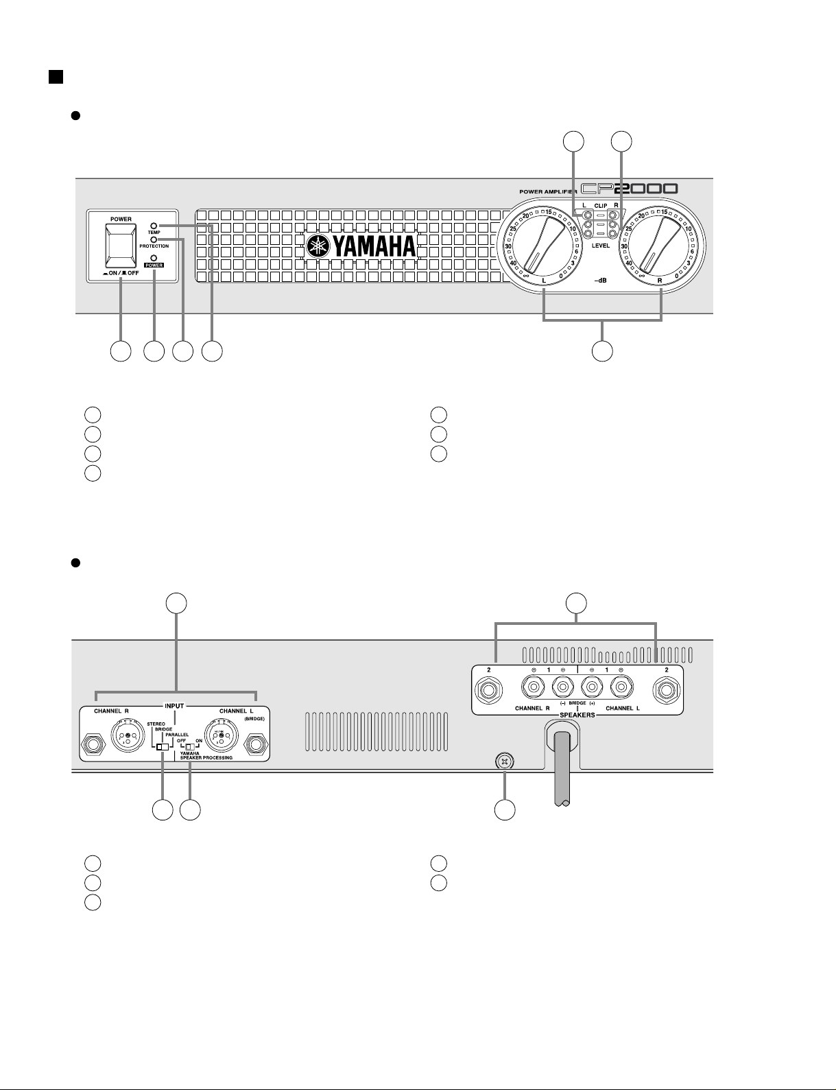
1
8
9 10 12
11
2 3 4 5
6 7
1
POWER switch
2
POWER indicator
3
PROTECTION indicator
4
TEMP indicator
5
Level controls
6
CLIP indicators
7
LEVEL indicators
8
INPUTs
9
Mode switch
10
YAMAHA SPEAKER PROCESSING switch
11
SPEAKERS connectors
12
GND terminal
CP2000
4
PANEL LAYOUT
Front Panel
Rear Panel
Page 5
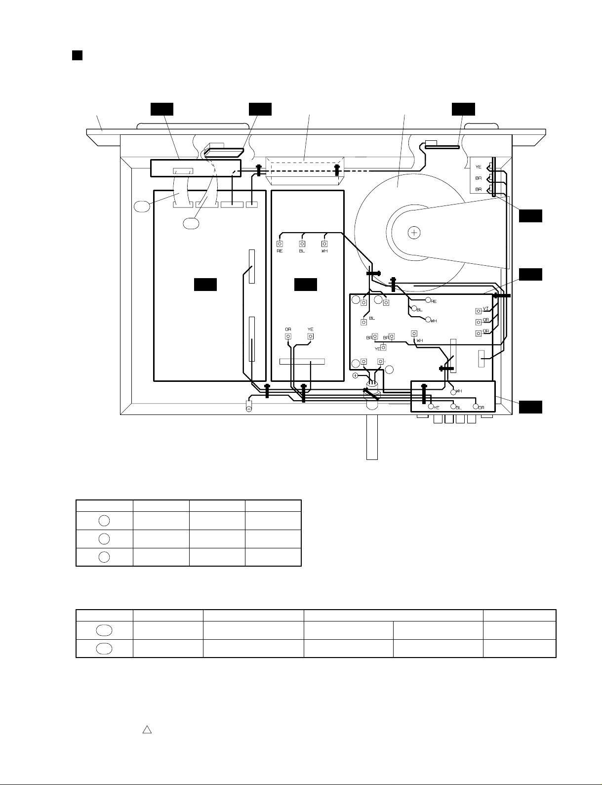
CIRCUIT BOARD LAYOUT
CP2000
5
70
80
CN615
CN303 CN305 CN304 CN302
CN616
CN606
CN607
CN608
CN612
CN610
CN609
CN611
CN614
CN313
CN603
CN604
CN605
CN601 CN602
CN301
CN102
CN105
CN106
CN101
CN103
CN104
CN306
CN617
AC 4/6
IN PA
AC 6/6 AC 5/6
AC 1/6
AC 2/6
AC 3/6
Power transformerFront panel Fan
AC 4/6-CN615 IN-CN303 7P 100mm
Connector AssemblyPart No.
MF107100
Location Destination Remarks
AC 6/6-CN617 IN-CN305 9P 120mmMF109120
70
80
3NC2-V617020
1 1
2
3
U, V, T H, W, B A
BR
WH
BL
BE
BE
BR
RE
BE
BR
• Wire Colors
1
2
3
2
Page 6

to Rear panel
AC cord
AC 4/6
IN
PA
AC 6/6
AC 5/6
AC 1/6
AC 2/6
AC 3/6
FAN
KEC-92573
POWER
TRANSFORMER
POWER
switch
3
CP2000
6
WIRING
Page 7
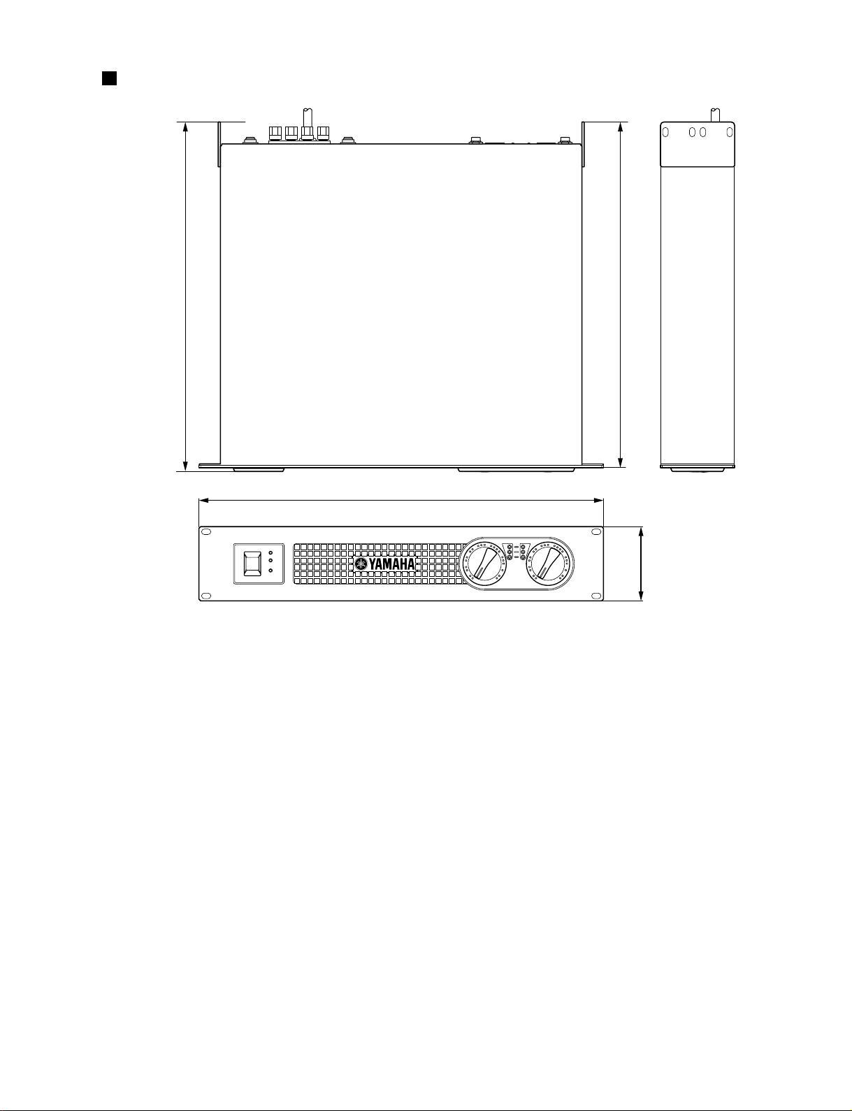
DIMENTIONS
CP2000
7
88
480
410
416
Unit: mm
Page 8
KEC-92572
1
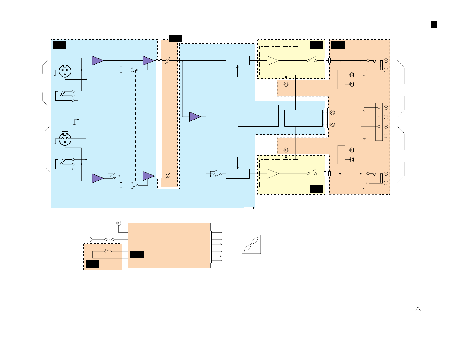
CHANNEL L
(BRIDGE)
(PARALLEL)
CHANNEL R
INPUT
JK301
JK303
12
3
2
3
1
JK302
JK304
12
3
2
5
7
6
+
-
3
1
BA
IC301
POWER
LD602
POWER CIRCUIT
AC Cord
POWER SW
SW601
3
1
2
+
-
BA
IC301
1
3
SW302
IC302
1
3
IC303
VR602
VR601
SW301
ON
OFF
CHANNEL
L
ATT
YAMAHA
SPEAKER
PROCESSING
SW302
ON
OFF
INV
CLIP
LD604
LD605
LD606
JK601
SP601
JK602
LD608
LD609
LD601
SIGNAL
SIGNAL
LD603
CLIP
LD607
CHANNEL
R
ATT
PARALLEL
BRIDGE
STEREO
Limiter
Lch Power Amp
Limiter
AC 4/6
AC 3/6, 5/6, 6/6
AC 1/6
AC 2/6,
CN615
IC302
76
CN303
IN
CN302
CN614
+B
E
-B
+24
E
-24
Rch Power Amp
Temperature
Sensor
(Heat Sink)
Protection
Circuit
CN304
CN616
PROTECTION
TEMP
PA
PA
W607
CN105
RY101
W609
CN106
RY102
SPEAKERS
CHANNEL L
L+R BRIDGE
CHANNEL R
FAN
Power transformer
8
CP2000
BLOCK DIAGRAM
Page 9
(Fig. 1)
(Fig. 2)
(Fig. 3) (Fig. 4)
[420]
[420] [420]
[420]
[420]: Bind Head Tapping Screw-B 4.0X8 MFZN2BL (EG340190)
[290]: Bonding Tapping Screw-B 3.0X8 MFZN2BL (VN413300)
[300]: Bind Head Tapping Screw-B 3.0X12 MFZN2BL (VQ074600)
[320]: Bind Head Tapping Screw-B 3.0X8 MFZN2BL (EP600190)
[103]: Bind Head Tapping Screw-B 4.0X8 MFZN2BL (EG340190)
[140]: Bind Head Tapping Screw-B 3.0X8 MFZN2BL (EP600190)
[80A]: Bind Head Screw A4.0X8 MFZN2BL (VP156800)
[120]: Bind Head Tapping Screw-B 3.0X8 MFZN2BL (EP600190)
[160]: Bonding Tapping Screw-B 4.0X8 MFZN2BL (VR779900)
[180]: Bind Head Tapping Screw-B 3.0X8 MFZN2BL (EP600190)
Top cover
<Top view>
<Rear view> <Side view>
[180][160]
IN
AC 3/6
AC 2/6
[290A] [320] [300] [320]
[A] [B]
[290B]
Speaker terminal cover
[B]
AC 3/6
[80A]
[120]
DB angle
DB angle
[140][103]
[C]
Transformer holder PA unitPower transformer
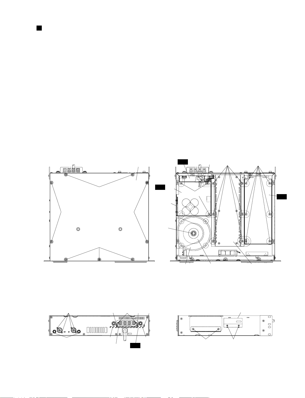
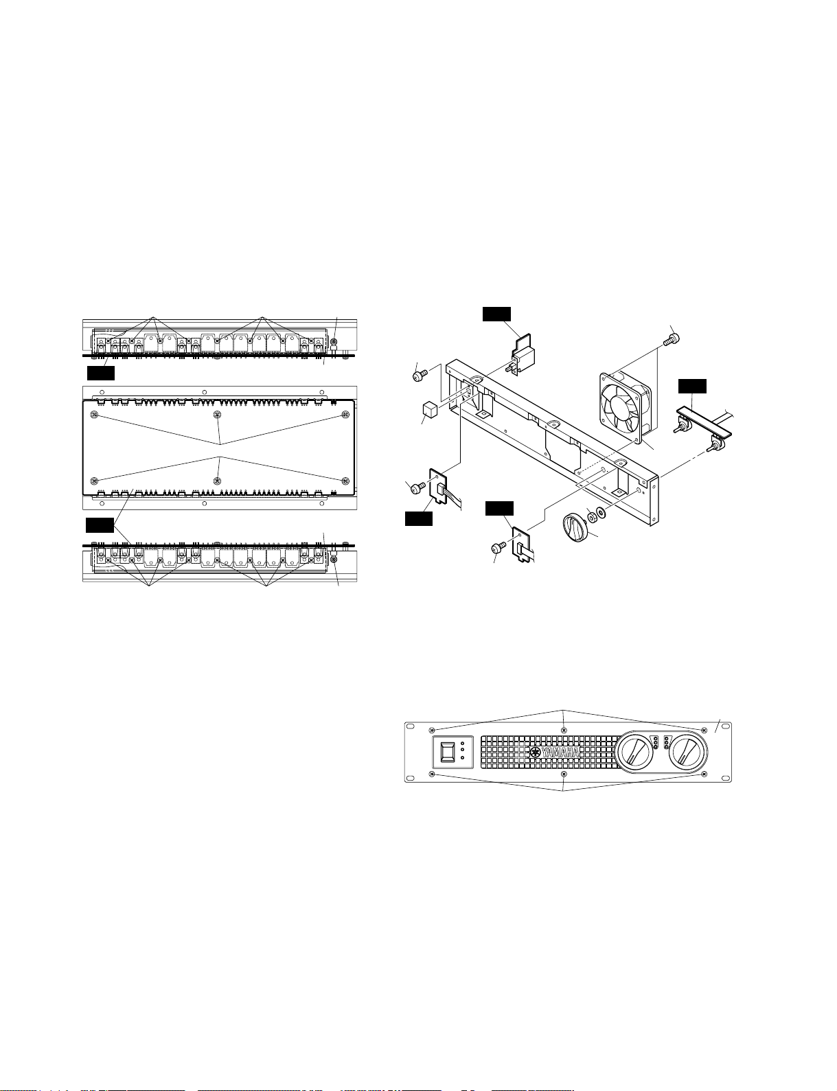
DISASSEMBLY PROCEDURE
CP2000
9
1. Top Cover(time required: about 3 minutes)
1-1 Remove the nine (9) screws marked [420]. The top cover
can then be removed. (Fig. 1)
2. IN Circuit Board(time required: about 8 minutes)
2-1 Remove the top cover. (See procedure 1.)
2-2 Remove the six (6) screws marked [180], the four (4) screws
marked [290A] and the two (2) hexagonal nuts marked [A].
The IN circuit board can then be removed. (Fig. 2, Fig. 3)
3. AC3/6 Circuit Board
(time required: about 10 minutes)
3-1 Remove the top cover. (See procedure 1.)
3-2 Remove the two (2) screws marked [320]. The speaker
terminal cover can then be removed. (Fig. 3)
3-3 Remove the screw marked [290B], the two (2) screws
marked [300] and the two (2) hexagonal nuts marked [B].
The AC3/6 circuit board can then be removed. (Fig. 3)
4. AC2/6 Circuit Board
(time required: about 15 minutes)
4-1 Remove the top cover. (See procedure 1.)
4-2 Remove the AC3/6 circuit board. (See procedure 3.)
4-3 Remove the screw marked [80A], the three (3) screws
marked [120] and the two (2) screws marked [140]. The
AC2/6 circuit board and the DB angle can then be removed.
(Fig. 2, Fig. 4)
5. Power Transformer
(time required: about 8 minutes)
5-1 Remove the top cover. (See procedure 1.)
5-2 Remove the two (2) screws marked [103] and the
hexagonal bolt marked [C]. The transformer holder and
the power transformer can then be removed. (Fig. 2, Fig. 4)
Page 10
[250]
(Fig. 7)
[250]
Front panel
<Front View>
[250]: Oval Head Screw 4.0X8 MFZN2BL (VS153600)
8. Front Panel (time required: about 5 minutes)
8-1 Remove the top cover. (See procedure 1.)
8-2 Remove the six (6) screws marked [250]. The front panel
can then be removed. (Fig. 7)
9.
AC1/6, A C4/6, AC5/6 and AC6/6 Cir cuit Boar d
(time required: about 20 minutes)
9-1 Remove the top cover. (See procedure 1.)
9-2 Remove the front panel (See procedure 8.)
9-3 AC1/6 Circuit Board:
Pull out the power switch knob. (Fig. 6)
Remove the two (2) screws marked [60]. The AC1/6 circuit
board can then be removed. (Fig. 6)
9-4 AC4/6 Circuit Board:
Pull out the attenuation knobs. (Fig. 6)
Remove the two (2) hexagonal nuts marked [D]. The AC4/6
circuit board can then be removed. (Fig. 6)
9-5 AC5/6 Circuit Board:
Remove the screw marked [100A]. The AC5/6 circuit board
can then be removed. (Fig. 6)
9-6 AC6/6 Circuit Board:
Remove the screw marked [100B]. The AC6/6 circuit board
can then be removed. (Fig. 6)
• PA Unit
[80B]
[80B]
[80B]
[80B]
[80B]
[80B]
(Fig. 5)
Transistor holder (L)
Transistor holder (R)
[40]
PA
PA
[40]: Bind Head Screw SP 3.0X8 MFZN2BL (EG330290)
[80B]: Bind Head Tapping Screw-B 3.0X12 MFZN2BL (VQ074600)
(Fig. 6)
[50]: Bind Head Screw 4.0X8 MFZN2BL (EG340360)
[60]: Bind Head Screw 3.0X8 MFZN2BL (VB659000)
[100]: Bind Head Tapping Screw-B 3.0X8 MFZN2BL (EP600190)
[60] x 2
[D]
[50]
Fan
AC 1/6
AC 4/6
Power switch
knob
Attenuation knob
AC 5/6
AC 6/6
[100A]
[100B]
CP2000
10
6. PA Unit & PA Circuit Board
(time required: about 15 minutes)
6-1 Remove the top cover. (See procedure 1.)
6-2 Remove the six (6) screws marked [160]. The PA unit can
then be removed. (Fig. 2)
6-3 Remove the eighteen (18) screws marked [80B]. And then
remove the left and right transistor holders from the PA unit.
(Fig. 5)
6-4 Remove the six (6) screws marked [40]. And then remove
the PA circuit board from the PA unit. (Fig. 5)
7. DC Fan (time required: about 8 minutes)
7-1 Remove the top cover. (See procedure 1.)
7-2 Remove the PA unit. (See procedure 6-2.)
7-3 Remove the two (2) screws marked [50]. The fan can then
be removed. (Fig. 6)
Page 11

IC BLOCK DIAGRAM
CP2000
11
M5238AP (XM085A00)
Dual Operational Amplifier
IN: IC301
NJM2068L-D (XM356A00)
Dual Operational Amplifier
IN: IC302, 303
1
2
3
4-V
8
7
6
5
Output A +V
Non-Inverting
Input A
-DC Voltage Supply
+DC Voltage
Supply
Output B
Inverting
Input B
Non-Inverting
Input B
Inverting
Input A
+-
+-
1A2 3 4 5 6 7 8
OUTA-INA+INA+INB-INBOUT
B
-V +V
-
+
B
-
+
CIRCUIT BOARDS CONTENTS
AC 1/6 Circuit Board (XY969B0)················································································ 12
AC 2/6 Circuit Board (XY969B0)················································································ 16
AC 3/6 Circuit Board (XY969B0)················································································ 13
AC 4/6 Circuit Board (XY969B0)················································································ 12
AC 5/6 Circuit Board (XY969B0)················································································ 12
AC 6/6 Circuit Board (XY969B0)················································································ 12
IN Circuit Board (XY968B0) ······················································································· 12
PA Circuit Board (XY970B0)······················································································ 14
Note: See parts list for details of circuit board component parts.
Page 12

to IN-CN303
Component side
LEVEL CONTROL L LEVEL CONTROL R
to IN-CN304
to IN-CN305
Component side
Component side
Component side
POWER ON/OFF
to AC 2/6-
CN601
to AC 2/6-
CN603
to AC 2/6-
CN602
POWER
PROTECTION
TEMP
LEVEL L
LEVEL R
CLIP L
CLIP R
A
A'
to FAN
to AC6/6
-CN617
to AC 5/6
-CN616
to AC 4/6
-CN615
to AC 2/6-CN614
CP2000
12
CIRCUIT BOARDS
IN: 3NA-V607200
AC 1/6, 4/6, 5/6, 6/6: 3NA-V607220
1
2
IN Circuit Board
AC 4/6 Circuit BoardAC 1/6 Circuit Board
AC 5/6 Circuit Board
AC 6/6 Circuit Board
Page 13

INPUT
CHANNEL R
CHANNEL L
YAMAHA
SPEAKER
PROCESSING
PARALLEL
BRIDGE
STEREO
(BRIDGE)
ON
OFF
A
A'
to PA-CN101
Component side
CP2000
13
Component side
SPEAKERS
(-) BRIDGE (+)
12 21
CHANNEL L CHANNEL R
to PA-CN106
to AC 2/6-CN612to PA-CN105
to REAR PANEL
IN: 3NA-V607200
AC 3/6: 3NA-V607220
1
2
AC 3/6 Circuit Board
Page 14

CP2000
14
B
B'
CN101:
CN102:
to IN-CN306
to AC 2/6-W604
CN103:
CN104:
to AC 2/6-W605
to AC 2/6-W606
CN105:
CN106:
to AC 3/6-W607
to AC 3/6-W609
PA Circuit Board
3NA-V60721
1
Page 15

CP2000
15
B
B'
Component side
3NA-V60721
1
Page 16

Component side
CN601:
CN602:
CN603:
CN604:
CN605:
to AC 1/6-W601
to AC 1/6-W602
to AC 1/6-W603
to AC cord (L)
to AC cord (N)
CN606:
CN607:
CN608:
CN609:
CN610:
to Power transformer
to Power transformer
to Power transformer
to Power transformer
to Power transformer
CN611:
CN612:
W604:
W605:
W606:
to Power transformer
to AC 3/6-W608
to PA-CN102
to PA-CN103
to PA-CN104
to IN-CN301
to Power
transformer
U, V, T
H, W, B
A
BL
CN604
BR
BR
WH
CN605
BE
BE
BR
CN606, CN607
BE
RE
• Wire Colors
CP2000
16
AC 2/6 Circuit Board
3NA-V607220
2
Page 17

INSPECTIONS
CP2000
17
1. Inspection during stereo mode and parallel mode
1.1 Preparations
1.2 Inspection and adjustment
1.2.1 Fan and temperature indicator
The fan shall operate when the two jumper wires inside the frame marked
FAN-C inside sheet IN are shorted. Next, the temperature indicator shall
come on when the two jumper wires inside the frame marked TM-C are
shorted. (Refer to the figure to the right for FAN-C, TM-C.)
1.2.2 Power on muting time
At t=2.5 ± 1 seconds after the power switch is turned on, the muting shall be cancelled and the protection indicator shall go off.
1.2.3 Idling current
Ground the input terminal and adjust VR101 (L ch) and VR102 (R ch) so that the CN108 (L ch) and CN107 (R ch) No. 1 and 2
terminals show DC voltage of Vb=0.5 ± 0.1 mV.
Once all inspections have been completed, re-inspect Vb and adjust so that it is Vb=0.5 ± 0.1 mV.
1.2.4 Output terminal DC voltage
Ground the input terminal and measure the Vdc (direct current voltage) of the output terminal. It shall be Vdc=0 ± 75 mV.
1.2.5 Gain
An output voltage of +24.0 ± 0.5 dBu shall be attained when 1 kHz, -10.0 dBu sine wave is input to the input terminal.
This inspection shall also be performed in the PARALLEL mode.
1.2.6 Frequency characteristics
* YAMAHA SPEAKER PROCESSING OFF:
Using 1 kHz as a standard for the output voltage, the output voltage shall be within -0.5 ± 0.5 dB at 20 kHz when 20 Hz, 1 kHz,
20 kHz, -10 B dBu sine waves are input to the input terminal.
* YAMAHA SPEAKER PROCESSING ON:
Using 1 kHz as a standard for the output voltage, with the Yamaha speaker processing off, the output voltage shall be within +
6.5 ±1.5 dB when a 70 Hz, -10 dBu sine wave is input to the input terminal.
1.2.7 Total harmonic distortion ratio characteristics
The total harmonic distortion ration shall be THD=1 % or less when a 1 kHz high definition sine wave is input to the input terminal
and the rated output of 650 w + 650 w / 4 ohm (36.4 dBu/ch) has been attained. This inspection shall be completed within 30 seconds.
1.2.8 Channel separation load resistance 8 Ω
When the input terminal for one of the channels has attained a 1kHz, -5dBu sine wave has and that input terminal is grounded by
the introduction of 600 Ω resistance, the measured output voltage of the other channel shall by -70 dB or less, using a output voltage
with (0 dB) as the reference level.
1.2.9 Output noise level
Measure the noise level at the output terminal when the input attenuator has been set to MAX and a input terminal has been grounded
by the introduction of a 600 Ω resistance. It shall be -67 dBu or less. Next, set the input attenuator to MIN and measure. It shall be
-70 dBu or less.
Input attenuator
Input terminal
Mode SW
Yamaha speaker processing
Output terminal
Others
MAX
Cannon connector No. 2 hot; No. 1, 3 ground
Stereo
Off
Resistance load 4 Ω, Non inductance resistor, input capacitance 500 W or more.
Unless otherwise specified, drive both channels unless otherwise specified.
INPA
AC 3/6
AC 2/6
TM-C
FAN-C
<Top View>
Page 18

1.2.10 Stability
The following conditions shall be met when a 10 kHz, -10dBu rectangular pulse is input and a capacitance of 10 pf ~ 0.47 µF is
connected in parallel with a load resistance of 4 Ω.
Overshoot Vp/Vo 1.8
Ringing: Within 5 waves
Next, when there is only a pure capacitance of 10 pf ~ 0.47 µF the following conditions shall be met.
Vp/Vo 2.5
Ringing: There shall be convergence within 7 waves and no oscillation, etc.
1.2.11 Protection circuit
The protection circuit shall operate and the relay shall not open when a 10 Hz, +5.4 dBu sine wave is input and the output wave is
made to clip. Next, the protection circuit shall operate within two seconds and break the output when a 1 Hz, 0.0 dBu sine wave is
input. In addition, when the input signal is cut, it shall automatically recover within 10 seconds.
1.2.12 Efficiency
(1) The primary electrical power shall be measured and be within the range shown below when a 1 kHz, -6.6 dBu sine wave is input
to the input terminal.
330 W ± 50 W (U: 4.0 A ± 0.6 A, H: 2.0 A ± 0.3A)
(2) The primary electrical power shall be measured and be within the range shown below when the input terminal is grounded by the
introduction of the input terminal.
25 W ± 10 W (U: 0.33 A ± 0.13 A, H: 0.20 A ± 0.08 A)
1.2.13 PC limiter and comp
Input a 1 kHz, -1.5 dBu sine wave to the input terminal and connect 1 Ω (± 5 %) as a load to the output terminal. Under these conditions,
a 10 V Vrms 16 V sine wave shall be attained at the output. The total harmonic distortion ratio shall be THD=5 % or less.
Also at this time, the clip indicator shall come on. This inspection shall be completed within 30 seconds.
1.2.14 Signal indicator
The green signal indicator shall come on when a 1 kHz, -23 dBu sine wave is input.
In addition, the green and yellow signal indicators shall come on when a 1 kHz, -4 dBu sine wave is input.
2. Bridge mode
2.1 Preparations
2.2 Inspection
2.2.1 Gain
An output voltage of +24.0 ± 1.0 dBu shall be attained when a 1 kHz, -10 dBu sine wave is input to the input terminal.
<
=
<
=
<
=
<
=
CP2000
18
Input attenuator
Input terminal
Mode SW
Yamaha speaker processing
Output terminal
Load resistance
Measurement connection
L channel only operates. Set to MAX.
L channel cannon connector (No. 2 hot, No. 1, 3 ground)
Bridge
Off
Use L channel +, R channel +.
4 Ω + 4Ω, Non inductance resistor, input capacitance 500 W or more.
Set to a floating ground and connect at center point of load resistance.
SPEAKERS
INPUT
MEASURING
INSTRUMENT
GND
Page 19

CP2000
19
2.2.2 Frequency characteristics
Using 1 kHz as a standard for the output voltage, the output voltage shall be within -0.5 ± 0.5 dB at 20 kHz when 20 Hz, 1 kHz, 20
kHz, -10 B dBu sine waves are input to the input terminal.
2.2.3 Total harmonic distortion ratio characteristics
The total harmonic distortion ration shall be 1 % or less when a 1 kHz high definition sine wave is input to the input terminal and the
output voltage of 36.4 dBu has been attained. This inspection shall be completed within 30 seconds.
2.2.4 Output noise level
Measure the noise level at both terminals of the load resistance when the input attenuator has been set to MAX and the input
terminal has been grounded by the introduction of a 600 Ω resistance. It shall be -60 dBu or less. Next, set the input attenuator to
MIN and measure. It shall be -60 dBu or less.
3. Process after completion of inspection
Close up the input attenuator in a half-clockwise direction.
Set YAMAHA SPEAKER PROCESSING to on.
Set the mode switch to STEREO.
4. Others
A DIN audio filter shall be used for the measurement of the noise level.
0 dBu=0.775 V
Page 20

CONTENTS
OVERALL ASSEMBLY······························································································································ 2
ELECTRICAL PARTS ·························································································································5~12
PARTS LIST
WARNING
Components having special characteristics are marked and must be replaced with parts having
specification equal to those originally installed.
A: Australian model
B: British model
C: Canadian model
D: German model
E: European model
F: French model
H: North European model
I : Indonesian model
J: Japanese model
M: South African model
O: Chinese model
Q: South-east Asia model
T: Taiwan model
U: U.S.A. model
V: General export model (110 V)
W: General export model (220 V)
N,X:General export model
Y: Export model
Notes: DESTINATION ABBREVIATIONS
• The numbers in “ QTY ” show quantities for each unit.
• The parts with “ - - ” in “ PART NO. ” are not available as spare parts.
• The mark “ ” in the remarks column indicates that these parts are interchangeable.
• The second letter of the shaded ( ) part number is O, not zero.
• The second letter of the shaded ( ) part number is I, not one.
POWER AMPLIFIER
Page 21

420
400
40 40a
70
50
60
330
300
310
320
360
290
280
190
Front Sub
Assembly
120
F70
F50
F10
P80
P40
P30
P80
P80
P20
P10
P70
P50
150
PA Unit
P60
F60
F90
F80
F110
F100
F100
F120
F20
330
360
390
430
111
112
10
130
350
340
140
210
220
230
270
260
250
240
113
160
180
170
80
100
101
95
97
96
145
102
103
90
20
30
370
380
200
290
410
110f
110e
110a
110d
110b
110c
340
350
CP2000
2
OVERALL ASSEMBLY
Page 22

CP2000
3
OVERALL ASSEMBLY
Overall Assembly
Overall Assembly
Overall Assembly
Overall Assembly
Overall Assembly
Main Chassis
Main Chassis
Protection Sheet
Protection Sheet
AC Cord
AC Cord
AC Cord
AC Cord Assembly
AC Cord
Cord Strain Relief
Bushing
Ferrite Core
Cord Holder
Bind Head Screw
Label
Shield sheet
Shield sheet
Shield sheet
Power Transformer
Power Transformer
Power Transformer
Holder, Transformer
Bushing
Bind Head Tapping Screw-B
Circuit Board
Circuit Board
Circuit Board
Circuit Board
Circuit Board
Circuit Board
Circuit Board
Circuit Board
Circuit Board
Circuit Board
Circuit Board
Vibration-proof Rubber
Vibration-proof Rubber
Vibration-proof Rubber
Bind Head Tapping Screw-B
DB Angle
Bind Head Tapping Screw-B
Shield sheet
PA Unit
Bonding Tapping Screw-B
Circuit Board
Bind Head Tapping Screw-B
Front Sub Assembly
Bind Head Tapping Screw-B
Bonding Tapping Screw-B
Front Grille
Bind Head Tapping Screw-B
Front Panel
Oval Head Screw
Escutcheon, ATT
Escutcheon, PSW
Rear Panel
Rear Panel
Rear Panel
Rear Panel
Bonding Tapping Screw-B
Bind Head Tapping Screw-B
Cover, Speaker Terminal
Bind Head Tapping Screw-B
Bonding Tapping Screw-B
DESCRIPTION
10
10
20
30
40
40
40
40
40a
50
50
60
70
80
90
95
96
97
100
100
100
101
102
103
110
110
110
110a
110b
110b
110b
110c
110d
110e
110f
111
112
113
120
130
140
145
150
160
170
180
190
200
210
220
230
240
250
260
270
280
280
280
280
290
300
310
320
330
REF NO.
- -
- -
- -
- -
- V6170900
V6308400
V6171000
V6171100
VZ021200
V2944000
VZ021600
- VD280500
VV103100
VB669000
V3225000
VV104600
VP156800
- -
- -
- -
- XY980A00
XY981A00
XZ157A00
V6305500
V6305600
EG340190
- -
- -
- AAX20810
AAX20820
AAX20830
AAX20840
AAX20850
AAX20860
AAX20870
AAX20880
V6511200
V6511300
V6800300
EP600190
- EP600190
- V6170800
VR779900
V6072000
EP600190
- EG340190
VR779900
V6171300
EP600190
V6171400
VS153600
V6171500
V6171600
V6171700
V6171800
V6171900
V6172000
VN413300
VQ074600
VY938700
EP600190
VR779900
PART NO.
A PPE T=0.3
B PPE T=0.3
SJT 3X#18 10A
H05VV-F0.75X3 6A
H05VV-F 13A
U 3P 15A 2.5m
SR-6P1
SR-7P-2
FR25/15/12-D40
A4.0X8 MFZN2BL
GND
A
B
C
UL E
CE E
A E
TKK
4.0X8 MFZN2BL
AC U
AC H
AC A
AC 1/6
AC U 2/6
AC H 2/6
AC A 2/6
AC 3/6
AC 4/6
AC 5/6
AC 6/6
A
B
C
3.0X8 MFZN2BL
3.0X8 MFZN2BL
D
4.0X8 MFZN2BL
IN
3.0X8 MFZN2BL
4.0X8 MFZN2BL
4.0X8 MFZN2BL
3.0X8 MFZN2BL
4.0X8 MFZN2BL
3.0X8 MFZN2BL
3.0X12 MFZN2BL
P-SERIES
3.0X8 MFZN2BL
4.0X8 MFZN2BL
CP2000
U,V (V617020)
H,W (V617030)
B (V617040)
A (V617050)
T (V617060)
U,V,H,W,B,A
T
U,V
H,W,A
B
T (V245650)
T
U,V,H,W,B,A
T
H,W,B
H,W,B
H,W,B (V542870)
H,W,B (V701980)
H,W,B (V701990)
H,W,B (V702000)
U,V,T
H,W,B
A
U,V,T (V607220)
H,W,B (V607230)
A (V688310)
U,V,T
H,W,B
A
(V617120)
H,W,B (V702010)
(V617410)
U,V
H,W,B
A
T
REMARKS
2
2
2
3
2
6
6
2
4
3
6
5
2
2
6
QTY
RANK
*
*
*
*
*
*
*
*
*
*
*
*
*
*
*
*
*
*
*
*
*
*
*
*
*
*
*
*
*
*
06
06
08
08
01
02
03
01
01
01
01
01
01
01
01
01
01
01
01
01
03
01
01
*
:
New Parts RANK: Japan only
Page 23

CP2000
4
Rear Angle
Bind Head Tapping Screw-B
Bind Head Screw
Connector Assembly
Connector Assembly
Cord Holder
Top Cover
Cover
Bind Head Tapping Screw-B
Label
PA Unit
Heat Sink
Support
Circuit Board
Bind Head Screw
Insulation Sheet
Transistor Holder
Transistor Holder
Bind Head Tapping Screw-B
Front Sub Assembly
Front Chassis
Fan
Bind Head Screw
Bind Head Screw
Connector Assembly
Connector Assembly
Connector Assembly
Bind Head Tapping Screw-B
Power Switch Knob
Attenuation Knob
DESCRIPTION
340
350
360
370
380
390
400
410
420
430
P10
P20
P30
P40
P50
P60
P70
P80
F10
F20
F50
F60
F70
F80
F90
F100
F110
F120
REF NO.
VY937100
EG340190
VP156800
- -
- VV104600
VY937600
V6172200
EG340190
VA039300
V6170800
- VV086500
V6072100
EG330290
V6172500
V6172600
V6172700
VQ074600
- -
- V6622900
EG340360
VB659000
MF107100
MF109120
V6186100
EP600190
VU859000
VY938500
PART NO.
P-SERIES
4.0X8 MFZN2BL
A4.0X8 MFZN2BL
PA 15P
AC-IN 8P
P-SERIES
PPE T=0.3
4.0X8 MFZN2BL
H=7.4 B=5.5
PA
SP 3.0X8 MFZN2Y
TBM51W T=0.15
LEFT
RIGHT
3.0X12 MFZN2BL
KDE2408PTS1-6A-318
4.0X8 MFZN2BL
3.0X8 MFZN2BL
7P 100mm P=1.25
9P 120mm P=1.25
IND 4P
3.0X8 MFZN2BL
P-SERIES
(V618590)
(V618600)
U,V
(V617230)
(V617410)
(V617280)
POWER
LEVEL CONTROL
REMARKS
2
4
2
9
2
9
6
6
2
18
2
2
2
2
QTY
RANK
*
*
*
*
*
*
*
*
*
*
03
01
01
01
10
01
03
01
01
01
01
01
01
01
03
*
:
New Parts RANK: Japan only
Page 24

CP2000
5
ELECTRICAL PARTS
Circuit Board
Circuit Board
Circuit Board
Circuit Board
Circuit Board
Circuit Board
Circuit Board
Circuit Board
Circuit Board
Circuit Board
Circuit Board
Circuit Board
Circuit Board
Circuit Board
Circuit Board
Circuit Board
Circuit Board
Circuit Board
Circuit Board
Circuit Board
Circuit Board
Circuit Board
Circuit Board
Circuit Board
Fuse Holder
LED Spacer
Jumper Wire
Mylar Capacitor
Mylar Capacitor
Capacitor
Capacitor
Mylar Capacitor
Mylar Capacitor
Capacitor
Electrolytic Cap.
Electrolytic Cap.
Capacitor
Electrolytic Cap.
Electrolytic Cap.
Electrolytic Cap.
Electrolytic Cap.
Electrolytic Cap.
Capacitor
Ceramic Capacitor-B
Ceramic Capacitor-B
Ceramic Capacitor-B
Ceramic Capacitor-B
Diode
Diode
Diode Stack
Diode
Fuse
Fuse
Fuse
Fuse
Fuse
Fuse
Fuse
Fuse
GND Plate
Terminal Plate
Flame Proof C. Resistor
Flame Proof C. Resistor
Carbon Resistor
Flame Proof C. Resistor
Flame Proof C. Resistor
Flame Proof C. Resistor
Flame Proof C. Resistor
DESCRIPTION
C601
C602
C603
C604
C605
C606
C607
C608
C609
C610
C611
C612
C613
C614
C615
C616
C617
-620
C621
-623
D601
-604
D605
D606
F601
F601
F602
F602
F603
F603
F604
F604
K601
K602
R601
R602
R603
R604
R605
R606
R607
REF NO.
- -
- -
- AAX20810
AAX20820
AAX20830
AAX20840
AAX20850
AAX20860
AAX20870
AAX20880
V6072000
V6072100
- -
- -
- AAX20810
AAX20820
AAX20830
AAX20840
AAX20850
AAX20860
AAX20870
AAX20880
VV319600
VV307300
- V3148500
V3148500
V6113500
V6185400
VZ004200
VZ004200
V6113500
V6183300
V6183300
V6185400
V6183300
V6183300
V5482000
V5482000
UR866470
VZ411400
VZ012200
VZ012200
VV314600
VV314600
VU801600
VU801600
V4833600
VU801600
KB001540
VT943200
KB001540
VT943200
VV070300
VV071200
VV070300
VV071200
VZ703700
VV075700
VV276700
VV276700
HF457150
VV276700
VV276700
VZ008800
VV276700
PART NO.
AC U
AC H
AC A
AC 1/6
AC U 2/6
AC H 2/6
AC A 2/6
AC 3/6
AC 4/6
AC 5/6
AC 6/6
IN
PA
AC U
AC H
AC A
AC 1/6
AC U 2/6
AC H 2/6
AC A 2/6
AC 3/6
AC 4/6
AC 5/6
AC 6/6
CQ-05CT
0.60
0.33 250V M
0.33 250V M
1000P 400V J.U.C.S
3300P 400V J.U.C.S
0.1000 100V M
0.1000 100V M
1000P 400V J.U.C.S
3300 160V
3300 160V
3300P 400V J.U.C.S
3300 160V
3300 160V
1000 35.0V
1000 35.0V
4.70 50.0V
0.22 275V UCS
0.001 500V K
0.001 500V K
0.0022 500V K
0.0022 500V K
1N4004L 26
1N4004L 26
RBV2506 25.0A 600V
1N4004L 26
12.00A UL
TH 5.00A S
12.00A UL
TH 5.00A S
TDS 1A 250V J/U/C
TSD 1A 250V SEMKO
TDS 1A 250V J/U/C
TSD 1A 250V SEMKO
P-SERIES
4.7 1/4 J
4.7 1/4 J
15.0K 1/4 J
4.7 1/4 J
4.7 1/4 J
22.0 1/4 J
4.7 1/4 J
CP2000
U,V,T (V607220)(XY969C0)
H,W,B (V607230)(XY969C0)
A (V688310)(XY969C0)
(XY969C0)
U,V,T (XY969C0)
H,W,B (XY969C0)
A (XY969C0)
(XY969C0)
(XY969C0)
(XY969C0)
(XY969C0)
(XY968B0)
(XY970B0)
U,V,T (V607220)(XY969B0)
H,W,B (V607230)(XY969B0)
A (V688310)(XY969B0)
(XY969B0)
U,V,T (XY969B0)
H,W,B (XY969B0)
A (XY969B0)
(XY969B0)
(XY969B0)
(XY969B0)
(XY969B0)
(VV29140)
U,V,T
H,W,B
U,V,T
H,W,B
U,V,T
H,W,B
U,V,T
H,W,B
REMARKS
8
9
QTY
RANK
*
*
*
*
*
*
*
*
*
*
*
*
*
*
*
*
*
*
*
*
*
*
*
*
*
01
01
01
01
01
01
01
01
01
01
01
01
01
01
04
01
04
01
04
01
01
01
01
01
01
01
01
01
01
01
01
01
01
ELECTRICAL PARTS
*
:
New Parts RANK: Japan only
Page 25

CP2000
6
Flame Proof C. Resistor
Relay
Connector Assembly
Connector Assembly
Connector Assembly
Connector Assembly
Connector Assembly
Connector Assembly
Connector Assembly
Connector Assembly
Connector Assembly
Connector Assembly
Fasten Terminal
Fasten Terminal
Base Post Connector
Connector Base Post
Connector, FFC
Connector Base Post
Connector, FFC
Base Post Connector
Phone Jack
Phone Jack
LED Red
LED Green
LED Red
LED Red
LED Yellow
LED Green
LED Red
LED Yellow
LED Green
Speaker Terminal
Push Switch
Rotary Variable Resistor
Rotary Variable Resistor
Circuit Board
Jumper Wire
Ceramic Capacitor-SL
Ceramic Capacitor-SL
Electrolytic Cap.
Ceramic Cap.-B
Ceramic Capacitor-SL
Ceramic Capacitor-SL
Electrolytic Cap.
Electrolytic Cap.
Ceramic Capacitor-SL
Ceramic Capacitor-SL
Ceramic Capacitor-SL
Electrolytic Cap.
Electrolytic Cap.
Electrolytic Cap.
Electrolytic Cap.
Ceramic Capacitor-F
Mylar Capacitor
Mylar Capacitor
Mylar Capacitor
Mylar Capacitor
Electrolytic Cap.
Electrolytic Cap.
Mylar Capacitor
Mylar Capacitor
Ceramic Capacitor-F
Mylar Capacitor
Mylar Capacitor
Ceramic Capacitor-B
Ceramic Capacitor-B
Electrolytic Cap.
Electrolytic Cap.
Ceramic Cap.-B
DESCRIPTION
R608
RY601
W601
W602
W603
W604
W605
W606
W607
W608
W609
W610
CN601
-612
CN613
CN614
CN615
CN616
CN617
CN618
JK601
JK602
LD601
LD602
LD603
LD604
LD605
LD606
LD607
LD608
LD609
SP601
SW601
VR601
VR602
C301
-304
C305
C306
C307
C308
C309
C310
C311
C312
C313
C314
C315
C316
C317
C318
C319
-322
C323
C324
C325
C326
C327
C328
C329
C330
C331
C332
C333
C334
C335
C336
REF NO.
VZ008800
VZ003600
V6186600
V6186600
V6186500
V6186300
V6186200
V6186400
V6185800
V6185500
V6185700
V6186700
VZ005700
VZ005700
LB932030
V3764600
VQ044300
V3765600
VQ044400
LB932020
VV089300
VV089300
VV620800
VV621000
VV620800
VV620800
VV938100
VV621000
VV620800
VV938100
VV621000
VZ956900
VY898100
VI575600
VI575600
V6072000
- VZ352800
VZ352800
UR866100
VZ353900
VZ353300
VZ353300
UR867100
UR867100
VZ353300
VZ353300
VZ352800
VV330700
UR847470
UR867100
UR867100
VZ354000
VV062900
VV062900
V5868900
V5868900
UR867100
UR866470
V5868900
V5868900
VZ354000
V5868900
V5868900
VV314600
VV314600
UR867100
UR867100
VZ353900
PART NO.
22.0 1/4 J
24V
SWR, BR
SWR, BR
SWY, YE
+B, RE
CENT, BL
-B, WH
L, OR
GND, WH
R, YE
EARTH, BL
TP82223-22
TP82223-22
VH- 3P TE
M24185XX 8P TE
52044 7P SE
M24185XXR 4P SE
52044 9P SE
VH- 2P TE
H30280072N
H30280072N
LT311G-41-C13
LT321-41-C13
LT311G-41-C13
LT311G-41-C13
LT331-41-C13
LT321-41-C13
LT311G-41-C13
LT331-41-C13
LT321-41-C13
STB-403AU 4P
SDDFA3107U-YL UCS
5K
5K
IN
0.60
22P 50V J
22P 50V J
1.00 50.0V
1000P 50V K
56P 50V J
56P 50V J
10.00 50.0V
10.00 50.0V
56P 50V J
56P 50V J
22P 50V J
470.00 10.0V
47.00 25.0V
10.00 50.0V
10.00 50.0V
0.0100 50V Z
0.12 50V J
0.12 50V J
0.1 50V J
0.1 50V J
10.00 50.0V
4.70 50.0V
0.1 50V J
0.1 50V J
0.0100 50V Z
0.1 50V J
0.1 50V J
0.0022 500V K
0.0022 500V K
10.00 50.0V
10.00 50.0V
1000P 50V K
H,W,B
SPEAKERS 2 LEFT
SPEAKERS 2 RIGHT
PROTECTION
POWER
TEMP
ACLP
ASIGH
ASIGL
BCLP
BSIGH
BSIGL
SPEAKERS 1
POWER ON/OFF
LEVEL CONTROL L
LEVEL CONTROL R
(XY968B0)
(VV29140)
REMARKS
QTY
RANK
*
*
*
*
*
*
*
*
*
*
*
*
*
01
01
01
01
01
01
01
02
02
01
01
01
01
01
01
01
01
01
06
05
03
03
01
01
01
01
01
01
01
01
01
01
01
01
01
01
01
01
01
01
01
01
01
01
01
01
01
01
01
*
:
New Parts RANK: Japan only
Page 26

CP2000
7
Electrolytic Cap.
Electrolytic Cap.
Electrolytic Cap.
Electrolytic Cap.
Electrolytic Cap.
Ceramic Capacitor-SL
Ceramic Capacitor-SL
Electrolytic Cap.
Electrolytic Cap.
Mica Capacitor
Mica Capacitor
Ceramic Cap.-B
Electrolytic Cap.
Electrolytic Cap.
Mylar Capacitor
Mylar Capacitor
Electrolytic Cap.
Electrolytic Cap.
Electrolytic Cap.
Connector Base Post
Connector Base Post
Connector, FFC
Connector Base Post
Connector, FFC
Connector Base Post
Zener Diode
Diode
Diode
Zener Diode
Diode
Diode
Diode
Zener Diode
Diode
Diode
Noise Filter
Noise Filter
IC
IC
IC
IC
IC
XLM Connector
XLM Connector
Phone Jack
Phone Jack
GND Plate
Photo Coupler
Photo Coupler
Transistor
Transistor
Transistor
Transistor
Transistor
Transistor
Transistor
Transistor
Transistor
Transistor
Transistor
Digital Transistor
Digital Transistor
Transistor
Digital Transistor
Transistor
Transistor
Transistor
Transistor
Digital Transistor
Digital Transistor
DESCRIPTION
C337
C338
C339
C340
C341
C342
C343
C344
C345
C346
C347
C348
C349
C350
C351
C352
C353
C354
C355
CN301
CN302
CN303
CN304
CN305
CN306
D301
D302
-307
D308
D309
D310
D311
D312
D313
-320
EM301
-304
IC301
IC302
IC303
IC304
IC305
JK301
JK302
JK303
JK304
K301
PH301
PH302
Q301
Q302
Q303
Q304
Q305
Q306
Q307
Q308
Q309
Q310
Q311
Q312
Q313
Q314
Q315
Q316
Q317
Q318
Q319
Q320
Q321
REF NO.
UR866100
V6638400
V6638400
UR866100
UR866100
FG652100
FG652100
UR828100
UR828100
FU451220
FU451220
VZ353900
UR866100
UR866100
VV060300
VV060300
UR847100
UR847100
UR866100
V3764600
V3764000
VQ047100
V3764200
VQ047200
V3765300
VG440800
VD631600
VD631600
VG440300
VU801600
VU801600
VD631600
VG437700
VD631600
VD631600
V3260500
V3260500
XM085A00
XM356A00
XM356A00
XD853A00
XD854A00
VS133800
VS133800
VY898300
VY898300
VZ703700
VP116000
VP116000
V2797600
V2797700
V2797600
V2797700
V2797700
V2797600
V2797700
V2797600
V2797600
VS883300
V2797700
VD678500
VD678500
V2797700
VD678500
V2797600
V2797600
V2797700
V2797700
VD678500
VD678500
PART NO.
1.00 50.0V
22.00 25.0V
22.00 25.0V
1.00 50.0V
1.00 50.0V
100P 50V J
100P 50V J
100.00 10.0V
100.00 10.0V
22P 500V J
22P 500V J
1000P 50V K
1.00 50.0V
1.00 50.0V
2200P 50V J
2200P 50V J
10.00 25.0V
10.00 25.0V
1.00 50.0V
M24185XX 8P TE
M24185XX 2P TE
52045 7P TE
M24185XX 4P TE
52045 9P TE
M24185XX 15 TE
MTZ J 15.0B 15.0V
1SS133,176,HSS104
1SS133,176,HSS104
MTZ J 12.0C 12.0V
1N4004L 26
1N4004L 26
1SS133,176,HSS104
MTZ J 5.6B 5.6V
1SS133,176,HSS104
1SS133,176,HSS104
ZJSR5101-271TA
ZJSR5101-271TA
M5238AP
NJM2068L-D
NJM2068L-D
NJM7815FA
NJM7915FA
NC3FAH1-0
NC3FAH1-0
ST JY6313-02-030
ST JY6313-02-030
P-SERIES
P873-G35-552
P873-G35-552
2SA1993 E,F
2SC5395 E,F
2SA1993 E,F
2SC5395 E,F
2SC5395 E,F
2SA1993 E,F
2SC5395 E,F
2SA1993 E,F
2SA1993 E,F
2SB1565 E,F
2SC5395 E,F
DTA114ES
DTA114ES
2SC5395 E,F
DTA114ES
2SA1993 E,F
2SA1993 E,F
2SC5395 E,F
2SC5395 E,F
DTA114ES
DTA114ES
OP AMP
OP AMP
OP AMP
REGULATOR +15V
REGULATOR -15V
CHANNEL L
CHANNEL R
CHANNEL L
CHANNEL R
REMARKS
QTY
RANK
*
*
*
*
*
01
01
01
01
01
01
01
01
01
01
01
01
01
01
01
01
01
01
01
01
01
01
01
01
01
01
01
01
01
01
01
03
02
02
03
03
04
04
02
02
01
06
06
01
01
01
01
01
01
01
01
01
02
01
01
01
01
01
01
01
01
01
01
01
*
:
New Parts RANK: Japan only
Page 27

CP2000
8
Digital Transistor
Transistor
Transistor
Digital Transistor
Digital Transistor
Transistor
Transistor
Transistor
Transistor
Transistor
Transistor
Transistor
Transistor
Transistor
Transistor
Transistor
Transistor
Transistor
Transistor
Transistor
Transistor
Digital Transistor
Transistor
Transistor
Digital Transistor
Digital Transistor
Transistor
Transistor
Digital Transistor
Carbon Resistor
Carbon Resistor
Metal Film Resistor
Metal Film Resistor
Carbon Resistor
Metal Film Resistor
Carbon Resistor
Carbon Resistor
Metal Film Resistor
Metal Film Resistor
Carbon Resistor
Carbon Resistor
Metal Film Resistor
Metal Film Resistor
Carbon Resistor
Metal Film Resistor
Carbon Resistor
Carbon Resistor
Carbon Resistor
Carbon Resistor
Carbon Resistor
Carbon Resistor
Carbon Resistor
Carbon Resistor
Metal Film Resistor
Metal Film Resistor
Carbon Resistor
Carbon Resistor
Metal Film Resistor
Metal Film Resistor
Carbon Resistor
Carbon Resistor
Carbon Resistor
Carbon Resistor
Carbon Resistor
Carbon Resistor
Metal Film Resistor
Carbon Resistor
Carbon Resistor
Carbon Resistor
Flame Proof C. Resistor
DESCRIPTION
Q322
Q323
Q324
Q325
-327
Q328
Q329
Q330
-333
Q334
Q335
Q336
Q337
Q338
Q339
Q340
Q341
Q342
Q343
Q344
Q345
Q346
Q347
Q348
Q349
Q350
Q351
Q352
Q353
R301
R302
R303
-306
R307
R308
R309
R310
R311
R312
R313
R314
R315
R316
R317
R318
R319
R320
R321
-323
R324
R325
R326
R327
R328
R329
R330
R331
R332
R333
R334
R335
R336
R337
R338
R339
R340
R341
R342
-345
R346
REF NO.
VD678700
V2797700
V2797700
VD678500
VD678500
IC1815M0
IC1815M0
VU418400
VU418400
VU418600
VU418600
VU418400
VU418400
IC1815M0
IC1815M0
V2797700
V2797700
IC1815M0
IC1815M0
IA101590
IA101590
VD678700
VU418600
VU418600
VD678500
VD678500
VU418400
VU418400
VD678500
HF458150
HF458150
VZ009900
VZ009900
HF456820
VV065200
HF457220
HF457470
VZ009900
VZ009900
HF455330
HF456560
VZ009900
VZ009900
HF457560
VV065200
HF458150
HF456820
HF454180
HF454180
HF457100
HF456820
HF455220
HF457100
VV312400
VV312400
HF457470
HF457470
V5909400
V5909400
HF457680
HF456120
HF454180
HF454180
HF457560
HF457820
VV065200
HF456220
HF456120
HF456120
VV276700
PART NO.
DTC114ES
2SC5395 E,F
2SC5395 E,F
DTA114ES
DTA114ES
2SC1815 Y,GR
2SC1815 Y,GR
2SA1371 D,E
2SA1371 D,E
2SC3468 D,E
2SC3468 D,E
2SA1371 D,E
2SA1371 D,E
2SC1815 Y,GR
2SC1815 Y,GR
2SC5395 E,F
2SC5395 E,F
2SC1815 Y,GR
2SC1815 Y,GR
2SA1015 O,Y
2SA1015 O,Y
DTC114ES
2SC3468 D,E
2SC3468 D,E
DTA114ES
DTA114ES
2SA1371 D,E
2SA1371 D,E
DTA114ES
150.0K 1/4 J
150.0K 1/4 J
15K 1/4 F
15K 1/4 F
8.2K 1/4 J
4.7K 1/4 F
22.0K 1/4 J
47.0K 1/4 J
15K 1/4 F
15K 1/4 F
330.0 1/4 J
5.6K 1/4 J
15K 1/4 F
15K 1/4 F
56.0K 1/4 J
4.7K 1/4 F
150.0K 1/4 J
8.2K 1/4 J
18.0 1/4 J
18.0 1/4 J
10.0K 1/4 J
8.2K 1/4 J
220.0 1/4 J
10.0K 1/4 J
3.9K 1/4 F
3.9K 1/4 F
47.0K 1/4 J
47.0K 1/4 J
82K 1/4 F
82K 1/4 F
68.0K 1/4 J
1.2K 1/4 J
18.0 1/4 J
18.0 1/4 J
56.0K 1/4 J
82.0K 1/4 J
4.7K 1/4 F
2.2K 1/4 J
1.2K 1/4 J
1.2K 1/4 J
4.7 1/4 J
REMARKS
QTY
RANK
*
*
01
01
01
01
01
01
01
01
01
01
01
01
01
01
01
01
01
01
01
01
01
01
01
01
01
01
01
01
01
01
01
01
01
01
05
01
01
01
01
01
01
01
01
01
05
01
01
01
01
01
01
01
01
01
01
01
01
01
01
01
01
01
01
05
01
01
01
01
*
:
New Parts RANK: Japan only
Page 28

CP2000
9
Flame Proof C. Resistor
Carbon Resistor
Carbon Resistor
Carbon Resistor
Carbon Resistor
Carbon Resistor
Carbon Resistor
Carbon Resistor
Carbon Resistor
Carbon Resistor
Carbon Resistor
Carbon Resistor
Carbon Resistor
Carbon Resistor
Carbon Resistor
Carbon Resistor
Carbon Resistor
Carbon Resistor
Carbon Resistor
Carbon Resistor
Carbon Resistor
Carbon Resistor
Carbon Resistor
Carbon Resistor
Carbon Resistor
Carbon Resistor
Carbon Resistor
Carbon Resistor
Carbon Resistor
Carbon Resistor
Carbon Resistor
Metal Film Resistor
Carbon Resistor
Metal Film Resistor
Carbon Resistor
Carbon Resistor
Carbon Resistor
Carbon Resistor
Carbon Resistor
Carbon Resistor
Carbon Resistor
Carbon Resistor
Carbon Resistor
Carbon Resistor
Carbon Resistor
Carbon Resistor
Carbon Resistor
Carbon Resistor
Carbon Resistor
Metal Film Resistor
Metal Film Resistor
Metal Film Resistor
Metal Film Resistor
Carbon Resistor
Carbon Resistor
Carbon Resistor
Carbon Resistor
Carbon Resistor
Carbon Resistor
Carbon Resistor
Carbon Resistor
Carbon Resistor
Carbon Resistor
Carbon Resistor
Flame Proof C. Resistor
Flame Proof C. Resistor
Carbon Resistor
Carbon Resistor
Flame Proof C. Resistor
Carbon Resistor
DESCRIPTION
R347
R348
R349
R350
R351
R352
R353
R354
R355
-358
R359
R360
R361
R362
R363
R364
R365
R366
R367
R370
R371
R372
R373
R374
R375
R376
R377
R378
R379
R380
R381
R382
R383
R384
R385
R386
R387
-390
R391
R392
R393
R394
R395
R396
R397
R398
R399
R400
R401
R402
R403
R404
R405
R406
R407
R408
-411
R412
-415
R416
-423
R424
-427
R428
R429
-431
R432
-435
R436
R437
REF NO.
VV276700
HF456680
HF456120
HF456120
HF455330
HF455330
HF456100
HF456100
HF457220
HF457220
HF456470
HF455330
HF456220
HF455330
HF456220
HF457560
HF457220
HF457560
HF457220
HF455220
HF456470
HF456470
HF458330
HF458330
HF457100
HF457100
HF455220
HF455220
HF456120
HF456120
HF457220
V4604800
HF457220
V4604800
HF455560
HF455560
HF456120
HF456120
HF455560
HF457100
HF455560
HF457100
HF455560
HF455560
HF457560
HF457560
HF456470
HF457100
HF457100
V2440400
VV065600
V2440400
VV065600
HF455220
HF455220
HF457470
HF457470
HF455200
HF455220
HF457470
HF457470
HF455330
HF455330
HF455220
V6252000
V6252000
HF456120
HF456120
V6252000
HF456120
PART NO.
4.7 1/4 J
6.8K 1/4 J
1.2K 1/4 J
1.2K 1/4 J
330.0 1/4 J
330.0 1/4 J
1.0K 1/4 J
1.0K 1/4 J
22.0K 1/4 J
22.0K 1/4 J
4.7K 1/4 J
330.0 1/4 J
2.2K 1/4 J
330.0 1/4 J
2.2K 1/4 J
56.0K 1/4 J
22.0K 1/4 J
56.0K 1/4 J
22.0K 1/4 J
220.0 1/4 J
4.7K 1/4 J
4.7K 1/4 J
330.0K 1/4 J
330.0K 1/4 J
10.0K 1/4 J
10.0K 1/4 J
220.0 1/4 J
220.0 1/4 J
1.2K 1/4 J
1.2K 1/4 J
22.0K 1/4 J
470.0 1/4 F
22.0K 1/4 J
470.0 1/4 F
560.0 1/4 J
560.0 1/4 J
1.2K 1/4 J
1.2K 1/4 J
560.0 1/4 J
10.0K 1/4 J
560.0 1/4 J
10.0K 1/4 J
560.0 1/4 J
560.0 1/4 J
56.0K 1/4 J
56.0K 1/4 J
4.7K 1/4 J
10.0K 1/4 J
10.0K 1/4 J
12K 1/4 F
11K 1/4 F
12K 1/4 F
11K 1/4 F
220.0 1/4 J
220.0 1/4 J
47.0K 1/4 J
47.0K 1/4 J
200.0 1/4 J
220.0 1/4 J
47.0K 1/4 J
47.0K 1/4 J
330.0 1/4 J
330.0 1/4 J
220.0 1/4 J
470 1/4 J
470 1/4 J
1.2K 1/4 J
1.2K 1/4 J
470 1/4 J
1.2K 1/4 J
REMARKS
QTY
RANK
*
*
*
01
01
01
01
01
01
01
01
01
01
01
01
01
01
01
01
01
01
01
01
01
01
01
01
01
01
01
01
01
01
01
01
01
01
01
01
01
01
01
01
01
01
01
01
01
01
01
01
05
01
05
01
01
01
01
01
01
01
01
01
01
01
01
01
01
*
:
New Parts RANK: Japan only
Page 29

CP2000
10
Carbon Resistor
Carbon Resistor
Carbon Resistor
Carbon Resistor
Slide Switch
Slide Switch
Circuit Board
Jumper Wire
Mica Capacitor
Mica Capacitor
Ceramic Capacitor-F
Ceramic Capacitor-F
Electrolytic Cap.
Electrolytic Cap.
Ceramic Capacitor-F
Ceramic Capacitor-F
Mylar Capacitor
Mylar Capacitor
Ceramic Capacitor-SL
Ceramic Capacitor-SL
Electrolytic Cap.
Electrolytic Cap.
Ceramic Capacitor-B
Mylar Capacitor
Mylar Capacitor
Mylar Capacitor
Mylar Capacitor
Electrolytic Cap.
Electrolytic Cap.
Ceramic Capacitor-B
Ceramic Capacitor-B
Electrolytic Cap.
Electrolytic Cap.
Connector Base Post
Fasten Terminal
Fasten Terminal
Connector Base Post
Connector Base Post
Diode
Diode
Diode
Diode
Zener Diode
Zener Diode
Zener Diode
Zener Diode
Diode
Diode
Diode
Diode
Diode Stack
Diode Stack
Diode
Diode
Diode
Diode
Diode
Diode
Diode
Diode
Diode
Coil
Coil
Coil
Coil
Coil
Coil
Positive Thermistor
Positive Thermistor
DESCRIPTION
R438
R439
R440
R441
SW301
SW302
C102
-105
C106
C107
C108
-111
C112
-115
C116
-119
C120
-123
C124
C125
C126
C127
-130
C131
C132
C133
C134
C138
C139
C140
C141
CN101
CN102
-106
CN107
CN108
D101
-104
D105
-108
D109
D110
D111
D112
D113
-120
D121
-125
D126
D127
D128
D129
D130
D131
D132
D133
D134
D135
D136
L101
L102
L103
L104
L105
L106
PR101
PR102
REF NO.
HF456120
HF455330
HF457150
HF457150
VY898200
V5909200
V6072100
- FU451220
FU451220
VZ354000
VZ354000
UR896470
UR896470
VZ354000
VZ354000
VV060300
VV060300
V4567500
V4567500
VZ004000
VZ004000
VV314600
VV062800
VV062800
V5097700
V5097700
VZ004000
VZ004000
VV314600
VV314600
VZ003800
VZ003800
V3765300
VZ005700
VZ005700
V3764000
V3764000
VD631600
VD631600
VQ469600
VQ469600
VG438900
VG438400
VG438900
VG438400
VQ469600
VQ469600
VU801600
VU801600
V4816400
V4816400
VU801600
VU801600
VN478200
VN771700
VN771700
V6351700
V6351700
VN478200
VN478200
VR150900
VR150900
V4668300
V4668300
GD900470
GD900470
VL965100
VL964800
PART NO.
1.2K 1/4 J
330.0 1/4 J
15.0K 1/4 J
15.0K 1/4 J
SSSF123NB2-YL L=9
SSSF122NB2-YL L=9
PA
0.60
22P 500V J
22P 500V J
0.0100 50V Z
0.0100 50V Z
4.7 100.0V
4.7 100.0V
0.0100 50V Z
0.0100 50V Z
2200P 50V J
2200P 50V J
10P 500V K
10P 500V K
2.2 200.0V
2.2 200.0V
0.0022 500V K
0.1 50V J
0.1 50V J
3.3000 250V K
3.3000 250V K
2.2 200.0V
2.2 200.0V
0.0022 500V K
0.0022 500V K
100.0 160.0V
100.0 160.0V
M24185XX 15 TE
TP82223-22
TP82223-22
M24185XX 2P TE
M24185XX 2P TE
1SS133,176,HSS104
1SS133,176,HSS104
HSS82
HSS82
MTZ J 8.2B 8.2V
MTZ J 6.8C 6.8V
MTZ J 8.2B 8.2V
MTZ J 6.8C 6.8V
HSS82
HSS82
1N4004L 26
1N4004L 26
FMU-22U 10A 200V
FMU-22U 10A 200V
1N4004L 26
1N4004L 26
D1NL20U
D1NS4
D1NS4
SF20L60U
SF20L60U
D1NL20U
D1NL20U
RZ-001 21mm
RZ-001 21mm
OH-20 100uH
OH-20 100uH
RZ-001 1.5uH
RZ-001 1.5uH
PTH9M04BE222TS2
PTH9M04BH222TS2
STEREO/BRIDGE/PARALLEL
SPEAKER PROCESSING ON/OFF
(XY970B0)
(VV29140)
REMARKS
QTY
RANK
*
*
*
*
*
*
*
*
01
01
01
01
01
01
01
01
01
01
01
01
01
01
01
01
01
01
01
05
05
01
01
01
01
02
02
01
01
01
01
01
01
01
01
01
01
01
01
01
01
03
03
01
01
01
01
01
01
01
02
02
08
08
01
01
04
04
*
:
New Parts RANK: Japan only
Page 30

CP2000
11
Transistor
Transistor
Transistor
Transistor
Transistor
Transistor
Transistor
Transistor
Transistor
Transistor
Transistor
Transistor
Transistor
Transistor
Transistor
FET
FET
Pair Transistor
Pair Transistor
Pair Transistor
Pair Transistor
Pair Transistor
Pair Transistor
Pair Transistor
Pair Transistor
Pair Transistor
Pair Transistor
Pair Transistor
Pair Transistor
Pair Transistor
Pair Transistor
Carbon Resistor
Carbon Resistor
Carbon Resistor
Carbon Resistor
Carbon Resistor
Carbon Resistor
Carbon Resistor
Carbon Resistor
Carbon Resistor
Carbon Resistor
Carbon Resistor
Carbon Resistor
Carbon Resistor
Carbon Resistor
Flame Proof C. Resistor
Flame Proof C. Resistor
Flame Proof C. Resistor
Flame Proof C. Resistor
Flame Proof C. Resistor
Flame Proof C. Resistor
Flame Proof C. Resistor
Flame Proof C. Resistor
Flame Proof C. Resistor
Flame Proof C. Resistor
Flame Proof C. Resistor
Flame Proof C. Resistor
Wire Wound Resistor
Wire Wound Resistor
Flame Proof C. Resistor
Flame Proof C. Resistor
Flame Proof C. Resistor
Flame Proof C. Resistor
Wire Wound Resistor
Wire Wound Resistor
Flame Proof C. Resistor
Flame Proof C. Resistor
Flame Proof C. Resistor
Flame Proof C. Resistor
Wire Wound Resistor
DESCRIPTION
Q101
Q102
Q103
Q104
Q105
Q106
Q107
Q108
Q109
Q110
Q111
Q112
Q113
Q114
-117
Q118
-123
Q124N
Q124P
Q125N
Q125P
Q126N
-131N
Q126P
-131P
Q132N
Q132P
Q133N
Q133P
Q134N
Q134P
R101
R102
R103
R104
R105
R106
R107
R108
R109
-116
R117
-120
R121
-124
R125
-128
R129
-132
R133
-136
R137
-140
R141
-144
R145
-148
R149
-152
R153
-156
R157
-160
R161
-164
R165
-168
R169
-172
R173
REF NO.
VQ547300
VQ547300
V2797600
V2797600
V2797700
V2797700
VR152900
VR152900
VR152800
VR152800
VU418600
VU418400
V4096100
V4096000
V4096000
V6452100
V6452100
VR732800
VR732800
VR732800
VR732800
VZ222300
VZ222300
VZ222300
VZ222300
VR732800
VR732800
VZ222300
VZ222300
VZ222300
VZ222300
HF455100
HF455100
HF456160
HF455200
HF456160
HF455200
HF455180
HF455180
HF457470
HF457470
HF456270
HF456270
HF457240
HF457240
VV313900
VV313900
VZ009300
VZ009300
VV276800
VV276800
VZ009100
VZ009100
VV276700
VV276700
VZ008800
VZ008800
V4833200
V4833200
VV276700
VV276700
VZ008800
VZ008800
V4833200
V4833200
VV276700
VV276700
VZ008800
VZ008800
V4833200
PART NO.
2SC4793 (HFE)
2SC4793 (HFE)
2SA1993 E,F
2SA1993 E,F
2SC5395 E,F
2SC5395 E,F
2SC3790 E,F
2SC3790 E,F
2SA1480 E,F
2SA1480 E,F
2SC3468 D,E
2SA1371 D,E
2SC4614 S,T
2SA1770 S,T
2SA1770 S,T
2SK3460
2SK3460
A1859A/C4883A
A1859A/C4883A
A1859A/C4883A
A1859A/C4883A
A1492C3856(Z)(210)
A1492C3856(Z)(210)
A1492C3856(Z)(210)
A1492C3856(Z)(210)
A1859A/C4883A
A1859A/C4883A
A1492C3856(Z)(210)
A1492C3856(Z)(210)
A1492C3856(Z)(210)
A1492C3856(Z)(210)
100.0 1/4 J
100.0 1/4 J
1.6K 1/4 J
200.0 1/4 J
1.6K 1/4 J
200.0 1/4 J
180.0 1/4 J
180.0 1/4 J
47.0K 1/4 J
47.0K 1/4 J
2.7K 1/4 J
2.7K 1/4 J
24.0K 1/4 J
24.0K 1/4 J
680.0 1/4 J
680.0 1/4 J
330.0 1/4 J
330.0 1/4 J
100 1/4 J
100 1/4 J
33.0 1/4 J
33.0 1/4 J
4.7 1/4 J
4.7 1/4 J
22.0 1/4 J
22.0 1/4 J
0.22 5W K
0.22 5W K
4.7 1/4 J
4.7 1/4 J
22.0 1/4 J
22.0 1/4 J
0.22 5W K
0.22 5W K
4.7 1/4 J
4.7 1/4 J
22.0 1/4 J
22.0 1/4 J
0.22 5W K
REMARKS
QTY
RANK
*
*
03
03
01
01
01
01
02
02
02
02
01
01
02
03
03
04
04
04
04
06
06
06
06
04
04
06
06
06
06
01
01
01
01
01
01
01
01
01
01
01
01
01
01
01
01
01
01
01
01
01
01
01
01
01
01
01
01
01
01
01
01
01
01
*
:
New Parts RANK: Japan only
Page 31

CP2000
12
Wire Wound Resistor
Flame Proof C. Resistor
Carbon Resistor
Carbon Resistor
Metal Oxide Film Resistor
Metal Oxide Film Resistor
Flame Proof C. Resistor
Flame Proof C. Resistor
Flame Proof C. Resistor
Flame Proof C. Resistor
Metal Oxide Film Resistor
Metal Oxide Film Resistor
Flame Proof C. Resistor
Flame Proof C. Resistor
Flame Proof C. Resistor
Flame Proof C. Resistor
Flame Proof C. Resistor
Wire Wound Resistor
Wire Wound Resistor
Flame Proof C. Resistor
Flame Proof C. Resistor
Flame Proof C. Resistor
Wire Wound Resistor
Wire Wound Resistor
Flame Proof C. Resistor
Flame Proof C. Resistor
Flame Proof C. Resistor
Metal Oxide Film Resistor
Carbon Resistor
Flame Proof C. Resistor
Flame Proof C. Resistor
Metal Oxide Film Resistor
Flame Proof C. Resistor
Metal Oxide Film Resistor
Flame Proof C. Resistor
Flame Proof C. Resistor
Flame Proof C. Resistor
Flame Proof C. Resistor
Flame Proof C. Resistor
Carbon Resistor
Carbon Resistor
Flame Proof C. Resistor
Flame Proof C. Resistor
Relay
Relay
Trimmer Potentiometer
Trimmer Potentiometer
AC Cord
AC Cord
AC Cord
AC Cord
Power Transformer
Power Transformer
Power Transformer
Fan
DESCRIPTION
-176
R177
R178
R179
R180
R181
R182
R183
R184
R185
R186
R187
R188
R189
R190
R191
R192
R193
R194
R195
R196
R197
R198
R199
R200
R201
R202
R203
R204
R205
R206
R207
R208
R209
R210
R211
-217
R218
R219
R220
R221
R222
-225
RY101
RY102
VR101
VR102
T101
T101
T101
REF NO.
V4833200
VV276700
HF456560
HF456560
V2961000
V2961000
VZ008800
VZ008800
VZ008700
VZ008700
V2961000
V2961000
VZ008600
VZ008600
VV313600
VV313600
VV557800
VZ370200
VZ370200
VV557800
VV313600
VV313600
VZ370200
VZ370200
VV058500
VV058500
VZ009300
V5910300
HF454220
VV313800
VZ009300
V5910300
V6251700
V5910300
V6252000
VV058500
VV058500
VV313900
VV313900
HF457120
HF457120
VV058500
VV058500
VV315400
VV315400
VA787500
VA787500
VZ021200
V2944000
VZ021600
VD280500
XY980A00
XY981A00
XZ157A00
V6622900
PART NO.
0.22 5W K
4.7 1/4 J
5.6K 1/4 J
5.6K 1/4 J
4.7 2W J
4.7 2W J
22.0 1/4 J
22.0 1/4 J
2.2K 1/4 J
2.2K 1/4 J
4.7 2W J
4.7 2W J
150.0 1/4 J
150.0 1/4 J
2.2 1/4 J
2.2 1/4 J
1.0 1/4 J
0.1 5W K
0.1 5W K
1.0 1/4 J
2.2 1/4 J
2.2 1/4 J
0.1 5W K
0.1 5W K
10.0 1/4 J
10.0 1/4 J
330.0 1/4 J
3.9K 2W J
22.0 1/4 J
220.0 1/4 J
330.0 1/4 J
3.9K 2W J
56 1/4 J
3.9K 2W J
470 1/4 J
10.0 1/4 J
10.0 1/4 J
680.0 1/4 J
680.0 1/4 J
12.0K 1/4 J
12.0K 1/4 J
10.0 1/4 J
10.0 1/4 J
DC OSA-SH-224DM3M
DC OSA-SH-224DM3M
B 470 3P RHEOA
B 470 3P RHEOA
SJT 3X#18 10A
H05VV-F0.75X3 6A
H05VV-F 13A
U 3P 15A 2.5m
UL E
CE E
A E
KDE2408PTS1-6A-318
U,V
H,W,A
B
T
U,V,T
H,W,B
A
REMARKS
QTY
RANK
*
*
*
*
*
*
*
*
*
01
01
01
01
01
01
01
01
01
01
01
01
01
01
01
01
01
01
01
01
01
01
01
01
01
01
01
01
01
01
01
01
01
01
01
01
01
06
06
01
01
06
06
08
08
*
:
New Parts RANK: Japan only
Page 32

ABCDEFGHI
JKL
CP2000 OVERALL CIRCUIT DIAGRAM ( IN, AC, PA
1
)
CP2000
1
IN
2
CHANNEL L
OP AMP
INPUT
to AC 4/6 CN615
3
2
3
CHANNEL R
OP AMP
4
Fan
5
REGULATOR
OP AMP
4
5
PROTECTION POWER TEMP
6
to AC 2/6 CN614
to AC 5/6 CN616
to PA CN101
7
to AC 6/6 CN617
KEC-92569
6
7
1
to IN CN303
8
AC 1/6 AC 2/6
POWER
Switch
KEC-92570
9
AC Cord
3
to IN CN301
Power Transformer
to CN609 or 611
to CN610
to CN609 or 611
to CN613
AC 4/6
LEVEL ControlsLR
to IN CN304
AC 5/6
KEC-92570
KEC-92570
3
3
8
9
10
11
12
U, V, T
H, W, B
• Wire Colors
U, V, T
H, W, B
12A 250V
A
CN604
A
F601
T5AH
T5AH
BL
BR
BR
F602
12A 250V
T5AH
T5AH
CN605
WH
BE
BE
F603
1A 250V
T1AL
T1AL
CN606, CN607
F604
1A 250V
T1AL
T1AL
BR
BE
RE
KEC-92570
3
C604,610,616,K601
: installed : not installed
10
to IN CN305
to PA CN102
to PA CN103
to PA CN104
from AC3/6 W608
11
RY601J603,604
T101
XY980
XY981
XZ157
A:
Australian model
B:
British model
H:
North European model
U:
U.S.A. model
T:
Taiwan model
V:
General export model (110 V)
W:
General export model (220 V)
AC 6/6
KEC-92570
3
12
13
14
15
to IN CN306
PA
not used
to CN610 (AC 2/6 W604)
to CN611 (AC 2/6 W605)
to CN612 (AC 2/6 W606)
from W607
KEC-92571
13
TO SERVICE PERSONNEL
Critical Components Information
Components having special characteristics are marked
and must be replaced with parts having specifications
equel to those originally installed.
14
Note :
AC 3/6
1
to PA CN105
2
See parts list for details of circuit board
component parts.
Semiconductive Ceramic Capacitor
Ceramic Capacitor
Flame Proof Carbon Resistor
Mylar Capacitor
Metal Oxiole Film Resistor
Capacitor
Mica Capacitor
Wire Wound Resistor
15
16
17
not used
from W609
to AC2/6
CN612
to PA CN106
KEC-92570
to REAR PANEL
CHANNEL L
NJM7815FA(XD853A00)
REGULATOR +15V
1
CHANNEL R
2
3
SPEAKERS
3
2
1
1: OUTPUT
2: COMMON
3: INPUT
FMU-22U(V4816400)
DIODE STACK 10.0A 200V
NJM7915FA(XD854A00)
REGULATOR -15V
3
2
1
1: OUTPUT
2: INPUT
3: COMMON
RBV-2506 (V4833600)
DIODE STACK 25.0A 600V
16
17
ABCDEFGHI
CP2000CP2000
JKL
 Loading...