

Yamaha CDXE-410, CDXE-420 Service manual
MICRO COMPONENT SYSTEM MCR-E410
CD PLAYER
CDX-E410
SERVICE MANUAL
The MCR-E410 is composed of the CDX-E410, RX-E410 and NX-E800.
This service manual is for the CDX-E410.
For service manual of the RX-E410 and NX-E800, please refer to the following publication number:
RX-E810/RX-E410/NX-E800 101019
This manual has been provided for the use of authorized YAMAHA Retailers and their service personnel.
It has been assumed that basic service procedures inherent to the industry, and more specifically YAMAHA Products, are already
known and understood by the users, and have therefore not been restated.
WARNING: Failure to follow appropriate service and safety procedures when servicing this product may result in personal
injury, destruction of expensive components, and failure of the product to perform as specified. For these reasons,
we advise all YAMAHA product owners that any service required should be performed by an authorized
YAMAHA Retailer or the appointed service representative.
IMPORTANT: The presentation or sale of this manual to any individual or firm does not constitute authorization, certification or
recognition of any applicable technical capabilities, or establish a principle-agent relationship of any form.
The data provided is believed to be accurate and applicable to the unit(s) indicated on the cover. The research, engineering, and
service departments of YAMAHA are continually striving to improve YAMAHA products. Modifications are, therefore, inevitable
and specifications are subject to change without notice or obligation to retrofit. Should any discrepancy appear to exist, please
contact the distributor's Service Division.
WARNING: Static discharges can destroy expensive components. Discharge any static electricity your body may have
accumulated by grounding yourself to the ground buss in the unit (heavy gauge black wires connect to this buss).
IMPORTANT: Turn the unit OFF during disassembly and part replacement. Recheck all work before you apply power to the unit.
■ CONTENTS
TO SERVICE PERSONNEL ...................................... 2–3
PREVENTION OF ELECTROSTATIC DISCHARGE .... 4
FRONT PANEL .............................................................. 5
REAR PANEL ................................................................ 5
SPECIFICATIONS.......................................................... 5
INTERNAL VIEW ........................................................... 6
REPAIR NOTES ............................................................. 6
HOW TO MANUALLY EJECT THE TRAY .................... 6
DISASSEMBLY PROCEDURES ................................... 7
IMPORTANT NOTICE
TEST MODE ................................................................... 8
IC DATA ................................................................... 9–13
BLOCK DIAGRAM ....................................................... 14
WIRING DIAGRAM ...................................................... 15
PRINTED CIRCUIT BOARDS................................ 16–18
SCHEMATIC DIAGRAMS ...................................... 19–20
REPLACEMENT PARTS LIST .............................. 22–23
SYSTEM CONTROL .............................................. 24–31
CDX-E410
101018
2006 All rights reserved.
This manual is copyrighted by YAMAHA and may not be copied or
redistributed either in print or electronically without permission.
P.O.Box 1, Hamamatsu, Japan
'06.08

CDX-E410
■ TO SERVICE PERSONNEL
WARNING: CHEMICAL CONTENT NOTICE!
The solder used in the production of this product contains LEAD. In addition, other electrical/electronic and/or plastic
(where applicable) components may also contain traces of chemicals found by the California Health and Welfare
Agency (and possibly other entities) to cause cancer and/or birth defects or other reproductive harm.
DO NOT PLACE SOLDER, ELECTRICAL/ELECTRONIC OR PLASTIC COMPONENTS IN YOUR MOUTH FOR ANY
REASON WHATSOEVER!
Avoid prolonged, unprotected contact between solder and your skin! When soldering, do not inhale solder fumes or
expose eyes to solder/flux vapor!
If you come in contact with solder or components located inside the enclosure of this product, wash your hands
before handling food.
About Lead Free Solder
All of the P.C.B.s installed in this unit are soldered using the lead free solder.
Among some types of lead free solder currently available, it is recommended to use one of the following types for the repair
work.
• Sn + Ag + Cu (tin + silver + copper)
• Sn + Cu (tin + copper)
• Sn + Zn + Bi (tin + zinc + bismuth)
Caution:
As the melting point temperature of the lead free solder is about 30°C to 40°C (50°F to 70°F) higher than that of the lead solder, be sure
to use a soldering iron suitable to each solder.
WARNING: Laser Safety
This product contains a laser beam component. This component may emit invisible, as well as visible radiation,
which may cause eye damage. To protect your eyes and skin from laser radiation, the following precautions must be
used during servicing of the unit.
1) When testing and/or repairing any component within the product, keep your eyes and skin more than 30 cm away from
the laser pick-up unit at all times. Do not stare at the laser beam at any time.
2) Do not attempt to readjust, disassemble or repair the laser pick-up, unless noted elsewhere in this manual.
3) CAUTION: Use of controls, adjustments or performance of procedures other than those specified herein may result in
hazardous radiation exposure.
Laser Emitting conditions:
1) When the top cover is removed, and the “STANDBY/ON” SW is turned to the “ON” position, the laser component will emit
a beam for several seconds to detect if a disc is present. During this time (5-10 sec.) the laser may radiate through the
lens of the laser pick-up unit. Do not attempt any servicing during this period!
CDX-E410
If no disc is detected, the laser will stop emitting the beam. When a disc is set, you will not be exposed to any laser
emissions.
2) The laser power level can be adjusted with the VR on the pick-up PWB. However, this level has been set by the factory
prior to shipping from the factory. Do not adjust this laser level control unless instruction is provided elsewhere in this
manual. Adjustment of this control can increase the laser emission level from the device.
2
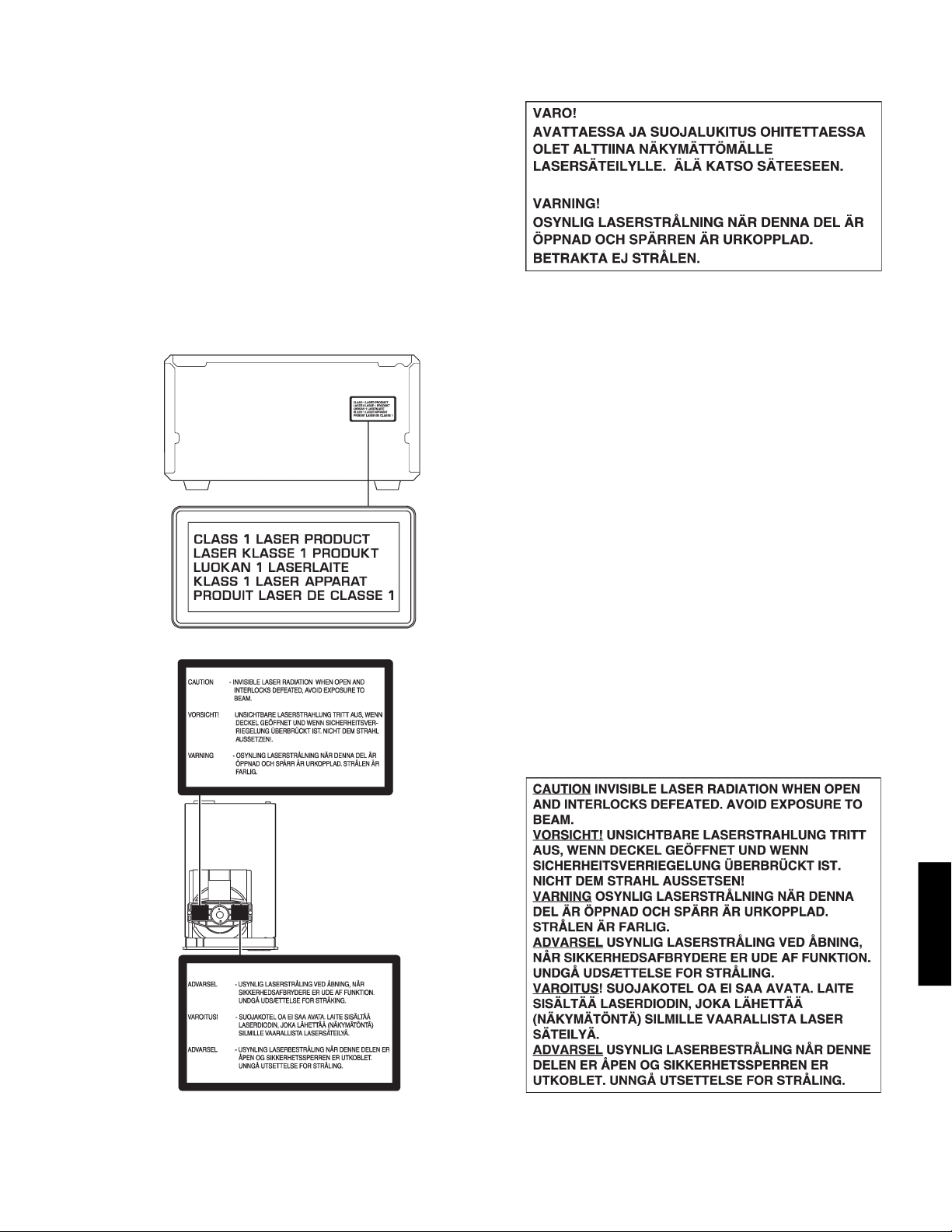
Laser Diode Properties
Type: GaAlAs
Wave length: 780 nm
Emission duration: continuous
Laser output: max. 44.6 µW *
* This output is the value measured
at a distance of about 200 mm from
the objective lens surface on the
optical pick-up block.
WARNING
CDX-E410
CDX-497/CDX-397
CDX-E410
3
CDX-E410
■ PREVENTION OF ELECTROSTATIC DISCHARGE
Some semiconductor (solid state) devices can be damaged easily by static electricity. Such components commonly are called
Electrostatically Sensitive (ES) Devices. Examples of typical ES devices are integrated circuits and some field-effect transistors
and semiconductor “chip” components. The following techniques should be used to help reduce the incidence of component
damage caused by electro static discharge (ESD).
1. Immediately before handling any semiconductor component or semiconductor-equipped assembly, drain off any ESD on
your body by touching a known earth ground. Alternatively, obtain and wear a commercially available discharging ESD wrist
strap, which should be removed for potential shock reasons prior to applying power to the unit under test.
2. After removing an electrical assembly equipped with ES devices, place the assembly on a conductive surface such as
aluminum foil, to prevent electrostatic charge buildup or exposure of the assembly.
3. Use only a grounded-tip soldering iron to solder or unsolder ES devices.
4. Use only an anti-static solder removal device. Some solder removal devices not classified as “anti-static (ESD protected)”
can generate electrical charge sufficient to damage ES devices.
5. Do not use freon-propelled chemicals. These can generate electrical charges sufficient to damage ES devices.
6. Do not remove a replacement ES device from its protective package until immediately before you are ready to install it. (Most
replacement ES devices are packaged with leads electrically shorted together by conductive foam, aluminum foil or compa-
rable conductive material).
7. Immediately before removing the protective material from the leads of a replacement ES divice, touch the protective material
to the chassis or circuit assembly into which the device will be installed.
CAUTION: Be sure no power is applied to the chassis or circuit, and observe all other safety precautions.
8. Minimize bodily motions when handling unpackaged replacement ES devices. (Otherwise harmless motion such as the
brushing together of your clothes fabric or the lifting of your foot from a carpeted floor can generate static electricity (ESD)
sufficient to damage an ES device).
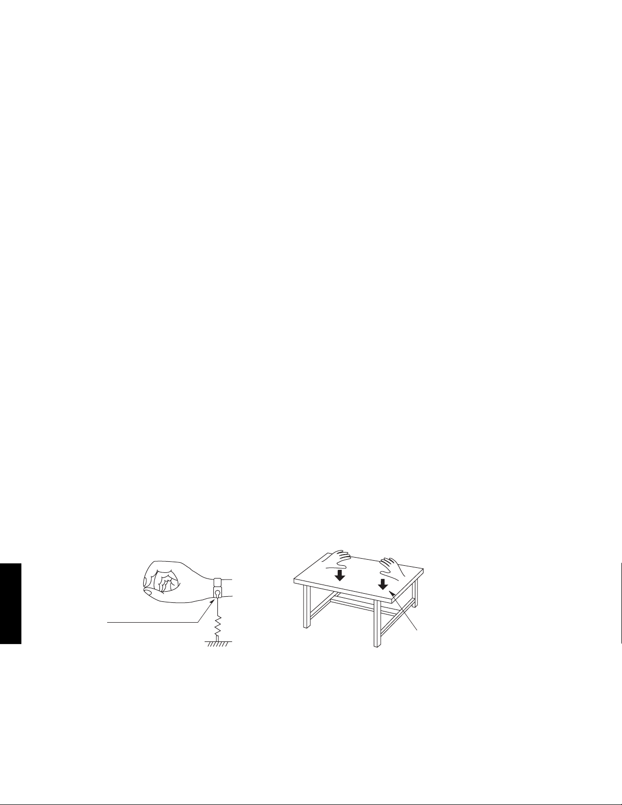
Grounding for electrostatic breakdown prevention
1. Human body grounding.
Use the antistatic wrist strap to discharge the static electricity from your body.
2. Work table grounding.
Put a conductive material (sheet) or steel sheet on the area where the optical pickup is placed and ground the sheet.
Caution:
The static electricity of your clothes will not be grounded through the wrist strap. So take care not to let your clothes touch the
optical pickup.
Anti-static wrist strap
CDX-E410
1M-ohms
Conductive material
(sheet) or steel sheet
4
215 (8-7/16")
100 (3-15/16")
8
(5/16")
108 (4-1/4")
327 (12-7/8")
2
(1/16")
5
(3/16")
334 (13-1/8")
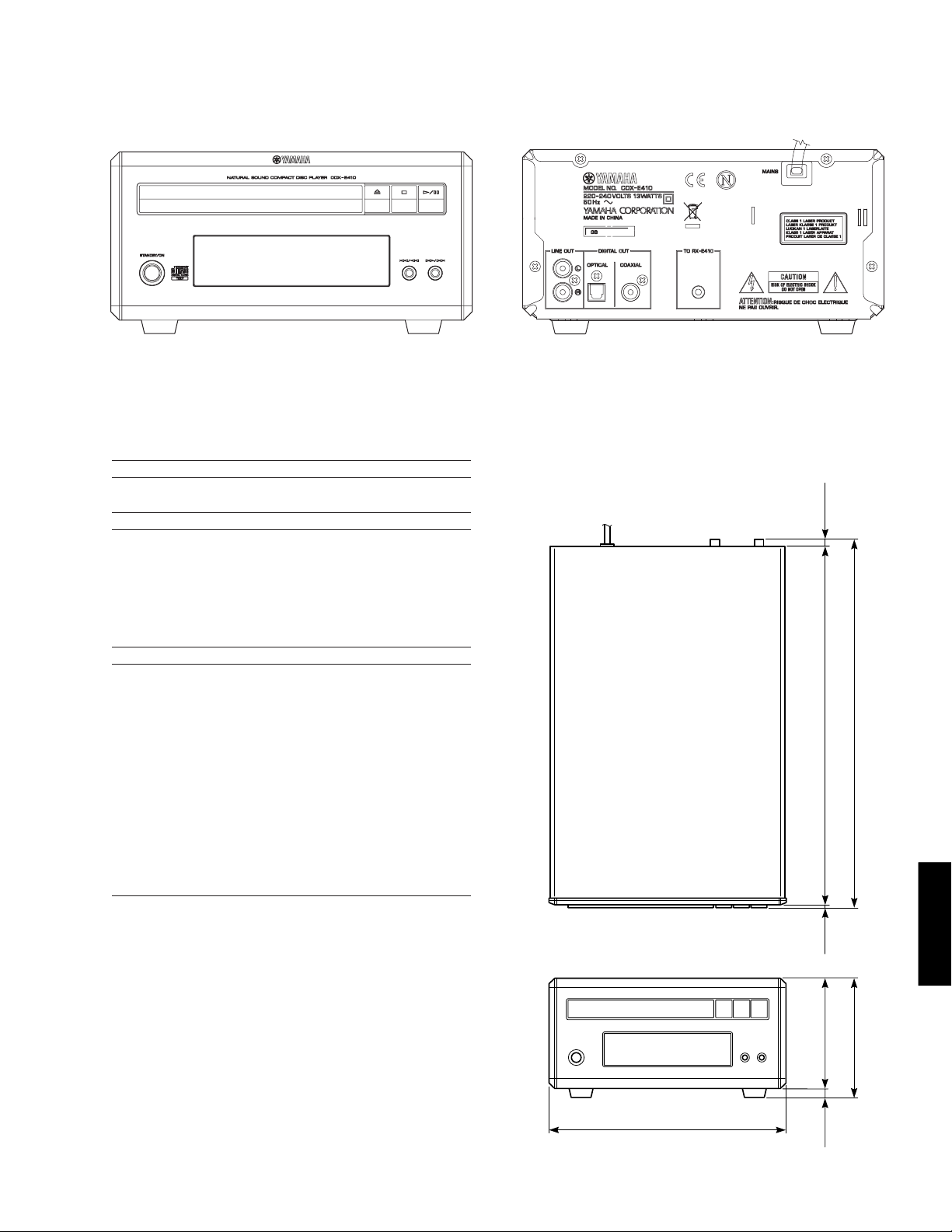
■ FRONT PANEL ■ REAR PANEL
CDX-E410
B, G models
■ SPECIFICATIONS
■ PLAYBACK SYSTEM
CD, CD-R/RW
■ AUDIO PERFORMANCE
Signal to Noise (1 kHz)
............................................................................... 105 dB or more
Dynamic Range (1 kHz)
................................................................................. 95 dB or more
Distortion and Noise (1 kHz)
............................................................................... 0.003 % or less
B, G models
• DIMENSIONS
CDX-497/CDX-397
■ GENERAL
Dimensions (W x H x D)
........................... 215 x 108 x 334 mm (8-7/16” x 4-1/4” x 13-1/8”)
Weight
............................................................ Approx. 2.8 kg (6 lbs. 3 oz)
Finish
Black color ........................................................................ G model
Silver color .................................................................. B, G models
Power Supply
B, G models ................................................. AC 220-240 V, 50 Hz
Power Consumption
.................................................................................. Approx. 13 W
Accessories
............................................................ Audio pin cable (1.5 m) x 1
* Specifications are subject to change without notice.
B .......... British model G ...... European model
CDX-E410
Unit: mm (inch)
5
CDX-E410
■ INTERNAL VIEW
4
2
5
1 3
1
FRONT (2) P.C.B.
2
MAIN (2) P.C.B.
3
MAIN (1) P.C.B.
4
CD Mechanism
5
FRONT (1) P.C.B.
■ REPAIR NOTES
None of the components of the following units can be supplied separately.
Each unit must be replaced as a whole in case of a failure.
• CD Mechanism
• MAIN P.C.B.
• FRONT P.C.B.
■ HOW TO MANUALLY EJECT THE TRAY
a. Turn the unit bottom up.
b. Using a flatblade screwdriver, turn the loading cam 90 degrees in the direction indicated by an arrow in the figure.
c. Gently pull the tray out.
Loading Cam
Flatblade Screwdriver
CDX-E410
Tr ay
Tr ay
6
■ DISASSEMBLY PROCEDURES
See REPLACEMENT PARTS LIST for item numbers.
CDX-E410
→ Remove 4 screws. [60] (4 on side)
→ Remove 4 screws. [51]
(4 on rear side)
→ Lift top cover from rear side to remove.
→ Open tray. (See "
→ Unlock tray lid and close tray.
→ Remove CN52. (MAIN (1) P.C.B.)
→ Remove 2 screws. [53]
→ Remove 2 screws. [51]
→ Unlock front panel ass'y from frame
→ Remove front panel ass'y.
Front Panel Ass'y
EJECT THE TRAY
(Front panel ass'y to side frame)
(Front panel ass'y to bottom frame)
by releasing successively 2 snaps.
(2 on the side)
FRONT (1) P.C.B. [32 (1)]
→ Remove 10 snaps.
(P.C.B. to front panel ass'y)
→ Remove FRONT (1) P.C.B..
HOW TO MANUALLY
")
Top Cabinet [28]
CD Mechanism [36]
→ Open tray. (See "
EJECT THE TRAY
→ Unlock tray lid and close tray.
→ Remove CN21-23.
→ Remove 4 screws. [52]
(CD mechanism to P.C.B.
support)
→ Remove CD mechanism.
HOW TO MANUALLY
")
Mounting
Dismounting
MAIN (2) P.C.B. [34 (2)]
→ Remove 1 screw. [61]
(P.C.B. to rear panel)
→ Remove MAIN (2) P.C.B.
which is connected directly
to the lower P.C.B. with
connectors.
MAIN (1) P.C.B. [34 (1)]
→ Remove CN21-23, CN41
and CN52 (MAIN (1) P.C.B.).
→ Remove 3 screws. [59]
(P.C.B. to rear panel)
→ Remove 1 screw. [54]
(P.C.B. to bottom frame)
→
Remove 1 screw. [58]
(P.C.B. to bottom frame)
→ Remove MAIN (1) P.C.B..
FRONT (2) P.C.B. [32 (2)]
→ Remove CN41 (FRONT (2)
P.C.B.) and CN41 (MAIN (1)
P.C.B.).
→ Remove 1 screw. [56]
(P.C.B. to bottom frame)
→ Remove 2 screws. [57]
(P.C.B. to bottom frame)
→ Remove FRONT (2) P.C.B..
CDX-497/CDX-397
• Cable Connections
CN41
(FRONT (2) P.C.B.)
FRONT (2) P.C.B.
BN41
FRONT (1) P.C.B.
CN41
(MAIN (1) P.C.B.)
CN21
MAIN (2) P.C.B.
MAIN (1) P.C.B.
CN22CN23
CN52
(FRONT (1) P.C.B.)
CDX-E410
CN52 (MAIN (1) P.C.B.)
CD Mechanism
7
CDX-E410
■ TEST MODE
With CDX-E410 alone, it is not possible to start the TEST mode.
Be sure to prepare, receiver (RX-E410), system control cable and remote control.
Preparation and precautions before starting the operation
Connect the “TO RX-E410” terminal of the CDX-E410 to the “TO CDX-E410” terminal of the RX-E410 with the system
control cable.
• Starting Test Mode
a. Connect the power cable of CDX-E410 and RX-
E410 to the AC outlet.
b. Press the “STANDBY/ON” key of the CDX-E410.
RX-E410 and CDX-E410 will start up.
c. Press the “FILE/A-E” key of the remote control while
simultaneously pressing “STOP” key of the CDXE410.
When in the TEST mode, the “TEST MODE” is displayed for 2 seconds.
2 seconds
Starting
TEST mode
This part is always displayed
when in the TEST mode.
2. Function list of remote control keys.
Panel key Function
WW
W
(PLAY)
WW
DD
D (PAUSE)
DD
AA
A
(STOP)
AA
TT
T
(SKIP-)
TT
YY
Y (SKIP+)
YY
TIME/INFO
RANDOM
*1 Check FL display
The display condition varies as shown below according to the “TIME/INFO” key of the remote control.
Playback.
Pause.
Stop.
Move traverse reverse.
Move traverse forward.
Check FL display. (*1)
Spindle servo on/off.
Initial display
Icon (left)
1. Function list of panel keys.
Panel key Function
FF
F (OPEN/CLOSE)
FF
WW
DD
W /
D (PLAY/PAUSE)
WW
DD
AA
A (STOP)
AA
TT
EE
T /
E (SKIP-/SEARCH-)
TT
EE
RR
YY
R /
Y (SKIP+/SEARCH+)
RR
YY
CDX-E410
• Canceling Test Mode
Press the “STANDBY/ON” key of the CDX-E410.
Tray open/close.
Playback/Pause.
Stop.
Move traverse reverse.
Move traverse forward.
Icon (right)
Pattern 1
Pattern 2
Pattern 3
Pattern 4
Pattern 5
Pattern 6
Pattern 7
Icon (left)
8
■ IC DATA
IC21 : TC94A54 (MAIN P.C.B)
DSP
* No replacement part available.
DVSS3
RO
DVDD3
DVR
LO
DVSS3
VSS3
VDD3
VDDM
VSS1S
BUS0
BUS1
BUS2
BUS3
BUCK
/CCE
/RST
STBY
VDDT
FGIN
IO0
IO1
TESTD
VSSP
VCOI
26
27
28
29
30
31
32
33
34
35
36
37
38
39
40
41
42
43
44
45
46
47
48
49
50
XVDD3XOXI
ANA
LPF
PULL-UP
VDDP
CPU
I/F
TESTC
1-bit
DAC
PIO0
XVSS3
CLOCK
GEN
PIO1
VDD1
VSS1S
GPIN
ZDET
ADRRESS CIRCUIT
16k
DIGITAL
OUT
PIO3
DOUT
RAM
AUDIO
OUT
AOUT
CIRCUIT
CORRECTION
PIO2
SFSY
IPF
SUBCODE
DEMOCULA
TION
CDRCUIT
BCKO
LRCKO
SBSY
SBOK
AIN
DMO
PMO
PWM
SERVO
CONTROL
ROM
DIGITAL EQ
AUTO ADJ
RAN
CAV SERVO
SYNC SIGNAL PROTECTION
EFM DEMODULATION
BCKI
LRCKI
VDD1S
VREF
5-bit
R-2R DAC
AWRC
VSS1S
TRO
FOO
CLV SERVO
TMAX
AWRC
PVDD3
AVDD3
PLL
PDO
TEZI
TEI
10-bit
SAR ADC
LPPN
TMAX
SBAD/RFDC
FEI
RFRP
RF
BLOCK
EFM SLICE
VCO
LPFO
PVREF
VCOF
AVSS3
TE
FE
APC
RF
RFDC
AGC
VRO
RFEQ
RFRP
VCOREF
RFZI
12345678910111213141516171819202122232425
75747372717069686766656463626160595857565554535251
PVSS3
100
99
98
97
96
95
94
93
92
91
90
89
88
87
86
85
84
83
82
81
80
79
78
77
76
FTE
TNI
TPI
FPI1
FPI2
PNI1
PNI2
RVSS3
MDI
LDO
RVDD3
PNSEL
RFO
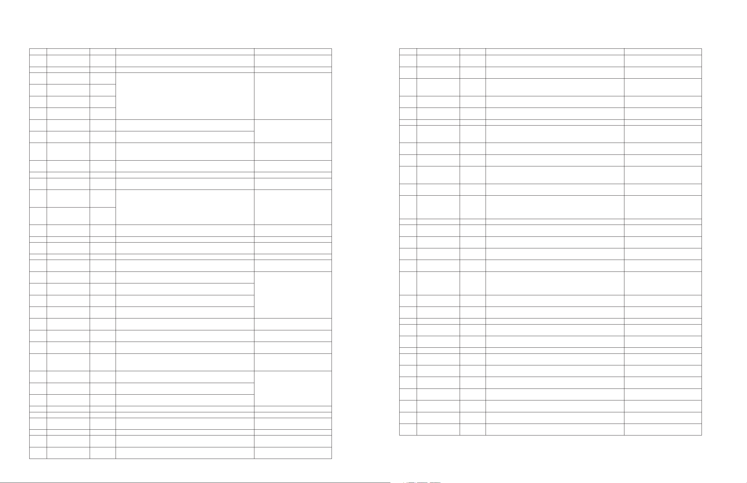
Pin No. Pin name Description Remark
1
2
3
RFZI
AVSS3
RFRP
I/O
I
3AI/F
–
O
Input pin for the RF ripple zero-cross signal.
Grounding pin for 3.3V analog circuits.
RF ripple signal output pin.
To be connected to the RFRP via
0.033 uF.
–
–
3AI/F
4
FEI
O
Focus error signal input pin.
3AI/F
5
SBAD/RFDC
O
Subbeam addition signal input pin.
Monitor pin for various signals.
3AI/F
6
TEI
O
Tracking error signal input pin.
3AI/F
7
TEZI
I
Input pin for tracking error signal zero-cross.
3AI/F
8
9
AVDD3
FOO
–
Supply voltage pin for 3.3V analog circuit.
O
Forcus equalizer output pin.
To be connected to the TEI via
0.033 uF.
–
–
3AI/F
10
TRO
O
Tracking equalizer output pin.
–
3AI/F
11
VREF
O
3AI/F
Analog reference supply voltage pin.
Connected to the VRO and
PVREF within the IC.
To be connected 0.1 uF.
12
13
FMO
DMO
O
3AI/F
O
Speed error/feed equalizer output pin.
Disc equalizer output pin.
PWM ternary output (AVDD3,
GND, and VREF).
3AI/F
14
SBSY
(SPCK)
O
3I/F
Pin for outputting the subcode block sync signal. It is “H” at
position S1 when the subcode sync signal is detected.
“H” at S1 when Subcode Sync is
detected.
(CD Processor Status Read Clock (176.4 kHz) output)
15
SBOK
(FOK)
(CLCK)
(MBOV)
O
3I/F
Pin for outputting the CRCC check result of a subcode Q data
check. It is “H” when the check result is OK.
(Focus OK signal)
(Input/output pin for the clock used in reading the subcode P
–
to W data.)
(CD Buffer memory overflow output)
16
IPF
(SPDA)
O
3I/F
Correction flag output pin.
“H” if the AOUT pin outputs an uncorrectable symbol in C2
–
correction.
(CD Processor Status signal output)
17
18
19
20
21
22
23
SFSY
(EMPH)
(LOCK)
(MONIT)
ZDET
(DATA)
(COFS)
GPIN
VSS1
VDD1
XVSS3
XI
O
3I/F
O
3I/F
I/O
3I/F
–
–
–
I
Pin for outputting the playback frame sync signal.
(Emphasis fiag output pin. ENPH on: “H”. EMPH off: “L”. The
output polarity can be switched, using a command.)
(LOCk signal)
(Pin for monitoring signals in the DSP.)
Output pin for zero detection flag for the 1-bit DAC.
(Pin for outputting subcode P to W data)
(Error Correstion Frame Clock 7.35 kHz output)
General-purpose I/O (DSP)
1.5V grounding pin dedicated to the Digital circuit.
1.5V supply voltage pin dedicated to the Digital circuit.
Grounding pin for the system clock oscillation circuit.
Input pin for the system clock oscillation circuit.
7.35kHz (At this pin, flags in the
DSP and PLL-circuit clock can be
monitored, using microcontroller
commands. The pin also outputs
text data serially.)
Valid also for 1-bit DAC external
inputs.
General-purpose I/O (input after a
reset).
–
–
–
–
3AI/F
24
XO
O
Output pin for the system clock oscillation circuit.
Input to the internal MCK.
3AI/F
25
26
27
28
XVDD3
DVSS3
RO
DVDD3
–
–
O
3AI/F
–
3.3V supply voltage pin for the system clock oscillation circuit.
Grounding pin for the 1-bit DAC.
Output pin for normal R-channel data for the 1-bit DAC.
3.3V supply voltage pin for the 1-bit DAC.
No capacitor is required at the
DVR pin unless the built-in 1-bit
DAC is used.
–
–
3.3V must be applied across the
29
DVR
O
Reference voltage pin for the 1-bit DAC.
DVDD3 and DVSS3 pins, however.
30
LO
O
Output pin for normal L-channel data for the 1-bit DAC.
–
3AI/F
31
32
33
DVSS3
VSS3
VDD3
–
Grounding pin for the 1-bit DAC.
–
3.3V grounding pin dedicated to the I/F circuit
–
3.3V supply voltage pin dedicated to the I/F circuit.
–
–
CDX-E410
9
CDX-E410
34
35
36
37
38
39
40
41
42
43
44
45
46
47
48
49
50
51
52
53
54
55
56
57
58
59
60
61
62
63
64
65
66
67
68
69
VDDM
VSS1
BUS0
BUS1
BUS2
BUS3
BUCK
/CCE
/RST
STBY
VDDT
FGIN
IO0A
(/HSO)
IO1A
(/UHSO)
TESTD
VSSP
VCOI
VDDP
TESTC
PIO0
PIO1
PIO2
PIO3
DOUT
AOUT
BCK
LRCK
AIN
BCKI
LRCKI
VDD1
VSS1
AWRC
PVDD3
PDO
TMAX
–
–
I/O
3I/F
I/O
3I/F
I/O
3I/F
I/O
3I/F
I
3I/F
I
3I/F
I
3I/F
I
3I/F
–
I
3AI/F
I/O
3I/F
I/O
3I/F
I
3I/F
–
O
1.5AI/F
–
I
3I/F
I/O
3I/F
I/O
3I/F
I/O
3I/F
I/O
3I/F
O
3I/F
O
3I/F
O
3I/F
O
3I/F
I
3I/F
I
3I/F
I
3I/F
–
–
O
3AI/F
–
O
3AI/F
O
3AI/F
1.5V supply voltage pin dedicated to the DSP/1Mbit SRAM
circuit.
1.5V groundind pin dedicated to the DSP/1Mbit SRAM circuit.
Data input/output pin for the microcontroller interface.
Clock input pin for the microcontroller interface.
Chip enable signal input pin for the microcontroller interface.
BUS3 to BUS0 are active if this pin is “L”.
Reset signal input pin. The internal registers and servo section
registers are reset, respectively, when the reset signal is “L”
and on the positive-going edge of the reset signal.
STANDBY control pin dedicated to the DSP/1Mbit SRAM
circuit.
3.3V supply voltage pin dedicated to the Digital I/O circuit.
FG signal input pin for CAV.
CLV: “L”. CAV: FG input.
Genelal-purpose input/output pins.
(Pin for outputting the playback speed mode flag.)
DSP/Test input pin. Usually fixed at “L”.
1.5V grounding pin dedicated to the DSP/VCO circuit.
PD output pin dedicated to the DSP/VCO circuit.
1.5V supply voltage pin dedicated to the DSP/VCO circuit.
CD/Test input pin. Usually fixed at “L”.
General-purpose I/O (CD/DSP)
General-purpose I/O (CD/DSP)
General-purpose I/O (DSP)
General-purpose I/O (DSP)
Digital-out output pin. Digital data for up to double speed can
be output when a frequency of 16.9344 MHz is used.
Audio data output pin. Which bit is first (MSB first or LSB first)
can be selected, using a command.
Bit clock output pin. 32fs, 48fs, and 64fs can be selected,
using a command.
LR channel clock output pin. L for the L-channel and “H” for
the R-channel. The output polarity can be inverted, using a
command.
1-bit DAC external input: AIN
1-bit DAC external input: BCKI
1-bit DAC external input: LRCKI
1.5V supply voltage pin dedicated to the DSP circuit.
1.5V grounding pin dedicated to the DSP circuit.
VCO control pin for active wide range.
3.3V supply voltage pin dedicated to the PLL circuit.
Pin for outputting a phase difference signal between the EFM
signal and PLCK signal.
Pin for outputting the result of TMAX detection.
The TMAX pin output the same signal.
RemarkPin No. Pin name FunctionPin name
–
–
To be fixed at “H” or “L” when communication is not in progress, so
that the pin will not become HiZ.
To be fixed at “H” when communication is not in progress, so that
the pin will not become HiZ.
To be connected to 0.1 uF.
–
–
–
Genelal-purpose I/O (input after a
reset).
The playback speed mode flag
output can be switched, using
command bits.
–
–
–
–
–
General-purpose I/O (input after a
reset).
As per CP-1201
–
Normal speed: 32fs = 1.4112 MHz
Normal speed: 44.1kHz
1-bit DAC external input
Controllable in CLV/CAV.
–
Quaternary output (PVDD3, HiZ,
VSS, and PVREF).
Ternary output (PVDD3, VSS, and
Hiz).
70
71
72
73
74
75
76
77
78
79
80
81
82
83
84
85
86
87
88
89
90
91
92
93
94
95
96
97
98
99
100
LPFN
LPFO
PVREF
VCOF
VCOREF
PVSS3
SLCO
RFI
RFRPI
RFEQO
RESIN
VRO
VMDIR
TESTR
INVSEL
AGCI
AGCI
RFO
PNSEL
EQSET
RVDD3
LDO
MDI
RVSS3
FNI2
FNI1
FPI2
FPI1
TPI
TNI
FTE
I/OPin No. Pin name Description Remark
I
3AI/F
3AI/F
3AI/F
3AI/F
3AI/F
3AI/F
3AI/F
3AI/F
3AI/F
3AI/F
3AI/F
3AI/F
3AI/F
3AI/F
3AI/F
3AI/F
3AI/F
3AI/F
3AI/F
3AI/F
3AI/F
3AI/F
3AI/F
3AI/F
3AI/F
3AI/F
Pin for receiving an inverted output of the PLL-circuit low-pass
filter amp.
O
Pin for the PLL-circuit low-pass filter amp output.
–
1.65V reference supply voltage pin dedicated to the PLL
circuit.
O
VCO filter pin.
I
Input pin for the VCO center frequency reference level.
–
3.3V grounding pin dedicated to the PLL circit.
O
EFM slice level output pin.
For both analog and digital slice modes, the output impedance
= 2.5 k-ohms.
I
RF signal input pin.
The input resistance can be selected, using a command.
I
RF ripple signal input pin.
O
RF equalizer circuit output pin.
I
Pin for connecting a reference current generating resistance.
O
1.65V reference voltage output pin.
–
Reference voltage poutput pin for the APC circuit.
O
LPF pin for RFEQO offset correction.
I
Test pin, usually fixed at “L”.
I
Pin for RF signal amplitude adjustment amp input.
I
RF signal peak detsction input pin.
O
RF signal generation amp output pin.
I
Test pin, usually fixed at “H”.
O
External connection pin for the RF signal equalizer.
–
3.3V supply voltage pin for the Rfamp core section.
O
Laser diode amp output pin.
I
Monitor photodiode amp input pin.
–
3.3V grounding pin for the RF amp core section.
I
Main beam input pin.
Connected to PIN diode C.
I
Main beam input pin.
Connected to PIN diode A.
I
Main beam input pin.
Connected to PIN diode D.
I
Main beam input pin.
Connected to PIN diode B.
I
Subbeam input pin.
Connected to PIN diode F.
I
Subbeam input pin.
Connected to PIN diode E.
O
Focus /tracking signal output.
(Test pin for servo characteristic measurement.)
Note: “3AI/F : 3V circuit analog input/output pin.”
“3I/F : 3V circuit digital input/output pin.”
“1.5AI/F : 1.5V circuit analog input/output pin.”
The resistance side is connected.
See an applicable circuit diagram.
The capacitor side is connected.
See an spplicable circuit diagram.
Connected to the VREF and PVREF
within the IC.
A 0.1 uF capacitor is connected.
–
To be connected to the PVREF if
the AWRC is not used.
–
A capacitor to be connected is selected according to the servo operation band.
Zin: 20 k-ohms, 10 k-ohms, 5 kohms
–
To be connected to the RFRPI via
0.1 uF and to the RFI via 4700 pF
or higher.
To be connected to 22 k-ohms
and 680 pF in parallel.
Connected to the VREF and
PVREF within the IC
To be connected to 0.1uF anf 100
uF.
To be connected to 0.1uF.
To be connected to 0.015 uF or
higher.
–
–
–
To be connected directly to the
RFDCI.
To ne connected to the AGCI via
0.1 uF.
To be kept open when the RFEQ
is used.
–
Reference to 178 mV (typ.)
–
–
–
–
–
–
–
Switchable using a command.
10
 Loading...