

Yamaha AO8-DA8, AO8 Service Manual
ANALOG OUTPUT BOX
SERVICE MANUAL
• AO8-DA8
011506
PA
200004**-250000
CONTENTS
REVISED PAGE LIST ··························································· 2-1
SPECIFICATIONS································································· 3-1
PANEL LAYOUT···································································· 3-2
DIMENSIONS········································································ 3-3
CONNECTOR CIRCUIT DIAGRAM ········································· 4
BLOCK DIAGRAM···································································· 6
DISASSEMBLY PROCEDURE················································· 7
LSI PIN DESCRIPTION·························································· 11
IC BLOCK DIAGRAM ····························································· 14
CIRCUIT BOARDS································································· 15
INSPECTION·········································································· 20
TEST PROGRAM··································································· 22
ERROR MESSAGES······························································ 27
PARTS LIST
CIRCUIT DIAGRAM
HAMAMATSU, JAPAN
0.27K-
K Printed in Japan '00.09
****
AO8
REVISED PAGE LIST
ITEM
SPECIFICATIONS
PANEL LAYOUT
DIMENSIONS
CONNECTOR CIRCUIT DIAGRAM
INSPECTION
TEST PROGRAM
ERROR MESSAGES
<
PARTS LIST>
ITEM
OVERALL ASSEMBLY
SIDE PANEL ASSEMBLY
MOTHER ASSEMBLY
ELECTRICAL PARTS
PAGE
3-1
3-2
3-3
5
20~21
22~26
27
PAGE
3, 4
5
6
7~10
<
CIRCUIT DIAGRAM>
ITEM
IFC3 CIRCUIT DIAGRAM 002
IPC2 CIRCUIT DIAGRAM
AOCOM CIRCUIT DIAGRAM 002
003
004
005
006
007
003
PAGE
9
10
11
12
13
14
15
18
19
2-1
AO8
2-2
WARNING: CHEMICAL CONTENT NOTICE!
The solder used in the production of this product contains LEAD. In addition, other electrical/electronic and/or plastic (where
applicable) components may also contain traces of chemicals found by the California Health and Welfare Agency (and possibly
other entities) to cause cancer and/or birth defects or other reproductive harm.
DO NOT PLACE SOLDER, ELECTRICAL/ELECTRONIC OR PLASTIC COMPONENTS IN YOUR MOUTH FOR ANY REASON
WHAT SO EVER!
Avoid prolonged, unprotected contact between solder and your skin! When soldering, do not inhale solder fumes or expose eyes
to solder/flux vapor!
If you come in contact with solder or components located inside the enclosure of this product, wash your hands before handling
food.
IMPORTANT NOTICE
This manual has been provided for the use of authorized Yamaha Retailers and their service personnel. It has been assumed that
basic service procedures inherent to the industry, and more specifically Yamaha Products, are already known and understood by
the users, and have therefore not been restated.
WARNING: Failure to follow appropriate service and safety procedures when servicing this product may result in personal
injury, destruction of expensive components and failure of the product to perform as specified. For these
reasons, we advise all Yamaha product owners that all service required should be performed by an authorized
Yamaha Retailer or the appointed service representative.
IMPORTANT: This presentation or sale of this manual to any individual or firm does not constitute authorization, certification,
recognition of any applicable technical capabilities, or establish a principal-agent relationship of any form.
The data provided is belived to be accurate and applicable to the unit(s) indicated on the cover. The research engineering, and
service departments of Yamaha are continually striving to improve Yamaha products. Modifications are, therefore, inevitable and
changes in specification are subject to change without notice or obligation to retrofit. Should any discrepancy appear to exist,
please contact the distributor's Service Division.
WARNING: Static discharges can destroy expensive components. Discharge any static electricity your body may have
accumulated by grounding yourself to the ground bus in the unit (heavy gauge black wires connect to this bus).
IMPORTANT: Turn the unit OFF during disassembly and parts replacement. Recheck all work before you apply power to the
unit.
WARNING
Components having special characteristics are marked and must be replaced with parts having specification equal to those
originally installed.
IMPORTANT NOTICE FOR THE UNITED KINGDOM
Connecting the Plug and Cord
IMPORTANT. The wires in this main lead are coloured in
accordance with the following code:
BLUE: NEUTRAL
BROWN: LIVE
As the colours of the wires in the main lead of this apparatus may not
correspond with the coloured markings identifying the terminals in
your plug, proceed as follows:
The BLUE wire must be connected to the terminal that is marked with
the letter N (or coloured BLACK).
The BROWN wire must be connected to the terminal that is marked
with the letter L (or coloured RED).
Be certain that neither core is connected to the earth terminal of the
three pin plug.
SPECIFICATIONS
AO8
3-1
Sampling frequency (external sync)
Power supply
Power consumption
Dimensions (W x H x D)
Weight
Operating temperature
Power cable length
Cooling fan speed
Accessories
39.69 kHz – 50.88 kHz
USA and Canada: 120 V, 60 Hz
Others: 230 V, 50 Hz
120 W
480 mm x 141.5 mm x 466.8 mm
15.4 kg
10 – 35 ˚C
2.1 m
always fixed
Connection cable (68-pin, D-sub, half-pitch) x 1, Length: 3 m
I/O connectors
INPUT A, B, C
WORD CLOCK IN
WORD CLOCK OUT
Level
RS-422
TTL/75 Ω (ON/OFF)
TTL/75 Ω
Type
D-sub, half-pitch, 68-pin connector (female)
BNC Connector
BNC Connector
Digital I/Os
Card
LMY4-AD
Input
Channel 1 – 4
Slots
*
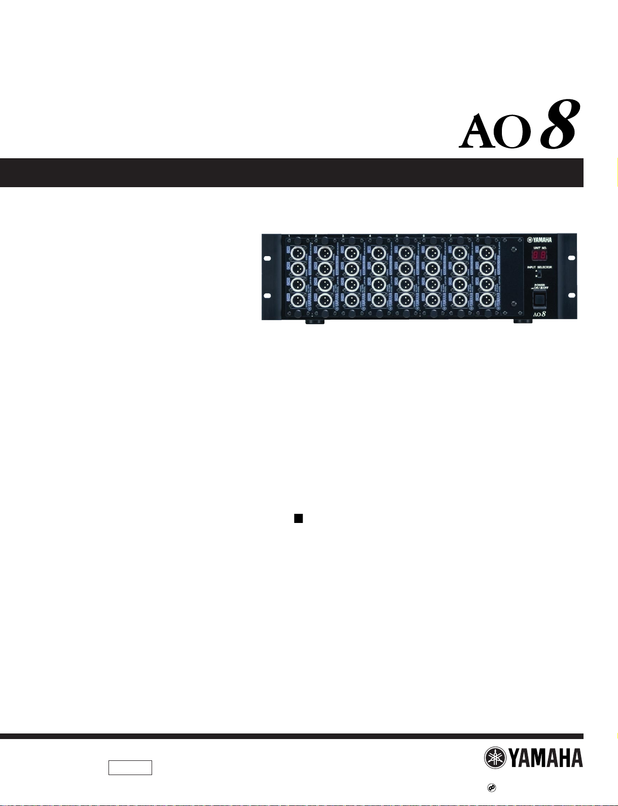
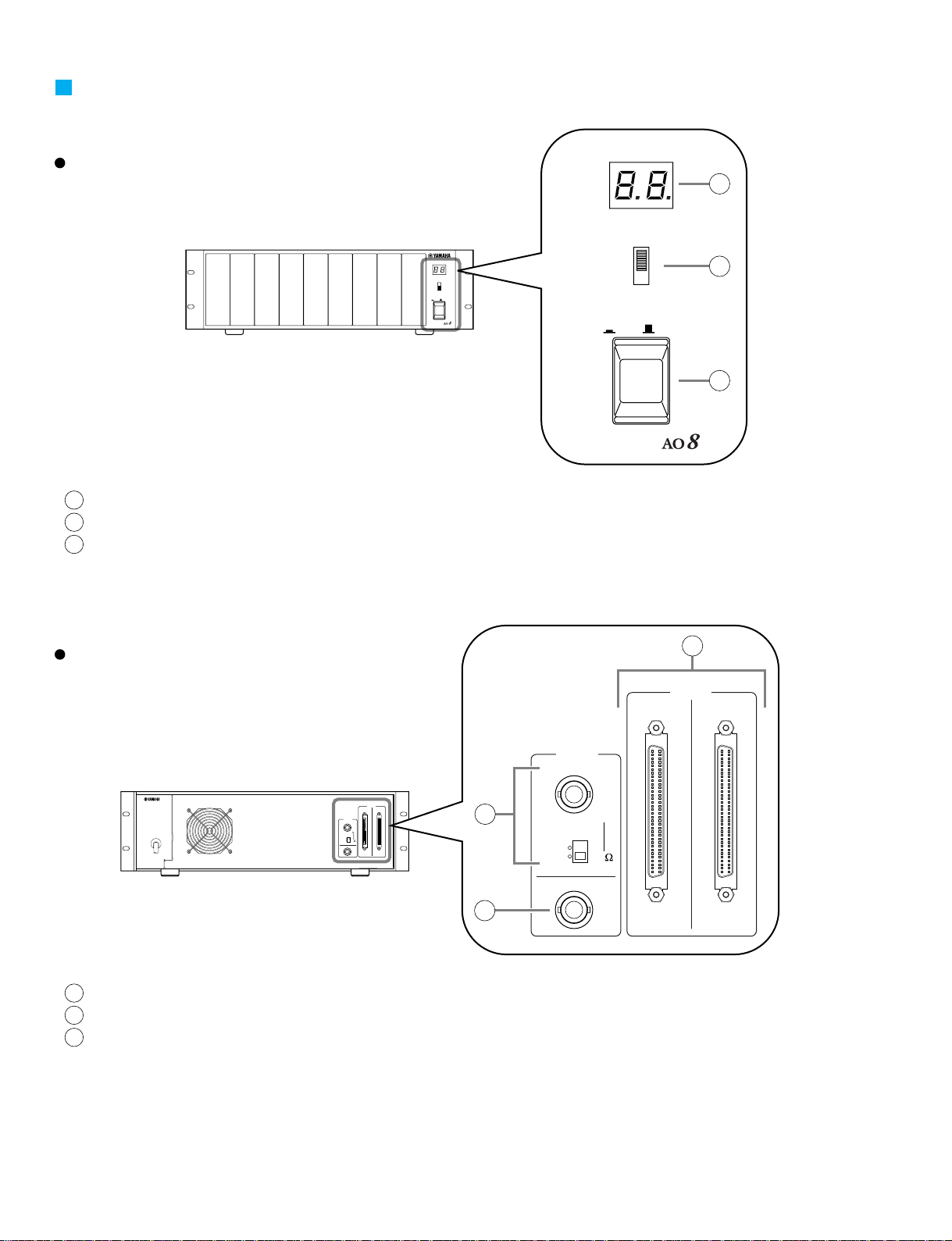
The illustration shows the AO8 analog output box.
1234567
UNIT NO.
INPUT SELECTOR
A
B
POWER
ON/ OFF
8
ANALOG OUTPUT BOX
OUTPUT UNIT ID
INPUT SELECTOR
A
B
POWER
ON/ OFF
ANALOG OUTPUT BOX
75
IN
BA
INPUT
ON
OFF
OUT
WORD
CLOCK
BA
INPUT
ON
OFF
OUT
WORD
CLOCK
75
IN
1
2
3
5
6
4
1
OUTPUT UNIT ID indicator
2
INPUT SELECTOR switch
3
POWER ON/OFF
4
INPUT connectors A and B
5
WORD CLOCK IN jack, ON/OFF switch
6
WORD CLOCK OUT jack
Front Panel
Rear Panel
AO8
3-2
PANEL LAYOUT
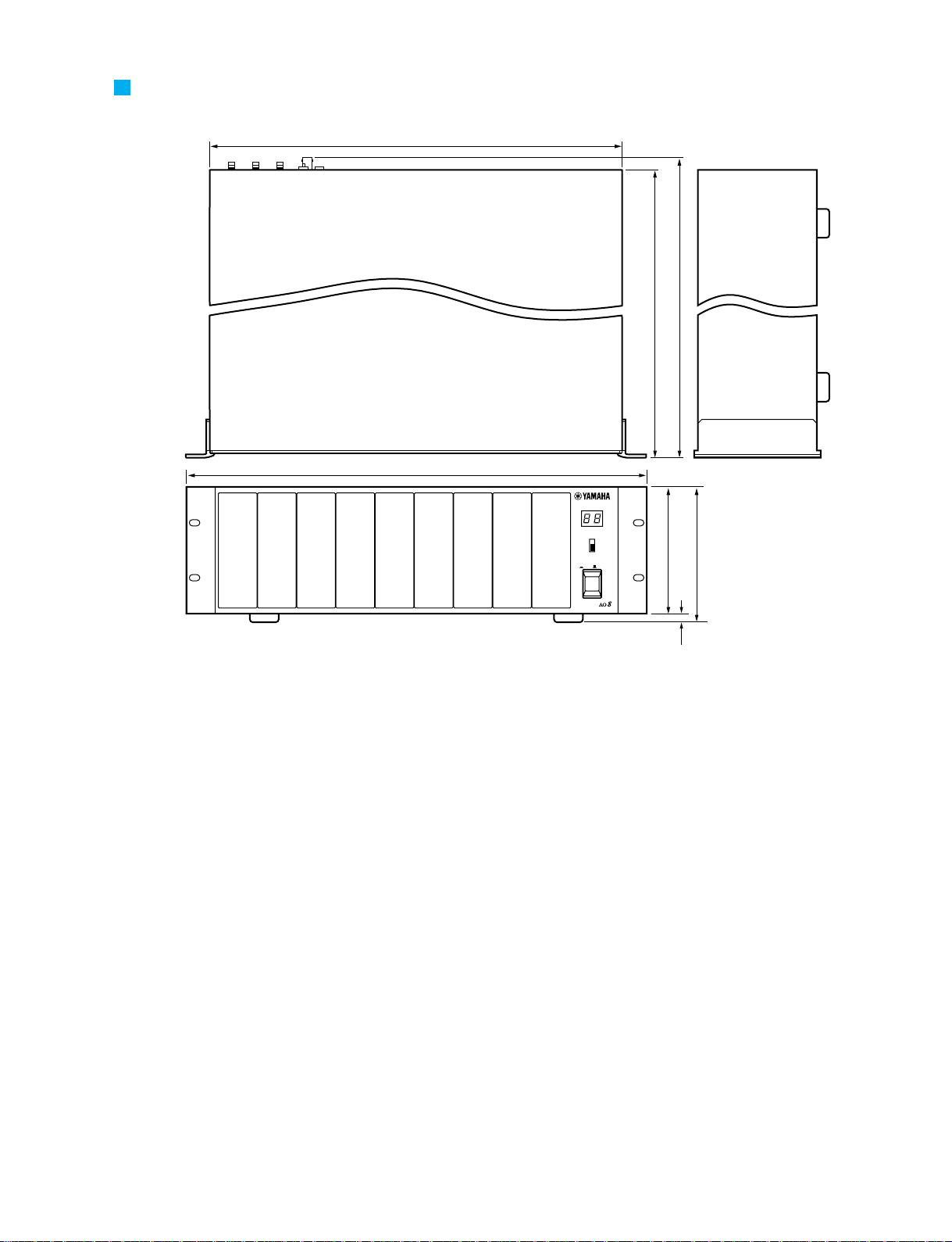
455
466.8
480
430
132 (3U)
141.5
OUTPUT UNIT ID
INPUT SELECTOR
A
B
POWER
ON/ OFF
1234567 8
ANALOG OUTPUT BOX
9.5
Unit: mm
DIMENSIONS
AO8
3-3
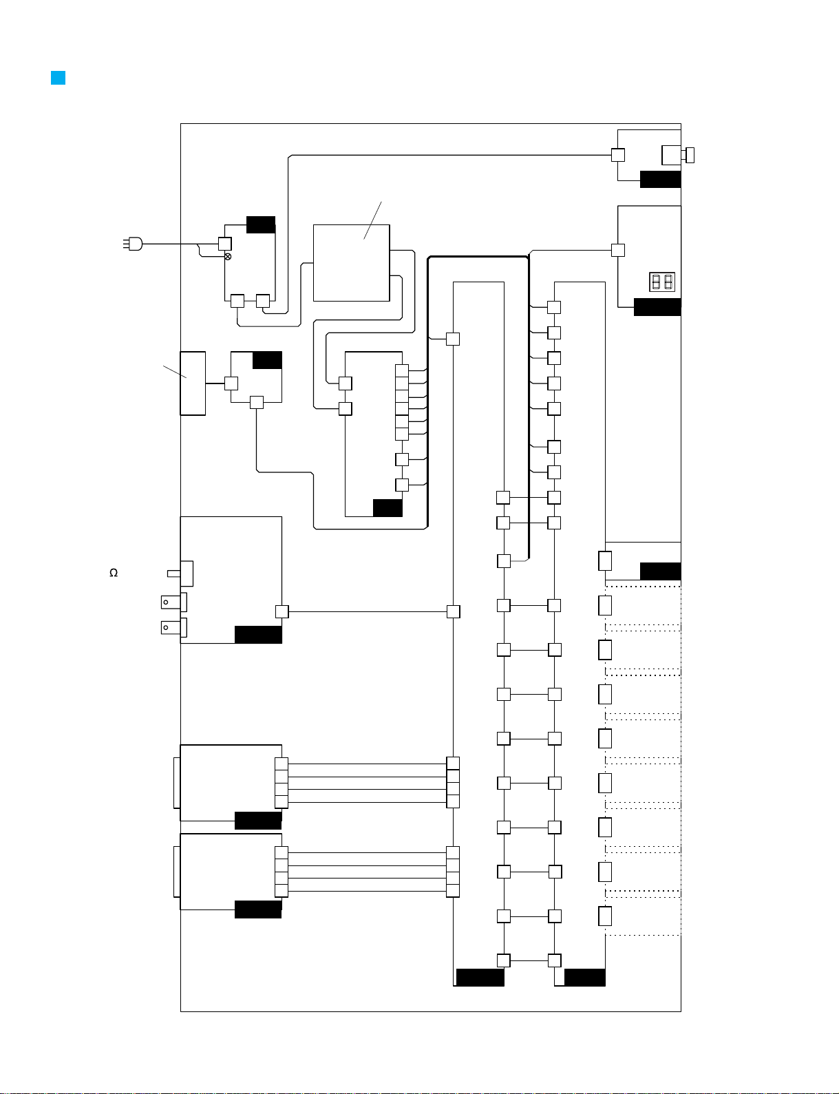
AO8
IFC3
PSB
KEC-92523-2
[POWER
ON/OFF]
3P
CN600
14P
CN100
5P
CN127
**
LED2
[OUTPUT
UNIT ID]
[1]
[2]
[3]
[4]
[5]
[6]
[7]
[8]
SLOT NO.
4P
CN126
4P
CN125
6P
CN124
4P
CN123
6P
CN122
4P
CN121
20P
CN120
30P
CN119
CN109
100P
UNC
CN108
100P
CN107
100P
CN106
100P
CN105
100P
CN104
100P
CN103
100P
CN102
100P
CN101
100P
8P
CN117
8P
CN116
8P
CN115
8P
CN114
8P
CN113
8P
CN112
8P
CN111
8P
CN110
6P
CN118
MB1
POWER
TRANSFORMER
**
6P
CN104
13P
CN605
13P
CN606
10P
CN607
10P
CN608
5P
CN106
20P
CN102
30P
CN101
14P
CN103
8P
CN402
8P
CN403
8P
CN404
8P
CN405
13P
CN601
13P
CN602
10P
CN603
10P
CN604
8P
CN407
8P
CN408
6P
CN105
8P
CN406
8P
CN401
[INPUT]
[A]
[B]
10P
CN104
10P
CN103
13P
CN102
13P
CN101
10P
CN104
10P
CN103
13P
CN102
13P
CN101
3P
CN002
5P
CN001
14P
CN100
4P
CN101
2P
CN300
4P
CN301
2P
CN302
4P
CN303
16P
CN200
6P
CN201
DC
2P
CN400
4P
CN401
3P
CN402
FG
AC
FAN
3P
CN502
2P
CN500
DR
[WORD CLOCK]
[ON]
[OFF]
[75 ]
[IN]
[OUT]
5P
CN300
IPC4
IPC2
IPC2
CONNECTOR CIRCUIT DIAGRAM
4
AO8
5
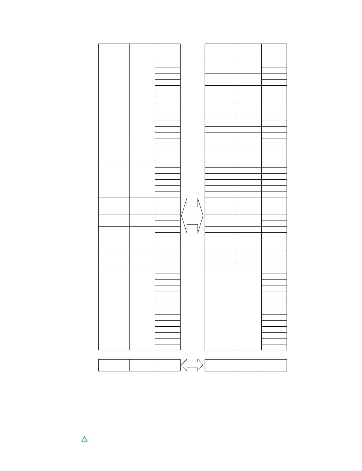
Circuit Board CN No. Pin No.
DC CN100
2
3
4
5
6
7
8
9
10
11
12
13
14
DC CN101 1
2
3
DC CN200
DC CN201
1
2
3
4
5
6
1
2
3
DC CN300 1
2
DC CN301 1
2
3
4
DC CN302 2
DC CN303 1
2
IFC3 CN103 1
2
3
4
5
6
7
8
9
10
11
12
13
14
1 MB1 4
3
MB1 4
3
MB1 5
IFC3 1
2
MB1 2
1
MB1 2
1
MB1
3
IFC3 3
4
MB1 4
IFC3 5
6
4
MB1
MB1
4
MB1 4
MB1 2
MB1 2
MB1 2
DR 1
2
MB1 6
6
MB1 2
1
MB1 1
5
5
LED1 1
2
3
4
5
6
7
8
9
10
11
12
13
14
CN122
CN124
CN127
CN104
CN122
CN124
CN127
CN104
CN127
CN104
CN123
CN121
CN125
CN121
CN123
CN125
CN500
CN122
CN126
CN127
MB1
MB1
CN122
CN124
CN100
CN124
Circuit Board CN No. Pin No.
MB1 1
MB1 1
MB1 1
CN121
CN123
CN125
MB1
AC CN701 1
4
PSB CN600 1
3
KEC-92523-3
1
[1]
[2]
[3]
[4]
[5]
[6]
[7]
Register
Decoder
FLASH RAM
CPU
WC SEL & SYNC DETECTOR
Decoder
Register
DIR2
44.1K
48K
DIR2 2
[8]
Data Bus
Address Bus
SLOT No.
FPGA
MASTER CLOCK
/CS1
/CON1
[75 ]
LOCK
WC
WCI
ID I/O
WCO
INPUT CLOCK
INPUT CLOCK
DIA
WCI
ID I/O
WCO
DIB
[INPUT]
[A]
[B]
[IN]
[OUT]
[WORD CLOCK]
[OUTPUT UNIT ID]
[INPUT SELECTOR]
[A]
[B]
SELECTOR
ATSC
2
O11
O12
O21
O22
O31
O32
O41
O42
O51
O52
O61
O62
O71
O72
O81
O82
/CS2
/CON2
/CS3
/CON3
/CS4
/CON4
/CS5
/CON5
/CS6
/CON6
/CS7
/CON7
/CS8
/CON8
[ON]
[OFF]
WCO
WCI
IC302
IC303
IC202
IC501
IC502
IC404
IC407
IC101
IC201 IC203
IC301
DIR2
IC402
DIR2
IC401
DIR2
IC403
IPC2
Driver
Receiver
IPC2
IPC4
IFC3
Driver
Receiver
KEC-92521
LED2
UNC
MB1
~
ATSC
2
IC502
IC504
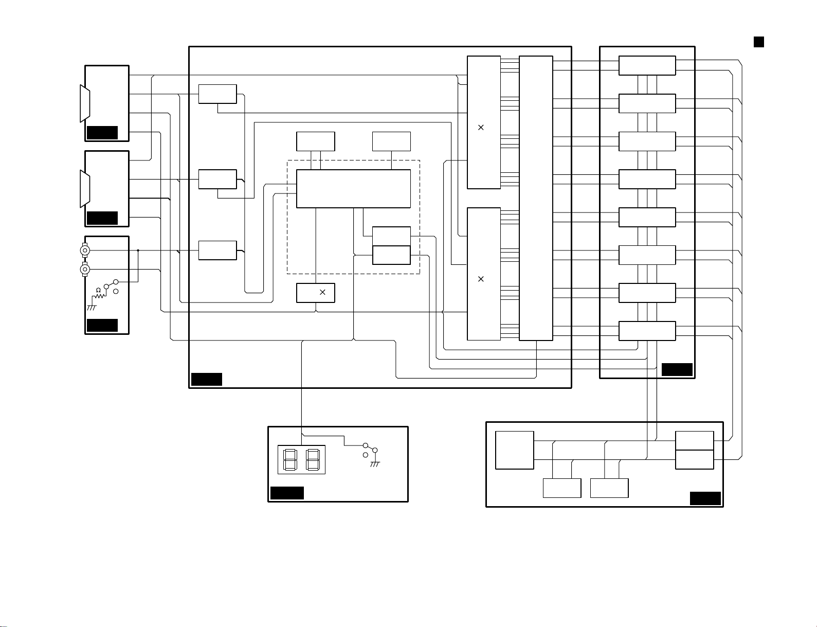
BLOCK DIAGRAM
AO8
6
AO8
7
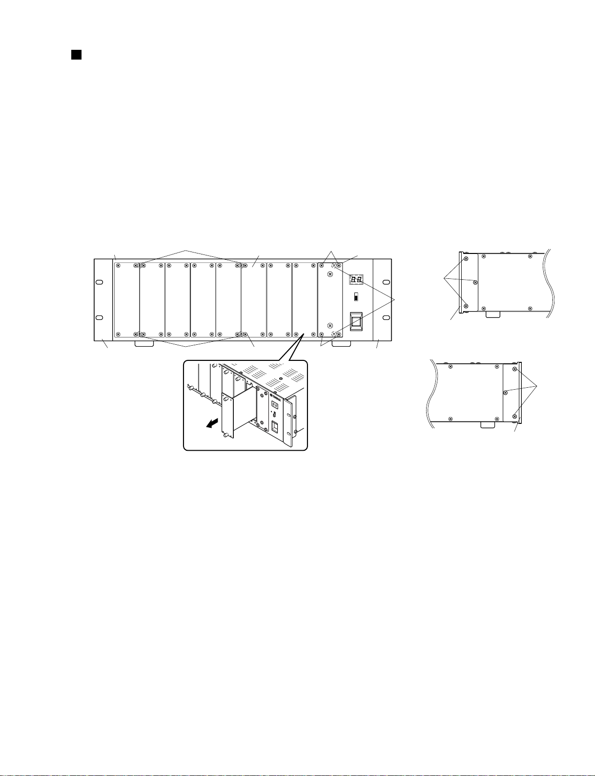
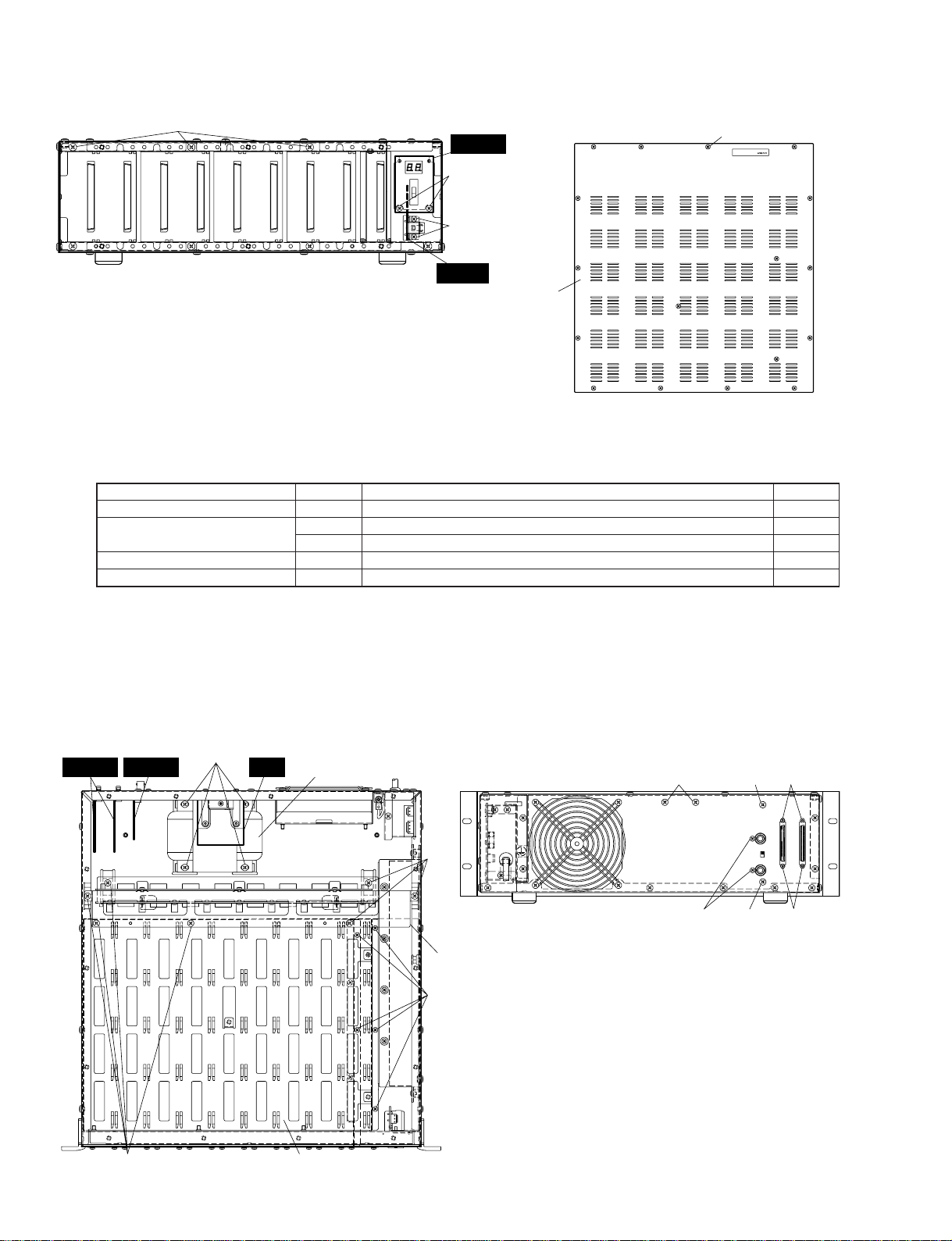
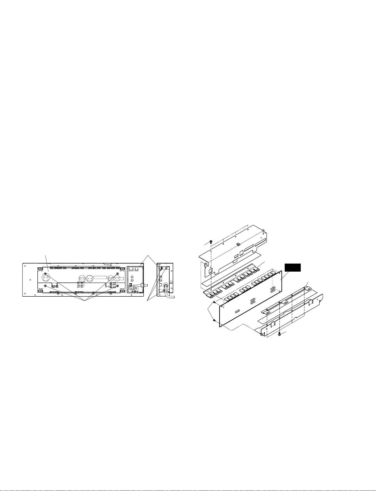
DISASSEMBLY PROCEDURE
3. LED2 Circuit Board
3-1 Remove the front panel assembly. (See Procedure 2.)
3-2 Remove the two (2) screws marked [80]. The LED2
circuit board can then be removed. (Fig. 2)
4. PSB Circuit Board
4-1 Remove the UNC card assembly. (See Procedure 1.)
4-2 Remove the front panel assembly. (See Procedure 2.)
4-3 Remove the seventeen (17) screws marked [430]. The top
panel can then be removed. (Fig. 2)
4-4 Remove the two (2) screws marked [100]. The PSB circuit
board can then be removed. (Fig. 2)
[470]
[500] x 32
[400]: Flat Head Screw 4.0x8 MFZN2BL (VA221200)
[450]: Oval Head Screw 4.0x8 MFZN2BL (VS153600)
[470]: Bonding Screw 3.0x6 MFZN2BL (VS863000)
[500]: Bonding Screw 3.0x6 MFZN2BL (VS863000)
[470]
[400]
[400]
[400]
12345678
[450]
Mount bracket
Mount bracket
Mount bracket
Front panel assembly UNC card assemblyBlank panel
<Right Side View>
<Left Side View>
[450]
Mount bracket
Fig. 1
1. UNC Card Assembly
1-1 Remove the four (4) screws marked [470]. The UNC card
assembly can them be removed. (Fig. 1)
2. Front Panel Assembly
2-1 Remove the UNC card assembly. (See Procedure 1.)
2-2 Remove the thirty-two (32) screws marked [500]. The
blank panel can then be removed. (Fig. 1)
2-3 Remove the six (6) screws marked [450]. Each mount
bracket can then be removed. (Fig. 1)
2-4 Remove the six (6) screws marked [400]. The front panel
assembly can then be removed. (Fig. 1)
[180]: Bind Head Tapping Screw-B A3.0x6 MFZN2BL (VP157900)
[280]: Bind Head Tapping Screw-B A4.0x8 MFZN2BL (VC688800)
Fig. 3
Upper chassis
IPC2 IPC4
[380] [320] [A]
[320][310]
[240]
[280]
[280]
[180]
[A]
Power transformer
Mother assembly
DR
<Top View> <Rear View>
AO8
8
6. Mother Assembly
6-1 Remove the UNC card assembly. (See Procedure 1.)
6-2 Remove the front panel assembly. (See Procedure 2.)
6-3 Remove the top panel. (See Procedure 4-3.)
6-4 Remove the seven (7) screws marked [280]. The mother
assembly can then be removed. (Fig. 3)
5. Circuit Boards and Units
Remove the top panel, each circuit board and unit can
then be removed. (Fig. 3)
[80]: Bind Head Tapping Screw-B 3.0x6 MFZN2BL (EP600230)
[100]: Bind Head Screw 3.0x8 MFZN2BL (VB659000)
[170]: Bind Head Tapping Screw-B A4.0x8 MFZN2BL (VC688800)
[430]: Bind Head Tapping Screw-B A4.0x8 MFZN2BL (VC688800)
Fig. 2
[430] x 17
Top panel
[80]
[170]
[100]
LED2
PSB
<Top View>
Circuit Board and Unit
IPC2
IPC4
DR
Power Transformer
A
310
320
380
240
Screw
Bonding Screw 3.0x6 MFZN2BL (VS863000)
Bind Head Screw A4.0x6 MFZN2BL (EG340290)
Bonding Tapping Screw-B (VN413300)
Bonding Tapping Screw-B (VC688800)
2
2
2
2
4
Ref. No. Screw QTY
[30]: Bind Head Tapping Screw-B 3.0x6 MFZN2BL (EP600230)
[50]: Bind Head Tapping Screw-B 3.0x6 MFZN2BL (EP600230)
[70]: Bind Head Tapping Screw-B 3.0x6 MFZN2BL (EP600230)
Fig. 4
[200]: Bind Head Tapping Screw-B A4.0x8 MFZN2BL (VC688800)
[260]: Bind Head Tapping Screw-B A4.0x8 MFZN2BL (VC688800)
[450]: Oval Head Screw 4.0x8 MFZN2BL (VS153600)
Fig. 5
MB1
[30]
[50]
[70]
[450]
[260]
[260]
Mount bracket Side panel assembly
Side panel L
IFC3
• Mother Assembly <Left Side View>
<Right Side View>
<Rear View>
[450]
[200]
[200]
Mount bracket
AO8
9
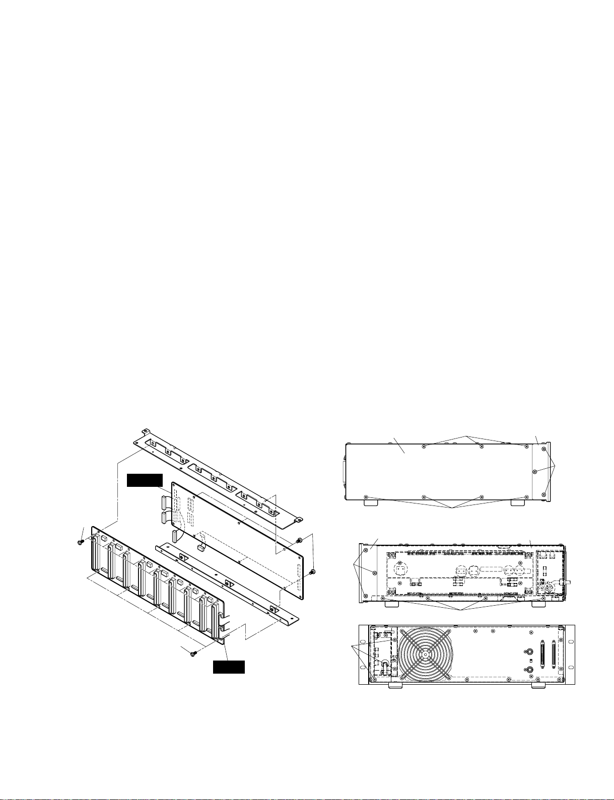
7. MB1 Circuit Board
7-1 Remove the mother assembly. (See Procedure 6.)
7-2 Remove the nine (9) screws marked [30] and the five (5)
screws marked [50]. The MB1 circuit board can then be
removed. (Fig. 4)
8. IFC3 Circuit Board
8-1 Remove the mother assembly. (See Procedure 6.)
8-2 Remove the six (6) screws marked [70]. The IFC3 circuit
board can then be removed. (Fig. 4)
9. Side Panel Assembly
9-1 Remove the UNC card assembly. (See Procedure 1.)
9-2 Remove the front panel assembly. (See Procedure 2.)
9-3 Remove the top panel. (See Procedure 4-3.)
9-4 Remove the mother assembly. (See Procedure 6.)
9-5 Remove the six (6) screws marked [450]. Each mount
bracket can then be removed. (Fig. 5)
9-6 Remove the seven (7) screws marked [200]. The side
panel (L) can then be removed.
9-7 Remove the three (3) screws marked [170] and the five (5)
screws marked [180]. The upper chassis can then be
removed. (Fig. 2, Fig. 3)
9-8 Remove the seven (7) screws marked [260]. The side
panel assembly can then be removed. (Fig. 5)
AO8
10
10. AC Assembly
10-1 Remove the side panel assembly. (See Procedure 9.)
10-2 Remove the three (3) screws marked [90]. The AC
assembly can then be removed. (Fig. 6)
11. DC Assembly
11-1 Remove the side panel assembly. (See Procedure 9.)
11-2 Remove the four (4) screws marked [60]. The DC
assembly can then be removed. (Fig. 6)
12. DC Circuit Board
12-1 Remove the side panel assembly. (See Procedure 9.)
12-2 Remove the DC assembly. (See Procedure 11.)
12-3 Remove the four (4) screws marked [D60]. The TR holder
can then be removed. (Fig. 7)
12-4 Remove the three (3) screws marked [D80]. The BR
holder can then be removed. (Fig. 7)
12-5 Remove the five (5) screws marked [D90]. The DC cricuit
board can then be removed. (Fig. 7)
[60]: Bind Head Screw A4.0x6 MFZN2BL (EG340290)
[90]: Bind Head Tapping Screw-B A4.0x8 MFZN2BL (VC688800)
Fig. 6
[D60]: Pan Head Screw SP4.0x8 MFZN2Y (EL200020)
[D80]: Pan Head Screw SP4.0x8 MFZN2Y (EL200020)
[D90]: Bind Head Tapping Screw-B 3.0x6 MFZN2BL (EP600230)
Fig. 7
[60] [90]
[D60]
DC assembly AC assembly
TR holder
• DC Assembly• Side Panel Assembly
[D80]
[D90]
BR holder
DC
AO8
11
LSI PIN DESCRIPTION
PIN
NO.
I/O FUNCTIONNAME
PIN
NO.
I/O FUNCTIONNAME
1
2
3
4
5
6
7
8
9
10
11
12
13
14
15
16
17
18
19
20
21
22
23
24
25
26
27
28
29
30
31
32
33
34
35
36
37
38
39
40
syncati
mccti
mcbti
VCC
GND
mcati
GND
siat0
siat1
siat2
siat3
ati
GND
ato
soat3
soat2
soat1
soat0
VCC
GND
mcato
GND
mcbto
mccto
syncato
clksel
ato-sel0
ato-sel1
bitsel2
bitsel1
bitsel0
VCC
GND
ext-sync2
ui0
ui1
ui2
ui3
si-sel0
si-sel1
I
I
I
I
I
I
I
I
I
O
O
O
O
O
I
I
I
I
I
I
I
Synch. word input terminal for ati,
siat3-0 input
64 fs clock input terminal for ati,
siat3-0 input
128 fs clock input terminal for ati,
siat3-0 input
Power supply (+5 V)
Ground
256 fs clock input terminal for ati,
siat3-0 input
Ground
Serial data input terminal
Optical input terminal
Ground
Optical output terminal
Serial data output terminal
Power supply (+5 V)
Ground
256 fs clock input terminal for ato,
soat3-0 output
Ground
128 fs clock input terminal for ato,
soat3-0 output
64 fs clock input terminal for ato,
soat3-0 output
Synch. word input terminal for ato,
soat3-0 output
Clock select terminal for ato,
soat 3-0 output
0: mcato,mcbto,mccto,syncato
1: mcai,mcbi,mcci,synci
Format select terminal for ato,
soat3-0 output
Format select terminal for ato,
soat3-0 output
Bit shift select terminal for the ato output
Power supply (+5 V)
Ground
Synch. detect output terminal 2
U-bit input terminal for optical output
input format select terminal for si3-0
input format select terminal for si3-0i
41
42
43
44
45
46
47
48
49
50
51
52
53
54
55
56
57
58
59
60
61
62
63
64
65
66
67
68
69
70
71
72
73
74
75
76
77
78
79
80
synci
mcci
mcbi
VCC
GND
mcai
GND
si0
si1
si2
si3
GND
so3
so2
so1
so0
VCC
GND
mcao
GND
mcbo
mcco
synco
so-sel1
so-sel0
uo3
uo2
uo1
uo0
ext-sync1
VCC
GND
clk
GND
/res
GND
wc-at
mute
ati-sel1
ati-sel0
I
I
I
I
I
I
I
I
O
O
O
O
I
I
I
I
I
I
O
O
O
O
O
I
I
O
I
I
I
Synch. word input terminal for si3-0 input
64 fs clock input terminal for si3-0 input
128 fs clock input terminal for si3-0 input
Power supply (+5 V)
Ground
256 fs clock input terminal for si3-0 input
Ground
Serial data input terminal
Ground
Serial data output terminal
Power supply (+5 V)
Ground
256 fs clock input terminal for so3-0 output
Ground
128 fs clock input terminal for so3-0 output
64 fs clock input terminal for so3-0 output
Synch. word input terminal for so3-0 output
Format select terminal for soat3-0 output
Format select terminal for soat3-0 output
U-bit output terminal for optical output
Synch. detect output terminal 1
Power supply (+5 V)
Ground
Clock input terminal for word clock extract
Ground
System reset input terminal
Ground
Word clock output terminal
Data mute input terminal
Input format select terminal for ati, siat3-0.
input format select terminal for ati, siat3-0.
SGH609080F-47F (XU235A00) ATSC
IFC3: IC501–504
1
1
0
0
so sel1
1
0
1
0
so sel0
not enable to set
so0
so2, 0
so3-0
(8ch/line)
(4ch/line)
(2ch/line)
input format
1
1
0
0
ati sel1
1
0
1
0
ati sel0
ati
ati0
ati2, 0
ati3-0
(8ch/line)
(4ch/line)
(2ch/line)
input format
1
1
0
0
ato sel1
0: mcato,mcbto,mccto,syncato
1: mcai,mcbi,mcci,synci
1
0
1
0
ato sel0
ato
soat0
soat2, 0
soat3-0
(8ch/line)
(4ch/line)
(2ch/line)
output format
1
1
0
0
si sel1
1
0
1
0
si sel0
not enable to set
si0
si2, 0
si3-0
(8ch/line)
(4ch/line)
(2ch/line)
input format
AO8
12
PIN
NO.
I/O FUNCTIONNAME
PIN
NO.
I/O FUNCTIONNAME
1
2
3
4
5
6
7
8
9
10
11
12
13
14
15
16
17
18
19
20
21
22
DAUX
HDLT
DOUT
VFL
OPT
SYNC
MCC
WC
MCB
MCA
SKSY
XI
XO
P256
LOCK
Vss
TC
DIM1
DIM0
DOM1
DOM0
KM1
I
O
O
O
O
O
O
O
O
O
I
I
O
O
O
O
I
I
I
I
I
Auxiliary input for audio data
Asynchronous buffer operation flag
Audio data output
Parity flag output
Fs x 1 Synchronous output signal for DAC
Fs x 1 Synchronous output signal for DSP
Fs x 64 Bit clock output
FS x 1 Word clock output
Fs x 128 Bit clock output
Fs x 256 Bit clock output
Clock synchronization control input
Crystal oscillator connection or external
clock input
Crystal oscillator connection
VCO oscillating clock connection
PLL lock flag
Logic section power (GND)
PLL time constant switching output
Data input mode selection
Data input mode selection
Data output mode selection
Data output mode selection
Clock mode switching input 1
23
24
25
26
27
28
29
30
31
32
33
34
35
36
37
38
39
40
41
42
43
44
RSTN
Vdda
CTLN
PCO
(NC)
CTLP
Vssa
TSTN
KM2
KM0
FS1
FS0
CSM
EXTW
DDIN
LR
Vdd
ERR
EMP
CD0
CCK
CLD
I
I
O
I
I
I
I
O
O
I
I
I
O
O
O
O
I
I
System reset input
VCO section power (+5V)
VCO control input N
PLL phase comparison output
VCO control input P
VCO section power (GND)
Test terminal. Open for normal use
Clock mode switching input 2
Clock mode switching input 0
Channel status sampling frequency
display output 1
Channel status sampling frequency
display output 0
Channel status output method selection
External synchronous auxiliary input
word clock
EIAJ (AES/EBU) data input
PLL word clock output
Logic section power (+5 V)
Data error flag output
Channel status emphasis control code
output
3-wire type microcomputer interface data
output
3-wire type microcomputer interface clock
input
3-wire type microcomputer interface load
input
YM3436DK (XG948E0) DIR2 (Digital Format Interface Receiver)
IFC3: IC301 to 303, 401 to 403
AO8
13
PIN
NO.
I/O FUNCTIONNAME
PIN
NO.
I/O FUNCTIONNAME
1
2
3
4
5
6
7
8
9
10
11
12
13
14
15
16
17
18
19
20
21
22
23
24
25
26
27
28
29
30
31
32
33
34
35
36
37
38
39
40
41
42
43
44
45
46
47
48
49
50
51
52
53
54
55
56
PE14
PE15
VSS
A0
A1
A2
A3
A4
A5
A6
A7
A8
A9
A10
A11
A12
A13
A14
A15
A16
VCC
A17
VSS
/RAS
/CASL
/CASH
VSS
RDWR / PB5
A18
A19
A20
PB9 /A21
VSS
/RD
/WDTOVF
/WRH
VCC
/WRL
VSS
/CS1
/CS0
PA9 / TCLKD
/IRQ2 / TCLKC
/CS3
/CS2
/IRQ1
TXD
RXD
/IRQ0
PA1 / TXD0
PA0 / RXD0
D15
D14
D13
VSS
D12
O
O
I
O
O
O
O
O
O
O
O
O
O
O
O
O
O
O
O
O
I
O
I
O
O
O
O
O
O
O
O
O
I
O
O
O
I
O
I
O
O
O
I
O
O
I
O
I
I
O
I
I/O
I/O
I/O
I
I/O
Port E
Port E
Ground
Address bus
Power supply
Address bus
Ground
Row address strobe
Column address strobe (low)
Column address strobe (high)
Ground
DRAM read/write / Port B
Address bus
Port B / Address bus
Ground
Read
Watch dog timer overflow
High write
Power supply
Low write
Ground
Chip select
Chip select
Port A / Timer clock
Interrupt request / Timer clock
Chip select
Chip select
Interrupt request
Data transmission
Data reception
Interrupt request
Port A / Data transmission
Port A / Data reception
Data bus
Ground
Data bus
57
58
59
60
61
62
63
64
65
66
67
68
69
70
71
72
73
74
75
76
77
78
79
80
81
82
83
84
85
86
87
88
89
90
91
92
93
94
95
96
97
98
99
100
101
102
103
104
105
106
107
108
109
110
111
112
D11
D10
D9
D8
VSS
D7
D6
D5
VCC
D4
D3
D2
D1
D0
VSS
XTAL
MD3
EXTAL
MD2
NMI
VCC
MD1
MD0
PLLVCC
PLLCAP
PLLVSS
PA15 / CK
/RES
PE0
PE1
PE2
PE3
PE4
VSS
AN0 / PF0
AN1 / PF1
AN2 / PF2
AN3 / PF3
AN4 / PF4
AN5 / PF5
AVSS
AN6 / PF6
AN7 / PF7
AVCC
VSS
PE5
VCC
PE6
PE7
PE8
PE9
PE10
VSS
PE11
PE12
PE13
I/O
I/O
I/O
I/O
I
I/O
I/O
I/O
I
I/O
I/O
I/O
I/O
I/O
I
I
I
I
I
I
I
I
I
I
I
I
O
I
I
I
I
I
I
I
I
I
I
I
I
I
I
I
I
I
I
O
I
O
O
O
O
O
I
O
O
O
Data bus
Ground
Data bus
Power supply
Data bus
Ground
Crystal oscillator
Mode control
Crystal oscillator
Mode control
Non-maskable interrupt request
Power supply
Mode control
Mode control
PLL Power supply
PLL capacitor
PLL Ground
Port A / Clock
Reset
Port E
Ground
Analog input / Port F
Analog ground
Analog input / Port F
Analog input / Port F
Power supply
Ground
Port E
Power supply
Port E
Ground
Port E
HD6477042AF28 (XY715A00) CPU UNC: IC101
AO8
14
IC BLOCK DIAGRAM
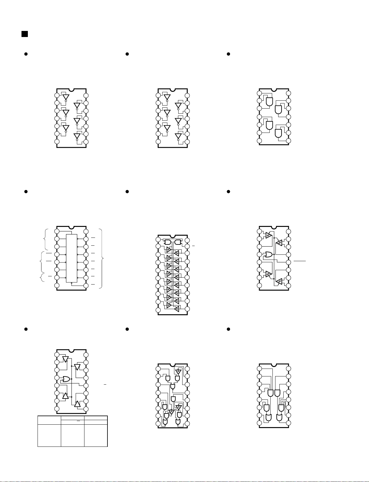
HD74LVU04AFPEL (XY102A00)
Hex Inverter
IFC3: IC105
HD74LV04AFPEL (IS000400)
Hex Inverter
IFC3: IC311, 408
UNC: IC105
HD74LV08AFPEL (IS000800)
Quad 2 Input AND
IFC3: IC104, 310, 409
UNC: IC104, 213
SN74LV138ANSR (IS013810)
3 to 8 Demultiplexer
UNC: IC211, 212
HD74LV245AFPEL (IS024500)
Octal 3-State Bus Transceiver
IPC2: IC104, 105
IFC3: IC101-103, 106, 107, 404-407,
601-608
UNC: IC102, 204, 210
DS26C32ATMX (XU815A00)
Quad Differential Line Receiver
IPC2: IC100-103, 106
AM26LS31CNSR (XU996A00)
Quad Line Driver
IPC2: IC107
SN75124N (XE737A00)
Triple Line Receiver
IPC4: IC300
SN75121 (XE638A00)
Dual Line Driver
IPC4: IC301
1
2
3
4
5
6
7
1A
1Y
2A
2Y
3A
3Y
Vss
14
13
12
11
10
9
8
VDD
6A
6Y
5A
5Y
4A
4Y
1
2
3
4
5
6
7
1A
1Y
2A
2Y
3A
3Y
Vss
14
13
12
11
10
9
8
VDD
6A
6Y
5A
5Y
4A
4Y
1
2
3
1A
1Y
42A
52B
62Y
7
VSS
1B
14
13
12
VDD
4A
11 4Y
10 3B
9 3A
8 3Y
4B
1
2
3
4
5
6
7
A
A
Select
Enable
Output
Output
B
B
C
C
G2A
G2A
G2B
G2B
G1
G1
Y7
Y7 Y5
Y4
Y3
Y2
Y1
Y0
Y6
16
15
14
13
12
11
10
Vcc
YO
Y1
Y2
Y3
Y4
Y5
8
GND
9
Y6
1
2
3
4
5
6
7
20
19
18
17
16
15
14
Vcc
G
B1
B2
B3
B4
B5
B6
B7
B8
8
9
10
12
11
GND
A8
A7
A6
A5
A4
A3
A2
A1
D1R
13
1
2
3
4
5
6
7
INPUT A
INPUT A
OUTPUT A
OUTPUT C
INPUT C
INPUT C
GND
ENABLE
16
15
14
13
12
11
Vcc
INPUT B
INPUT B
OUTPUT B
ENABLE
OUTPUT D
INPUT D
8
9
10
INPUT D
+
-
-
+
+
-
+
1
2
3
4
5
6
7
1A
1Y
1Z
2Z
2Y
2A
GND
ENABLE G
16
15
14
13
12
11
Vcc
4A
4Y
4Z
ENABLE G
3Z
3Y
8
9
10
3A
H= high level
L= low level
X= irrelevant
Z= high impedance (off)
OUTPUTSENABLESINPUT
A
GGYZ
H
H
X
X
L
X
X
L
L
H
H
L
H
L
Z
L
H
L
H
Z
H
L
H
L
X
1A
1B
2R
2S
2A
2B
2Y
GND
1 16
2 15
3 14
4 13
5 12
6 11
7 10
8 9
Vcc
1S
1R
1Y
3A
3S
3R
3Y
Vcc
2F
2E
2A
2Y
GND
1Y
2C
2B
2D
1A
1B
1C
1D
1E
1F
1
2
3
4
5
6
7
8
16
15
14
13
12
11
10
9
3NA-V488240
Component side
INPUT A
INPUT B
IPC2 1/2 Circuit Board
to IFC3-CN602
to IFC3-CN601
to IFC3-CN604
to IFC3-CN603
Component side
to IFC3-CN606
to IFC3-CN605
to IFC3-CN608
to IFC3-CN607
IPC2 2/2 Circuit Board
AO8
15
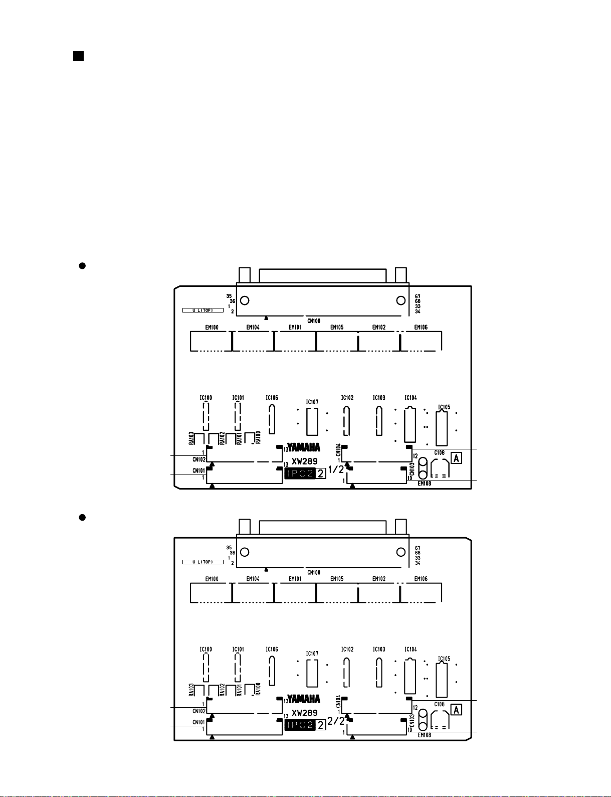
CIRCUIT BOARDS
AC Circuit Board (XW295B0)······················································································· 16
DC Circuit Board (XW295B0)······················································································· 17
DR Circuit Board (XW295B0)······················································································· 16
IFC3 Circuit Board (XW287A0)···················································································· 19
IPC2 Circuit Board (XW289A0)···················································································· 15
IPC4 Circuit Board (XW286B0)···················································································· 16
LED2 Circuit Board (XW286B0)··················································································· 16
MB1 Circuit Board (XW282A0) ···················································································· 17
PSB Circuit Board (XW295B0)····················································································· 16
UNC Circuit Board (XW281B0)···················································································· 18
Note: See parts list for details of circuit board component parts.
 Loading...