


Yamaha AN-200 Service Manual
SERVICE MANUAL
This document is printed on chlorine free (ECF) paper with soy ink.
SY 011548
20010301-59800
CONTENTS
SPECIFICATIONS .............................................................................. 3
PANEL LAYOUT.................................................................................. 4
CIRCUIT BOARD LAYOUT................................................................. 6
WIRING............................................................................................... 6
BLOCK DIAGRAM .............................................................................. 7
DISASSEMBLY PROCEDURE ........................................................... 8
LSI PIN DISCRIPTION.......................................................................11
IC BLOCK DIAGRAM........................................................................ 15
DIMENSIONS ................................................................................... 17
CIRCUIT BOARDS ........................................................................... 18
TEST PROGRAM & INITIALIZE ....................................................... 28
MIDI IMPLEMENTATION CHART..................................................... 40
P ARTS LIST
OVERALL CIRCUIT DIAGRAM
HAMAMATSU, JAPAN
1.494K-059 Y .K Printed in Japan ’01, 02
AN200
IMPORTANT NOTICE
This manual has been provided for the use of authorized Yamaha Retailers and their service personnel. It has been assumed that
basic service procedures inherent to the industry, and more specifically Yamaha Products, are already known and understood by the
users, and have therefore not been restated.
WARNING: Failure to follow appropriate service and safety procedures when servicing this product may result in per-
sonal injury, destruction of expensive components and failure of the product to perform as specified. For
these reasons, we advise all Yamaha product owners that all service required should be performed by an
authorized Yamaha Retailer or the appointed service representative.
IMPORTANT: This presentation or sale of this manual to any individual or firm does not constitute authorization, certifica-
tion, recognition of any applicable technical capabilities, or establish a principal-agent relationship of any
form.
The data provided is believed to be accurate and applicable to the unit(s) indicated on the cover. The research engineering, and
service departments of Yamaha are continually striving to improve Yamaha products. Modifications are, therefor, inevitable and
changes in specification are subject to change without notice or obligation to retrofit. Should any discrepancy appear to exist, please
contact the distributor's Service Division.
WARNING: Static discharges can destroy expensive components. Discharge any static electricity your body may have
accumulated by grounding yourself to the ground bus in the unit (heavy gauge black wires connect to this
bus).
IMPORTANT: Turn the unit OFF during disassembly and parts replacement. Recheck all work before you apply power to
the unit.
WARNING: CHEMICAL CONTENT NOTICE!
The solder used in the production of this product contains LEAD. In addition, other electrical / electronic and / or plastic (where
applicable) components may also contain traces of chemicals found by the California Health and Welfare Agency (and possibly other
entities) to cause cancer and / or birth defects or other reproductive harm.
DO NOT PLACE SOLDER, ELECTRICAL / ELECTRONIC OR PLASTIC COMPONENTS IN YOUR MOUTH FOR ANY REASON
WHAT SO EVER!
Avoid prolonged, unprotected contact between solder and your skin! When soldering, do not inhale solder fumes or expose eyes to
solder / flux vapor!
If you come in contact with solder or components located inside the enclosure of this product, wash your hands before handling food.
LUTHIUM BATTERY HANDLING
This product uses a lithium battery for memory back-up.
WARNING: Lithium batteries are dangerous because they can be exploded by improper handling. Observe the following
●
Leave lithium battery replacement to qualified service personnel.
●
Always replace with batteries of the same type.
●
When installing on the PC board by soldering, solder using the connection terminals provided on the battery cells.
●
Never solder directly to the cells. perform the soldering as quickly as possible.
●
Never reverse the battery polarities when installing.
●
Do not short the batteries.
●
Do not attempt to recharge these batteries.
●
Do not disassemble the batteries.
●
Never heat batteries or throw them into fire.
ADVARSEL!
Lithiumbatteri-Eksplosionsfare ved fejlagtig håndtering. Udskiftning må kun ske med batteri af samme fabrikat og type. Levér
det brugte batteri tilbage til leverandoren.
VARNING
Explosionsfara vid felaktigt batteribyte. Använd samma batterityp eller en ekvivalent typ som rekommenderas av
apparattillverkaren. Kassera använt batteri enlight fabrikantens instruktion.
VAROITUS
Paristo voi räjähtää, jos se on virheellisesti asennettu. Vaihda paristo ainoastaan laitevalmistajan suosittelemaan tyyppiin.
Hävitä käytetty paristo valmistajan ohjeiden mukaisesti.
The following information complies with Dutch Official Gazette 1995. 45; ESSENTIALS OF ORDER ON THE COLLECTION
OF BATTERIES.
● Please refer to the diassembly procedure for the removal of Back-up Battery.
● Leest u voor het verwijderen van de backup batterij deze beschrijving.
precautions when handling or replacing lithium batteries.
2

■SPECIFICATIONS
1.FUNCTIONS
Tone Generator Analog Physical Modeling
2VCO (Osc. Sync, FM), Noise, Ring Mod.,
Filter (FEG), Amp (AEG), 2LFO, PEG + AWM2
Timber 1 (AN) + 3 (AWM2)
Polyphony 5 (AN) + 32 (AWM2) Notes
Effector Distortion, 3-Band EQ (only AN)
+ 1 Effector (Tempo Delay/Reverb,
Flanger/ Chorus, Phaser, Amp.
Simulator)
Pattern Preset Pattern x 256, User Pattern x
128
Scene 2 Scene
Step Sequencer MIDI Sync, MIDI Transmit
Others Free EG (4 tracks)
2.CONTROLLERS
Sound Control Knob x 16
(Cutoff/Filter Type, Resonance, FEG Depth, VCO1/2 Balance,
FM Depth, Sync Pitch, Noise Level, EG Attack, EG Decay,
EG Sustain, EG Release, Portamento Time, Effect Param/
Pan, Effect Wet/Vol, LFO Speed, Scene Control)
Master Volume Knob x 1
Rotary Encorder x 1
3.PANEL SWITCHES
Sound Control Sw. x 8
(LFO Detail, Key Assign, VCO1 Wave, Sync Mode, VCO2
Wave, Effect Type, EG Select, Dist Sw)
Scene x 2, Sequencer. Sw x 2, Mode x 2, Pattern Select x 1,
Keyboard Mode x 1, Step Select x 16, Step Group Select x 2,
Track Select x 2, Play Effect x 2, Octave x 2, Tap Tempo x 1,
Free EG Sw. x 4, Free EG Mode x 1, Free EG Length x 1,
Store x 1, Show Value x 1, Shift x 1, Exit x 1
4.DISPLAY
7SEG LED x 4
5.CONNECTORS
OUTPUT L (MONO)/R Phone x 2
MIDI IN/OUT Din x 2
DC IN
PHONES Stereo phone
6.MAXIMUM OUTPUT LEVEL
Phones +0.5 dBm (33 ohm)
Stereo Output +9.0 dBm (10 kohm)
7.IMPEDANCE
Phones 47Ω
OUTPUT L/R 1kΩ
8.POWER CONSUMPTION
7.4W (DEMO PLAY)
340mA ±10%
9.DIMENSIONS, WEIGHT
338.0 (W) x 208.9 (D) x 51.7 (H) mm, 1600 g
10.ACCESSORIES
CD ROM (for Windows and Macintosh) x 1
Owner's Manual x 1
AC Adaptor x 1
(Power supply recommendation may vary from country to
country. Please check with your nearest Yamaha dealer for
further details.)
AN200
3
AN200
■ PANEL LAYOUT
●
Top Panel
Main block
Voice block
Control block Keyboard block
Main Block
[SONG] button
[PATTERN] button
[DATA] knob
[SHOW VALUE] button
[STORE] button
[EXIT] button
VOICE BLOCK
[SCENE] group
[SCENE] knob
[1] button
[2] button
[FREE EG] group
[LENGTH] button
[1] button
[2] button
[MODE] button
[3] button
[4] button
[VOLUME] knob
[LFO] group
[DETAIL] button
[SPEED] knob
[EG] group
[ATTACK] knob
[DECAY] knob
[SUSTAIN] knob
4

[RELEASE] knob
[SELECT] button
[DIST] group
[SWITCH] button
[COMMON] group
[KEY ASGN] button
[VCO1] group
[WAVE] button
[SYNC] group
[MODE] button
[VCO 2] group
[WAVE] button
[PORTAMENTO] knob
[VCO 1/2] knob
[FM DEPTH] knob
[SYNC PITCH] knob
[NOISE LEVEL] knob
[EFFECT] group
[TYPE] button
[PARAM / PAN] knob
[WET / VOL] knob
[VCF] group
[CUTOFF / TYPE] knob
[RESONANCE] knob
[FEG DEPTH] knob
AN200
CONTROL BLOCK
[씰 / ■] (START / STOP) button
[TAP] button
[●] button
[SWING] button
[REVERSE] button
[SHIFT] button
[OCT <<] button
[OCT >>] button
[KEYBOARD] button
[PATTERN SELECT] button
[SYNTH TRACK] button
[RHYTHM TRACK] button
KEYBOARD BLOCK
●
Rear Panel
DC IN OUTPUT
PHONES
STAND BY / ONMIDI INMIDI OUT
5
AN200
■ CIRCUIT BOARD LAYOUT
■ WIRING
PLG150-AN
LED
DM
DM
PN
CN1(7P)
CN6(4P)CN5(15P)CN2(7P)
CN3(15P)CN4(6P)
CN1(15P)
PLG
LED
28C99-8818208
LOCATION
1
2
3
4
5
6
7
CN1(16P)
1
PN
CONNECTOR NAME
KR-KR
DS-KR
DS-KR
KR-KR
DS-KR
PLG-DM
CN1(16P)
PIN/LENGTH
7
CN3(4P)
16P / L=80
7P / L=450
4P / L=380
15P / L=220
7P / L=150
6P / L=200
15P / L=50
3
CN4(6P)
CN2(15P)
6
PN-CN1
DM-CN2
DM-CN6
DM-CN3
DM-CN1
DM-CN4
DM-CN5
4
DESTINATION
PLG_AN-CN1
LED-CN1
PN-CN5
PN-CN3
PN-CN2
PN-CN6
PN-CN4
CN5(7P)
CN6(7P)
5
2
6
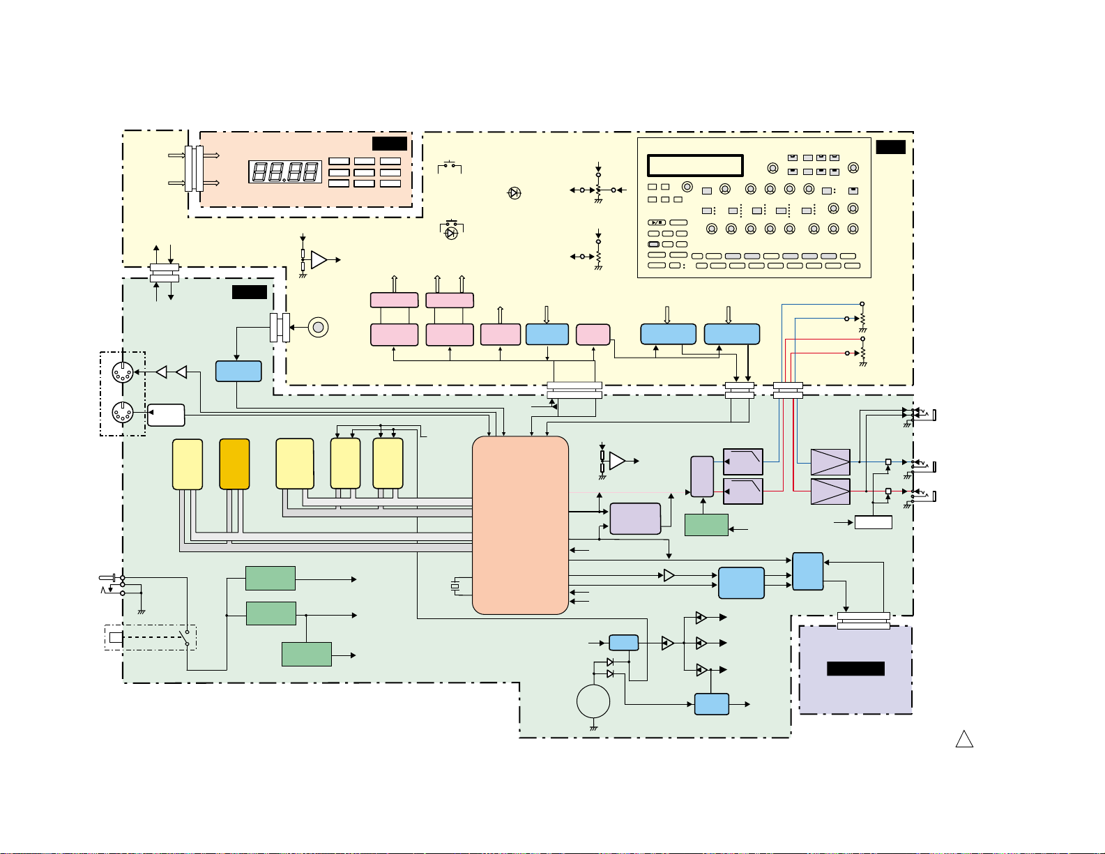
■ BLOCK DIAGRAM
Backup
Battery
3V
RESET
+5V
RES1
RES2
RES3
Analog
Switch
Bat
LED Driver
LED Comon
Latch
to Panel
LED
28CA1-8818204 1
OUTPUT
L/MONO
OUTPUT
R
PHONES
AMP
AMP
Muting
+9V
CN2
DAC
LPF
LPF
+5V
Regurator
STANDBY
ON
MIDI IN
MIDI OUT
DC-DC
Convertor
+3.3V
Regurator
+9V
+5V
+3.3V
CN5
LED Data
Latch
LED Driver
to Panel
LED
SW Data
Buffer
flom Panel
SW
SW Strobe
Latch
to Panel
SW
A/D
Latch
VOLUME
A/D
Multi Plexer
A/D
Multi Plexer
CN6
CN1
flom Knob
VR X 8
flom Knob
VR X 8
CN2
CN3
+1.65V
+3.3V
OP AMP
FLASH
8M
ROM
Program
1M
SRAM
Lower
Buffer
MIDI-A or
MIDI-B
Switch
DC IN
to LED
CN1
1M
SRAM
Upper
flom LED
Driver
CN4
CN4
+5V GND
+5V GND
DATA
CN3CN6
Encoder
I/F
CN1
RES2
CN5
JK4
JK3
JK2
JK1
JK5
RES1
RES3
XTAL
8.4672MHz
Photo
Coupler
C-Bus Control
C-Bus
S-Bus Control
S-Bus
4M
DRAM
DSP
8M
ROM
Wave
+9V
+4.35V
+5V
OP AMP
+5V
WCLK
HCLK
64fs
Synchronous
Divider
+3.3V
Knob out
Knob X 15
+1.65V
+3.3V
Knob out
Knob(center click)
X 1
Panel SW
With LED
X 36
Panel SW
X 15
Panel LED
#A0642=25
Panel Side
CN1
+3.3V
LED
DM
PN
PLG-AN
21 345678
9 10111213141516
TAP
SWING
REVERS
OCT<<OCT
>>
TG
TRACK
SFX
TRACK
KEYBOARD
PATTERN
SELECT
STEP
1~8
STEP
9~16
6P
6P
4P
4P
16P
16P
15P
15P
7P
7P
7P
7P
15P
15P
IC6
IC6
IC11
IC11
IC16
IC19
IC10
IC5
IC5IC5
IC5
IC8
IC26
IC7
IC13,14
IC4
IC20
IC12
IC21 IC22
IC24
IC2
IC3
IC15
IC7 IC8
IC9
IC3 IC2 IC1IC4 IC5, 6
IC25-5,9,13
IC25-4
IC27-3,6
Separate Mode
IC17
SWX00B
79-87,96-99
106-118,121-123
47,48,51-59,62-74
23-34,37-40
9
10
35,119,133,143,161
6,7,12,49,61,77,91
20
130
156,157,159
164
163
158
14,15,16
124,126-128,132
135-142,165
21
154
125,145,152
13,15,16
7
11
6
2
6
1
7
2
6
1
7
7,8,9,14
1,2,5,16
6,11-13,15
18
17
4
7
2,6
1
11 8
IC4
711101312
12
98
3
1
4
2
1
3
1
4
1
3
1,3
4,6
31
3,4,7,8,17,18 3,4,7,8,17,18
2,5,6,9,
12,15,16
2,5,6,9,
12,15,16
11-18
2-9
1,3,4,
7,8
2,5,6,
9,12
6,9,11 3
1,2,4,5,
12-15
6,9,11 3
1,2,4,5,
12-15
6543
D13
D12
1
+9V
Regurator
AN200
7
AN200
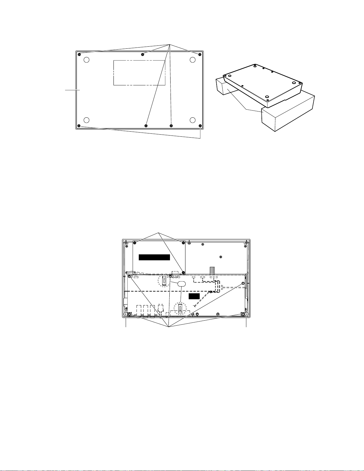
■ DISASSEMBLY PROCEDURE
Bottom Assembly
[180]
AN200
Bottom side
Wooden bolster
(Fig. 1)
[180]: Bind Head Tapping Screw-B 3.0X6 MFZN2Y (EP600130)
[185]: Bind Head Tapping Screw-B 3.0X6 MFZN2Y (EP600130)
1.
Bottom Assembly (time required: about 1 min)
1-1 Remove the five (5) screws marked [180] and the
two (2) screws marked [185]. The bottom assembly
can then be removed. (Fig. 1)
* If you turn the mixer upside down for disassem-
bling and assembling, put 2 wooden bolsters
underneath the unit at its both side ends to protect
the PN circuit board from being damaged.
[160]
(Fig. 1-1)
PLG150-AN
[185]
*1
*1
DM
(Fig. 1-1)
[120]: Bind Head Tapping Screw-P 2.6X8 MFZN2Y (EP620100)
[130]: Angle, L (V655450)
[140]: Angle, R (V655460)
[160]: Bind Head Tapping Screw-B 3.0X86 MFZN2Y (EP620130)
2. PLG150-AN Circuit Board (time required: about 1 min)
2-1 Remove the bottom assembly. (See Procedure 1.)
2-1 Remove the tree (3) screws marked [160]. The
PLG150-AN circuit board can then be removed. (Fig. 2)
*
Attachment consideration of the PLG150-AN circuit board.
When installing the PLG150-AN circuit board, do
with connector assembly as shown in the fig 2-1.
Fit the PLG150-AN circuit board caring not to let
the connector assembly in it.
8
(Fig. 2)
[120][130] [140]
3.
DM Circuit Board (time required: about 2 min)
3-1 Remove the bottom assembly. (See Procedure 1.)
3-2
Remove the PLG150-AN circuit Board. (See Procedure 2.)
3-3 Remove the six (6) screws marked [120]. The DM
circuit board can then be removed. (Fig. 2)
* Attachment consideration of the DM circuit board
Confirm that the DM contact terminal [110b],
which is on the backside of the DM circuit board,
is not distorted or bent. Contact it appropriately on
the bottom board assembly. Replace any terminal
when it is bent or broken. (Fig. 2-2)
DM
AN200
CN5
DM-PLG
Connector Assembly
CN1
PLG150-AN
(Fig. 2-1)
[210] [200]
SONG
PATTERN STORE
VELOCITYGATE TIMEPITCH
INST SEL BPM BEAT
DM Terminal
orOK
NG
(Fig. 2-2)
[100b]: DM Terminal (V7450500)
[60][60]
PN
[200]
(Fig. 3)
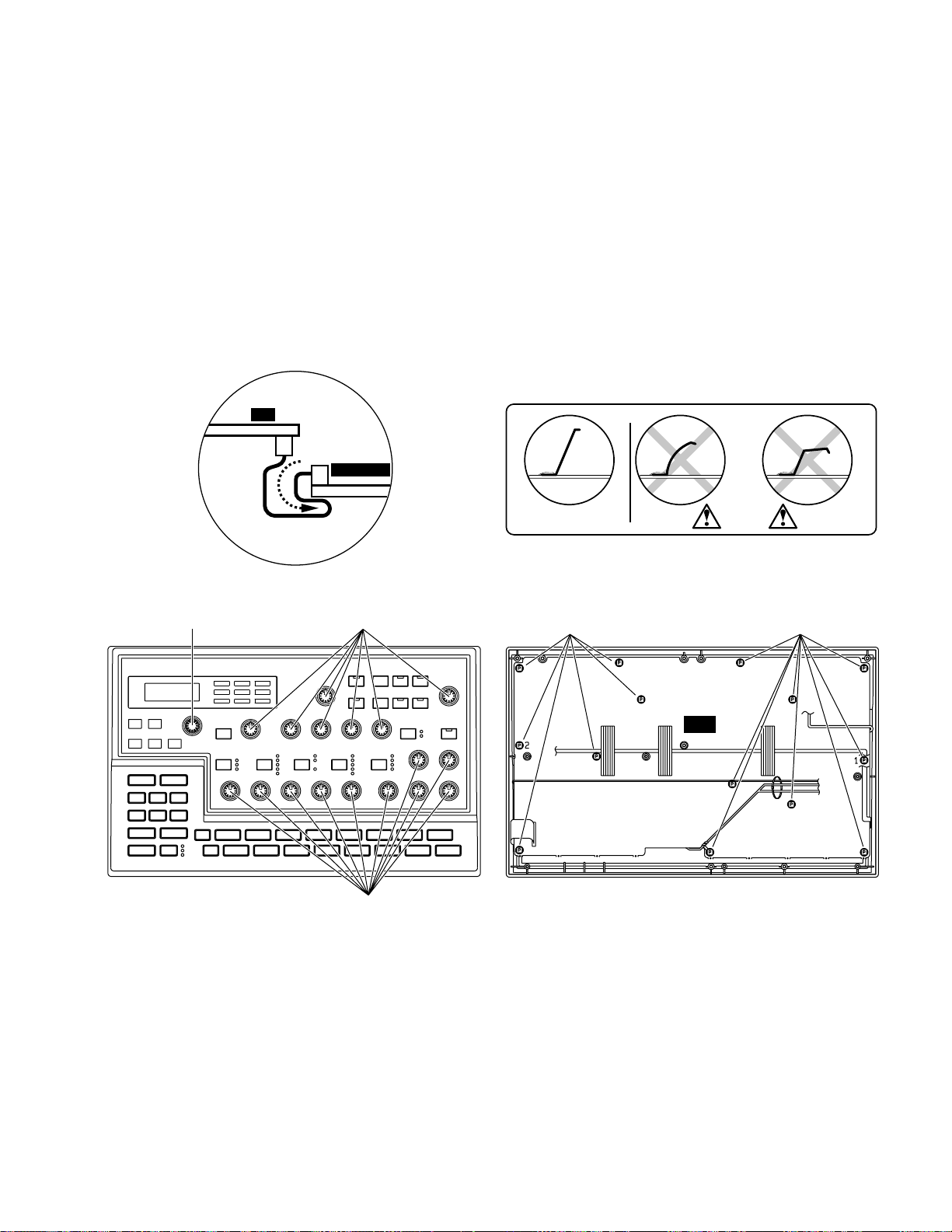
[200]: Knob K-CB (V4765800)
[210]: Knob (VU931600)
4.
PN Circuit Board (time required: about 4 min)
[60]: Bind Head Tapping Screw-P 2.6X8 MFZN2Y (EP620100)
4-1 Remove the bottom assembly. (See Procedure 1.)
4-2
Remove the PLG150-AN circuit Board. (See Procedure 2.)
4-3 Remove the DM circuit Board. (See Procedure 3.)
4-4 Remove the seventeen (17) knobs marked [200]
and one (1) knob marked [210]. (Fig. 3)
4-5 Remove the fourteen (14) screws marked [60]. The
PN circuit board can then be removed. (Fig .4)
(Fig. 4)
9
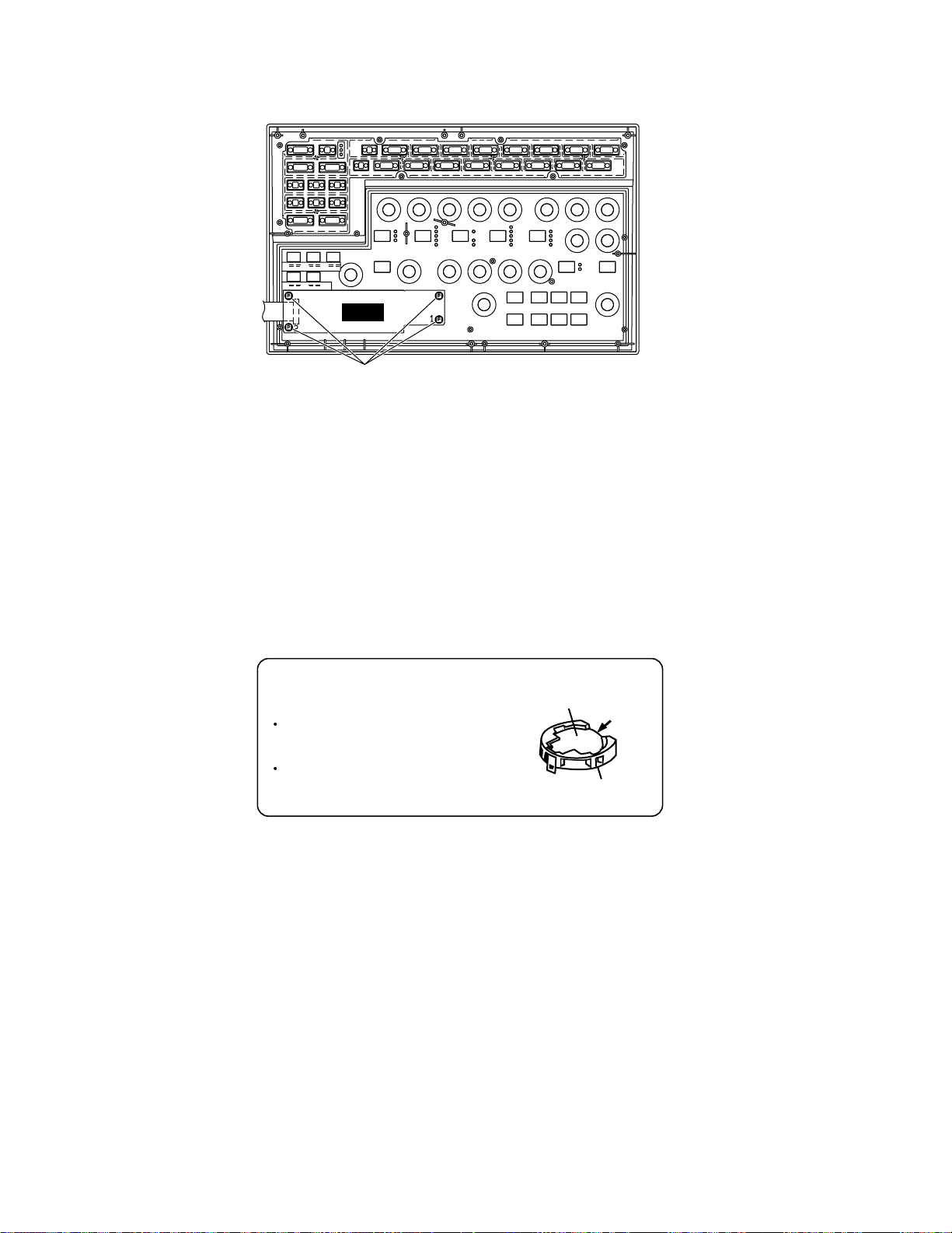
AN200
LED
[40]
[40]: Bind Head Tapping Screw-P 2.6X8 MFZN2Y (EP620100)
5.
LED Circuit Board (time required: about 5 min)
5-1 Remove the bottom assembly. (See Procedure 1.)
5-2
Remove the PLG150-AN circuit Board. (See Procedure 2.)
5-3 Remove the DM circuit Board. (See Procedure 3.)
5-4 Remove the PN circuit Board. (See Procedure 4.)
5-5 Remove the four (4) screws marked [40]. The LED
circuit board can then be removed. (Fig. 5)
(Fig. 5)
Battery VN103500
VN103600 (Battery holder for VN103500)
Notice for back-up battery removal
push the battery as shown in figure,
then the battery will pop up.
Druk de batterij neer beneden zoals
aangeven in de tekening, de batterij
springt dan neer voren.
Battery
Battery holder
10
■ LSI PIN DISCRIPTION
●
HG73C205AFD (XU947C00) SWX00B TONE GENERATOR DM: IC17
PIN
NAME I/O FUNCTION
NO. NO.
1
10
11
12
13
14
15
16
17
18
19
20
21
22
23
24
25
26
27
28
29
30
31
32
33
34
35
36
37
38
39
40
41
42
43
44
45
46
47
48
49
50
51
52
53
54
55
56
57
58
59
60
61
62
63
64
65
66
67
68
69
70
71
72
73
74
75
76
77
78
79
80
81
82
83
84
2
3
4
5
6
7
8
9
ICN
RFCLKI
TM2
AVDD_PLL
AVSS_PLL
MODE0
VCC7
GND8
XIN
XOUT
MODE1
TEST0
TESTON
AN0-P40
AN1-P41
AN2-P42
AN3-P43
AVDD_AN
AVSS_AN
TXD0
TXD1
EXCLK
SMD11
SMD4
SMD3
SMD12
SMD10
SMD5
SMD2
SMD13
SMD9
SMD6
SMD1
SMD14
VCC35
GND36
SMD8
SMD7
SMD0
SMD15
SOE
SWE
SRAS
SCAS
REFRESH
CS0
SMA0
SMA16
VCC49
GND50
SMA1
SMA15
SMA2
SMA14
SMA3
SMA13
SMA4
SMA12
SMA5
GND60
VCC61
SMA11
SMA6
SMA10
SMA7
SMA9
SMA17
SMA8
SMA18
SMA19
SMA20
SMA21
SMA22
SMA23
CMA20
CMA19
VCC77
GND78
CMA18
CMA17
CMA5
CMA6
CMA4
CMA7
I
Initial clear
I
PLL Clock
I
PLL Control
Power supply
Ground
I
SWX dual mode
Power supply
Ground
I
crystal oscillator
O
crystal oscillator
I
SWX separate mode
I
TEST pin
I
TEST pin
I
I
A/D converter
I
I
Power supply
Ground
O
for MIDI or TO-HOST
O
for MIDI
I
Crystal oscillator
I/O
I/O
I/O
I/O
I/O
I/O
Wave memory data bus
I/O
I/O
I/O
I/O
I/O
I/O
Power supply
Ground
I/O
I/O
Wave memory data bus
I/O
I/O
O
read signal
O
write signal
O
RAS signal
O
CAS signal
O
REFRESH signal
O
CS signal
O
Memory address bus
O
Power supply
Ground
O
O
O
O
O
Memory address bus
O
O
O
O
Ground
Power supply
O
O
O
O
O
O
O
Memory address bus
O
O
O
O
O
O
O
Program address bus
O
Power supply
O
Ground
O
O
O
Program address bus
O
O
O
PIN
NAME I/O FUNCTION
85
86
87
88
89
90
91
92
93
94
95
96
97
98
99
100
101
102
103
104
105
106
107
108
109
110
111
112
113
114
115
116
117
118
119
120
121
122
123
124
125
126
127
128
129
130
131
132
133
134
135
136
137
138
139
140
141
142
143
144
145
146
147
148
149
150
151
152
153
154
155
156
157
158
159
160
161
162
163
164
165
166
167
168
CMA3
CMA8
CMA2
CRD
CMA1
CUB
VCC91
GHND92
CS1
CMA0
CLB
CMA12
CMA11
CMA10
CMA9
GND100
CWE
CMA16
CMA15
CMA14
CMA13
CMD8
CMD7
CMD9
CMD6
CMD10
CMD5
CMD11
CMD4
CMD12
CMD3
CMD13
CMD2
CMD14
VCC119
GND115
CMD1
CMD15
CMD0
CMA21
PDT15
PDT14
PDT13
PDT12
PDT11
PDT10
PDT9
PDT8
VCC133
GND134
PDT7
PDT6
PDT5
PDT4
PDT3
PDT2
PDT1
PDT0
VCA143
GND144
PAD2
PAD1
PAD0
VCC148
GND149
PCS
PWR
PRD
RXD0
RXD1
SCLKI
ADIN
ADLR
DO0
DO1
SYSCLK
VCC161
GND162
WCLK
QCLK
BCLK
SYI
IRQ0
NMI
I/O
I/O
I/O
I/O
I/O
I/O
I/O
I/O
I/O
I/O
I/O
I/O
I/O
I/O
I/O
I/O
I/O
I/O
I/O
I/O
I/O
I/O
I/O
I/O
I/O
I/O
I/O
I/O
I/O
I/O
I/O
I/O
O
O
O
O
O
O
O
O
O
O
O
O
O
O
O
O
O
O
O
I
I
I
I
I
I
I
I
I
I
O
O
O
O
O
O
O
I
I
I
Program address bus
read signal
Program address bus
high byte effective signal
Power supply
Ground
CS signal
Program address bus
low byte effective signal
Program address bus
Ground
write signal
Program address bus
Program memory Data bus
Power supply
Ground
Program memory Data bus
Program address bus
SWX access data bus
Power supply
Ground
SWX access data bus
Power supply
Ground
SWX access address bus
Power supply
Ground
Chip select
write enable
read enable
for Midi or TO-HOST
for Midi or Key scan
EXT Clock
A/D converter
A/D converter LR clock
DAC
1/2 clock
Power supply
Ground
for DAC LR clock
1/12 clock
IIS-DAC clock
Synch signal
Interrupt request
AN200
11
AN200
●
YSS236-F (XT013A00) VOP3 PLG150-AN: IC4
PIN
NAME I/O FUNCTION
NO. NO.
1
10
11
12
13
14
15
16
17
18
19
20
21
22
23
24
25
26
27
28
29
30
31
32
33
34
35
36
37
38
39
40
41
42
43
44
45
46
47
48
49
50
51
52
53
54
55
56
57
58
59
60
61
62
63
64
65
66
67
68
69
70
71
72
73
74
75
76
77
78
79
80
VSS
2
WA17
3
WA16
4
WA15
5
WA14
6
WA13
7
WA12
8
WA11
9
WA10
VDD
VSS
WA09
WA08
WA07
WA06
WA05
WA04
WA03
WA02
VDD
VSS
WA01
WA00
WEN
OEN
RASN
CASN
CEN
VDD
VSS
WD19
WD18
WD17
WD16
WD15
WD14
VDD
VSS
WD13
WD12
WD11
WD10
WD09
WD08
WD07
VDD
VSS
WD06
WD05
WD04
WD03
WD02
WD01
WD00
VDD
VSS
TST2
TST1
TST0
MS
LRCLK
SI7
SI6
VDD
VSS
SI5
SI4
SI3
SI2
SI1
SI0
DB1
DB0
VDD
VSS
ODFM
OFS3
OFS2
OFS1
OFS0
Power supply
O
O
O
O
External memory address bus
O
O
O
O
Ground
Power supply
O
O
O
O
External memory address bus
O
O
O
O
Ground
Power supply
O
External memory address bus
O
O
External memory control (WEN)
O
External memory control (OEN)
O
External memory control (RASN)
O
External memory control (CASN)
O
External memory control (CEN)
Ground
Power supply
I/O
I/O
I/O
External memory data bus
I/O
I/O
I/O
Ground
Power supply
I/O
I/O
I/O
I/O
External memory data bus
I/O
I/O
I/O
Ground
Power supply
I/O
I/O
I/O
I/O
External memory data bus
I/O
I/O
I/O
Ground
Power supply
O
O
Test output
O
I
Memory select
O
LR clock for ADC
I
OSerial input
I
Ground
Power supply
I
I
I
Serial input
I
I
I
I
Output bit type select for DAC
I
Ground
Power supply
I
Output mode select for DAC
I
I
Serial output format select
I
I
PIN
NAME I/O FUNCTION
81
82
83
84
85
86
87
88
89
90
91
92
93
94
95
96
97
98
99
100
101
102
103
104
105
106
107
108
109
110
111
112
113
114
115
116
117
118
119
120
121
122
123
124
125
126
127
128
129
130
131
132
133
134
135
136
137
138
139
140
141
142
143
144
145
146
147
148
149
150
151
152
153
154
155
156
157
158
159
160
SO7
SO6
SO5
VDD
VSS
SO4
SO3
SO2
SO1
SO0
WDCK
SWPKON
IRQN
VDD
VSS
XTAL_I
XTAL_O
MCLK
VDD
VSS
MICN
CLKIN
SYWIN
SYW
SYWD
VDD
VSS
CLKO
WCLK
HCLK
QCLK
TSTCI
VDD
VSS
(NC)
VDD(PLL)
CPO
CPIN
REF
VSS(PLL)
(NC)
VDD
VSS
TSTCS
CA6
CA5
CA4
CA3
CA2
VDD
VSS
CA1
CA0
CSN
RDN
WRN
BTYP
VDD
VSS
CD15
CD14
CD13
CD12
CD11
VDD
VSS
CD10
CD09
CD08
CD07
CD06
CD05
VDD
VSS
CD04
CD03
CD02
CD01
CD00
VDD
I/O
I/O
I/O
I/O
I/O
I/O
I/O
I/O
I/O
I/O
I/O
I/O
I/O
I/O
I/O
I/O
O
O
O
O
O
O
O
O
O
O
O
I
O
O
I
I
I
O
O
O
O
O
O
I
O
I
I
I
I
I
I
I
I
I
I
I
I
I
Serial output
Ground
Power supply
Serial output
Data enable for DAC
SWP00 format key on output
EG interrupt
Ground
Power supply
Quartz crystal terminal
Quartz crystal terminal
Oscillate clock output
Ground
Power supply
Initial clear
Master clock input
Sync.signal input
Sync.signal output
Sync.signal output
Ground
Power supply
For test (512 fs output)
2 times sync.clock output (256fs)
4 times sync.clock output (128fs)
8 times sync.clock output (64fs)
PLL test input
Ground
Power supply
PLL control output
PLL control input
PLL control intput
Ground
Power supply
PLL test input
CPU address bus
Ground
Power supply
CPU address bus
Lo/Hi select in 8 bits write
Chip select
Register read
Register write
Data bus type select
Ground
Power supply
CPU data bus
Ground
Power supply
CPU data bus
Ground
Power supply
CPU data bus
Ground
12
●
HD6413002FP16 (XQ375A00) CPU PLG150-AN: IC1
PIN
NAME I/O FUNCTION
NO. NO.
1
2
3
VCC
4
5
6
7
8
9
10
PB6//DREQ0
11
PB7//DREQ1
12
/RESO
13
14
P90/TXD0
15
P91/TXD1
16
P92/RXD0
17
P93/RXD1
18
P94/SCK0
19
P95/SCK1
20
P40/D0
21
P41/D1
22
P42/D2
23
P43/D3
24
25
P44/D4
26
P45/D5
27
P46/D6
28
P47/D7
29
30
31
32
33
34
35
36
37
VCC
38
39
40
41
42
43
44
45
46
47
48
49
50
PA6
PA7
PB0
PB1
PB2
PB3
PB4
PB5
VSS
VSS
D8
D9
D10
D11
D12
D13
D14
D15
A0
A1
A2
A3
A4
A5
A6
A7
VSS
A8
A9
A10
A11
O
Port A
O
Address bus
Power supply
I
I
I
I
Port B
I
I
I
I
O
Reset
Ground
O
Transmit data (MIDI OUT)
O
KSN-ACK
I
Receive data (MIDI IN)
I
KSN-RX
O
Port 9
I
Port 9
I/O
I/O
I/O
I/O
Ground
I/O
I/O
I/O
I/O
Data bus
I/O
I/O
I/O
I/O
I/O
I/O
I/O
I/O
Power supply
O
O
O
O
O
O
O
Address bus
O
Ground
O
O
O
O
PIN
NAME I/O FUNCTION
51
52
53
54
55
56
57
58
59
60
61
62
63
64
65
66
67
68
69
70
71
72
73
74
75
76
77
78
79
80
81
82
83
84
85
86
87
88
89
90
91
92
93
94
95
96
97
98
99
100
A12
A13
A14
A15
A16
A17
A18
A19
VSS
P60//WAIT
P61//BREQ
P62//BACK
/STBY
/RES
NMI
VSS
EXTAL
XTAL
VCC
/AS
/RD
/HWR
/LWR
MD0
MD1
MD2
AVCC
VREF
P70/AN0
P71/AN1
P72/AN2
P73/AN3
P74/AN4
P75/AN5
P76/AN6
P77/AN7
AVSS
P80
P81//CS3
P82//CS2
P83//CS1
P84//CS0
VSS
PA0
PA1
PA2
PA3
PA4
PA5
O
O
O
O
O
O
O
O
I
I
I
O
O
I
I
I
I
O
O
O
O
O
I
I
I
I
I
I
I
I
I
I
I
I
O
O
O
O
O
I
I
I
O
O
O
Address bus
Ground
Port 6
Oout
Stand-by mode signal
Reset
Non-maskable interrupt
Ground
Clock
Clock
Power supply
Address strobe
Read strobe
Write strobe (High)
Write strobe (Low)
Mode select
Analog power supply
Reference voltage
Analog data input (EQ)
Analog input (EQ)
Analog data input
Analog input (CS)
Analog data input (BEND)
Analog input (MOD)
Analog input (FC)
Analog input (BAT)
Analog ground
Port 8
Chip select
Ground
Port A
AN200
13

AN200
●
UPD63200GS-E1 (XP867A00) DAC (Digital to Analog Converter) DM: IC16
PIN
NAME I/O FUNCTION
NO. NO.
1
2
3
4
5
6
7
8
4/8F
D. GND
16 BIT
D. VDD
A. GND
R. OUT
A. VDD
A. VDD
I
4/8 Fs selection
Digital ground
I
16 bit/18 bit selection
Digital power supply
Analog ground
O
Channel R output
Analog power supply
PIN
NAME I/O FUNCTION
9
R. REF
10
L. REF
L. OUT
12
13
14
15
16
11
A. GND
WDCK
RSI
SI/LSI
CLK
O
I
I
I
I
Channel R voltage reference
Channel L voltage reference
Channel L output
Analog ground
Word clock
Channel R series input
Series input/Channel L series input
Clock
14
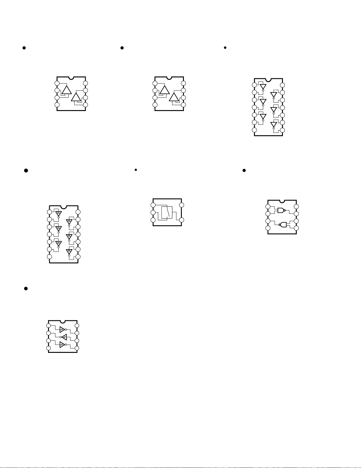
■ IC BLOCK DIAGRAM
AN200
SN74HC157NSR
MM74HC157SJX
(XW110A00)
(XY310A00)
Quad 2 to 1 Multiplexer
DM: IC7
1
SELECT
2
1A 1A
3
1B 1B
4
1Y 1Y
5
2A 2A
6
2B 2B
7
2Y 2Y
8
GND
TC74HC245AF (XS720A00)
HD74HC245FPV (XV611A00)
MM74HC245ASJX (XW107A00)
TC74VHC245FT (XU797A00)
HD74LV245AT (XW744A00)
TRANSCEIVER
1D1R
2
A1
3
A2
A3
4
5
A4
6
A5
A6
7
A7
8
A8
9
GND
10
16
S3 Y
Vcc
15
STROBEG
14
4A
4A
13
4B4B
12
4Y4Y
11
3A3A
10
3B3B
9
3Y
DM:
IC26
PLG150-AN: IC13
PN:IC3
CC
V
20
G
19
B1
18
B2
17
B3
16
B4
15
B5
14
B6
13
B7
12
B8
11
MM74HC74ASJX
HD744C74FPEL
TC74HC74AF EL
(XY153A00)
(XL096A00)
(XW890A00)
Dual D-Type Flip-Flop
DM: IC14
1
1CLR
2
D
1D
3
1CK
4
1PR
GND
PR CLR CLK D Q Q
L
H
L
H
H
H
PR
5
Q
1Q
6
Q
1Q
7
INPUTS OUTPUTS
X
H
X
L
X
L
f
H
f
H
L
H
HD74HC273FP(XU533A00
14
VCC
13
CLR
CK
X
X
X
H
L
X
2CLR
D
12
CLR
2D
11
CK
2CK
10
2PR
PR
9
Q
2Q
8
Q
2Q
L
H
H
L
H
H
L
H
H
L
O
O
Q
Q
)
MM74HC273SJX(XY198A00)
D-FF
PN: IC1,IC2,IC4,IC5,IC6
V
CC
20
8Q
19
8D
18
7D
17
CK
DCK
CL
7Q
16
6Q
15
CK
D
6D
14
5D
13
CK
CL
Q
5Q
12
11
CLOCK
GND
1CLEAR
1Q
2
1D
3
2D
4
2Q
5
3Q
6
3D
7
4D
8
4Q
9
10
QQ
CL CL
CK CK
DD
D
CL
QQ
QQ
CL CL
CK
D
DDCK
CL
Q
IC25
HD74HC4051FPEL (XP373A00)
TC74HC4051AFEL (XY549A00)
Triple 2-Ch.Multiplexer/Demultiplexer
Swtches IN/OUT Y1
Swtches IN/OUT Y0
Swtches IN/OUT Z1
Commons OUT/IN Z0
Swtches IN/OUT Z0
Control Inhibit
-DC Voltage Supply
GND
1
2
3
4
5
6
7
8
16
+DC Voltage Supply
15
Commons OUT/IN Y
14
Commons OUT/IN X
13
Switches IN/OUT X1
12
Switches IN/OUT X0
11
Control IN/OUT A
10
Control IN/OUT B
Control IN/OUT B
9
PN: IC7,IC8
TC74VHC153FT (XV894A00)
Dual 4 to 1 Data Selectors
PLG150-AN: IC8
STROBE B
1C3
1C2
1C1
1C0
GND
1
2
1G
3
4
5
BB
6
B
A
A
1Y
7
8 9
Vcc
161G SELECT
SELECT 2G
15
STROBE A
14
2G
2C3
13
2C2
12
2C1
11
B
A
A
2C0
10
OUTPUT
2Y
2Y
TC74VHC139FT (XV893A00)
Dual 2-to-4 Line Decoder/Demultiplexers
PLG150-AN: IC14
Vcc
16
2G
15
2A
14
2B
13
2Y0
12
2Y1
11
2Y2
10
2Y3
9
1Y0
1Y1
1Y2
1Y3
GND
1
1G
2
1A
3
1B
4
5
6
7
8
NJM4556AMT1 (XQ138A00)
M5216FP-600C
(XP263A00)
µPC4570G2 (XF291A00)
Dual Operational Amplifier
DM: IC6,IC18
+-
8
7
6
5
+DC Voltage
Supply
Output B
Inverting
Input B
Non-Inverting
Input B
Output A +V
Inverting
Input A
Non-Inverting
Input A
-DC Voltage Supply
1
2
3
4-V
+-
15
AN200
TC7W00FU
Dual 2-input Nand Gate
1
2
3
4
8
7
6
5
(XV189A00)
1A
1B
2Y
GND 2A
2B
1Y
Vcc
DM: IC13
NJM4580E-T1
(XQ781A00)
Dual Operational Amplifier
DM: IC11
+DC Voltage
+-
+-
8
7
6
5
Supply
Output B
Inverting
Input B
Non-Inverting
Input B
Output A V
Inverting
Input A
Non-Inverting
Input A
-DC Voltage Supply
1
2
3
4-
MM74HC14JX(XW104A00)
TC74VHC14FT (XV890A00)
Hex Inverter
DM: IC5
PLG150-AN: IC9
GND
11A
1Y
2
3
2A
4
2Y
5
3A
6
3Y
7
DD
V
14
6A
13
6Y
12
5A
11
5Y
10
4A
9
4Y
8
NJM3414AM-T1
(XR294A00)
Dual Operational Amplifier
PN: IC9
+DC Voltage
+-
+-
8
Supply
7
Output B
Inverting
6
Input B
Non-Inverting
5
Input B
Output A V
1
Inverting
2
Input A
Non-Inverting
-DC Voltage Supply
3
Input A
4-
TC7S66F (XR682A00)
TC74HCT04AF-T1 (XI297A00)
Hex Inverter
DM: IC4
1
1A
2
1Y
3
2A
4
2Y
5
3A
6
3Y
7
Vss
14
VDD
13
6A
12
6Y
11
5A
10
5Y
9
4A
8
4Y
Bilateral Switch
DM: IC8
OUT / IN
GND
1IN / OUT
2
3
CC
V
5
CONT
4
TC7W14FU (XN883A00)
Schmitt Inverter
1A
1
3Y
2
2A
3
GND
4
16
DM: IC27
8
Vcc
7
1Y
6
3A
5
2Y
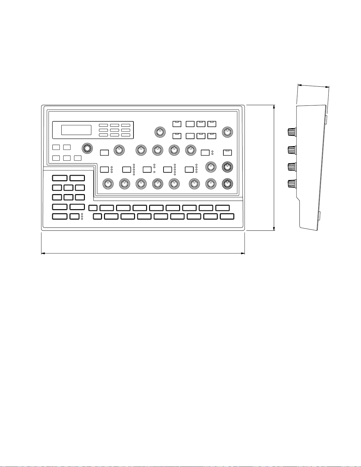
■ DIMENSIONS
338 mm (W)
208.9 mm (D)
51.7 mm (H)
SONG
PITCH
INST SEL
PATTERN
GATE TIME
BPM
STORE
VELOCITY
BEAT
AN200
17
AN200
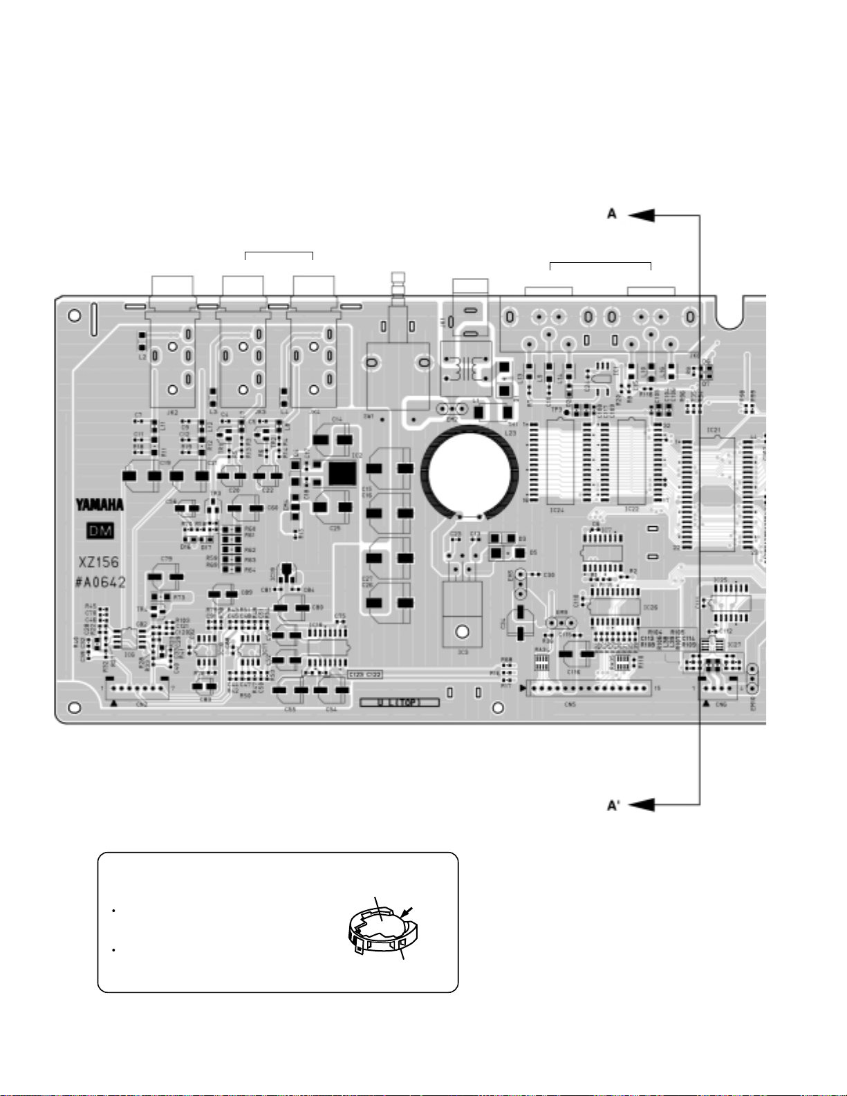
■ CIRSUIT BOARDS
●
DM CIRCUIT BOARD
PHONES
L/MONO
OUTPUT
STAND BY
R
ON
DC IN
IN OUT
MIDI
18
to PN CN5
Battery VN103500
VN103600 (Battery holder for VN103500)
Notice for back-up battery removal
push the battery as shown in figure,
then the battery will pop up.
Druk de batterij neer beneden zoals
aangeven in de tekening, de batterij
springt dan neer voren.
to PLG150-AN CN1 to PN CN3
Battery
Battery holder