

Page 1
查询XC95144XV供应商
0
R
DS051 (v2.2) August 27, 2001
01
Features
• 144 macrocells with 3,200 usable gates
• Available in small footprint packages
- 100-pin TQFP (81 user I/O pins)
- 144-pin TQFP (117 user I/O pins)
- 144-pin CSP (117 user I/O pins)
• Optimized for high-perfo rmance 2.5V systems
- Low power operation
- Multi-voltage operation
• Advanced syste m features
- In-system programmable
- Two separate output banks
- Superior pin-locking and routability with
FastCONNECT II™ switch matrix
- Extra wide 54-input Function Blocks
- Up to 90 product-terms per macrocell with
individual product-term allocation
- Local clock inversion with three global and one
product-term clocks
- Individual output enable per output pin
- Input hysteresis on all user and boundary-scan pin
inputs
- Bus-hold ciruitry on all user pin inputs
- Full IEEE Standard 1149.1 boundary-scan (JTAG)
• Fast concurrent programming
• Slew rate control on individual outputs
• Enhanced data security features
• Excellent quality and reliability
- Endurance exceeding 10,000 program/erase
cycles
- 20 year data retention
- ESD protection exceeding 2,000V
Description
The XC95144XV is a 2.5V CPLD targeted for high-performance, low-voltage applications in leading-edge communications and computing systems. It is comprised of eight
54V18 Function Blocks, providing 3,200 usable gates with
propagation delays of 4 ns.
XC95144XV High-Performance
CPLD
Advance Product Specification
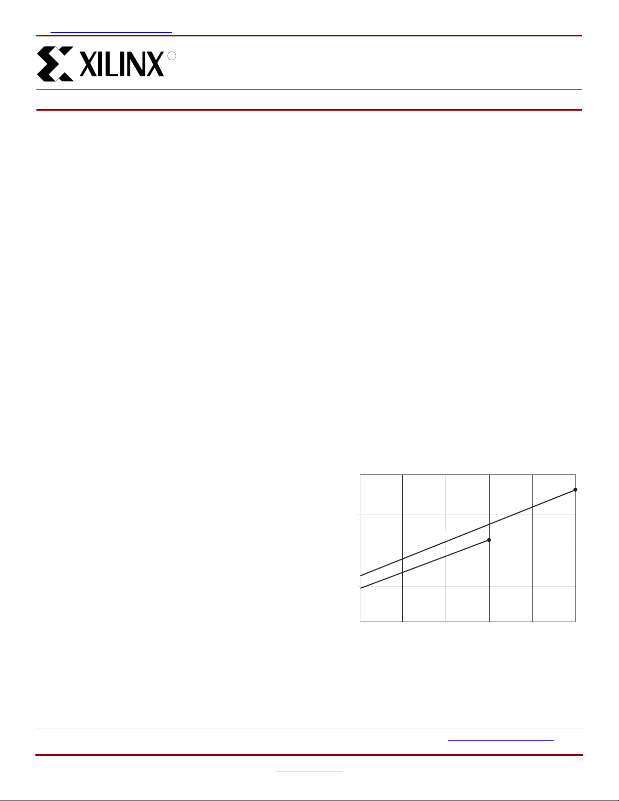
Power Estimation
Power dissipation in CPLDs can vary substantially depending on the system frequency, design application and output
loading. To help reduce power dissipation, each macrocell
in a XC9500XV device may be configured for low-power
mode (from the default high-performance mode). In ad dition, unused product-terms and macrocells are automatically deactivated by the software to further conserve power.
For a general estimate of I
used:
(mA ) =
I
CC
(0.36) + MCLP(0.23) + MC(0.005 mA/MHz) f
MC
HP
Where:
MC
= Macrocells in high-performance (default) mode
HP
MC
= Macrocells in low-power mode
LP
MC = Total number of macrocells used
f = Clock frequency (MHz)
This calculation is based on typical operating conditions
using a pattern of 16-bit up/down counters in each Function
Block with no output loading. The actual I
with the design application and should be verified during
normal system operation.
Figure 1 shows the above estimation in a graphical form.
200
150
(mA)
100
CC
High Performanc
w
o
Typical I
50
0120200
L
Figure 1: Typical ICC vs. Frequency for XC95144XV
, the following equation may be
CC
CC
120 MHz
e
ower
P
Clock Frequency (MHz)
value varies
200 MHz
16040 80
DS051_01_012501
© 2001 Xilinx, Inc. All rights reserved. All Xilinx trademarks, registered trademarks, patents, and disclaimers are as listed at http://www.xilinx.com/legal.htm.
All other trademarks and registered trademarks are the property of their respective owners. All specifications are subject to change without notice.
DS051 (v2.2) August 27, 2001 www.xilinx.com 1
Advance Product Specificati on 1-800-255-7778
Page 2
XC95144XV High-Performance CPLD
R
JTAG Port
I/O/GCK
I/O/GSR
I/O/GTS
I/O
I/O
I/O
I/O
I/O
I/O
I/O
I/O
3
1
JTAG
Controller
In-System Programming Controller
54
18
Function
Block 1
Macrocells
1 to 18
54
18
Function
Block 2
Macrocells
I/O
1 to 18
Blocks
54
18
Function
Block 3
Macrocells
FastCONNECT II Switch Matrix
1 to 18
3
1
18
4
54
Function
Block 4
Macrocells
1 to 18
54
18
Function
Block 8
Macrocells
1 to 18
DS051_02_041000
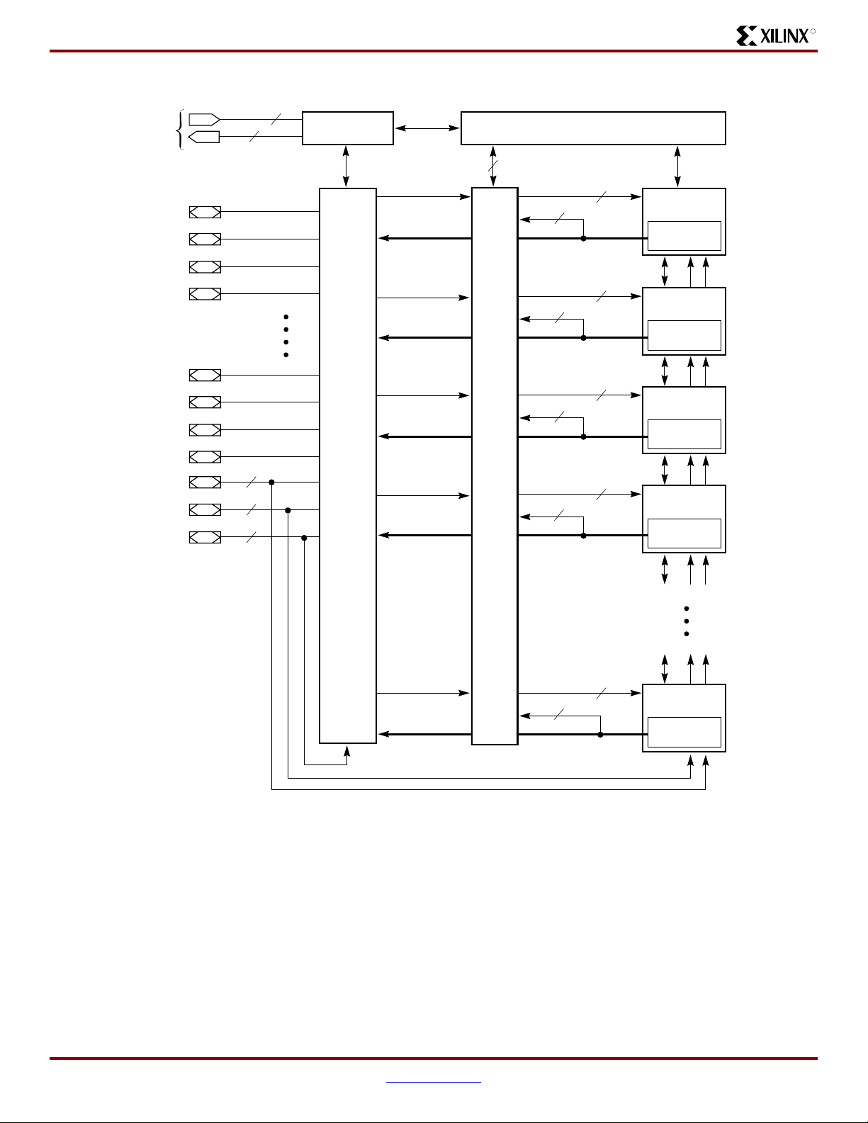
Figure 2: XC95144XV Architecture
Function Block outputs (indicated by the bold line) drive the I/O Blocks directly.
2 www.xilinx.com DS051 (v2.2) August 27, 2001
1-800-255-7778 Advance Product Specification
Page 3
R
XC95144XV High-Performance CPLD
Absolute Maximum Ratings
Symbol Description Value Units
V
CC
V
CCIO
V
IN
V
TS
T
STG
T
SOL
T
J
Notes:
1. Maximum DC unders hoot bel ow GND must be l imit ed to ei ther 0. 5V or 10 m A, whi chever is easi er to a chie v e . Durin g tra nsitions , the
device pins may undershoot to –2.0V or overshoot to +3.6V, provided this over- or undershoot lasts less than 10 ns and with the
forcing current being limited to 200 mA.
2. Stresses beyond those listed under Absolute Maximum Ratings may cause permanent damage to the device. These are stress
ratings onl y, and functional operation of t he device at these or any other condit ions beyond those list ed under Operating Conditions
is not implied. Exposure to Absolute Maximum Ratings conditions for extended periods of time may affect device reliab ility.
Supply voltage relative to GND –0.5 to 2.7 V
Supply voltage for output drivers –0.5 to 3.6 V
Input voltage relative to GND
Voltage applied to 3-state output
Storage temperature (ambient) –65 to +150
Maximum soldering temperature (10s @ 1/16 in. = 1.5 mm) +260
Junction temperature +150
(1)
(1)
–0.5 to 3.6 V
–0.5 to 3.6 V
o
o
o
C
C
C
Recommended Operation Conditions
Symbol Parameter Min Max Units
V
CCINT
V
CCIO
Supply voltage for internal logic
and input buffers
Supply voltage for output drivers for 3.3V operation 3.13 3.46 V
Supply voltage for output drivers for 2.5V operation 2.37 2.62 V
Commercial TA = 0oC to +70oC2.372.62 V
Industrial T
= –40oC to +85oC2.372.62
A
Supply voltage for output drivers for 1.8V operation 1.71 1.89 V
V
IL
V
IH
V
O
Low-level input volt ag e 0 0.8 V
High-level input voltage 1.7 3.6 V
Output voltage 0 V
CCIO
Quality and Reliability Characteristics
Symbol Parameter Min Max Units
V
T
N
ESD
DR
PE
Data retention 20 - Years
Program/Erase cycles (endurance) 10,000 - Cycles
Electrostatic Discharge (ESD) 2,000 - Volts
V
DS051 (v2.2) August 27, 2001 www.xilinx.com 3
Advance Product Specificati on 1-800-255-7778
Page 4

XC95144XV High-Performance CPLD
DC Characteristics (Over Recommended Operating Conditions)
Symbol Parameter Test Conditions Min Max Units
R
V
OH
Output high voltage for 3.3V outputs IOH = –4.0 mA 2.4 - V
Output high voltage for 2.5V outputs I
Output high voltage for 1.8V outputs I
V
OL
Output low voltage for 3.3V outputs IOL = 8.0 mA - 0.4 V
Output low voltage for 2.5V outputs I
Output low voltage for 1.8V outputs I
C
I
I
I
CC
IL
IH
IN
Input leakage low current VCC = 2.62V
Input leakage high current VCC = 2.62V
I/O capacitance VIN = GND
Operating Supply Current
(low power mode, active)
AC Characteristics
XC95144XV-4 XC95144XV-5 XC95144XV-7
Symbol Parameter
T
PD
T
SU
T
H
T
CO
f
SYSTEM
T
PSU
T
PH
T
PCO
T
OE
T
OD
T
POE
T
POD
T
AO
T
PAO
T
WLH
T
PLH
Notes:
1.
Please c on t ac t X ilin x for up- t o- da te informati o n o n a dvan c e specificat ions.
I/O to output valid - 4.0 - 5.0 - 7.5 ns
I/O setup time before GCK 2.8 - 3.5 - 4.8 - ns
I/O hold time after GCK 0 - 0 - 0 - ns
GCK to output valid - 2.8 - 3.5 - 4.5 ns
Multiple FB internal operating
- 250.0 - 222.2 - 125.0 MHz
frequency
I/O setup time before p-term clock
0.8 - 1.0 - 1.6 - ns
input
I/O hold time after p-term clock input 2.0 - 2.5 - 3.2 - ns
P-term clock output valid - 4.8 - 6.0 - 7.7 ns
GTS to output valid - 3.2 - 4.0 - 5.0 ns
GTS to output disable - 3.2 - 4.0 - 5.0 ns
Product term OE to output enabled - 5.6 - 7.0 - 9.5 ns
Product term OE to output disabled - 5.6 - 7.0 - 9.5 ns
GSR to output valid - 7.9 - 10.0 - 12.0 ns
P-term S/R to output valid - 8.5 - 10.7 - 12.6 ns
GCK pulse width (High or Low) 2.0 - 2.2 - 4.0 - ns
P-term clock pulse width (High or Low) 5.0 - 5.0 - 6.5 - ns
Advance Information Preliminary Information
= –1.0 mA 2. 0 - V
OH
= –100 µA 90% V
OH
= 1.0 mA - 0.4 V
OL
= 100 µA-0.4V
OL
CCIO
-V
-10µA
V
= 3.6V
CCIO
V
= GND or 3.6V
IN
-10µA
V
= 3.6V
CCIO
V
= GND or 3.6V
IN
-10pF
f = 1.0 MHz
VI = GND, No load
29 mA
f = 1.0 MHz
UnitsMin Max Min Max Min Max
4 www.xilinx.com DS051 (v2.2) August 27, 2001
1-800-255-7778 Advance Product Specification
Page 5

R
V
TEST
R
Device Output
1
R
2
C
L
Output Type V
V
CCIO
3.3V
2.5V
1.8V
Figure 3: AC Load Circuit
Internal Timing Parameters
XC95144XV-4 XC95144XV-5 XC95144XV-7
Symbol Parameter
Buffer Delays
T
IN
T
GCK
T
GSR
T
GTS
T
OUT
T
EN
Product Term Control Delays
T
PTCK
T
PTSR
T
PTTS
Internal Register and Combinatorial Delays
T
PDI
T
SUI
T
HI
T
ECSU
T
ECHO
T
COI
T
AOI
T
RAI
T
LOGI
T
LOGILP
Feedback Delays
T
F
Time Adders
T
PTA
T
PTA2
T
SLEW
Notes:
1.
Please c on t ac t X ilin x for up- t o- da te informati o n o n a dvan c e specificat ions.
Input buffer delay - 1.6 - 2.0 - 2.3 ns
GCK buffer delay - 1.0 - 1.2 - 1.5 ns
GSR buffer delay - 1.6 - 2.0 - 3.1 ns
GTS buffer delay - 3.2 - 4.0 - 5.0 ns
Output buffer delay - 1.6 - 2.1 - 2.5 ns
Output buffer enable/disable delay - 0 - 0 - 0 ns
Product term clock delay - 1.4 - 1.7 - 2.4 ns
Product term set/reset delay - 0.6 - 0.7 - 1.4 ns
Product term 3-state delay - 4.0 - 5.0 - 7.2 ns
Combinatorial logic propagation delay - 0.2 - 0.2 - 1.3 ns
Register setup time 1.6 - 2.0 - 2.6 - ns
Register hold time 1.2 - 1.5 - 2.2 - ns
Register clock enable setup time 1.6 - 2.0 - 2.6 - ns
Register clock enable hold time 1.2 - 1.5 - 2.2 - ns
Register clock to output valid time - 0.2 - 0.2 - 0.5 ns
Register async. S/R to output delay - 4.7 - 5.9 - 6.4 ns
Register async. S/R recover before clock 4.0 5.0 7.5 ns
Internal logic delay - 0.6 - 0.7 - 1.4 ns
Internal low power logic delay - 5.6 - 5.7 - 6.4 ns
FastCONNECT II™ feedback delay - 1.6 - 1.6 - 3.5 ns
Incremental product term allocator delay - 0.6 - 0. 7 - 0. 8 ns
Adjacent macrocell p-term allocator delay - 0.2 - 0.3 - 0.3 ns
Slew-rate limited delay - 3.0 - 3.0 - 4.0 ns
Advance Information Preliminary Information
XC95144XV High-Performance CPLD
TEST
3.3V
2.5V
1.8V
R
1
320Ω
250Ω
10KΩ
R
2
360Ω
660Ω
14KΩ
DS051_03_0601000
C
L
35 pF
35 pF
35 pF
UnitsMin Max Min Max Min Max
DS051 (v2.2) August 27, 2001 www.xilinx.com 5
Advance Product Specificati on 1-800-255-7778
Page 6

XC95144XV High-Performance CPLD
XC95144XV I/O Pins
R
Function
Block
Macro-
cell
TQ100 TQ144 CS144
BScan
Order Bank
Function
Block
Macro-
cell
TQ100 TQ144 CS144
BScan
Order Bank
1 1 - 23 H3 429 1 3 1 - 39 M3 321 1
1 2 11 16 F1 426 1 3 2 23
(1)
32
(1)
L1
(1)
318 1
1 3 12 17 G2 423 1 3 3 - 41 K4 315 1
1 4 - 25 J1 420 1 3 4 - 44 N4 312 1
1 5 13 19 G3 417 1 3 5 24 33 L2 309 1
1 6 14 20 G4 414 1 3 6 25 34 L3 306 1
1 7 - --411- 3 7 - 46 L5 303 1
1 8 15 21 H1 408 1 3 8 27
(1)
38
(1)
N2
(1)
300 1
1 9 16 22 H2 405 1 3 9 28 40 N3 297 1
1 10 - 31 K3 402 1 3 10 - 48 N5 294 1
1 11 17 24 H4 399 1 3 11 29 43 M4 291 1
1 12 18 26 J2 396 1 3 12 30 45 K5 288 1
1 13 ---393- 3 13 - - - 285 1 14 19 27 J3 390 1 3 14 32 49 K6 282 1
1 15 20 28 J4 387 1 3 15 33 50 L6 279 1
1 16 - 35 M1 384 1 3 16 - - - 276 1 17 22
118
(1)
--- 378 - 3 18 - - - 270 -
30
(1)
K2
(1)
381 1 3 17 34 51 M6 273 1
2 1 - 142 C3 375 2 4 1 - 118 C9 267 2
2 2 99
(1)
143
(1)
A2
(1)
372 2 4 2 87 126 A7 264 2
2 3 - --369- 4 3 - 133 A5 261 2
2 4 - 4C13662 4 4 - - - 258 2 5 1
2 6 2
(1)
(1)
(1)
2
(1)
3
B1
C2
(1)
363 2 4 5 89 128 D7 255 2
(1)
360 2 4 6 90 129 A6 252 2
2 7 - --357- 4 7 - - - 249 2 8 3
2 9 4
(1)
(1)
(1)
5
(1)
6
D4
D3
(1)
354 2 4 8 91 130 B6 246 2
(1)
351 2 4 9 92 131 C6 243 2
2 10 - 7D23482 4 10 - 135 C5 240 2
2 11 6 9E43452 4 11 93 132 D6 237 2
2 12 7 10 E3 342 2 4 12 94 134 B5 234 2
2 13 - 12 E1 339 2 4 13 - 137 A4 231 2
2 14 8 11 E2 336 2 4 14 95 136 D5 228 2
2 15 9 13 F4 333 2 4 15 96 138 B 4 225 2
2 16 - 14 F3 330 2 4 16 - 139 C4 222 2
2 17 10 15 F2 327 2 4 17 97 140 A3 219 2
218---324-
Notes:
1. Global contro l pi n.
4 18 - - - 216 -
6 www.xilinx.com DS051 (v2.2) August 27, 2001
1-800-255-7778 Advance Product Specification
Page 7

R
XC95144XV High-Performance CPLD
Function
Block
Macro-
cell
TQ100 TQ144 CS144
BScan
Order Bank
Function
Block
Macro-
cell
TQ100 TQ144 CS144
BScan
Order Bank
5 1 - --213- 7 1 - --1055 2 35 52 N6 210 1 7 2 50 71 N12 102 1
5 3 - 59 L8 207 1 7 3 - 75 L12 99 1
5 4 - --204- 7 4 - --965 5 36 53 M7 201 1 7 5 52 74 M13 93 1
5 6 37 54 N7 198 1 7 6 53 76 L13 90 1
5 7 - 66 M10 195 1 7 7 - 77 K10 87 1
5 8 39 56 K7 1 92 1 7 8 54 78 K11 84 1
5 9 40 57 N8 189 1 7 9 55 80 K13 81 1
5 10 - 68 N11 186 1 7 10 - 79 K12 78 1
5 11 41 58 M8 183 1 7 11 56 82 J11 75 1
5 12 42 60 K8 180 1 7 12 58 85 H10 72 1
5 13 - 70 L11 177 1 7 13 - 81 J10 69 1
5 14 43 61 N9 174 1 7 14 59 86 H11 66 1
5 15 46 64 K9 171 1 7 15 60 87 H12 63 1
5 16 - --168- 7 16 - 83 J12 60 1
5 17 49 69 M11 1 65 1 7 17 61 88 H13 57 1
5 18- - -162- 7 18- - -546 1 - --159- 8 1 - --516 2 74 106 C11 156 2 8 2 63 91 G11 48 2
6 3 - --153- 8 3 - 95 F11 45 2
6 4 - 111 B11 150 2 8 4 - 97 E13 42 2
6 5 76 110 A12 147 2 8 5 64 92 G10 39 2
6 6 77 112 A11 144 2 8 6 65 93 F13 36 2
6 7 - --141- 8 7 - --336 8 78 113 D10 138 2 8 8 66 94 F12 30 2
6 9 79 116 A10 135 2 8 9 67 96 F10 27 2
6 10 - 115 B10 132 2 8 10 - 101 D13 24 2
6 11 80 119 B9 129 2 8 11 68 98 E12 21 2
6 12 81 120 A9 126 2 8 12 70 100 E10 18 2
6 13 - --123- 8 13 - 103 D11 15 2
6 14 82 121 D8 120 2 8 14 71 102 D12 12 2
6 15 85 124 A8 117 2 8 15 72 104 C13 9 2
6 16 - 117 D9 114 2 8 16 - 107 B13 6 2
6 17 86 125 B7 111 2 8 17 73 105 C12 3 2
6 18- - -108- 8 18- - - 0-
DS051 (v2.2) August 27, 2001 www.xilinx.com 7
Advance Product Specificati on 1-800-255-7778
Page 8
XC95144XV High-Performance CPLD
XC95144XV Global, JTAG and Power Pins
Pin Type TQ100 TQ144 CS144
I/O/GCK1 22 30 K2
I/O/GCK2 23 32 L1
I/O/GCK3 27 38 N2
I/O/GTS1 3 5 D4
I/O/GTS2 4 6 D3
I/O/GTS3 1 2 B1
I/O/GTS4 2 3 C2
I/O/GSR 99 143 A2
TCK 48 67 L10
TDI4563L9
TDO 83 122 C8
TMS 47 65 N10
R
V
2.5V 5, 57, 98 8, 42, 84, 141 B3, D1, J13, L4
CCINT
V
CCIO
1
V
CCIO
2
GND 21, 31, 44, 62, 69, 75, 84,
26, 38, 51 37, 55, 73 L7, N1, N13
88 1, 109, 127 A1, A13, C7
100
18, 29, 36, 47, 62, 72, 89, 90,
99, 108, 114, 123, 144
B2, B8, B12, C10, E11, G1,
G12, G13, K1, M2, M5, M9,
M12
No Connects - - -
8 www.xilinx.com DS051 (v2.2) August 27, 2001
1-800-255-7778 Advance Product Specification
Page 9

R
Ordering Information
XC95144XV High-Performance CPLD
Example:
Device Type
Speed Grade
XC95144XV -7 TQ 100 C
Temperature Range
Number of Pins
Package Type
Device Ordering Options
Speed Package Temperature
-7 7.5 ns pin-to-pin delay TQ100 100-pin Thin Quad Flat Pack (TQFP) C = Commercial T
-5 5 ns pin-to-pin delay TQ144 144-pin Thin Quad Flat Pack (TQFP) I = Industrial T
-4 4 ns pin-to-pin delay CS144 144-ball Chip Scale Pac kage (CSP)
Component Availability
Pins 100 144 144
Type Plastic TQFP Plastic TQFP Plastic CSP
Code TQ100 TQ144 CS144
= 0°C to +70°C
A
= –40°C to +85°C
A
XC95144XV -7 C, I C, I C
-5 (C) (C) (C)
-4 (C) (C) -
Notes:
1. C = Commercial (T
2. ( ) Parenthesis indicate future planned products. Please contact Xilinx for up-to-date information.
= 0oC to +70oC); I = Industrial (TA = –40oC to +85oC).
A
Revision History
The following table shows the revision history for this document..
Date Version Revision
06/28 /00 1.0 Initial Xilinx relea s e. A dvan c e in for m a t ion s pe c if ic a ti on .
01/25/01 2.0 Added -4 performance spec ifications.Updat ed I
05/15/01 2.1 Upda ted I
formula, Recommended Operation Conditions, -4 and -5 AC Characteristics
CC
and Internal Timing Parameters
08/27/01 2.2 Chan ged V
added "low" current, I
3.3V from 3.13 to 3.0 (min), 3.46 to 3.60 (max); DC characteristics: IIL -
CCIO
- changed to "Input leakage high current"; Internal Timing: -5 T
IH
from 6.5 to 5.9.
vs. Frequency Figure 1.
CC
AOI
DS051 (v2.2) August 27, 2001 www.xilinx.com 9
Advance Product Specificati on 1-800-255-7778
 Loading...