

Page 1
0
R
XC5200 Series
Field Programmable Gate Arrays
November 5, 1998 (Version 5.2)
Features
• Low-cost, regi ster/latch rich, SRAM based
07*
Product Specification
- Footprint compatibility in co mm o n pa ck ag es within
- Over 150 devi ce/package combinations, including
reprogrammable architecture
-0.5µm three-layer metal CMOS process technology
- 256 to 1936 logic cells (3,000 to 23,000 “gates”)
- Price competitive with Gate Arrays
• System Level Features
- System performance beyond 50 MHz
• Fully Supported by Xilinx Development System
- Automatic place and route software
- Wide selection of PC and Workstation platforms
- Over 100 3rd-party Allian ce inte rf aces
- Supported by shrink-wrap Foundation software
- 6 levels of interconnect hierarchy
™
- VersaRing
I/O Interface for pin-locking
Description
- Dedicated carry logic for high-speed arithmetic
functions
- Cascade chain for wide input functions
- Built-in IEEE 1149.1 JTAG boundary scan test
circuitry on all I/O pins
- Internal 3-state bussin g ca pa bilit y
- Four dedicated low-skew clock or signal distribution
nets
• Versatile I/O and Packaging
™
- Innovative VersaRing
I/O interface provides a high
logic cell to I/O ratio, with up to 244 I/O signals
- Programmable output slew-rate cont rol maximizes
performance and reduces noise
- Zero Flip-Flop hold time for input registers simplifies
system timing
- Independent Output Enables for external bussing
The XC5200 Field-Programmable Gate Array Family is
engineered to deliver low cost. Building on experiences
gained with three previous successful SRAM FPGA families, the XC5200 family brings a robust feature set to programmable logic design. The VersaBlock
the VersaRing I/O interface, and a rich hierarchy of interconnect resources combine to enhance design flexibility
and reduce time-to-market. Complete support for the
XC5200 family is delivered through t he familia r Xilinx soft ware environme nt. The XC52 00 fa mily is f ully suppo rted on
popular workstation and PC platforms. Popular design
entry methods are fully supported, in cluding ABEL, schematic capture, VHDL, and Verilog HDL synthesis. Designers utilizing logic s ynthesis can use th eir existing tools to
design with the XC5200 devices.
.
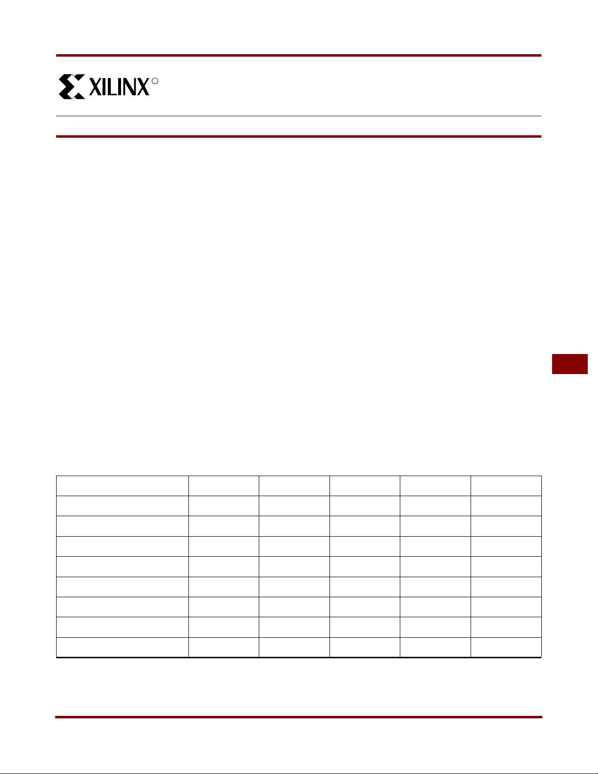
Table 1: XC5200 Field-Programmable Gate Array Family Members
the XC5200 Series and with the XC4000 Series
advanced BGA, TQ, and VQ packaging avail able
™
logic module,
7
Device XC5202 XC5204 XC5206 XC5210 XC5215
Logic Cells 256 480 784 1,296 1,936
Max Logic Gates 3,000 6,000 10,000 16,000 23,000
Typical Gate Range 2,000 - 3,000 4,000 - 6,000 6,000 - 10,000 10,000 - 16,000 15,000 - 23,000
VersaBlock Array 8 x 8 10 x 12 14 x 14 18 x 18 22 x 22
CLBs 64 120 196 324 484
Flip-Flops 256 480 784 1,296 1,936
I/Os 84 124 148 196 244
TBUFs per Longline 1014162024
November 5, 1998 (Version 5.2) 7-83
Page 2
XC5200 Series Field Programmable Gate Arrays
R
XC5200 Family Compared to
XC4000/Spartan™ and XC3000
Series
For readers alrea dy familiar with the XC4000/Spa rtan and
XC3000 FPGA Families, this section describes sig nificant
differences between them and the XC5200 family. Unless
otherwise indicated, comparisons refer to both
XC4000/Spartan and XC3000 devi ces.
Configurable Logic Block (CL B ) Resources
Each XC5200 CLB cont ai n s four i nde pe nde nt 4- inp ut fu nction generators and four registers, which are configured as
four indepe ndent L ogic Ce lls™ ( LCs). T he regi sters in eac h
XC5200 LC are optionally configurable as edge-triggered
D-type flip-flops or as transparent level-sensitive latches.
The XC5200 CLB includes dedicated carry logic that provides fast arithmetic ca rry capability. The dedicated carry
logic may also be used to cascade function generators for
implementing wide arithmetic functions.
XC4000 family:
decoders. Wide decoders are implemented using cascade
logic. Although sa crificing s peed for s ome desig ns, lack of
wide edge decoders reduces the die area and hence cost
of the XC5200.
XC4000/Spartan family:
differs from that o f the XC4000/Spar tan family in that the
sum is generated in an additional function generator in the
adjacent column. This design reduces XC5200 die size and
hence cost for many applications. Note, however, that a
loadable up/down counter requires the same number of
function gener ators in bo th families . XC3000 has no d edicated carry.
XC4000/Spartan family:
mized for cost and hence cannot implement RAM.
Input/Output Block (IOB) Resources
The XC5200 family maintains footprint compatibility with
the XC4000 family , but not with the XC3000 family.
T o minimize cost and maximize the number of I/O per Logic
Cell, the XC5200 I/O does not include flip-flops o r latches.
For high performance paths, the XC5200 family provides
direct connections from each IOB to the registers in the
adjacent CLB in order to emulate IOB registers.
Each XC5200 I/O Pin provides a programmable delay element to contro l input s et-up tim e. This element ca n be used
to avoid potential hold-time problems. Each XC5200 I/O
Pin is capable of 8-mA source and sink currents.
IEEE 1149.1-type boundary scan is supported in each
XC5200 I/O.
XC5200 devices have no wide edge
XC5200 dedicated carry logic
XC5200 lookup tables are opti-
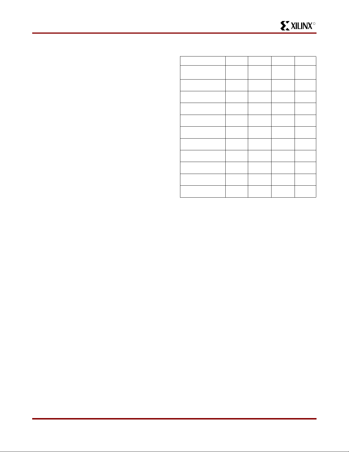
Table 2: Xilinx Field-Programmable Gate Array
Families
Parameter XC5200 Spartan XC4000 XC3000
CLB function
generators
CLB inputs 20 9 9 5
CLB outputs 12 4 4 2
Global buffers 4 8 8 2
User RAM no yes yes no
Edge decoders no no yes no
Cascade chain yes no no no
Fast carry logic yes yes yes no
Internal 3-state yes yes yes yes
Boundary scan yes yes yes no
Slew-rate control yes yes yes yes
4332
Routing Resources
The XC5200 family provides a flexible coupling of logic and
local routing res ourc es cal led the VersaB lock . The XC520 0
Ver saBlock elemen t incl udes t he CLB, a Loc al Inte rconne ct
Matrix (LIM), and direct connects to neighboring VersaBlocks.
The XC5200 provides four global buffers for clocking or
high-fanout co ntro l s igna l s. E a ch buffer may be sou rc ed by
means of its dedicated pad or from any internal source.
Each XC5200 TBUF ca n dr i ve up t o t wo h ori zo nt al a nd t wo
vertical Longlines. There are no internal pull-ups for
XC5200 Longlines.
Configuration and Readback
The XC5200 supports a new configuration mode called
Express mode.
XC4000/Spartan family:
global reset but not a global set.
XC5200 devices use a different configuration process than
that of the XC 30 00 f ami ly, but use t he same p ro ce ss as t he
XC4000 and Spartan families.
XC3000 family:
fer, XC5200 devices may be used in daisy chains with
XC3000 devices.
XC3000 family:
gle-function input pin that overrides all other inputs. The
PROGRAM pin does not exist in XC3000.
Although their configuration processes dif-
The XC5200 PROGRAM pin is a sin-
The XC5200 family provides a
7-84 November 5, 1998 (Version 5.2)
Page 3
R
XC5200 Series Field Programmable Gate Arrays
XC3000 family:
XC5200 devices support an additional pro-
gramming mode: Peripheral Synchronous.
XC3000 family:
The XC5200 family does not support
Power-down, but off ers a Gl obal 3- sta te input that does not
reset any flip-flops.
XC3000 family:
The XC5200 family does not provide an
on-chip crystal oscillato r amplifier, but it does provide an
internal oscillator fro m which a variet y of fre quencie s up to
12 MHz are available.
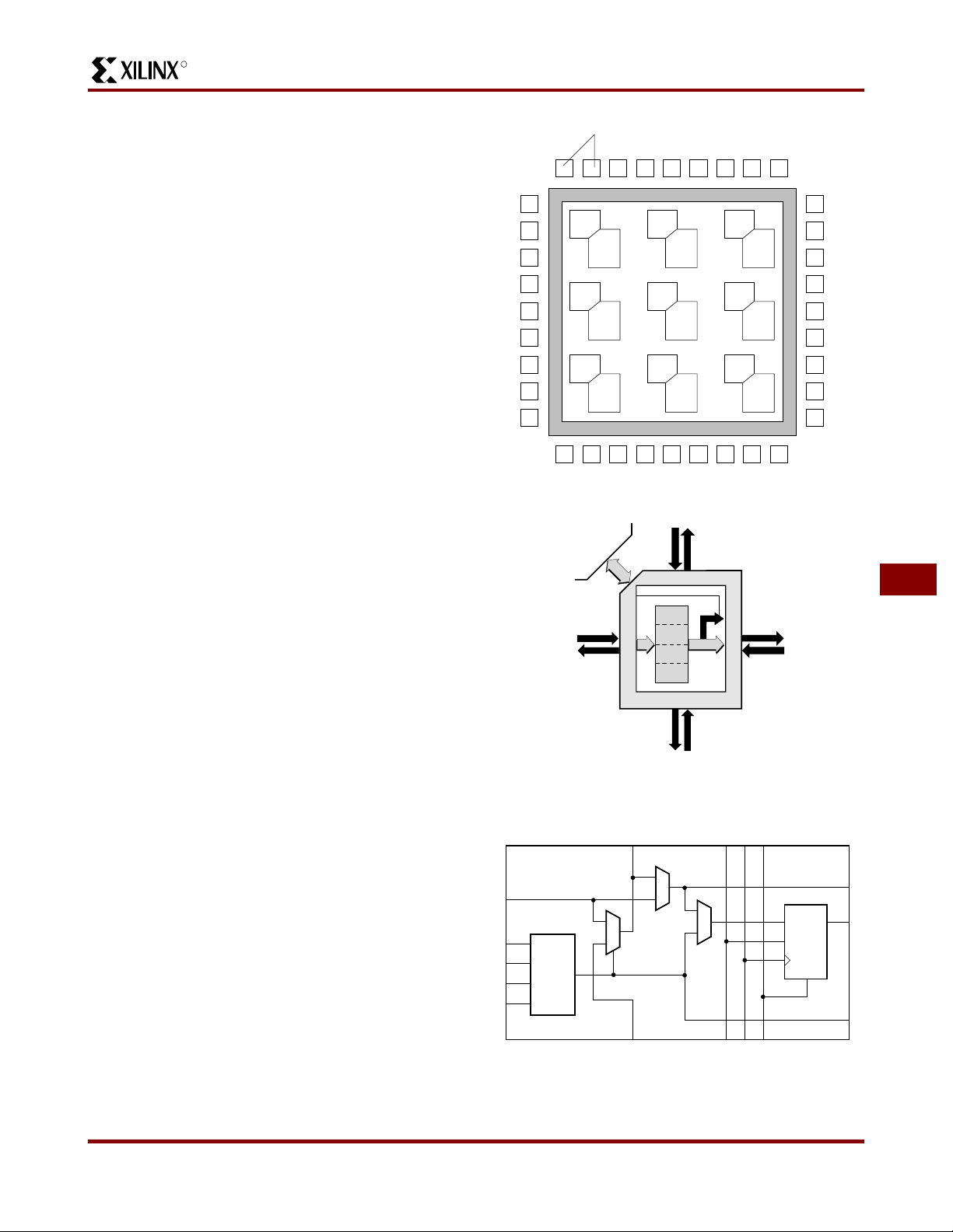
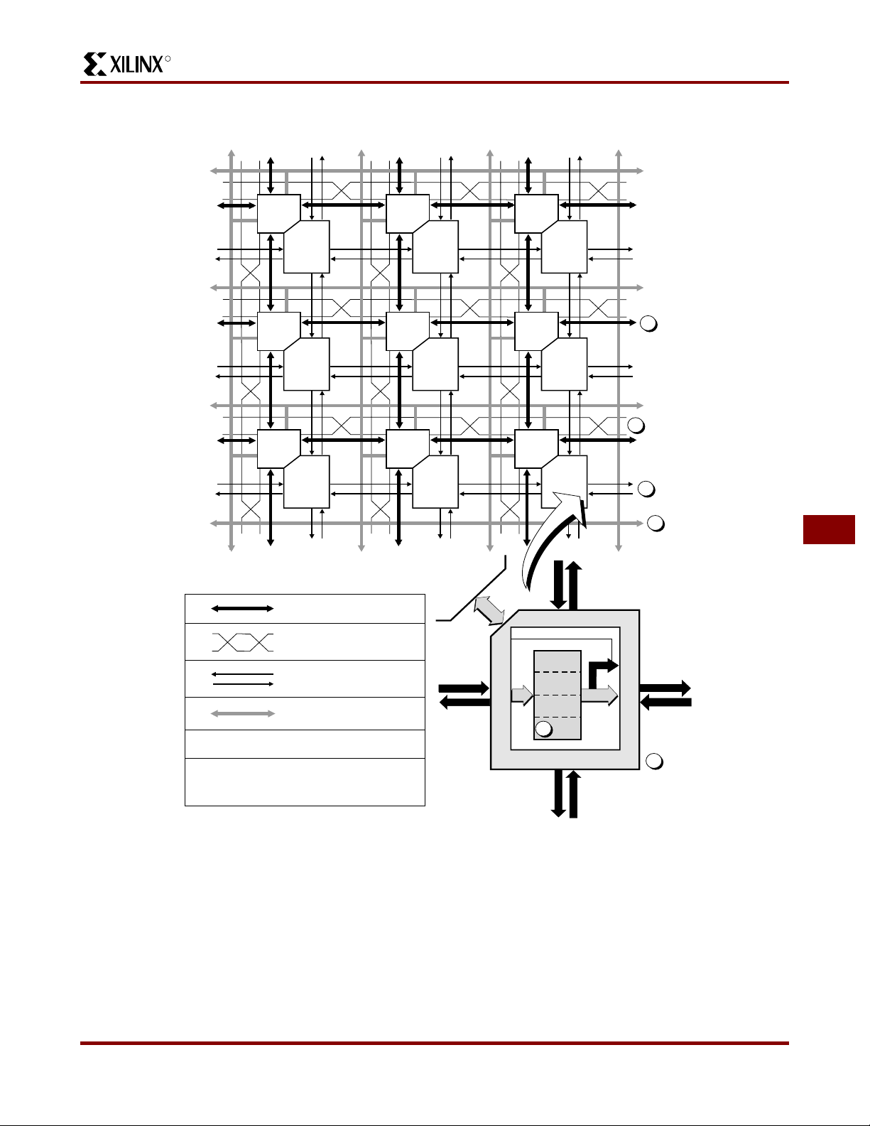
Architectural Overview
Figure 1 presents a simplified, conceptual overview of the
XC5200 architecture. Similar to conventional FPGAs, the
XC5200 family consists of programmable IOBs, programmable logic blocks, and programmable interconnect. Unlike
other FPGAs, however, the logic and local routing
resources of th e XC5200 family are combin ed in flexible
VersaBlocks (Figure 2). General-purpose routing connects
to the VersaBlock through the General Routing Matrix
(GRM).
VersaBlock: Abundant Local Routing Plus
V ersatile Logic
The basic logic elemen t in ea ch VersaBlock structure is the
Logic Cell, shown in Figure 3. Each LC contains a 4-input
function generator (F), a storage device (FD), and control
logic. There are five independent inputs and three outputs
to each LC. The independence of the inputs and outputs
allows the software to maximize the resource utilization
within each LC. Each Logic Cell also contains a direct
feedthrough path that does not sacrifice the use of either
the function gen erator or the register ; this featu re is a fi rst
for FPGAs. The st orage devic e is configu rable as eit her a D
flip-flop or a latch. The control logic consists of carry logic
for fast implementation of arithmetic functions, which can
also be configured as a cascade chain allowing decode of
very wide input functions.
Input/Output Blocks (IOBs)
VersaRing
GRM
GRM
VersaRing
GRM
Versa-
Block
Versa-
Block
Versa-
Block
GRM
Versa-
Block
GRM
Versa-
Block
GRM
Versa-
Block
VersaRing
GRM
GRM
GRM
Versa-
Block
Versa-
Block
Versa-
Block
Figure 1: XC5200 Architectural Overview
GRM
24
24
4
4
44
TS
CLB
LC3
LC2
LC1
LC0
44
Direct Connects
4
4
4
LIM
Figure 2: VersaBlock
VersaRing
X4955
7
X5707
CO
DI
DQ
F4
F3
F
F2
F1
CI CE CK CLR
DO
FD
X
X4956
Figure 3: XC5200 Logic Cell (Four LCs per CLB)
November 5, 1998 (Version 5.2) 7-85
Page 4
XC5200 Series Field Programmable Gate Arrays
R
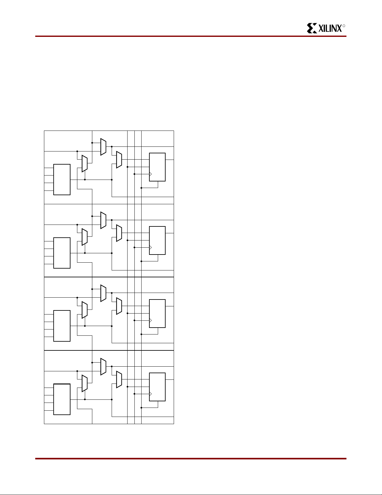
The XC5200 CLB consists of four LCs, as shown in
Figure 4. Each CLB has 20 independent inputs and 12
independent outputs. The top and bottom pairs of LCs can
be configured to implement 5-input functions. The challenge of FPGA implementation software has always been
to maximize the usage of logic resources. The XC5200
family addresses this issue by surrounding each CLB with
two types of local inter connect — the Local Interconne ct
Matrix (LIM) and direct connects. These two interconnect
resources, combine d with the CLB, form the VersaBlock,
represented in Fi gure 2.
CO
DO
DQ
FD
X
DI
F4
F3
F2
F1
LC3
F
LC2
DI
DQ
F4
F3
F
F2
F1
DO
FD
X
LC1
DI
F4
F3
F2
F1
DI
F4
F3
F2
F1
LC0
LC0
DQ
F
DQ
F
CI CE CK CLR
DO
FD
X
DO
FD
X
X4957
Figure 4: Configurable Logi c Block
The LIM provides 100% connectivity of the inputs and outputs of each LC in a given CLB. The benefit of the LIM is
that no general routing resources are required to connect
feedback paths within a CLB. The LIM connects to the
GRM via 24 bidirectional nodes.
The direct connects allow immediate connections to neighboring CLBs, once again without using any of the general
interconnect. These two layers of local routing resource
improve the granularity of the architecture, effectively making the XC5200 family a “sea of logic cells.” Each
Versa-Block has four 3-state buffers that share a common
enable line and directly drive horizontal and vertical Longlines, creating robust on-chip bussing capability. The
VersaBlock allows fast, local impleme ntation of log ic functions, effectively imple menting us er designs in a hier archical fashion. These resources also minimize local routing
congestion and improve the efficiency of the general interconnect, which is used for connecting larger groups of
logic. It is this combination of both fine-grain and
coarse-grain architecture attributes that maximize logic uti lization in the XC5200 family. This symmetrical structure
takes full advantage of the third metal layer, freeing the
placement software to pack user logic optimally with minimal routing rest rictions.
VersaRing I/O Interface
The interface between the IOBs an d core logic has been
redesigned in the XC5200 family. The IOBs are completely
decoupled from the core logic. The XC5200 IOBs contain
dedicated boundary-scan logic for added board-level testability, but do not include input or output registers. This
approach allows a maximum number of IOBs to be placed
around the device, improving the I/O-to-gate ratio and
decreasing the cost per I/O. A “freeway” of interconnect
cells surrounding the device forms the VersaRing, which
provides connec tions from the IOBs to the internal lo gic.
These incremental routing resources provide abundant
connections from each IOB to the nearest VersaBlock, in
addition to Longline connections surrounding the device.
The VersaRing eliminates the historic trade-off between
high logic utilization and pin placement flexibility. These
incremental edge re so urce s giv e u se rs incre ase d fle xibilit y
in preassigning (i.e., locking) I/O pins before completing
their logic designs. Th is ability acce lerates tim e-to-mar ket,
since PCBs and other system components can be manufactured concurrent with the logic design.
General Routing Matrix
The GRM is functionally similar to the switch matrices
found in other architectures, but it is novel in its tight coupling to the logic resources contained in the VersaBlocks.
Advanced simulation tools were used during the development of the XC5200 architecture to determine the optimal
level of routing resources required. The XC5200 family
contains six levels of interconnect hierarchy — a series of
7-86 November 5, 1998 (Version 5.2)
Page 5
R
XC5200 Series Field Programmable Gate Arrays
single-length lines, double-length lines, and Longlines all
routed through the GRM. The direct connects, LIM, and
logic-cell feedthrough are contained within each
Versa-Block. Throughout the XC5200 interconnect, an efficient multiplexing sc heme, in c ombination with thre e layer
metal (TLM), w as used to imp rove the overall efficiency of
silicon usage.
Performance Overview
The XC5200 family has been benchmarked with many
designs running synchronous clock rates beyond 66 MHz.
The performance of an y design depe nds on the circui t to be
implemented, a nd t he d ela y th ro ug h th e co m binat or ial and
sequential logic elements, plus the delay in the interconnect routing. A rough estimate of timing can be made by
assuming 3-6 ns per logic level, which includes direct-connect routing delays, depending on speed grade. More
accurate estimations can be made using the information in
the Switching Characteristic Guideline section.
Tak ing Ad van tage of Reconfiguration
FPGA devices can be recon figured to ch ange logi c fu nction
while resident in the s ystem. T his capab ility gives the system designer a new degree of freedom not available with
any other type of logic.
Hardware can be changed as easily as software. Design
updates or modifications are easy, and can be made to
products alrea dy in the fie ld. A n FPG A ca n ev en be re co nfigured dynamically to perform different functions at different times.
Reconfigurable logic can be used to implement system
self-diagnostics, creat e systems capable of being reconfigured for different environments or operations, or implement
multi-purpose hardware for a given application. As an
added benefit, using reconfigurable FPGA devices simplifies hardware design and debugging and shortens product
time-to-market.
Detailed Functional Description
Configurable Logic Blocks (CLBs)
Figure 4 shows the logic in the XC5200 CLB, which con-
sists of four Logic Cells (LC[3:0]). Each Logic Cell consists
of an independent 4-input Lookup Table (LUT), and a
D-Type flip-flop or latch with c ommon cloc k, clock enable ,
and clear, but individually selectable clock polarity. Additional logic features provided in the CLB are:
• An independent 5-input LUT by combining two 4-input
LUTs.
• High-speed carry propagate logic.
• High-speed pattern decoding.
• High-speed direct connection to flip-flop D-inputs.
• Individual selection of either a transparent,
level-sensitive latch or a D flip-flop.
• Four 3-state buffers with a shared Output Enable.
5-Input Functions
Figure 5 illustrates how the outputs from the LUTs from
LC0 and LC1 can be combined with a 2:1 multiplexer
(F5_MUX) to provide a 5-input function. The outputs from
the LUTs of LC2 and LC3 can be similarly combined.
CO
DI
I1
I2
I3
I4
I5
F4
F3
F2
F
F1
F5_MUX
DI
F4
F3
F
F2
F1
CI
5-Input Function
CKCE
D
D
CLR
DO
Q
FD
X
LC1
DO
FD
LC0
out
Q
Qout
X
X5710
7
Figure 5: Two LUTs in Parallel Combined to Create a
5-input Function
November 5, 1998 (Version 5.2) 7-87
Page 6
XC5200 Series Field Programmable Gate Arrays
carry out
A3
or
B3
A3 and B3
to any two
A2
or
B2
A2 and B2
to any two
A1
or
B1
A1 and B1
to any two
A0
or
B0
A0 and B0
to any two
0
CI
CO
D
CY_MUX
DQ
CY_MUX
D
CY_MUX
D
CY_MUX
CKCE CLR
carry in
DI
F4
F3
XOR
F2
F1
DI
F4
F3
XOR
F2
F1
DI
F4
F3
XOR
F2
F1
DI
F4
F3
XOR
F2
F1
FD
FD
FD
FD
DO
LC3
DO
LC2
DO
LC1
DO
LC0
carry3
Q
half sum3
X
carry2
half sum2
X
carry1
Q
half sum1
X
carry0
Q
half sum0
X
R
DI
F4
F3
XOR
F2
F1
CO
DO
Q
D
FD
sum3
X
LC3
DI
F4
F3
XOR
F2
F1
DO
DQ
FD
sum2
X
LC2
DI
F4
F3
XOR
F2
F1
DO
D
Q
FD
sum1
X
LC1
DI
F4
F3
F2
XOR
F1
CK
CI
CE CLR
DO
Q
D
FD
sum0
X
LC0
F=0
CY_MUX
Initialization of
carry chain (One Logic Cell)
X5709
Figure 6: XC5200 CY_MUX Used for Adder Carry Propagate
Carry Function
The XC5200 family supports a carry-logic feature that
enhances the performance of arithmetic functions such as
counters, adders, etc. A c arry m ultiple xer (CY_ MUX) symbol is used to indicate the XC5200 carry logic. This symbol
represents the dedicated 2:1 multiplexer in each LC that
performs the one-bit high-speed carry propagate per logic
cell (four bits per CLB).
While the carry propagate is performed inside the LC, an
adjacent LC must be used to complete the arithmetic function. Figure 6 represents an example of an adder function.
The carry propagate is performed on the CLB shown,
which also gener ates the hal f-su m for the four -bit ad der . An
adjacent CLB is responsible fo r XORing the half-su m with
the corresponding carry-out. Thus an adder or counter
requires two LCs per bit. Notice that the carry chain
requires an initialization stage, which the XC5200 family
accomplishes using the carry initialize (CY_INIT) macro
and one additional LC. The carry chain can propagate vertically up a column of CLBs.
The XC5200 library contains a set of Relationally-Placed
Macros (RPMs) and arithmetic func tions designed to take
advantage of the dedicated carry logic. Using and modifying these macros m akes it much easie r to implement cus-
7-88 November 5, 1998 (Version 5.2)
Page 7
R
XC5200 Series Field Programmable Gate Arrays
tomized RPMs, freeing the designer from the need to
become an expert on architectures.
cascade out
A15
A14
A13
A12
A11
A10
A9
A8
CO
DI
F4
F3
AND
F2
F1
DI
F4
F3
AND
F2
F1
DI
A7
F4
A6
F3
A5
A4
A3
A2
A1
A0
AND
F2
F1
DI
F4
F3
AND
F2
F1
F=0
CY_MUX
CY_MUX
CY_MUX
CY_MUX
CI
cascade in
CY_MUX
Initialization of
carry chain (One Logic Cell)
CK
CE CLR
DO
Q
D
FD
X
LC3
DO
DQ
FD
X
LC2
DO
D
Q
FD
X
LC1
DO
Q
D
FD
X
LC0
out
X5708
Figure 7: XC 5200 CY_MU X Used f or Decoder Cascade
Logic
Cascade Function
Each CY_MUX can be connected to the CY_MUX in the
adjacent LC to provide cascadable decode logic. Figure 7
illustrates how the 4- input func tion gene rator s can be configured to take advantage of these four cascaded
CY_MUXes. Note th at AND an d OR casca ding ar e speci fic
cases of a general decode. In AND cascading all bits are
decoded equal to logic one, while in OR cascading all bits
are decoded equ al to logic ze ro. The flexibility of the LUT
achieves this result. The XC5200 library contains gate
macros desig ned to take advantag e of this function.
CLB Flip-Flops and Latches
The CLB can pass the combinatorial output(s) to the interconnect network, but can also store the combinatorial
results or other incoming data in flip-flops, and connect
their outputs to the interconnect network as well. The CLB
storage elements can also be configured as latches.
Table 3: CLB Storage Element Functionality
(active rising edge is shown)
Mode CK CE CLR D Q
Power-Up or
GR
XXXX0
XX1X0
Flip-Flop
__/
1* 0* D D
0X0*XQ
Latch
11*0*XQ
01*0*DD
Both X 0 0* X Q
Legend:
X
__/
0*
1*
Don’t care
Rising edge
Input is Low or unconnected (default value)
Input is High or unconnecte d (default value)
Data Inputs and Outputs
The source of a storage element data input is programmable. It is driven by the function F, or by the Direct In (DI)
block input. The flip-flops or latches drive the Q CLB outputs.
Four fast feed-through paths from DI to DO are available,
as shown in Figure 4. This bypass is sometimes used by
the automated router to repower internal signals. In addition to the storage element (Q) and direct (DO) outputs,
there is a combinatorial output (X) that is always sourced
by the Lookup Table.
The four edge-triggered D-type flip-flops or level-sensitive
latches have common clock (CK) and clock enable (CE)
inputs. Any of the clock inputs can also be permanently
enabled. Storage element functionality is described in
Table 3.
Clock Input
The flip-flops ca n b e trig g ered o n e ith er th e risin g or fa lling
clock edge. The clock pin is shared by all four storage elements with individual polarity control. Any inverter placed
on the clock input is automatically absorbed into the CLB.
Clock Enable
The clock enable signal (CE) is active High. The CE pin is
shared by the four storage elements. If left unconnected
for any, the clock enable for that storage element defaults
to the active state. CE is not invertible within t he CLB.
Clear
An asynchrono us st orage ele ment i nput ( CLR) ca n be us ed
to reset all four flip- flops or latches in t he CLB. This input
7
November 5, 1998 (Version 5.2) 7-89
Page 8
XC5200 Series Field Programmable Gate Arrays
Figure 8: Schematic Symbols for Gl obal Reset
R
can also be indep en den tly dis ab l ed for any fl ip -f lop . C LR i s
active High. It is not invertible within the CLB.
STARTUP
PAD
IBUF
GR
GTS
CLK
Q2
Q3
Q1Q4
DONEIN
X9009
Global Reset
A separate Global Reset line clears each storage element
during power-up, reconfiguration, or when a dedicated
Reset net is driven active. This global net (GR) does not
compete with other routing resources; it uses a dedicated
distribution networ k.
GR can be driven from any user-programmable pin as a
global reset input. To use this global net, place an input pad
and input buffer in the schematic or HDL code, driving the
GR pin of the ST ARTUP symbol. (See Figure 9.) A specific
pin location can be assigned to this input using a LOC
attribute or property, just as with any other user-programmable pad. An inverter can optionally be inserted after the
input buffer to invert the sense of the Global Reset signal.
Alternatively, GR can be driven from any internal node.
Using FPGA Flip-Flops and Latches
The abundance of flip-flops in the XC5200 Series invites
pipelined desi gns. This is a po werful way of i ncreas in g performance by breaking the function into smaller subfunctions and e xecuting them in parallel, pa ssing on the re sults
through pipe li ne f li p- f lops . This me th od sh ould be se rio us l y
considered wherever throughput is more important than
latency.
To include a CLB flip-flop, place the appropriate library
symbol. For example, FD CE is a D-t y pe f li p-fl o p wit h cl ock
enable and asynchronous clear. The corresponding latch
symbol is called LDCE.
In XC5200-Series devices, the flip-flops can be used as
registers or shift registers without blocking the function
generators from performing a different, perhaps unrelated
task. This ability increases the functional capacity of the
devices.
The CLB setup time is specified between the function generator input s and the clock input CK. Therefore, the specified CLB flip-flop setup time includes the delay through the
function generator .
Three-State Buffers
The XC5200 family has four dedicated Three-State Buffers
(TBUFs, or BUFTs in the sche matic library) per CLB (see
Figure 9). The four buffers are individually configurable
through four configuration bits to operate as simple
non-inverting buffers or in 3-state mode. When in 3-state
mode the CLB output enable (TS) control signal drives the
enable to all four buffers. Each TBUF can drive up to two
horizontal an d/or t wo vertic al Lon glines . These 3- state buf fers can be used to implement multiplexed or bidirectional
buses on the horizontal or vertical longlines, saving logic
resources.
The 3-state buffer e nable is an active -High 3-sta te (i.e. an
active-Low enable), as shown in Table 4.
Table 4: Three-State Buffer Functionality
IN T OUT
X1Z
IN 0 IN
Another 3-stat e buffer with similar ac cess is located near
each I/O block al ong the right and left edges of the arra y.
The longlines driven by the 3-state buffers have a weak
keeper at each end. This circuit prevents undefined floating levels. However, it is overridden by any driver. To
ensure the lon glin e go es high when no bu ffers ar e on , a dd
an additional BUFT to drive the output Hi gh duri ng al l of t he
previously undefined states.
Figure 10 shows how to use the 3-state buffers to imple-
ment a multiplexer. The selection is acco mplished by the
buffer 3-state signal.
TS
CLB
CLB
LC3
LC2
LC1
LC0
Horizontal
Longlines
X9030
7-90 November 5, 1998 (Version 5.2)
Figure 9: XC5200 3-State Buffers
Page 9
R
I
O
T
PAD
Vcc
X9001
Input
Buffer
Delay
Pullup
Pulldown
Slew Rate
Control
Output
Buffer
XC5200 Series Field Programmable Gate Arrays
• A + DB • B + DC • C + DN • N
Z = D
~100 k
Ω
A
D
N
"Weak Keeper"
D
A
ABCN
BUFT BUFT BUFT BUFT
D
B
D
C
Figure 10: 3-State Buffers Implement a Multip lexer
Input/Output Blocks
User-configurable input/output blocks (IOBs) provide the
interface betwee n external package pins and the intern al
logic. Each IOB controls one package pin and can be configured for input, output, or bidirectional si gnals.
The I/O block, shown in Figure 11, consists of an input
buffer and an output buffer. The output driver is an 8-mA
full-rail CMOS buffer with 3-state control. Two slew-rate
control modes are supported to minimize bus transients.
Both the o utput bu ffer and the 3-state cont ro l a re in ve rt ibl e .
The input buffer has globally selected CMOS or TTL input
thresholds. T he input bu ffer is invertib le and also provides a
programmable delay line to assure reliable chip-to-chip
set-up and hold times. Minimum ESD protec tion is 3 KV
using the Human Body Model.
Figure 11: XC5200 I/O Block
IOB Input Signals
The XC5200 inputs can be globally configured for either
TTL (1.2V) or CMOS thresholds, using an option in the bitstream generation software. There is a slight hysteresis of
about 300mV.
The inputs of XC5200-Series 5-Volt devices can be driven
by the outputs o f any 3. 3-V olt device, if the 5- V olt inputs ar e
in TTL mode.
Supported sources for XC5200-Series device inputs are
shown in Table 5.
November 5, 1998 (Version 5.2) 7-91
Table 5: Supported Sources for XC520 0-Series Device
Inputs
XC5200 Input Mode
Source
Any device , Vcc = 3.3 V,
CMOS outputs
Any device, Vcc = 5 V,
TTL outputs
Any device, Vcc = 5 V,
CMOS outputs
5 V,
TTL
√
√
√√
Optional Delay Guarantees Zero Hold Time
XC5200 devices do no t have st orage el ements in the IOB s.
However, XC5200 IOBs can be efficiently routed to CLB
flip-flops or latches to store the I/O signals.
The data input to the re gister can o ption ally be delaye d by
several nanoseconds. With the delay enabled, the setup
time of the input flip-flop is increa sed so tha t normal clock
routing does not result in a positive hold-time requirement.
A positive hold time requirement can lead to unreliable,
temperature- or processing-dependent operation.
The input flip-flop setup time is defined between the data
measured at the de vice I/O pin and the clock inpu t at the
CLB (not at the clock pin). Any routing delay from the
device clock pin to the clock input of the CLB must, therefore, be subtracted from this setup time to arrive at the real
setup time requirement relative to the device pins. A short
specified setup time might, therefore, result in a negative
setup time at the device pins, i.e., a positive hold-time
requirement.
When a delay is i nser t ed on th e data l ine , mor e c loc k de lay
can be tolerated without causing a positive hold-time
requirement. Sufficient de lay eliminat es the poss ibility of a
data hold-time requirement at the external pin. The maximum delay is therefore inserted as the software default.
The XC5200 IO B has a one-ta p delay elemen t: either the
delay is insert ed (defau lt), or i t is not. The dela y guarante es
a zero hold time with respect to clocks routed through any
of the XC5200 global clock buffers. (See “Global Lines” on
page 96 for a description of the global clock buffers in the
XC5200.) For a shorter input register setup time, with
X6466
5 V,
CMOS
Unreliable
Data
7
Page 10
XC5200 Series Field Programmable Gate Arrays
Figure 12: Open-Drain Output
R
non-zero hold, attach a NODELAY attribute or property to
the flip-flop or input buffer.
IOB Output Signals
Output signals can be optionally inverted within the IOB,
and pass directly to the pad. As with the inputs, a CLB
flip-flop or latch can be used to store the output signal.
An active-High 3-state signal can be used to place the output buffer in a high-impedance state, implementing 3-state
outputs or bidirectional I/O. Under configuration control,
the output (OUT) and output 3-state (T) signals can be
inverted. The polarity of these signals is independently
configured for each IOB.
The XC5200 devi ces p rovid e a gua rant eed out put sink c urrent of 8 mA.
Supported destinations for XC5200-Series device outputs
are shown in Table 6.(For a detailed disc ussion of how to
interface between 5 V and 3.3 V devices, see the 3V Products section of
The Programmable Logic Data Book
An output can be co nfi gure d as ope n-dr ain (open -coll ect or)
by placing an OBUFT symbol in a schematic or HDL code,
then tying the 3-state pin (T) to the output signal, and the
input pin (I) to Ground. (See Figure12.)
Table 6: Supported Destinations for XC5200-Series
Outputs
XC5200 Output Mode
Destination
XC5200 device, V
=3.3 V,
CC
CMOS
CMOS-threshold inputs
Any typical devi ce, V
CMOS-threshold inputs
= 3.3 V,
CC
some
Any device, VCC = 5 V,
TTL-threshold inputs
Any device, V
CC
= 5 V,
CMOS-threshold inputs
1. Only if destination device has 5-V tolerant input s
OPAD
OBUFT
X6702
.)
5 V,
√
1
√
√
For XC5200 devices, maximum total capacitive load for
simultaneous fast mode switching in the sam e direction is
200 pF for all packag e pins between eac h Power/Ground
pin pair. For some XC5200 devices, additional internal
Power/Ground pin pairs are connected to special Power
and Ground planes within the packages, to reduce ground
bounce.
For slew-rate limited outputs this total is two times larger for
each device type: 400 pF for XC5200 devices. This maximum capacitive load should not be exceeded, as it can
result in ground bounce of grea ter than 1. 5 V amplitud e and
more than 5 ns duration. This level of ground bounce may
cause undesired transient behavior on an output, or in the
internal logic. This r estriction is comm on to all high-spe ed
digital ICs, and is not particular to Xilinx or the XC5200
Series.
XC5200-Series devices have a feature called “Soft
Start-up,” de signed to r educe gr ound bo unce when al l ou tputs are turned on simultaneously at the end of configuration. When the configuration process is finished and the
device starts up, the first activation of the outputs is automatically slew-rate limited. Immediately following the initial
activation of the I/O, the slew rate of the individual outputs
is determined by the individual configuration option for
each IOB.
Global Three-State
A separate Global 3-State line (not shown in Figure 11)
forces all FPGA outputs to the high-impedance state,
unless boundary scan is enabled and is executing an
EXTEST instruction. This global net (GTS) does not compete with othe r rou tin g resou rces ; it u ses a dedic ate d di stribution network.
GTS can be driven from any user-programmable pin as a
global 3-state input. To use this global net, place an input
pad and input buffer in the schematic or HDL code, driving
the GTS pin of the STARTUP symbol. A specific pin location can be assigned to this input using a LOC attribute or
property, just as with any ot her us er-prog rammabl e pad. A n
inverter can optionally be inserted after the input buffer to
invert the sens e of the Gl obal 3- State si gnal. Us ing GTS is
similar to Global Reset. See Figure 8 on page 90 for
details. Alternatively, GTS can be driven from any internal
node.
Other IOB Options
There are a number of other programmable options in the
XC5200-Series IOB.
Output Slew Rate
The slew rate of each output buffer is, by default, reduced,
to minimize power bus tran sient s when switching no n-cr itical signals. For critical sig nals, attach a FAST attribute or
property to the output buffer or flip-flop.
7-92 November 5, 1998 (Version 5.2)
Pull-up and Pull-down Resistors
Programmable IOB pull-up and pull-down resistors are
useful for tying unused pins to Vcc or Ground to minimize
power consumption and reduce noise sensitivity. The configurable pull-up resistor is a p-channel transistor that pulls
Page 11
R
to Vcc. The confi gurabl e pull-d own resi stor is an n-chan nel
transistor that pulls to Ground.
The value of these resistors is 20 kΩ − 100 kΩ. This high
value makes them uns uitable as wired-AND pu ll-up resistors.
The pull-up resi stor s for most u ser-pr ogrammabl e IOBs ar e
active during th e configuration process. See Table 13 on
page 124 for a list of pins with pull-ups ac tive before and
during configuration.
After configuration, voltage levels of unused pads, bonded
or unbonded, must be valid logic levels, to reduce noise
sensitivity and avoid excess current. Therefore, by default,
unused pads are configured with the internal pull-up resistor active. Alternatively, they can be individually configured
with the pull-down resistor, or as a driven output, or to be
driven by an external source. To activate the internal
pull-up, attach the PULLUP library component to th e net
attached to the pad. To activate the internal pull-down,
attach the PULLDOWN library component to the net
attached to the pad.
JTAG Support
Embedded logic attached to the IOBs contains test structures compatible with IEEE Standard 1149.1 for boundary
scan testing, simplifying board-level testing. More information is provided in “Boundary Scan” on page 98.
Oscillator
XC5200 devices include a n internal os cillator. This oscillator is used to clock the powe r-on time-ou t, cl ear co nfigu ration memory, and source CCLK in Master configuration
modes. The oscillator ru ns at a nom in al 1 2 M Hz fr e quen cy
that varies with process, Vcc, and temperature. The output
CCLK frequency is selectable as 1 MHz (default), 6 MHz,
or 12 MHz.
The XC5200 oscillator divides the internal 12-MHz clock or
a user clock. The user then has the choice of dividing by 4,
16, 64, or 256 for the “OSC1” output and dividing by 2, 8,
32, 128, 1024, 4096, 16384, or 65536 for the “OSC2” output. The division is specified via a “DIVIDEn_BY=x”
attribute on the symbol, where n=1 for OSC1, or n=2 for
OSC2. These frequencies can vary by as much as -50% or
+ 50%.
The OSC5 macro is used where an internal oscillator is
required. The CK_DIV macro is applicable when a user
clock input is specified (see Figure 13).
XC5200 Series Field Programmable Gate Arrays
OSCS
CK_DIV
Figure 13: XC5200 Oscillator Macros
OSC1
OSC2
OSC1
OSC2
5200_14
VersaBlock Routing
The General Routing Matrix (GRM) connects to the
Versa-Block via 24 bidirectional ports (M0-M23). Excluding
direct connections, global nets, and 3-statable Longlines,
all VersaBlo ck i np ut s and ou tp ut s con nect to th e GR M vi a
these 24 ports. Four 3-statable unidirectional signals
(TQ0-TQ3) drive out of the VersaBlock directly onto the
horizontal and vertical Longlines. Two horizontal global
nets and two vertical global nets connect directly to every
CLB clock pin; the y can conn ect to other CLB inpu ts via th e
GRM. Each CLB also has four unidirectional direct connects to each of its four neighboring CLBs. These direct
connects can also feed directly back to the CLB (see
Figure 14).
In addition, ea ch C LB ha s 1 6 dir ec t in p ut s, four direct co n nections from each of the neighboring CLBs. These direct
connections provide high-speed local routing that
bypasses the GRM.
Local Interconnect Matrix
The Local Inter connec t Matrix (L IM) is b uilt from in put and
output multiplexers. The 13 CLB outputs (12 LC outputs
plus a V
outputs via the output multiplexers, which consist of eight
fully populated 13-to-1 multiplexers. Of the eight
VersaBlock outputs, four signals drive each neighboring
CLB directly, and provide a di rect feedba ck path to the input
multiplexers. The four remaining multiplexer outputs can
drive the GRM through four TBUFs (TQ0-TQ3). All eight
multiplexer outputs can connect to the GRM through the
bidirection al M0- M23 s ign al s. A ll eigh t s igna l s a l so c onne ct
to the input multiplexers and are potential inputs to that
CLB.
/GND signal) connect to the eight VersaBlock
cc
7
November 5, 1998 (Version 5.2) 7-93
Page 12
XC5200 Series Field Programmable Gate Arrays
To GRM
M0-M23
R
Direct West
Global Nets
North
South
East
West
Direct North
4
4
4
4
4
4
4
4
Feedback
4
24
Input
Multiplexers
8
TS
CLK
CE
CLR
4
C
OUT
CLB
5
5
5
5
LC3
LC2
LC1
LC0
C
IN
3
3
V
/GND
CC
3
3
Output
Multiplexers
8
To
Longlines
4
and GRM
TQ0-TQ3
Direct to
4
East
4
Direct South
Figure 14: VersaBlock Details
CLB inputs have several possible sources: the 24 signals
from the GRM, 16 direct connections from neighboring
VersaBlocks, four signals from global, low-skew buffers,
and the four signals from the CLB output multiplexers.
Unlike the output multiplexers, the input mu ltiplexers are
not fully populated; i.e., only a subset of the available signals can be con nected to a give n CL B input. The flexibility
of LUT input swapping and LUT mapping compensates for
this limitation. For example, if a 2-input NAND gate is
required, it can be mapped into any of the four LUTs, and
use any two of the four inputs to the LUT.
Direct Connects
The unidirectional direct-connect segments are connected
to the logic input/output pins through the CLB input and output multiple xe r ar ra ys, and th us bypa ss t he g ene ra l rou t ing
matrix altogether. These lines increase the routing channel
utilization, while simultaneously reducing the delay
incurred in speed-critical connections.
X5724
The direct connects also provide a high-speed path from
the edge CLBs to the VersaRing input/output buffers, and
thus reduce pin-to-pin set-up time, clock-to-out, and combinational prop agation delay. Direct connects from the input
buffers to the CLB DI pin (direct flip-flop input) are only
available on the left and right edges of the device. CLB
look-up table inputs and combinatorial/registered outputs
have direct connects to input/output buffers on all four
sides.
The direct connects are ideal for developing customized
RPM cells. Using direct connects improves the macro performance, and leaves the other routing channels intact for
improved routing. Direct connects can also route through a
CLB using one of th e four cell-fee dthrough paths.
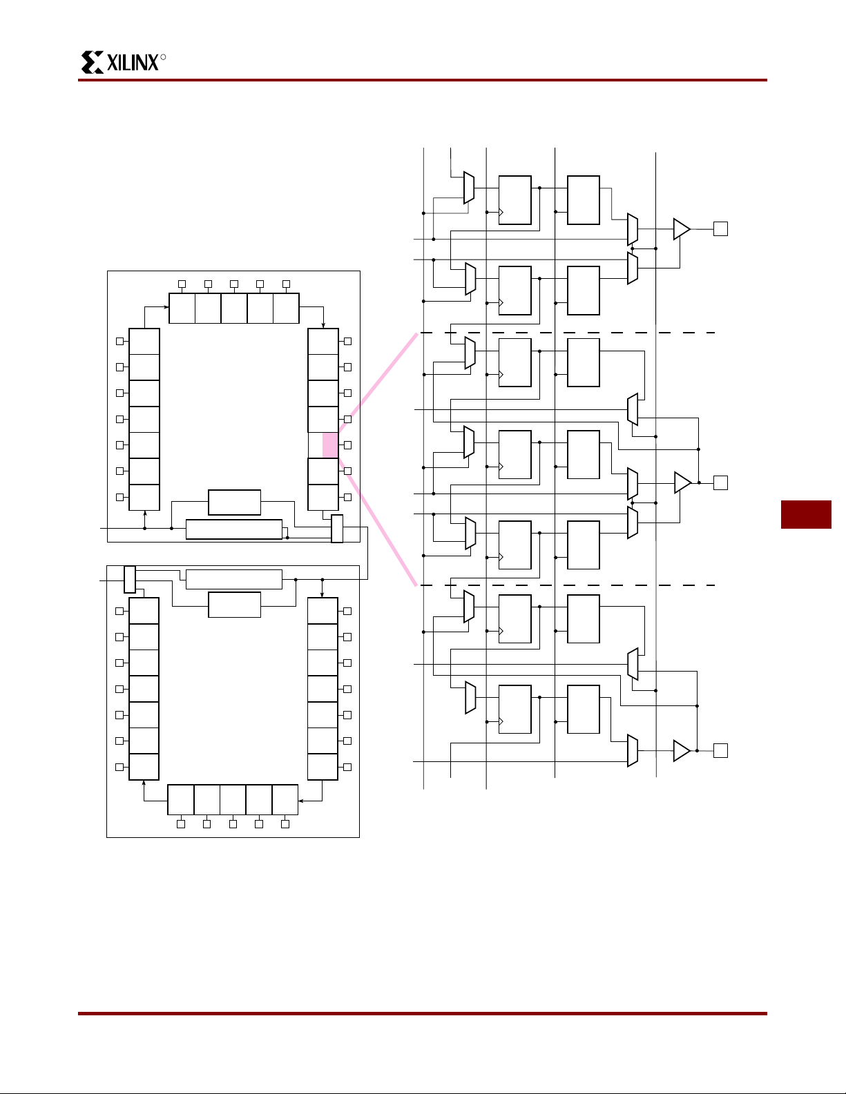
General Routing Matrix
The General R outing Matrix, shown in Figure 15, provide s
flexible bidirectio nal connect ions to th e Local Int erconnect
7-94 November 5, 1998 (Version 5.2)
Page 13
R
Matrix through a hierarchy of different-length metal segments in both the horizontal and vertical directions. A pro-
XC5200 Series Field Programmable Gate Arrays
GRM
Versa-
Block
GRM
Versa-
Block
GRM
Versa-
Block
Six Levels of Routing Hierarchy
1
2
3
4
LIM5
6
Single-length Lines
Double-length Lines
Direct Connects
Longlines and Global Lines
Local Interconnect Matrix
Logic Cell Feedthrough
Path (Contained within each
Logic Cell)
GRM
GRM
GRM
Versa-
Block
Versa-
Block
Versa-
Block
GRM
4
4
GRM
Versa-
Block
GRM
Versa-
Block
1
2
GRM
Versa-
Block
44
24
24
TS
CLB
LC3
4
LC2
LC1
6
LC0
44
LIM
3
4
4
4
7
5
Direct Connects
X4963
Figure 15: XC5200 Interconnect Structure
grammable interconnect point (PIP) establishes an electrical connection between two wire segments. The PIP, consisting of a pass transisto r switch controlled by a mem ory
element, provides bidirectional (in some cases, unidirectional) connection between two adjoining wires. A collection of PIPs inside the General Routing Matrix and in the
Local Interconnect Matrix provides connectivity between
various types of metal segments. A hierarchy of PIPs and
associated routing segments combine to provide a powerful interco nnect hierarchy:
• Forty bidi rectional single-length segments per CLB
provide ten routing channels to each of the four
neighboring CLBs in four directions.
• Sixteen bidirectional double-length segments per CLB
provide four r outing channels to each of four other
(non-neighbor ing ) CL B s in fou r direc tio ns.
• Eight horizontal and eight vertical bidirectional Longline
November 5, 1998 (Version 5.2) 7-95
Page 14
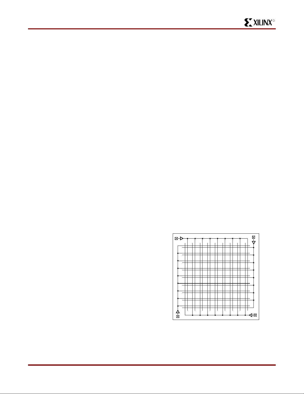
XC5200 Series Field Programmable Gate Arrays
R
segments span the width and height of the chip,
respectively.
Two low-skew horizontal and vertical unidirectional global-line segments span each row and co lumn of the chip,
respectively.
Single- and Double-Length Lines
The single- and double-length bidirectional line segments
make up the bulk of the routing channels. The double-length lines hop across every other CLB to reduce the
propagation del ays i n spe ed-cri tic al ne ts. R egenerat ing the
signal strength is recommended after traversing three or
four such segm ents. X ilinx place- and-route software a utomatically connects buffers in the path of the signal as necessary. Single- and double-len gth lines cannot drive onto
Longlines and global lines; Longlines and global lines can,
however, drive onto single- and double-length lines. As a
general rule, Longline and global-line connections to the
general routing matrix are unidirectional, with the signal
direction from these lines toward the routing matrix.
Longlines
Longlines ar e used for hig h-fan-o ut sig nals, 3 -state b usses,
low-skew nets, and faraway destinations. Ro w and column
splitter PIP s in the mid dle of the ar ray ef fecti vely doub le the
total number of Longlines by electrically dividing them into
two separated half-lines. Longlines are driven by the
3-state buffers in ea ch CLB, and are driv en by similar buffers at the periphery of the array from the VersaRing I/O
Interface.
Bus-oriented desi gns ar e easil y impl emented by using Longlines in conju ncti on wi th t he 3 -st ate buf fers in th e CLB and
in the VersaRing. Additionally, weak keeper cells at the
periphery reta in the last valid logic level on the Longlin es
when all buffers are in 3-state mode.
Longlines connect to the single-length or double-length
lines, or to the logic inside the CLB, through the General
Routing Matrix. The only manner in which a Longline can
be driven is through the four 3-state buffers; therefore, a
Longline-to-Longline or single-line-to-Longline connection
through PIPs in the General Routing Matrix is not possible.
Again, as a general rule, long- and global-line connections
to the General Routing Matrix are unidirectional, with the
signal direction from these lines toward the routing matrix.
carry/cascade logic described above, implementing a wide
logic function in p lace of the wired func tion. In the c ase of
3-state bus a pplicat ions, t he user must in sure th at all s tates
of the multiplexing function are defined. This process is as
simple as adding an additional TBUF to drive the bus High
when the previously undefined states are activated.
Global Lines
Global buffers in Xilinx FPGAs are special buffers that drive
a dedicated routing network called Global Lines, as shown
in Figure 16. This network is intended for high-fanout
clocks or other c ontrol signals , to maxim ize spe ed and minimize skewing while distributi ng the signal to many loads.
The XC5200 family has a total of four global buffers (BUFG
symbol in the library), each with its own dedicated routing
channel. Two are distributed vertically and two horizontally
throughout the FPGA.
The global lines provide direct input only to the CLB clock
pins. The global lines also connect to the General Routing
Matrix to provide ac cess from these lines to the function
generators and other control signa ls.
Four clock input pads at the corners of the chip, as shown
in Figure16, provide a high-spe ed, low -skew c lock net work
to each of the four global-line buffers. In addition to the dedicated pad, the global lines can be sourced by internal
logic. PIPs from several routing channels within the VersaRing can also be configured to drive the global-line buffers.
Details of all the programmable interconnect for a CLB is
shown in Figure 17.
GCK1
GCK4
The XC5200 famil y h as no p ull -u ps o n t he e nds o f t he Lon glines sourced by TBUFs, unlike the XC4000 Series. Consequently, wired functions (i. e. , WAND and WORAND) and
wide multiplexing functions requiring pull-ups for undefined
states (i.e ., b us ap pli c ati on s) must be imp l eme nt ed i n a dif ferent way. In the case of the wired functions, the same
functionality can be achieved by taking advantage of the
GCK2
Figure 16: Global Lines
GCK3
X5704
7-96 November 5, 1998 (Version 5.2)
Page 15
R
XC5200 Series Field Programmable Gate Arrays
.
x9010
SINGLE LONG
CARRY
DOUBLEGLOBAL
DIRECT
CLB
7
DIRECT
DIRECT
LONG
GLOBAL
DOUBLE
SINGLE
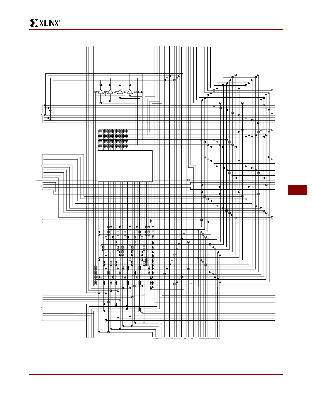
Figure 17: Detail of Programmable Interconnect Associated with XC5200 Series CL B
November 5, 1998 (Version 5.2) 7-97
Page 16
XC5200 Series Field Programmable Gate Arrays
R
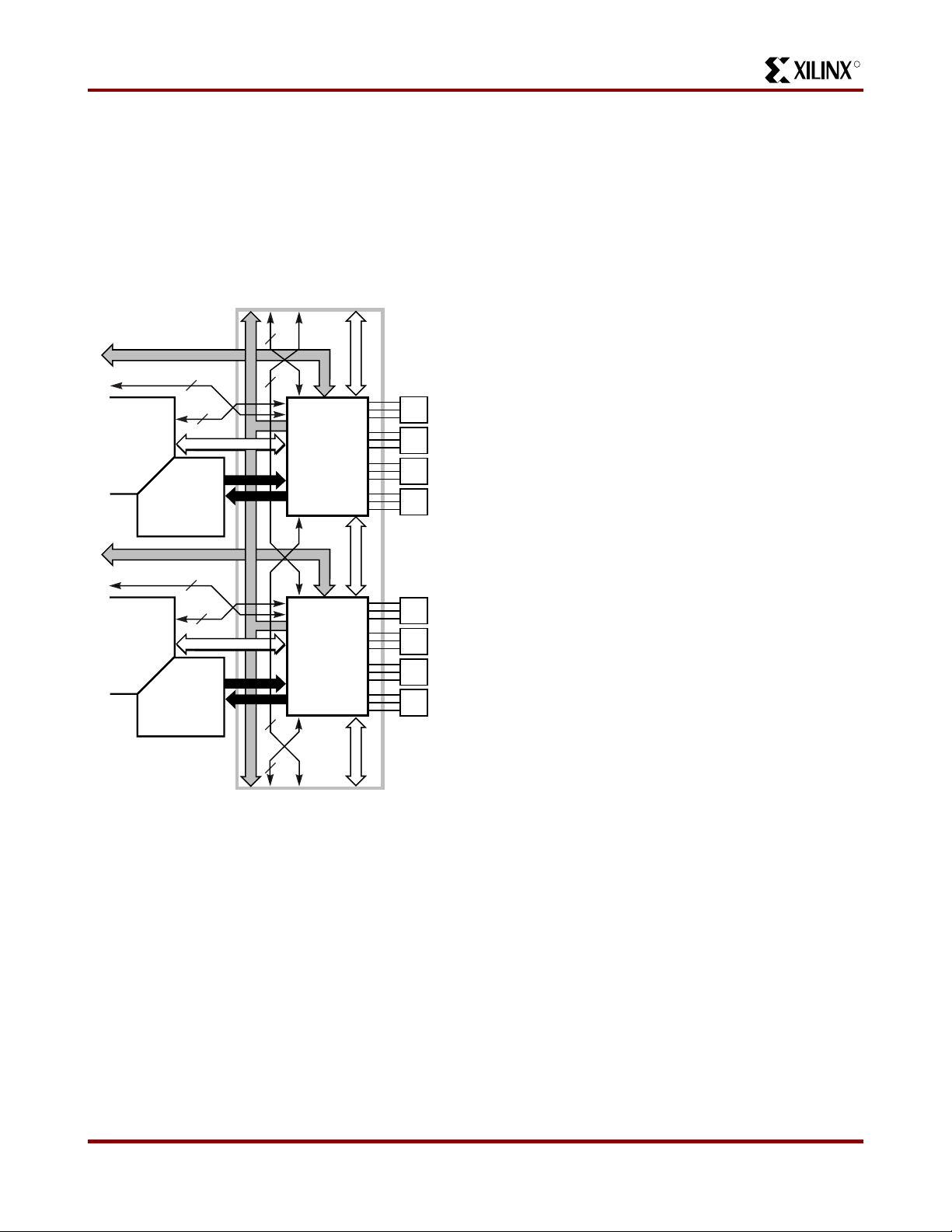
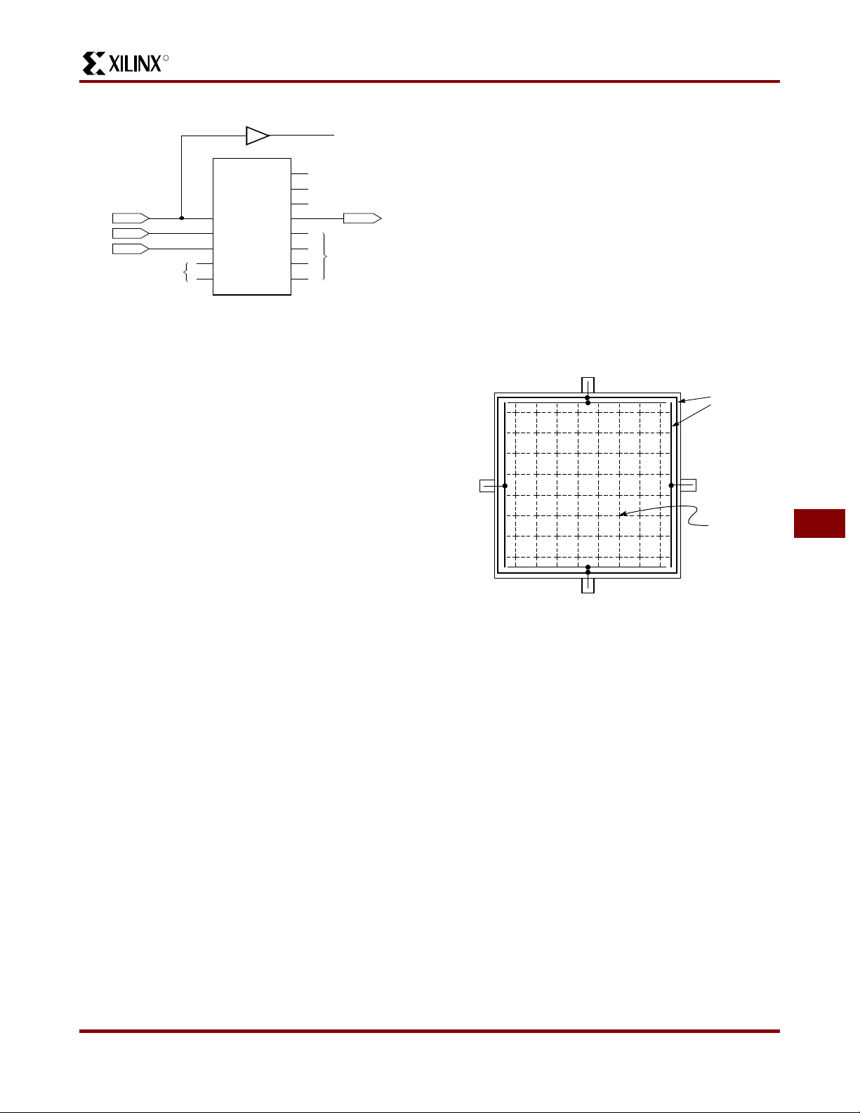
VersaRing Input/Output Interface
The VersaRing, shown in Figure 18, is positioned between
the core logic and the pad ring; it has all the routing
resources of a VersaBlock without the CLB logic. The VersaRing decouples the core logic from the I/O pads. Each
VersaRing Cell provides up to four pad-cell connections on
one side, and connects directly to the CLB ports on the
other side.
VersaRing
2
8
8
2
2
GRM
VersaBlock
2
2
GRM
VersaBlock
2
10
8
10
8
Interconnect
4
4
Interconnect
4
4
2
2
Figure 18: VersaRing I/O Interfac e
8
Pad
Pad
Pad
Pad
8
Pad
Pad
Pad
Pad
8
X5705
Boundary Scan
The “bed of nails” has been the trad itional method of test ing
electronic assemblies. This approach has become less
appropriate, due to closer pin spacing and more sophisticated assembly methods like surface-mount technology
and multi-layer boards. The IEEE boundary scan standard
1149.1 was developed to facilitate board-level testing of
electronic assemblies. Design and test engineers can
imbed a standard test logic structure in their device to
achieve high fault coverage for I/O and internal logic. This
structure is easily implemented with a four-pin interface on
any boundary sca n-compatib le IC. IEEE 1149.1-compatibl e
devices may be serial daisy- chaine d toget her , connec ted in
parallel, or a combination of the two.
XC5200 devices support all the mandatory boundary-scan
instructions specified in the IEEE standard 1149.1. A Test
Access Port (TAP) and registers are provided that implement the EXTEST, SAMPLE/PRELOAD, and BYPASS
instructions. The TAP can also s upport two USERCODE
instructions. When the boundary scan configuration option
is selected, three normal user I/O pins become dedicated
inputs for these functions. Another user output pin
becomes the dedicated boundary scan output.
Boundary-scan operation is independent of individual IOB
configuration and package type. All IOBs are treated as
independently controlled bidirectional pins, including any
unbonded IOBs. R etaining the bidirection al test capability
after configura tion provides flexibility for interconnect te sting.
Also, internal signals can be captured during EXTEST by
connecting them to unbonded IOBs, or to the unused outputs in IOBs used as unidirectional input pins. This technique partially compensates for the lack of INTEST
support.
The user can serially load commands and data into these
devices to control the driving of their outputs and to examine their inputs. This method is an improvement over
bed-of-nails testing. It avoids the need to over-drive device
outputs, and it reduces the user interface to four pins. An
optional fift h pin, a rese t for the c ontrol lo gic, is describe d in
the standard but is not implemented in Xilinx devices.
The dedicated on-chip logic implementing the IEEE 1149.1
functions in cl udes a 16- st a te machi n e, an ins tr uc t ion r eg i ster and a number of data registers. The functional details
can be found in the IEEE 1149.1 specification and are also
discussed in the Xilinx application note XAPP 017:
“Bound-
ary Scan in XC4000 and XC5200 Series devices”
Figure 19 on page 99 is a diagram of the XC5200-Series
boundary scan logic. It includes three bits of Data Register
per IOB, the IEEE 11 49.1 Tes t Access Port controller, and
the Instruction Register with decodes.
The public boundary-scan instructions are always available
prior to confi gurati on. Afte r config uration, the pub lic ins tructions and any USERCODE instructions are only available if
specified in the design. While SAMPLE and BYPASS are
available during configuration, it is recommended that
boundary-scan operations not be performed during this
transitory period.
In addition to the test instructions outlined above, the
boundary-sca n circui try can be used t o config ure the FPGA
device, and to read back the configuration data.
All of the XC4000 boundary-scan modes are supported in
the XC5200 family. Three additional outputs for the UserRegister are provided (Reset, Update, and Shift), repre-
7-98 November 5, 1998 (Version 5.2)
Page 17
R
senting the decoding of the corresponding state of the
boundary-scan internal state machine.
XC5200 Series Field Programmable Gate Arrays
DATA IN
IOB IOB
IOB
IOB
IOB
IOB
IOB
IOB
IOB
TDI
M
U
TDO
X
IOB
IOB
IOB
IOB
IOB
IOB
IOB IOB
IOB IOB IOB IOB IOB
IOB IOB IOB
BYPASS
REGISTER
INSTRUCTION REGISTER
INSTRUCTION REGISTER
BYPASS
REGISTER
IOB
IOB
IOB
IOB
IOB
IOB
IOB
IOB
IOB
IOB
IOB
IOB
IOB
1
D Q
0
IOB.O
IOB.T
IOB.I
IOB.O
M
TDO
U
X
TDI
IOB.T
IOB.I
IOB.O
SHIFT/
CAPTURE
1
D Q
0
1
D Q
0
1
D Q
0
1
D Q
0
1
D Q
0
1
D Q
0
DATAOUT UPDATE EXTEST
CLOCK DATA
REGISTER
sd
DQ
LE
sd
DQ
LE
sd
DQ
LE
sd
DQ
LE
sd
DQ
LE
sd
DQ
LE
sd
DQ
LE
1
0
0
1
1
0
1
0
0
1
1
0
0
1
7
X1523_01
Figure 19: XC5200-Series Boundary Scan Logic
November 5, 1998 (Version 5.2) 7-99
Page 18
XC5200 Series Field Programmable Gate Arrays
R
XC5200-Seri es devi ces c an a lso be conf igu red t hrou gh t he
boundary scan logic. See XAPP 017 for more information.
Data Registers
The primary data register is the boundary scan register.
For each IOB pin in the FPGA, bonded or not, it includes
three bits for In , Out and 3-State Contro l. Non-IOB pins
have appropriate partial bit population for In or Out only.
PROGRAM
boundary scan register. Each EXTEST CAPTURE-DR
state captur es all In, Out, and 3-State pins.
The data register also includes the following non-pin bits:
TDO.T, and TDO.O, which are always bits 0 and 1 of the
data register, respectively, and BSCANT.UPD, which is
always the last bit of the data regi ster. These three boundary scan bits are special-purp ose Xilinx te st sig na ls.
The other standard data register is the single flip-flop
BYPASS register. It synchronizes data being passed
through the FPGA to the next downstream boundary scan
device.
The FPGA provide s two additional data regis ters that can
be specified using the BSCAN macro. The FPGA provides
two user pins (BSCAN.SEL1 and BSCAN.SEL2) which are
the decodes of two user ins truction s, USER1 an d USER2.
For these instructions, two corresponding pins
(BSCAN.TDO1 and B SCAN.TDO 2) allow user scan data to
be shifted out on TDO. The data register clock
(BSCAN.DRCK) is available fo r control of test logic which
the user may wish to implement with CLBs. The NAND of
TCK and RUN-TEST-IDLE is also provided (BSCAN.IDLE).
, CCLK and DONE are not included in the
Instruction Set
The XC5200-Series boundary scan instruction set also
includes instructions to configure the device and read back
the configuration data. The instruction set is coded as
shown in Table 7.
Table 7: Boundary Scan Instructions
Instruction I2
I1 I0
0 0 0 EXTEST DR DR
0 0 1 SAMPLE/PR
0 1 0 USER 1 BSCAN.
0 1 1 USER 2 BSCAN.
1 0 0 READBACK Readback
1 0 1 CONFIGURE DOUT Disabled
1 1 0 Reserved ——
1 1 1 BYPASS Bypass
Test
Selected
ELOAD
TDO Source
DR Pin/Logic
TDO1
TDO2
Data
Register
I/O Data
Source
User Logic
User Logic
Pin/Logic
—
Bit Sequence
The bit sequence within each IOB is: 3-State, Out, In. The
data-register cells for the TAP pins TMS, TCK, and TDI
have an OR-gate that permanently disables the output
buffer if boundary-scan operation is selected. Consequently , it is im possi ble for t he outp uts in IO Bs used b y TAP
inputs to conflict with TAP operation. TAP data is taken
directly from the pin, and cannot be overwritten by injected
boundary-scan data.
The primary global clock inputs (PGCK1-PGCK4) are
taken directl y f ro m t he pin s, a nd ca nno t be ov er wri tte n w i th
boundary-scan data. However, if necessary, it is possible to
drive the clock input from boundary scan. The external
clock source is 3-stated, and the clock net is driven with
boundary scan data through the output driver in the
clock-pad I OB. If t he cloc k-pad I OBs are u sed for non-cl ock
signals, the data may be overwritten normally.
Pull-up and pull-down resistors remain active during
boundary scan. Before and during configuration, all pins
are pulled up. After configuration, the choice of internal
pull-up or pull-down resistor must be taken into account
when designing test vectors to detect open-circuit PC
traces.
From a cavity-up view of the chip (as shown in XDE or
Epic), starting in the upper right chip corner, the boundary
scan data-register bits are ordered as shown in Ta ble 8 .
The device-specific pinout tables for the XC5200 Series
include the boundary scan locations for each IOB pin.
Table 8: Boundary Scan Bit Sequence
Bit Position I/O Pad Location
Bit 0 (TDO) Top-edge I/O pads (right to left)
Bit 1 ...
... Left-edge I/O pa ds (top to bottom)
... Bottom-edge I/O pads (left to right)
... Right-edge I/O pads (bottom to top)
Bit N (TDI) BSCANT.UPD
BSDL (Boundary Scan Description Language) files for
XC5200-Series devices are available on the Xilinx web site
in the File Download area.
Including Boundary Scan
If boundary sc an is o nly to be use d duri ng con fig urat ion, n o
special eleme nts nee d be incl uded i n the sch ematic or HDL
code. In this case, the special boundary scan pins TDI,
TMS, TCK and TDO can be used for user function s after
configuration.
T o in dicate that boundary scan remain enable d after conf iguration, incl ude the BSCAN library symbol and connect pad
symbols to the TDI, TMS, TCK and TDO pins, as shown in
Figure 20.
7-100 November 5, 1998 (Version 5.2)
Page 19
R
Figure 20: Boundary Scan Schematic Example
From
User Logic
Optional
TDI
TMS
TCK
TDO1
TDO2
IBUF
BSCAN
RESET
UPDATE
SHIFT
TDO
DRCK
IDLE
SEL1
SEL2
To User
Logic
To User
Logic
X9000
Even if the boundary scan symbol is used in a schematic,
the input pins TMS, TCK, and TDI can still be used as
inputs to be rout ed to inter nal logic. C are must be take n not
to force the chip into an undesired boundary scan state by
inadvertently applying boundary scan input patterns to
these pins. The simplest way to prevent this is to keep
TMS High, and then apply whatever signal is desired to TDI
and TCK.
XC5200 Series Field Programmable Gate Arrays
Typically, a 0.1 µF capacitor connected near the Vcc and
Ground pins of the package will provid e adequate decou pling.
Output buf fers capa ble of driv ing/sink ing the spe cified 8 mA
loads under specified worst-case conditio ns may be cap able of driving/sinking up to 10 times as much current under
best case conditions.
Noise can be reduced by minimizing external load capacitance and reducing simultaneous output transitions in the
same direction. It may also be b eneficia l to loca te heav ily
loaded output buf fers ne ar t he Gro und p ads. The I/O Blo ck
output buffers have a slew-rate limited mode (default)
which should be used where output rise and fall times are
not speed-critical.
GND
Ground and
Vcc Ring for
I/O Drivers
Avoiding Inadvertent Boundary Sca n
If TMS or TCK is used as user I/O, care must be taken to
ensure that at le ast on e of th ese p ins is held co nsta nt du ring configuration. In some applications, a situation may
occur where TMS or TCK is driven during configuration.
This may cause the device to go into boundary scan mode
and disrupt the configuration process.
To prevent activation of boundary scan during configuration, do either of the following:
• TMS: Tie High to put the Test Access Port controller
in a benign RESET state
• TCK: Tie High or Low—do not toggle this clock input.
For more information regarding boundary scan, refer t o the
Xilinx Application Note XAPP 017, “
XC4000 and XC5200 Devices
.“
Boundary Scan in
Power Distribution
Power for the FPGA is di str ibute d thro ugh a gri d to achi eve
high noise immunity and isolation between logic and I/O.
Inside the FPGA, a dedicated Vcc and Ground ring surrounding the logic array provides power to the I/O drivers,
as shown in Figure 21. An independent matrix of Vcc and
Ground lines supplies the interior logic of the device.
This power distribu tion grid provides a stable supply an d
ground for all internal logic, providing the external package
power pins are all connected and appropriately decoupled.
Vcc
GND
Vcc
Logic
Power Grid
X5422
Figure 21: XC5200-Series Power Distribution
Pin Descriptions
There are three types of pins in the XC5200-Series
devices:
• Permanently dedicated pins
• User I/O pins that can have sp ecial functions
• Unrestricted user-programmable I/O pins.
Before and dur ing conf igurat ion, al l outpu ts not used fo r the
configuration process are 3-stated and pulled high with a
20 kΩ - 100 kΩ pull-up resistor.
After configuration, if an IOB is unused it is configured as
an input with a 20 kΩ - 100 kΩ pull-up resistor.
Device pins for XC5200-Series devices are described in
Ta ble 9. Pin functions during configuration for each of the
seven configuration modes are summarized in “Pin Func-
7
November 5, 1998 (Version 5.2) 7-101
Page 20
XC5200 Series Field Programmable Gate Arrays
tions During Co nf igu ra ti o n” on p ag e 124, in the “Configura-
tion Timing” section.
Table 9: Pin Descriptions
R
I/O
After
Config. Pin Description
Pin Name
I/O
During
Config.
Permanently Dedicated Pins
Five or more (depe nding on package) connecti ons to th e nominal +5 V supply vo ltage.
VCC I I
All must be connected, and each mus t be decoupled with a 0.01 - 0.1 µF capacitor to
Ground.
GND I I
Four or more (de pending on package type) connectio ns to Ground. All must be connected.
During confi guration, Configuratio n Clock (CCLK) is an output in Ma ster modes or A synchronous Peripheral mode, but is an input in Slave mode, Synchronous Peripheral
mode, and Express mode. After configuration, CCLK has a weak pull-up resistor and
CCLK I or O I
can be selected as the Readback Clock. There is no CCLK High time restriction on
XC5200-Series devices, except during Readback. See “Violating the Maximum High
and Low Time Specif icatio n for the Read back Clo ck” on pag e 113 for an explanation of
this exception.
DONE is a bidire cti onal s ignal with an opt ional inter nal pull- up res isto r. As a n out put, it
indicates the completion of the configuration p r ocess. As an input, a Low level on
DONE can be configured to delay the global logic initialization and the enabling of out-
DONE I/O O
puts.
The exact tim ing, the clock source for the Low-to-High transition, and the optional
pull-up resi stor are s elected as opti ons in the program t hat creat es the co nfigurat ion bit stream. The resistor is included by default.
PROGRAM
PROGRAM
II
ory. It is us ed t o i ni t iat e a co nf igur at i on cy cle . W he n PR OG RAM
executes a complete clear cycle, before it goes into a WAIT state and releases INIT
is an active Low input that forces the FP GA to clear its configuratio n mem-
The PROGRAM
User I/O Pins That Can Have Special Functions
During Peripheral mode configuration, this pin indicates when it is appropriate to write
another byte of data into the FPGA. The same status is also available on D7 in Asyn-
RDY/BUSY
OI/O
chronous Peripheral mode, if a read operation is performed when the device is selected.
After configuration, RDY/BUSY
RDY/BUSY
is pulled High with a high-impedance pull-up prior to INIT going High.
During Master Parallel configuration, each change on the A0-A17 outputs is preceded
RCLK
OI/O
by a rising edge on RCLK
PROMs. It is rarely used during configuration. After configuration, RCLK
grammable I/O pin.
As Mode inputs, these pins are sampl ed before the start of configuration to determine
the configu r ation mode to be used. After configuration, M0, M1, and M2 become us-
M0, M1, M2 I I/O
er-programmable I/O.
During configu ration, these pins hav e weak pull -up res istors. For the most popul ar configuration m ode, Slave Serial, the mode pin s can thus b e left un connecte d. A pull-d own
resistor value of 3.3 kΩ is recommended for other modes.
If boundary scan is used, this pi n is the Test D ata Outpu t. If boundar y scan i s not used,
this pin is a 3-state output, after configuration is completed.
TDO O O
This pin can be user output only when called out by specia l schematic defini tions. To
use this pin, pla ce the libra ry c ompon ent TDO inst ead of the us ual pad sy mbol. An o utput buffer must still be used.
goes High, the FPGA
.
pin has an optional weak pull-up after configuration.
is a user-programma ble I/O pi n.
, a redundant out put signal. RCLK is us eful for clocked
is a user-pro-
7-102 November 5, 1998 (Version 5.2)
Page 21
R
Table 9: Pin Descriptions (Continued)
XC5200 Series Field Programmable Gate Arrays
I/O
After
Config. Pin Description
I
(JTAG)
Pin Name
TDI, TCK,
TMS
During
Config.
HDC O I/O
LDC
INIT
GCK1 -
GCK4
CS0
WS
, CS1,
, RS
OI/O
I/O I/O
Weak
Pull-up
I or I/O
II/O
A0 - A17 O I/O
D0 - D7 I I/O
DIN I I/O
DOUT O I/O
I/O
If boundary scan is used, these pi ns are Test Data I n, Test Clock, and Test Mode Select
inputs respe ctively . They com e direct ly from t he pads, bypassing the IOBs . These pi ns
can also be used as inputs to the CLB lo gic after configuration is completed.
I/O
If the BSCAN symbo l is no t pl a ced i n t he de sig n, al l bou nd ar y s ca n fu nct i ons ar e i nhi b-
or I
ited once configuration is completed, and these pins become user-programmable I/O.
In this case, t hey must be called ou t by special sche matic definit ions. To use these pi ns,
place the l ibrary com ponen ts TDI , TCK, and TM S ins tead of th e us ual pa d sy mbols. In put or output buffers must still be used.
High During Configuration (HDC) is driven High until the I/O go active. It is available as
a control output indicating that configuration is not yet completed. After configuration,
HDC is a user-programmable I/O pin.
Low During Configuration (LDC
) is driven Low unt il the I/ O go activ e. It is av ailable as a
control out put indicating that configura tion is not yet completed. After configuration,
is a user-programmable I/O pin.
LDC
Before and d uring configur ation, INIT
is a bidirectional signal. A 1 kΩ - 10 kΩ external
pull-up resistor is recommended.
As an active-Low open-drain output, INIT
is held Low during the power stabilization and
internal clearing of the configuration memory. As an ac tive-Low input, it can be used
to hold the FPGA in the internal WAIT state before the start of configura tion. Master
mode devices stay in a WAIT state an addition al 50 to 250 µs after INIT
has gone High.
During configuration, a Low on this output indicates that a configuration data error has
occurred. Af ter the I/O go active, INIT
is a user-programmable I/O pin.
Four Global inputs each drive a dedicated internal global net with short delay and minimal skew. These inter nal global net s can also be drive n from internal logic. If not use d
to drive a global net, any of these pi ns is a user-programmable I/O pin.
The GCK1-GCK4 pins provide the shortest path to the four Global Buffers. Any input
pad symbol connected directly to the input of a BUFG symbol is automatically placed on
one of these pins.
These four inputs are used in Asynchronous Peripheral mode. The chip is selected
when CS0
(WS
on Read Strobe (RS
is Low and CS1 is High. While the chip is selected, a Low on Write Strobe
) loads the data present on the D0 - D7 inputs into the internal data buffer. A Low
) changes D7 in to a s ta tu s out pu t — H igh i f Read y , L ow i f Bu sy —
and drives D0 - D6 High.
In Express mode, CS1 is used as a seri al-enable signal for daisy-chaining.
and RS should be mutu ally exc lusive, but if b oth are Low si mult aneously , the Wr ite
WS
Strobe overrides. After configuration, these ar e user-programmabl e I/O pins.
During Master Parallel configuration, these 18 output pins address the configuration
EPROM. After configuration, they are user-programma ble I/O pins.
During Master Parallel , Perip heral, a nd Expres s conf igurati on, thes e eight i nput pins receive configuration data. After configuration, they are user-programmable I/O pins.
During Slave Serial or Master Serial configuration, DIN is the serial configuration data
input receiving data on the rising edge of CCLK. During Parallel configuration, DIN is
the D0 input. After configurati on, DIN is a user-programmable I/O pin.
During configuration in any mode but Express mode, DOUT is the serial configuration
data output that can drive the DIN of dais y-chain ed slav e FPGAs. DOUT dat a chan ges
on the falling edge of CCLK.
In Express mode, DOUT is the status output that can drive the CS1 of daisy-chained
FPGAs, to enabl e and disable downstream devices.
After configuration, DOUT is a user-programmable I/O pin.
7
November 5, 1998 (Version 5.2) 7-103
Page 22
XC5200 Series Field Programmable Gate Arrays
Table 9: Pin Descriptions (Continued)
R
I/O
During
Pin Name
Unrestricted User-Programmable I/O Pins
I/O
Config.
Weak
Pull-up
I/O
After
Config. Pin Description
These pins ca n be configur ed to be inp ut and/or ou tput after c onfigurat ion is comple ted.
I/O
Before confi guration is co mpleted, these pi ns have an internal high-value pull-up resistor (20 kΩ - 100 kΩ) that defines the logic level as High.
Configuration
Configuration is the proc ess of loading design-specific programming dat a into one or more FPGAs to define the fu nctional operation of the internal blocks and their
interconnections. T his is somewhat like loading the command registers of a programmable peripheral chip.
XC5200-Series dev ic es use s e ve ral hun dr ed b i ts o f c on fig uration data per CLB and its associated interconnects.
Each configuration bit defines the state of a static memory
cell that controls e i th er a f un ct ion loo k- u p t ab le b i t, a m u ltiplexer input, or an interconnect pass transistor. The development system translates the design into a netlist file. It
automatically partitions, places and routes the logic and
generates the configuration data in PROM format.
Special Purpose Pins
Three configuration mode pins (M2, M1, M0) are sampled
prior to configuration to determine the configuration mode.
After configuration, these pins can be used as auxiliary I/O
connections. The development system does not use these
resources unless they are explicitly specified in the design
entry. This is done by placing a special pad symbol called
MD2, MD1, or MD0 instead of the input or output pad symbol.
In XC5200-Series devices, the mode pins have weak
pull-up resistors during configuration. With all three mode
pins High, Sl ave S e rial m ode is se lec te d, whi c h is t he m ost
popular configuration mode. Therefore, for the most common configuration mode, the mode pins can be left unconnected. (Note, howeve r, that the int ernal pull-up resistor
value can be as high as 100 k Ω.) After configuratio n, th ese
pins can individually have weak pull-up or pull-down resistors, as specified in the design. A pull-down resistor value
of 3.3kΩ is recommended.
These pins are located in the lower left chip corner and are
near the readback nets. This location allows convenient
routing if compatibility with the XC2000 and XC3000 family
conventions of M0/RT, M1/RD is desired.
Configuratio n Modes
XC5200 devices have seven configuration modes. These
modes are sel ected b y a 3 -bit input cod e appli ed t o th e M2,
M1, and M0 inputs . There are thr ee self-loading Master
modes, two Periph er a l modes, and a Serial Slave mo d e,
Table 10: Configuration Modes
Mode M2 M1 M0 CCLK Data
Master Serial 0 0 0 output Bit-Serial
Slave Serial 1 1 1 input Bit-Serial
Master
Parallel Up
Master
Parallel Down
Peripheral
Synchronous*
Peripheral
Asynchronous
Express 0 1 0 input Byte-Wide
Reserved 001 ——
Note :*Peripheral Synchronous can be considered byte-wide
Slave Parallel
which is use d prim ari ly f o r d ai sy -c ha i ned dev i ce s. T he se venth mode, called Express mode, is an additional slave
mode that allows high-speed parallel configuration. The
coding for mode selection is sh own in Table 10.
Note that the smallest package, VQ64, only supports the
Master Serial, Slave Serial, and Express modes.A det ailed
description of each configuration mode, with timing information, is included la ter in t his da ta sh eet. Du ring configu ration, some of the I/O pins are used temporarily for the
configuration process. All pins used during configuration
are shown in Table 13 on page 124.
1 0 0 output Byte-Wide,
increment
from 00000
1 1 0 output Byte-Wide,
decrement
from 3FFFF
0 1 1 input Byte-Wide
1 0 1 output Byte-Wide
Master Modes
The three Master modes use an internal oscillator to generate a Configur ati on Cl ock ( CCLK) for dri ving pote nti al sl ave
devices. They also generate address and timing for external PROM(s) containing the config uration data.
Master Parallel (Up or Down) modes generate the CCLK
signal and PROM addresses and receive byte parallel
data. The data is internally serialized into the FPGA
data-frame format. The up and down selection generates
starting addresses at either zero or 3FFFF , for compatibility
with different microprocessor addressing conventions. The
7-104 November 5, 1998 (Version 5.2)
Page 23

R
XC5200 Series Field Programmable Gate Arrays
Master Seria l mode gener ates CCLK and r ecei ves t he c onfiguration data in serial f orm from a Xilinx s erial-co nfiguration PROM.
CCLK speed is sel ectabl e as 1 M Hz (def ault) , 6 MHz, or 12
MHz. Configuration always starts at the default slow frequency, then can switch to the higher frequency during the
first frame. Frequency tolerance is -50% to +50%.
Peripheral Modes
The two Peripheral modes accept byte-wide data from a
bus. A RDY/BUSY
nal. In Asynchronous Peripheral mode, the internal oscillator generates a CCLK burst signal that serializes the
byte-wide dat a. CCLK can al s o dr iv e s lav e de vi ce s. I n t he
synchronous mode, an externally supplied clock input to
CCLK serializes the data.
status is available as a handshake sig-
Slave Serial Mode
In Slave Serial mode, the FPGA receives serial configuration data on the rising edge of CCLK and, after loading its
configuration, passes additional data out, resynchronized
on the next falling edge of CCLK.
Multiple slave devices with identical configurations can be
wired with parallel DIN inputs. In this way, multiple devices
can be configured simultaneously.
Serial Daisy Chain
Multiple devices with different configurations can be con-
nected together in a “daisy c hain,” and a s ingle combine d
bitstream used to configure the chain of slave devices.
To configure a daisy chain of devices, wire the CCLK pins
of all devices in parallel, as shown in Figure 28 on page
114. Connect the DOUT of each device to the DIN of the
next. The lead or master FPGA and following slaves each
passes resynchronized configuration data coming from a
single source. The header data, including the length count,
is passed through and is captured by each FPGA when it
recognizes the 0010 preamble. Following the length-count
data, each FPGA outputs a High on DOUT until it has
received its re quired number of data frames.
After an FPGA has received its configuration data, it
passes on any additional frame start bits and configuration
data on DOUT. When the total number of configuration
clocks applied afte r memory initializa tion equals the value
of the 24-bit length count, the FPGA s begin the start-up
sequence and become operational together. FPGA I/O are
normally rel eased two CCLK cycl es after the la st confi guration bit is received. Figure 25 on page 109 shows the
start-up timing for an XC5200-Series device.
The daisy-chained bitstream is not simply a concatenation
of the individual bitstr eam s. T he PR OM f ile fo rma tter must
be used to combin e t he bit str eams f or a dai sy-c hained con figuration.
Multi-Family Daisy Chain
All Xilinx FPGAs of the XC2000, XC3000, XC4000, and
XC5200 Series use a compa tib le bi tstre am fo rmat and can,
therefore, be connected in a daisy chain in an arbitrary
sequence. There is, however, one limitation. If the chain
contains XC5 200 -Se ri es d ev i ce s, t h e ma st e r n orm all y cannot be an XC2000 or XC3000 device.
The reason for t his r ule i s show n in F igur e25 on page 109.
Since all devices in the chain store the same length count
value and generate or receive one common sequence of
CCLK pulses, they all recognize length-count match on the
same CCLK edge, as indicated on the left edge of
Figure 25. The master device then generates additional
CCLK pulses until it reaches its finish point F. The diff erent
families generate or require different numbers of additional
CCLK pulses until they reac h F. Not reaching F me ans that
the device does not really finish its configuration, although
DONE may have gone High, the outputs became active,
and the internal reset was released. For the
XC5200-Series device, not reaching F means that readback cannot be initiated and most boundary scan instructions cannot be used.
The user has some control over the relative timing of these
events and can , there fore , make sure that they occur a t th e
proper time and the finish point F is reached . Timi ng is controlled using options in the bitstream generation software.
XC5200 devices always have the same number of CCLKs
in the power up delay, independent of the configuration
mode, unlike t he XC3 000/ XC400 0 Ser ies d evice s. To guarantee all devices in a daisy chain have finished the
power-up delay, tie the INIT pins together, as shown in
Figure 27.
XC3000 Master with an XC5200-Series Slave
Some designers want to use an XC3000 lead device in
peripheral mode and have the I/O pins of the
XC5200-Series devices all available for user I/O. Figure 22
provides a solution for that case.
This solution requires one CLB, one IOB and pin, and an
internal oscillator with a frequency of up to 5 MHz as a
clock source. The XC3000 master device must be configured with late Internal Reset, which is the default option.
One CLB and one IOB in the lead XC3000-family device
are used to generat e the addition al CCLK pulse required by
the XC5200-Series devices. When the lead device
removes the internal RESET signal, the 2-bit shift register
responds to its clock input and generates an active Low
output signal for the duration of the subsequent clock
period. An exte rnal connection between this output and
CCLK thus creates the extra CCLK pulse.
7
November 5, 1998 (Version 5.2) 7-105
Page 24

XC5200 Series Field Programmable Gate Arrays
Figure 22: CCLK Generation for XC3000 Master
Driving an XC5200-Series Slave
OE/T
Reset
0
0
1
0
Active Low Output
1
1
Active High Output
0
1
0
1
etc
.
.
.
.
Express Mode
Express mode is similar to Slave Serial mode, except the
data is presented in parallel format, and is clocked into the
target devic e a byte at a time rather than a b it at a time. T he
data is loaded in paralle l into eight different columns: it is
not internally serialized. Eight bits of configuration data are
loaded with every CCLK cycle, therefore this configuration
mode runs at eight times the data rate of the other six
modes. In this mod e the XC 5200 fam ily is capab le of supporting a CCLK freq uency of 10 MHz , which is equi valent to
an 80 MHz serial rate, because eight bits of configuration
data are being loa ded per CCL K cycle. An XC5210 in the
Express mode, for instance, can be configured in about 2
ms. The Expres s mode do es no t su pport C RC err or c heck ing, but does support constant-field error checking. A
length count is not used in Express mode.
In the Express configuration mode, an external signal
drives the CCLK input(s). The first byte of parallel configuration data must be available at the D inputs of the FPGA
devices a short set -up ti me be fo re th e se co nd risin g CCL K
edge. Subsequent data bytes are clocked in on each consecutive rising CCLK edge. See Figure 38 on page 123.
Bitstream generation currently generates a bitstream sufficient to progr am in al l confi guratio n modes e xcept Ex press.
Extra CCLK cycles are necessary to complete the configuration, since in this mode data is read at a rate of eight bits
per CCLK cycle instead of one bit per cycle. Normally the
entire start-up sequence requires a number of bits that is
equal to the number of CCLK cycles needed. An additional
five CCLKs (equivalent to 40 extra bits) will guarantee completion of configuration, regardless of the start-up options
chosen.
Multiple slave devices with identical configurations can be
wired with parallel D0-D7 inputs. In this way, multiple
devices can be configured simultaneously.
Output
Connected
to CCLK
X5223
Pseudo Daisy Chain
Multiple devices with differ ent configurations can be connected togethe r in a pseudo da isy chain, provided t hat all of
the devices are in Express mode. A single combined bitstream is used to configure the chain of Express mode
devices, but the input data bus must drive D0-D7 of each
device. T ie H igh t he CS1 p in o f the f irs t devi ce t o be conf igured, or leave it floa tin g in t he XC5 200 sin ce it h as an int ernal pull-up. Connect the DOUT pin of each FPGA to the
CS1 pin of the next device in the chain. The D0-D7 inputs
are wired to each device in parallel. The DONE pins are
wired together, with one or more internal DONE pull-ups
activated. Alternatively, a 4.7 kΩ external resistor can be
used, if desired. (See Figure 37 on page 122.) CCLK pins
are tied toget her.
The requirement that all DONE pins in a daisy chain be
wired together app l ie s on l y to E xpres s mod e, an d onl y if al l
devices in the chain are to become active simultaneously.
All devices in Express mode are synchronized to the DONE
pin. User I/O for each device become active after the
DONE pin for that device goes High. (The exact timing is
determined by options to the bitstream generation software.) Since the DONE pin is open-drain and does not
drive a High value, tying the DONE pins of all devices
together prevents all devices in the chain from going High
until the last device in the chain has completed its configuration cycle.
The status pin D OUT is p ulled LO W two in ternal-oscilla tor
cycles (nominally 1 MHz) after INIT
is recognized as High,
and remains Low unti l th e dev ice’ s c onfig urat ion memory i s
full. Then DOUT is pulled Hig h to signal the next device in
the chain to accept the configuration data on the D7-D0
bus. All device s re c ei ve and re cog ni z e the s i x by tes of preamble and length count, irrespective of the level on CS1;
but subsequent frame data is accepted only when CS1 is
High and the device’s configuration memory is not already
full.
Setting CCLK Frequency
For Master modes, CCLK can be gen er at ed in o ne o f th ree
frequencies. In the default slow mode, the frequency is
nominally 1 MHz. In fast CCLK mode, the frequency is
nominally 12 MHz. In medium CCLK mode, the frequency
is nominally 6 MH z. The fr eq uen cy ra ng e is -50 % to + 50%.
The frequenc y is selected by an option when ru nning the
bitstream gener ati on so ftwa re. If an X C5200-S eri es Mast er
is driving an XC3000- or XC2000-family slave, slow CCLK
mode must be used. Slow mode is the default.
Table 11: XC5200 Bitstream Format
Data Type Value Occurrences
Fill Byte 11111111 Once per bitPreamble 11110010
Length Counter COUNT(23:0)
Fill Byte 11111111
stream
R
7-106 November 5, 1998 (Version 5.2)
Page 25

R
XC5200 Series Field Programmable Gate Arrays
Table 11 : XC5200 Bitstream Format
Data Type Value Occurrences
Start Byte 11111110 Once per data
Data Frame * DATA(N-1: 0 )
Cyclic Redundancy Check or
Constant Field Check
Fill Nibble 1111
Extend Write Cycle FFFFFF
Postamble 11111110 Once per deFill Bytes (30) FFFF…FF
Start-Up Byte FF Once per bit-
*Bits per Frame (N) depends on device size, as described for
table 11.
CRC(3:0) or
0110
frame
vice
stream
Data Stream Format
The data st ream (“bitstream”) format i s identical for all configuration mode s, with th e except ion of Exp ress mode . In
Express mode, the device becomes active when DONE
goes High, therefore no length count is required. Additionally, CRC error checking is not suppo rted in Ex press mo de.
The data stream formats are shown in Table 11. Express
mode data is shown with D0 at the left and D7 at the right.
For all other modes, bit-seri al data is read from left to ri ght,
and byte-parallel data is effectively assembled from this
serial bitstream, with the first bit in each byte assigned to
D0.
The configuration data stream begins with a string of eight
ones, a preamble code, followed by a 24-bit length count
and a separator field of ones (or 24 fill bits, in Express
mode). This header is followed by the actual configuration
data in frames. The length and number of frames depends
on the device t ype (s ee Table 12). Each frame begins with
a start field and ends with an error check. In all modes
except Express mode, a postamble code is required to signal the end of data for a single device. In all cases, additional start-up bytes of data are required to provide four
clocks for t he startup sequence at the end of configuration.
Long daisy chains require additional startup bytes to shift
the last data through the chain. All startup bytes are
don’t-cares; these bytes are not included in bitstreams created by the Xilinx software.
In Express mode, only non-CRC error checking is supported. In all o ther mo des , a se lec t ion of CRC o r non-C R C
error checking is allowed by the bit stream generat ion software. The non-CRC error checking tests for a designated
end-of-frame fiel d for eac h fram e. For CRC e rror check ing,
the software calculates a running CRC and inserts a unique
four-bit partial check at the end of each frame. The 11-bit
CRC check of the last frame of an FPGA includes the last
seven data bits.
Detection of an e rror res ults in t he su spens ion of dat a l oading and the pulling down of the INIT
pin. In Master modes,
CCLK and address signals continue to operate externally.
The user must dete ct IN IT
by pulsing the PROGRAM
and initialize a new configuration
pin Low or cycli ng Vcc.
Table 12: Internal Configuration Data Structure
Device
VersaBlock
Array
PROM
Size
(bits)
Xilinx
Serial PROM
Needed
XC52028 x 842,416XC1765E
XC520410 x 1270,704XC17128E
XC520614 x 14106,288XC17128E
XC521018 x 18165,488XC17256E
XC521522 x 22237,744XC17256E
Bits per Frame = (34 x number of Rows) + 28 for the top + 28 for
the bottom + 4 splitter bits + 8 start bits + 4 error check bits + 4 fill
bits
* + 24 extended write bits
= (34 x number of Rows) + 100
* In the XC5202 (8 x 8), there are 8 fill bits per frame, not 4
Number of Frames = (12 x number of Columns) + 7 for the left
edge + 8 for the right edge + 1 splitter bit
= (12 x number of Columns) + 16
Program Data = (Bits per Frame x Number of Fram es) + 48
header bits + 8 postamble bits + 240 fill bits + 8 start-up bits
= (Bits per Frame x Number of Frames) + 304
PROM Size = Program Data
Cyclic Redundancy Check (CRC) for Configuration and Readback
The Cyclic Redundancy Check is a method of error detection in data tr ansmission applications. Generally, the transmitting system performs a calculation on the serial
bitstream. The result of this calculation is tagged onto the
data stream as ad ditional check bits. The receiving system
performs an i denti cal cal culat ion on the bi tstr eam and compares the result with the received checksum.
Each data frame of the configuration bitstream has four
error bits at the end, as shown in Table 11. If a frame data
error is detected during the loading of the FPGA, the configuration process with a potentially corrupted bitstream is
terminated. T he FPGA pul ls t he IN IT
a Wait st ate.
During Readback , 11 bits of the 16-bit checksu m are adde d
to the end of the Readback data stream. The checksum is
computed using the CRC-16 CCITT polynomial, as shown
in Figure 23. The checksum consi sts of the 11 most significant bits of the 1 6-bi t code. A change in th e check sum i ndicates a change in the Readback bitstream. A comparison
to a previous checks um is mean ingful only if th e readb ack
data is independent of the current device state. CLB outputs should not be included (Read Capture option not
used). Stati stical ly, one error out of 20 48 mi ght g o unde tected.
pin Low and goes in to
7
November 5, 1998 (Version 5.2) 7-107
Page 26

XC5200 Series Field Programmable Gate Arrays
Figure 23: Circuit for Generating CRC-16
0
LAST DATA FRAME
X2
2
345678910111213 141
Polynomial: X16 + X15 + X2 + 1
1 0 151413121110 9 8 7 651111
CRC – CHECKSUM
START BIT
Readback Data Stream
X15
SERIAL DATA IN
X1789
X16
15
Configuration Se quence
There are four majo r s t eps i n t he XC52 00 -S eri es powe r- up
configuration sequence.
• Power-On Time-Out
• Initialization
• Configuration
• Start-Up
The full process is illustrated in Figure 24.
Power-On Time-Out
An internal power-on reset circuit is triggered when power
is applied. Wh en V
of the FPGA begin to operate (i.e., performs a
write-and-read test of a sample pair of configuration memory bits), the programmable I/O buffers are 3-stated with
active high-impedance pull-up resistors. A time-out delay
— nominally 4 ms — is initiate d to allo w the pow er-supply
voltage to stabilize. For correct operation the power supply
must reach V
not dip below it thereafter.
There is no distinction between master and slave modes
with regard to the time-out delay. Instead, the INIT
used to ensure that all daisy-chained devices have completed initia li zati on. Si nce XC20 00 dev ices do not have thi s
signal, extra care must be taken to guarantee proper operation when daisy-chaining them with XC5200 devices. For
proper operation with XC3000 devices, the RESET
which is used in XC3000 to delay configuration, should be
connected to INIT
If the time-out delay is ins ufficient, con figurat ion s hould be
delayed by holding the INIT
has reached opera tin g leve ls.
This delay is applied only on power-up. It is not applied
when reconfiguring an FPGA by pulsing the PROGRAM
pin Low . D uring all th ree ph ases — Powe r-on, Init iali zati on,
and Configuration — DONE is held Low; HDC, LDC
are active; DOUT is driven; and all I/O buffers are dis-
INIT
abled.
reaches the voltage at which portions
CC
(min) by the end of the time-out, and must
CC
line is
signal,
.
pin Low until the power supply
, and
Initialization
This phase clears the configuration memory and establishes the configuration mode.
The configuration memory is cleared at the rate of one
frame per internal clock cycle (nominally 1 MHz). An
open-drain bidirectional signal, INIT
configuration memory is completely cleared. The device
then tests for the abse nce of an ex ternal active -low lev el on
. The mode lines are sampled two internal clock cycles
INIT
later (nominally 2 µs).
The master device waits an additional 32 µs to 256 µs
(nominally 64-128 µs) to provide adequat e time for a ll of the
slave devices to r ecogniz e the release of INIT
the master device enters the Conf iguration phase .
Boundary Scan
Instructions
Available:
EXTEST*
SAMPLE/PRELOAD*
BYPASS
CONFIGURE*
(*only when PROGRAM = High)
Master CCLK
Goes Active after
50 to 250 µs
SAMPLE/PRELOAD
BYPASS
EXTEST
SAMPLE PRELOAD
BYPASS
USER 1
USER 2
CONFIGURE
READBACK
If Boundary Scan
is Selected
Yes
Generate
One Time-Out Pulse
Completely Clear
Configuration
Yes
Mode Lines
Load One
Configuration
Data Frame
Yes
Configuration
Data to DOUT
Count Equals
Yes
Sequence
F
Operational
Figure 24: Configuration Sequence
, is released whe n the
V
No
CC
3V
~1.3 µs per Frame
No
Yes
No
No
PROGRAM
Pull INIT Low
and Stop
of 4 ms
Memory
INIT
High? if
Master
Sample
Frame
Error
No
Config-
uration
memory
Full
Pass
CCLK
Length
Count
Start-Up
as well. Then
= Low
Yes
LDC Output = L, HDC Output = H
I/O Active
X9017
R
7-108 November 5, 1998 (Version 5.2)
Page 27

R
XC5200 Series Field Programmable Gate Arrays
CCLK
XC2000
XC3000
XC4000E/EX
XC5200/
CCLK_NOSYNC
XC4000E/EX
XC5200/
CCLK_SYNC
XC4000E/EX
XC5200/
UCLK_NOSYNC
XC4000E/EX
XC5200/
UCLK_SYNC
Synchronization
Uncertainty
Figure 25: Start-up Timing
Length Count Match
DONE
I/O
Global Reset
DONE
I/O
Global Reset
DONE
C1 C2
I/O
GSR Active
DONE IN
DONE
C1, C2 or C3
I/O
GSR Active
DONE
I/O
GSR Active
DONE
C1 U2
I/O
GSR Active
F
C2 C3 C4
C2 C3 C4
Di Di+1
Di Di+1
U2 U3 U4C1
U2 U3 U4
U2 U3 U4
DONE IN
Di Di+1 Di+2
Di Di+1 Di+2
UCLK Period
CCLK Period
F
F
C3 C4
F
F
F
F = Finished, no more
configuration clocks needed
Daisy-chain lead device
must have latest F
Heavy lines describe
default timing
X6700
7
November 5, 1998 (Version 5.2) 7-109
Page 28

XC5200 Series Field Programmable Gate Arrays
R
Configuration
The length cou nter b egins c ounting immediat ely upo n entr y
into the configuration state. In slave-mode operation it is
important to wait at le ast two cycles of the internal 1-MHz
clock oscillator after INIT
CCLK and feeding the serial bitstream. C onfiguration will
not begin until the internal configuration logic reset is
released, which happens two cycles after INIT
A master device’s configuration is delayed from 32 to 256
µs to ensure prop er operation with any s lave device s driven
by the master dev ice.
The 0010 preamble code, included for all modes except
Express mode, indicates that the following 24 bits represent the lengt h coun t . Th e le ngt h c ou nt i s the t ot al nu mbe r
of configu ra tio n c lo ck s ne eded to l o ad t he co mpl e te c on fig uration data. (Four additional configuration clocks are
required to complete the configuration process, as discussed below.) After the preamble and the length count
have been pass ed thro ugh to all devic es in t he dai sy ch ain ,
DOUT is held High to prevent frame start bits from reaching
any daisy-chained devices. In Express mode, the length
count bits are ignored, and DOUT is held Low, to disable
the next devi ce in the pseudo daisy chain.
A specific co nfi gura tion b it, early in th e fi rst fr ame of a mas ter device, controls the configuration-clock rate and can
increase it by a factor of eight. Therefore, if a fast configuration clock is selected by the bitstream, the slower clock
rate is used until this configuration bit is detected.
Each frame has a start field followed by the frame-configuration data bits and a fr ame e rror fiel d. If a frame data erro r
is detected, the FPGA halts loading, and signals the error
by pulling the open -drain IN IT
tion frames have been loaded into an FPGA, DOUT again
follows the input data so that the remaining data is passed
on to the next device. In Express mode, when the first
device is fully programmed, DOUT goes High to enable the
next device in the chain.
Delaying Configuration After Power-Up
To delay master mode configuration after power-up, pull
the bidirectional INIT
(open-drain) driver . (See Figure 12.)
Using an open-collector or open-drain driver to hold INIT
Low before the beginning of master mode configuration
causes the FPGA to wait after completing the configuration
memory clear operation. When INIT
externally, the device determines its confi guration mode by
capturing its mod e pins , and is rea dy to st ar t t he conf i g uration process. A master d evice waits up to an addit ional 250
µs to make sure that any slaves in the optional daisy chain
have seen that INIT
is recognized before toggling
goes High.
pin Low. After all configura-
pin Low, using an open-collector
is no longer held Low
is High.
Start-Up
Start-up is the transition from the configuration process to
the intended user operation. This transition involves a
change from one clock source to another, and a change
from interfacing parallel or serial configuration data where
most outputs are 3-sta ted, t o normal op erati on with I/O pins
active in the user-system. Start-up must make sure that
the user-logic ‘wakes up’ gracefully, that the outputs
become active w it ho ut c au sin g c onten t io n wi th the c o nf iguration signals, and that the internal flip-flops are released
from the global Reset at the right time.
Figure 25 describes start-up timing for the three Xilinx fam-
ilies in detail. Express mode configuration always uses
either CCLK_SYNC or UCLK_SYNC timing, the other configuration mod es c an use a ny of the four timi ng se quence s.
T o access the inter nal st art-up si gnals, pl ace the ST A RTUP
library symbol.
Start-up Timing
Different FPGA families have different star t-u p seque nc es .
The XC2000 family goes thro ugh a f ix ed seque nce. DONE
goes High and t he int ernal glob al Res et is de-a cti vated one
CCLK period after the I/O become active.
The XC3000A family offers some flexibility. DONE can be
programmed to go High one CCLK period before or after
the I/O become active. Independ ent of DONE, the internal
global Reset is de-activated one CCLK period before or
after the I/O become active.
The XC4000/XC5200 Series offers additional flexibility.
The three ev ents — DO NE going High, the internal Reset
being de-activated, and th e user I/O going active — can all
occur in any arbitrary sequence. Each of them can occur
one CCLK period befo re or af t er, or simultaneous wit h, any
of the others. This relative timing is selected by means of
software options in the bitstream generation software.
The default option, and the most practical one, is for DONE
to go High first, disconnec ting the co nfigurati on data sour ce
and avoiding any contention when the I/Os become active
one clock later. Reset is then re leased anot her cl ock pe rio d
later to make sure that user-operation starts from stable
internal conditions. This is the most common sequence,
shown with heavy lines in Figure 25, but the designer can
modify it to meet particular requirements.
Normally, the start-up sequ ence i s contro lled by the i ntern al
device oscillator outpu t (CCLK), which is asynchr onous to
the system clock.
XC4000/XC5200 Series offers another start-up clocking
option, UCLK_NOSYNC. The three events described
above need not be trigger ed by CCLK. They can, as a configuration option, be triggered by a user clock. This means
that the device can wake up in synchronism with the user
system.
7-110 November 5, 1998 (Version 5.2)
Page 29

R
XC5200 Series Field Programmable Gate Arrays
When the UCLK_SYNC option is enabled, the user can
externally hold the open-drain DONE output Low , and thus
stall all further progress in the start-up sequence until
DONE is released and h as go ne Hig h. Th is option ca n be
used to force s ynchro nization of seve ral FPGA s to a c ommon user clock, or to guarantee that all devices are successfully configured before any I/Os go active.
If either of these two options is selected, and no user clock
is specifie d in the desi gn or att ache d to th e devic e, th e chip
could reach a po i nt w her e t he c onf igu ra ti o n o f th e de v ice is
complete and the Done pin is asserted, but the outputs do
not become active . The solution is either to recreate the
bitstream specifying the start-up clock as CCLK, or to supply the appropriate user clock.
Start-up Sequence
The Start-up sequence begins when the configuration
memory is ful l , and t he to ta l nu mbe r o f co nf igu ra ti o n cl oc ks
received since INIT
went High equals the loaded value of
the length count.
The next rising clock edge sets a flip-flop Q0, shown in
Figure 26. Q0 is the leading bit of a 5-bit shift register. The
outputs of this register can be programmed to contr ol three
events.
• The release of the open-drain DONE output
• The change of configuration-related pins to the user
function, activating all IOBs.
• The termination of the global Set/Reset initialization of
all CLB and IOB storage elements.
The DONE pin can also be wi re- AN Ded wit h D ONE pins of
other FPGAs or wit h other external signa ls, and can then
be used as input to bit Q3 of the start-up register. This is
called “Start-up Timing Synchronous to Done In” and is
selected by either CCLK_SYNC or UCLK _SYN C.
When DONE is not u sed as an i nput, the operati on is ca lled
“Start-up Timing Not Synchronous to DONE In,” and is
selected by either CCLK_NOSYNC or UCLK_NOSYNC.
As a configuration option, the start-up control register
beyond Q0 can be clocked either by subsequent CCLK
pulses or from an on-chip user net called STARTUP.CLK.
These signals can be accessed by placing the STARTUP
library symbol.
Start-up from CCLK
If CCLK is used to drive the start-up, Q0 through Q3 provide the timing. Heavy line s in Figure 25 sho w the default
timing, which is compatible with XC2000 and XC3000
devices using early DO NE and late Reset. The thin lines
indicate all other possible timing options.
Start-up from a User Clock (STARTUP.CLK)
When, instead of CCLK, a user -supplied start-up clock is
selected, Q1 i s used to br i dg e t he un know n pha se r elat i on -
ship between CCLK and the user clock. This arbitration
causes an unavoidable one-cycle uncertainty in the timing
of the rest of the start-up sequence.
DONE Goes High to Signal End of Configuration
In all configuration modes except Express mode,
XC5200-Series devices read the expected length count
from the bitstream and store it in an internal register. The
length count v ari es acc ordi ng to the num ber of dev ices and
the composition of the daisy chain. Each device also
counts the number of CCLKs during configuration.
Two conditions have to be met in order for the DONE pin to
go high:
• the chip's internal memory must be full, and
exactly
• the configuration length count must be met,
.
This is important because the counter that determines
when the length count is met begins with the very first
CCLK, not the first one after the preamble.
Therefore, if a stray bit is inserted before the preamble, or
the data source is not ready at the time of the first CCLK,
the internal counter that holds the number of CCLKs will be
one ahead of the actual number of data bits read. At the
end of configuratio n, the con figuration m emory will be fu ll,
but the number of bits in the internal counter will not match
the expected length count.
As a consequence, a Master mo de device will con tinue to
send out CCLKs until the internal counter turns over to
zero, and then reaches the correct length count a second
time. This will tak e several s econds [2
24
∗ CCLK period]
— which is sometime s inte rpret ed as the devi ce no t confi guring at all.
If it is not possible to have the data ready at the time of the
first CCLK, the problem can be avoided by increasing the
number in the length count by the appropriate value.
In Express mod e , th er e is no le ng th co un t. T h e DONE pin
for each devic e goes Hig h when the de vice h as receiv ed its
quota of configuration data. Wiring the DONE pins of several devices together delays start-up of all devices until all
are fully configured.
Note that DONE is an open-drain output and does not go
High unless an in ternal pull-up is activate d or an external
pull-up is attached. The internal pull-up is activated as the
default by the bitstream generation software.
Release of User I/O After DONE Goes High
By default, the us er I/O a re re le as ed on e CCL K cy cle af te r
the DONE pin goes High. If CCLK is not clocked after
DONE goes High, the outputs remain in their initial state —
3-stated, with a 20 kΩ - 100 kΩ pull-up. The delay from
7
November 5, 1998 (Version 5.2) 7-111
Page 30

XC5200 Series Field Programmable Gate Arrays
DONE High to active user I/O is controlled by an option to
the bitstream generation software.
Q3 Q1/Q4
STARTUP
Q2
*
DONE
IN
R
IOBs OPERATIONAL PER CONFIGURATION
*
*
Q0 Q1 Q2 Q3 Q4
FULL
LENGTH COUNT
CLEAR MEMORY
CCLK
STARTUP.CLK
USER NET
SQ
K
0
1
M
**
Figure 26: Start-up Logic
GLOBAL RESET OF
ALL CLB FLIP-FLOPS/LATCHES
1
0
GR ENABLE
GR INVERT
STARTUP.GR
STARTUP.GTS
GTS INVERT
GTS ENABLE
0
1
1
0
DQKDQ
K
CONFIGURATION BIT OPTIONS SELECTED BY USER
CONTROLLED BY STARTUP SYMBOL
IN THE USER SCHEMATIC (SEE
LIBRARIES GUIDE)
QS
1
0
M
*
DQKDQ
K
GLOBAL 3-STATE OF ALL IOBs
R
" FINISHED "
1
ENABLES BOUNDARY
SCAN, READBACK AND
0
CONTROLS THE OSCILLATOR
X9002
DONE
Release of Global Reset After DONE Goes High
By default, Global Rese t (GR ) is r ele ased two CC LK cy cles
after the DON E pin go es High. If CCLK is not clocked twice
after DONE goes High, all flip-f lops are held in their initia l
Configuration Through the Boundary Scan Pins
XC5200-Series devices can be configured through the
boundary scan pins.
reset state. The dela y from DONE Hig h to GR inactive is
controlled by an option to the bitstream generation software.
For detailed inform at ion , r efer to th e Xilin x a pplica tio n n ote
XAPP017, “
Devices
Boundary Scan in XC4000 and XC5200
.”
Configuration Complete After DONE Goes High
Three full CCLK cycles are required after the DONE pin
goes High, as show n in Figure 25 on page 109. If CCLK is
not clocked thr ee times after DONE g oes High, readback
cannot be initiated and most boundary scan instructions
cannot be used.
7-112 November 5, 1998 (Version 5.2)
Readback
The user can read back the content of configuration memory and the level of certain internal nodes without interfering with the normal operation of the device.
Readback not only reports the downloaded configuration
bits, but can also include the present state of the device,
represented by the content of all flip-flops and latches in
CLBs.
Page 31

R
Figure 27: Readback Sch ematic Example
XC5200 Series Field Programmable Gate Arrays
Note that in XC5200-Series devices, configuration data is
not
inverted with respect to configurati on as it is in XC2000
and XC3000 families.
Readback of Expr ess mode bitstrea ms resu lts in data that
does not resemble the original bitstream, because the bitstream format differs fro m othe r mod es .
XC5200-Series Readback does not use any dedicated
pins, but uses four internal nets (RDBK.TRIG,
RDBK.DATA, RDBK.RIP and RDBK.CLK) that can be
routed to any IOB. To access the internal Readback signals, place the READBACK library symbol and attach the
appropriate pad sym b ols , as sh own in Figure 27.
After Readback has been initiated by a Low-to-High transition on RDBK.TRIG, the RDBK.RIP (Read In Progress)
output goes High on the next rising edge of RDBK.CLK.
Subsequent rising edges of this clock shift out Readback
data on the RDBK.DATA net.
Readback data does not include the preamble, but starts
with five dummy bits (all High) followed by the Start bit
(Low) of the first fr ame. The first two data bits of the first
frame are always High.
Each frame en ds with four error che ck bits. They are r ea d
back as High. The last seven bits of the last frame are also
read back as High. An additional Start bit (Low) and an
11-bit Cyclic Redundancy Check (CRC) signature follow,
before RDBK.RIP returns Low.
IF UNCONNECTED,
DEFAULT IS CCLK
MD0
READ_TRIGGER
IBUF
CLK
TRIG
READBACK
DATA
RIP
READ_DATA
OBUF
MD1
X1786
Readback Options
Readback options are: Read Capture, Read Abort, and
Clock Select. They are set with the bitstream generation
software.
Read Capture
When the Read Capture option is selected, the readback
data stream includes sampled values of CLB and IOB signals. The rising edge of RDBK.TRIG latches the inverted
values of th e CLB out puts a nd the IOB outp ut and input signals. Note that while the bits describing configuration
not
(interconn ect and f unct ion gene rato rs) ar e
are
CLB and IOB output signals
inverted.
When the Read Capture o ption is n ot selecte d, the v alues
of the capture bits reflect the configuration data originally
written to those memory locations.
inverted, the
The readback signals are located in the lower-left corner of
the device.
Read Abort
When the Read Abort option is selected, a High-to-Low
transition on RDBK.TRIG terminates the readback operation and prepares the logic to accept another trigger.
After an aborted readback, additional clocks (up to one
readback cloc k per conf igu ratio n fr ame) m ay b e req uired to
re-initiali ze the contro l logic . The status of rea dback is indi cated by the output control net RDBK.RIP. RDBK.RIP is
High whenever a readback is in progress.
Clock Select
CCLK is the default clock. However, the user can insert
another clock on RDBK.CLK. Readback control and data
are clocked on rising edges of RDBK.CLK. If readback
must be inhibite d for secu rity reas ons, th e readbac k contr ol
nets are simply not connected.
Violating the Maximum High and Low Time Specification for the Readback Clock
The readback clock has a maximum High and Low time
specification. In some cas es, this specific ation cannot be
met. For examp le, if a processor is contr olling readback,
an interrupt may fo rce it to s top in th e middle of a readback.
This necessitates stopping the clock, and thus violating the
specification.
The specification is mandatory only on clocking data at the
end of a frame prior to the next start bit. The transfer mechanism will load the data to a shift register during the last six
clock cycles of the frame, prior to the start bit of the following frame. This loading process is dynamic, and is the
source of the maximu m High an d Low time re qu ir em e nt s.
Therefore, the specification only applies to the six clock
cycles prior to and including any start bit, including the
clocks before the first start bit in the readback data stream.
At other times, the fra me da ta is al re ady i n th e re gis te r an d
the register is not dynamic. Thus, it can be shifted out just
like a regular s hift register.
The user must pre cisely calcu late the lo cation of the readback data relative to the frame. The system must keep
track of the position within a data frame, and disable interrupts before frame boundar ies. Fr ame lengt hs an d data f ormats are listed in Table 11 and Table 12.
Readback with the XChecker Cable
The XChecker Universal Download/Readback Cable and
Logic Probe uses the readback feature for bitstream verification. It can also display selected internal signals on the
PC or workstation screen, functioning as a low-cost in-circuit emulator.
7
November 5, 1998 (Version 5.2) 7-113
Page 32

XC5200 Series Field Programmable Gate Arrays
R
Configuration Timing
The seven configuration modes are discussed in detail in
this section. Timing specifications are included.
Slave Serial Mode
In Slave Serial mode, an external signal drives the CCLK
input of the FPGA. The s er i al co nf ig ur ati o n bit s tr eam mus t
be available at the DIN input of the lead FPGA a short
setup time before each rising CCLK edge.
The lead FPGA then presents the preamble data—and all
data that overflows the lead de vice—on its DOUT pin.
NOTE:
M2, M1, M0 can be shorted
to Ground if not used as I/O
3.3 KΩ
3.3 KΩ
3.3 KΩ
M0 M1
M2
XC5200
MASTER
SERIAL
PROGRAM
DONE
DOUT
CCLK
DIN
LDC
INIT
VCC
4.7 KΩ
XC1700E
CLK
DATA
CE
RESET/OE
(Low Reset Option Used)
There is an internal delay of 0.5 CCLK periods, which
means that D OUT ch an g es o n th e fa llin g CCLK edge, and
the next FPGA in the daisy chain accepts data on the subsequent rising CCLK edge.
Figure 28 shows a full master/slave system. An
XC5200-Series device in Slave Serial mode should be connected as shown in the thir d de vice fro m the lef t.
Slave Serial mode i s se lect ed by a < 111> on the mo de pi ns
(M2, M1, M0). Slave Serial i s the default mod e if the mode
pins are left unc on ne ct ed , as t hey ha ve weak pul l- up r es i stors during configuration.
NOTE:
M2, M1, M0 can be shorted
to VCC if not used as I/O
INIT
VCC
3.3 KΩ
3.3 KΩ
M1
M0
M2
DINDOUT DOUT
CCLK
XC3100A
RESET
D/P
3.3 KΩ
PWRDN
SLAVE
INIT
VPP
CEO
+5 V
N/C
N/C
M0 M1
M2
DIN
CCLK
Spartan,
XC4000E/EX,
XC5200
SLAVE
PROGRAM
DONE
PROGRAM
Figure 28: Master/Slave Serial Mode Circuit Diagram
DIN
CCLK
DOUT
(Output)
Bit n Bit n + 1
1
T
DCC
2
T
CCD
4
T
CCH
5
3
T
CCO
Description Symbol Min Max Units
20 ns
0ns
45 ns
45 ns
CCLK
DIN setup 1 T
DIN hold 2 T
DIN to DOUT 3 T
High time 4 T
Low time 5 T
Frequency F
DCC
CCD
CCO
CCH
CCL
CC
Note: Configuration must be delayed until the INIT pins of all dai sy -chained FPGAs are High.
Figure 29: Slave Serial Mode Programming Switching Characte ristics
X9003_01
T
CCL
Bit nBit n - 1
X5379
30 ns
10 MHz
7-114 November 5, 1998 (Version 5.2)
Page 33

R
XC5200 Series Field Programmable Gate Arrays
Master Serial Mode
In Master Serial mode, the CCLK output of the lead FPGA
drives a Xilinx Serial PROM that feeds the FPGA DIN input.
Each rising edge of the CCLK output increments the Serial
PROM internal addr ess coun ter. The next data bit is put on
the SPROM dat a output, connecte d to the FP GA DIN pin.
The lead FPGA accepts this data on the subsequent rising
CCLK edge.
The lead FPGA then presents the preamble data—and all
data that overflows the lead device—on its DOUT pin.
There is an internal pipeline delay of 1.5 CCLK periods,
which means that DOUT changes on the falling CCLK
edge, and the next FPGA in the daisy ch ain accepts data
on the subsequent rising CCLK edge.
In the bitstream generation software, the user can specify
Fast ConfigRate, which, starting several bits into the first
frame, incre ases the CCLK f reque ncy b y a fac tor of twel ve.
CCLK
(Output)
2
T
DSCK
1
Serial Data In
n n + 1 n + 2
The value incr eases fr om a nomina l 1 MH z, to a n ominal 1 2
MHz. Be sure that the serial PROM and slaves are fast
enough to support this data rate. The Medium ConfigRate
option changes the frequency to a nominal 6 MHz.
XC2000, XC3000/A, and XC3100A devices do not support
the Fast or Medium ConfigRate options.
The SPROM CE input can be driven f rom either LDC
DONE. Using LDC
avoids potential contention on the DIN
pin, if this pin is configured as user-I/ O, but LDC
restricted to be a permanently High user output after configuration. Using DONE can also avoid contention on DIN,
provided the DONE before I/O enable option is invoked.
Figure 28 on page 114 show s a full master/slave sy stem.
The leftmost device is in Master Serial mode.
Master Serial mode is selected by a <000> on the mode
pins (M2, M1, M0).
T
CKDS
or
is then
7
Serial DOUT
(Output)
n – 3 n – 2 n – 1 n
X3223
Description Symbol Min Max Units
CCLK
Notes: 1. At power-up, Vcc must rise from 2.0 V to Vcc min in less than 25 ms, otherwis e del ay configuration by pulling PROGRAM
Low until Vcc is valid.
2. Master Serial mode timing is based on testing in slave mode.
DIN setup 1 T
DIN hold 2 T
DSCK
CKDS
20 ns
0ns
Figure 30: Master Serial Mode Programming Switching Characteristics
In the two Master Parallel modes, the lead FPGA directly
addresses an industry-standard byte-wide EPROM, and
accepts eight data bits just before incrementing or decrementing the address outputs.
The eight data bits are serialized in the lead FPGA, which
then presents the preamble data—and all data that overflows the lead devic e— on its DOUT pin. There is an in te rnal delay of 1.5 CCLK periods, after the rising CCLK edge
that accepts a byte of data (and also changes the EPROM
address) until the f alling CCLK edge that makes the LSB
(D0) of this byte appear at DOUT. This means that DOUT
changes on the falling CCLK edge, and the next FPGA in
the daisy chain accepts data on the subsequent rising
CCLK edge.
The PROM address pins can be incremented or decremented, depending on the mode pin settings. This option
allows the FPGA to sh ar e th e P R OM with a wid e va rie ty of
microprocessors and microcontrollers. Some processors
must boot from the bottom of memory (all zeros) while others must boot from the top. The FPGA is flexible and can
load its conf igu ratio n bit strea m fro m eit her e nd of the memory .
Master Parallel Up mode is selected by a <100> on the
mode pins (M2, M1, M0). The EPROM addresses start at
00000 and increment.
Master Parallel Down mod e is selected by a <110> on the
mode pins. The EPROM addresses start at 3FFFF and
decrement.
November 5, 1998 (Version 5.2) 7-115
Page 34

XC5200 Series Field Programmable Gate Arrays
R
NOTE:M0 can be shorted
to Ground if not used
as I/O.
VCC
4.7K
3.3 K
DOUT
INIT
PROGRAM
D7
D6
D5
D4
D3
D2
D1
D0
HIGH
LOW
M0 M1
XC5200
Master
Parallel
TO DIN OF OPTIONAL
or
N/C
M2
CCLK
A17
A16
A15
A14
A13
A12
A11
A10
A9
A8
A7
A6
A5
A4
A3
A2
A1
A0
DONE
DAISY-CHAINED FPGAS
TO CCLK OF OPTIONAL
DAISY-CHAINED FPGAS
. . .
. . .
. . .
EPROM
(8K x 8)
. . .
(OR LARGER)
. . .
A12
A11
A10
A9
A8
A7
A6
A5
A4
A3
A2
A1
A0
OE
CE
USER CONTROL OF HIGHER
ORDER PROM ADDRESS BITS
CAN BE USED TO SELECT BETWEEN
ALTERNATIVE CONFIGURATIONS
D7
D6
D5
D4
D3
D2
D1
D0
M0 M1 M2
DIN
CCLK
XC5200/
XC4000E/EX/
Spartan
SLAVE
PROGRAM
DONE
N/C
DOUT
INIT
DATA BUS
PROGRAM
8
Figure 31: Master Parallel Mode Circuit Diagram
X9004_01
7-116 November 5, 1998 (Version 5.2)
Page 35

R
XC5200 Series Field Programmable Gate Arrays
.
A0-A17
(output)
D0-D7
RCLK
(output)
CCLK
(output)
DOUT
(output)
Address for Byte n
7 CCLKs CCLK
Byte
2
T
DRC
Address for Byte n + 1
1
T
RAC
3
T
RCD
D7D6
Byte n - 1 X6078
Description Symbol Min Max Units
0 200 ns
60 ns
0ns
active cycle (rising edge ).
CCLK
Delay to Address valid 1 T
Data setup time 2 T
Data hold time 3 T
RAC
DRC
RCD
Note: 1. At power-up, VCC must rise from 2.0 V to VCC min in less then 25 ms, otherwise delay conf i guration by pulling PROGRAM
Low until V
2. The first Data byte is loaded and CCLK star ts at the end of the first RCLK
is Valid.
CC
This timing diagram shows that the E PR OM requirements are extremely relaxed. EPROM access time can be longer than
500 ns. EPROM data output has no hold-tim e requirements.
Figure 32: Master Parallel Mode Programming Switching Characteristics
7
November 5, 1998 (Version 5.2) 7-117
Page 36

XC5200 Series Field Programmable Gate Arrays
R
Synchronous Peripheral Mode
Synchronous Peripheral mode can also be considered
Slave Parallel mode. An external signal drives the CCLK
input(s) of t he FPG A(s). The firs t byt e of parall el c onfig uration data must be available at the Data inputs of the lead
FPGA a short setup time before the rising CCLK edge.
Subsequent data bytes are clocked in on every eighth consecutive rising CCLK edge.
The same CCLK edge that accepts data, also causes the
RDY/BUSY
name is a misnomer. In Synchron ou s P e rip h eral m od e it is
really an ACKNOWLEDGE signal. Synchronous operation
does not requir e t his r es pons e, but it i s a me an ingf ul si g nal
output to go High for one CCLK period. The pin
NOTE:
M2 can be shorted to Ground
if not used as I/O
CLOCK
DATA BUS
N/C
M0 M1 M2
CCLK
8
D
0-7
3.3 kΩ
DOUT
for test purposes. Note that RDY/BUSY
a high-impedance pullup prior to INIT
is pulled High with
going High.
The lead FPGA serializes the data and presents the preamble data (and all data that overflows the lead device) on
its DOUT pin. There is an int erna l d elay o f 1 .5 CCL K per iods, which means that DOUT changes on the falling CCLK
edge, and the next FPGA in the daisy chain accepts data
on the subsequent rising CCLK edge.
In order to complete the serial shift operation, 10 addition al
CCLK rising edges are required after the last data byte has
been loaded, plus one more CCLK cycle for each
daisy-chained device.
Synchronous Peripheral mode is selected by a <011> on
the mode pins (M2, M1, M0).
N/C
M0 M1
CCLK
OPTIONAL
DAISY-CHAINED
FPGAs
DIN
M2
DOUT
V
CC
XC5200
SYNCHRO-
4.7 kΩ
CONTROL
SIGNALS
3.3 kΩ
PROGRAM
NOUS
PERIPHERAL
RDY/BUSY
INIT DONE
PROGRAM
Figure 33: Synchronous Peripheral Mode Circuit Diagram
XC5200E/EX
SLAVE
INIT
PROGRAM
DONE
X9005
7-118 November 5, 1998 (Version 5.2)
Page 37

R
XC5200 Series Field Programmable Gate Arrays
T
CCL
CCLK
1
T
IC
T
2
INIT
DOUT
RDY/BUSY
D0 - D7
BYTE
0
BYTE 0 OUT BYTE 1 OUT
0
1 2 3456 7
DC
BYTE
1
Description Symbol Min Max Units
5 µs
60 ns
0ns
50 ns
60 ns
CCLK
INIT (High) setup time 1 T
D0 - D7 setup time 2 T
D0 - D7 hold time 3 T
CCLK High time T
CCLK Low time T
CCLK Frequency F
IC
DC
CD
CCH
CCL
CC
Notes: 1. Peripheral Sync hronous mode can be considered Slave Parallel mode. An external CCLK provi des timing, clocking in the
first data byte on the second rising edge of CCLK after INIT
goes high. Subsequent data bytes are clocked in on every
eighth consecutive rising edge of CCLK.
2. The RDY/BUSY
line goes High for one CCLK period after data has been clocked in, althoug h synchronous operation does
not require such a response.
3. The pin name RDY/BUSY
is a misnomer. In synchronous peripheral mode this is really an ACKNOWLEDGE signal.
4.Note that data starts to shift out serially on the DOUT pin 0.5 CCLK periods after it was loaded in parallel. Theref ore,
additional CCLK pulses are clearly required after the last byt e has been loaded.
T
3
CD
1
0
8MHz
X6096
7
Figure 34: Synchronous Periph eral Mode Programming Switching Characteristics
November 5, 1998 (Version 5.2) 7-119
Page 38

XC5200 Series Field Programmable Gate Arrays
R
Asynchronous Peripheral Mode
Write to FPGA
Asynchronous Peripheral mode uses the trailing edge of
the logic AND condition of WS
and CS1 being High to accept byte-wide data from a microprocessor bu s. In t he l ead FPGA, t hi s d at a i s l oa de d i n to a
double-buffered UART-like parallel-to-serial converter and
is serially shifted into the internal logic.
The lead FPGA presents the preamble data (and all data
that overflows the lead device) on its DOUT pin. The
RDY/BUSY
output from the lead FPGA acts as a handshake signal to the microprocessor. RDY/BUSY
when a byte has been rec eived, and goes High aga in when
the byte-wide input buffer has transferred its information
into the shift register, and the buffer is ready to receive new
data. A new write may be started immediately, as soon as
the RDY/BUSY
output has gone Low, acknowledging
receipt of the prev ious data. Write m ay not be te rminated
until RDY/BUSY
that RDY/BUSY
pull-up prior to INIT
is High again for o ne CC LK peri od. Note
is pulled High with a high-impedance
going High.
The length of the BUSY
the UART. If the shift register was empty when the new
byte was received, the BUSY
CCLK periods. If the shift reg ister was still full when the
new byte was received, the BUSY
nine CCLK periods.
Note that after the last byte has been entered, only seven
of its bits are shifted ou t. CCLK remains High with DOUT
equal to bit 6 (t he next-t o-last bit) of the last byte ente red.
and CS0 being Low and RS
goes Low
signal depends on the activity in
signal lasts for only two
signal can be a s lo ng a s
The READY/BUSY
handshake can be ignored if the delay
from any one Write to the end of the next Write is guaranteed to be longer than 10 CCLK periods.
Status Read
The logic AND conditio n of the CS0, CS1 and RS inputs
puts the device status on the Data bus.
• D7 High indicates Ready
• D7 Low indicates Busy
• D0 through D6 go unconditionally High
It is mandator y th at t he whol e st a rt -u p seq uen c e b e s t arte d
and completed by one byte-wide input. Otherwise, the pins
used as Write Strobe or Chip Enable might become active
outputs and interfere with the final byte transfer. If this
transfer does not occur, the start-up sequence is not completed all the way to the finish (point F in Figure 25 on page
109).
In this case, at worst, the internal re set is not release d. At
best, Readback and Boundary Scan are inhibited. The
length-count value, as generated by the software, ensures
that these problems never occur.
Although RDY/BUSY
microprocessors can more easily read this information on
one of the data lines. For this purpose, D7 represents the
RDY/BUSY
status when RS is Low, WS is High, and the
two chip select lines are both active.
Asynchronous Peripheral mode is selected by a <101> on
the mode pins (M2, M1, M0).
is brought out as a separate signal,
M0 M1
CCLK
DIN
XC5200/
XC4000E/EX
SLAVE
INIT
DONE
PROGRAM
N/C
M2
DOUT
X9006
CONTROL
SIGNALS
4.7 kΩ
REPROGRAM
VCC
4.7 kΩ
3.3 kΩ
DATA
BUS
ADDRESS
BUS
ADDRESS
...
8
DECODE
LOGIC
N/C N/C
3.3 kΩ
M0 M1
D0–7
CS0
XC5200
ASYNCHRO-
NOUS
PERIPHERAL
CS1
RS
WS
RDY/BUSY
INIT
DONE
PROGRAM
M2
CCLK
DOUT
OPTIONAL
DAISY-CHAINED
FPGAs
Figure 35: Asynchronous Peripheral Mode Circuit Diagram
7-120 November 5, 1998 (Version 5.2)
Page 39

WS/CS0
R
XC5200 Series Field Programmable Gate Arrays
Write to LCA Read Status
RS, CS0
RS, CS1
D0-D7
CCLK
RDY/BUSY
DOUT
1
T
CA
T
WTRB
2
T
DC
4
Previous Byte D6 D7 D0 D1 D2
3
T
CD
6
T
BUSY
7
READY
BUSY
4
WS, CS1
D7
X6097
Description Symbol Min Max Units
Write
Effective Write time
, WS=Low; RS, CS1=High
(CSO
1T
DIN setup time 2 T
DIN hold time 3 T
RDY/BUSY
delay after end of
4T
CA
DC
CD
WTRB
100 ns
60 ns
0ns
60 ns
Write or Read
RDY
RDY/BUSY
of Read
RDY/BUSY
active after beginning
Low output (Note 4) 6 T
760ns
BUSY
2 9 CCLK
periods
Notes: 1. Configuration m ust be delayed until INIT pins of all daisy-chained FPGAs are high.
2. The time from the end of WS
and the phase of internal timing generator for CCLK.
3. CCLK and DOUT timing is tested in slave mode.
4. T
indicates that the double-buffered parallel-to-serial converter is not yet ready to receive new data. The shortest T
BUSY
occurs when a byte is loaded into an em pt y parallel-to-serial conver ter. The longest T
loaded into the input register before the second-level buffer has start ed shifting out data.
to CCLK cycle for the new byte of data depends on the completion of previous byte processing
occurs when a new word is
BUSY
BUSY
This timing diag ram show s very rel axed re quirement s. Data n eed not be held beyon d the ri sing edge o f WS. RDY/BUSY will
go active within 60 ns af te r th e en d o f WS
may not be termi nated until RDY/BUSY
. A new write may be asserted immediately after RDY/BUSY goes Low, but write
has been High for one CCLK period.
Figure 36: Asynchronous Peripheral Mode Programming Switching Characteristics
7
November 5, 1998 (Version 5.2) 7-121
Page 40

XC5200 Series Field Programmable Gate Arrays
R
Express Mode
Express mode is simila r to S lave Serial m ode, except that
data is processed one byte per CCLK cycle instead of one
bit per CCLK cycle. An external source is used to drive
CCLK, while byte-wide d a ta is lo ade d d ir ect ly into th e co nfiguration data shift registers. A CCLK frequency of 10
MHz is equivalent to an 80 MHz serial rate, because eight
bits of configuration data are loaded per CCLK cycle.
Express mode does not support CRC error checking, but
does support c onstant-field error checking.
In Express mode, an external signal drives the CCLK input
of the FPGA device. The first byte of parallel configuration
data must be available at the D inputs of the FPGA a short
setup time before the second rising CCLK edge. Subsequent data bytes are clocked in on each consecutive rising
CCLK edge.
If the first device is configured in Express mode, additional
devices may be daisy -chained only if every device in the
chain is also config ured in E xpres s mode. CCLK pi ns are
tied together and D0-D7 pins are tied together for all
devices along the chain. A status signal is passed from
DOUT to CS1 of successive devices along the chain. The
lead device in the chain has i ts CS1 input tied High (o r floating, since there is an internal pullup). Frame data is
accepted only when CS1 is Hig h and the d evice’s config u-
M0 M1 M2
DATA BUS
8
CS1
D0-D7
VCC
4.7KΩ
DOUT
XC5200
ration memory is not already full. The status pin DOUT is
pulled Low two internal-oscillator cycles after INIT
nized as High, and remains Low until the device’s configuration memory is full. DOU T is then pulled High to signal
the next devic e in t he chain to acc ept the confi gurati on data
on the D0-D7 bus.
The DONE pins of a ll devices in the chain sho uld be tied
together, with one or more active internal pull-ups. If a
large number of devices are included in the chain, deactivate some of the internal pull-ups, since the Low-driving
DONE pin of the last device in the chain must sink the current from all pull-ups in the chain. The DONE pull-up is
activated by default. It can be deactivated using an option
in the bitstrea m generation softwar e.
XC5200 devices in Express mode are always synchronized
to DONE. The device becomes active after DONE goes
High. DONE is an open-drain output. With the DONE pins
tied together, therefore, the exte rnal DONE sig nal stays l ow
until all d evice s ar e conf igur ed, then all devic es in the dai sy
chain become active simultaneously. If the DONE pin of a
device is left unconnected, the device becomes active as
soon as that device has been configured.
Express mode is selected by a <010> on the mode pins
(M2, M1, M0).
VCC
NOTE:
M2, M1, M0 can be shorted
8
M0 M1
CS1
8
D0-D7
Optional
Daisy-Chained
XC5200
3.3 kΩ
M2
DOUT
to Ground if not used as I/O
To Additional
Optional
Daisy-Chained
Devices
is recog-
PROGRAM
INIT
CCLK
PROGRAM
INIT
CCLK CCLK
PROGRAM
INIT
DONEDONE
To Additional
Optional
Daisy-Chained
Devices
X6611_01
Figure 37: Express Mode Circuit Diagram
7-122 November 5, 1998 (Version 5.2)
Page 41

R
XC5200 Series Field Programmable Gate Arrays
CCLK
1
T
IC
INIT
D0-D7
Serial Data Out
(DOUT)
RDY/BUSY
CS1
2
T
DC
BYTE
BYTE1BYTE2BYTE
0
Internal INIT
T
3
CD
3
Description Symbol Min Max Units
INIT (High) Setup time required 1 T
DIN Setup time required 2 T
CCLK
DIN hold time required 3 T
CCLK High time T
CCLK Low time T
CCLK frequency F
Note: If not driven by the preceding DOUT, CS1 must remain high until the device is fully con figured.
IC
DC
CD
CCH
CCL
CC
FPGA Filled
X5087
5 µs
30 ns
0ns
7
30 ns
30 ns
10 MHz
Figure 38: Express Mode Programmi ng Switching Characteristics
November 5, 1998 (Version 5.2) 7-123
Page 42

XC5200 Series Field Programmable Gate Arrays
Table 13. Pin Functions Duri ng Configuration
R
CONFIGURATION MODE: <M2:M1:M0>
SLAVE
<1:1:1>
TDI TDI TDI TDI TDI TDI TDI TDI-I/O
TCK TCK TCK TCK TCK TCK TCK TCK-I/O
TMS TMS TMS TMS TMS TMS TMS TMS-I/O
M1 (HIGH) (I) M1 (LOW) (I) M1 (HIGH) (I) M1 (LOW) (I) M1 (HIGH) (I) M1 (LOW) (I) M1 (HIGH) (I) I/O
M0 (HIGH) (I) M0 (LOW) (I) M0 (HIGH) (I) M 0 (HIGH) (I) M0 (LOW) (I) M0 (LOW) (I) M0 (LOW) (I) I/O
M2 (HIGH) (I) M2 (LOW) (I) M2 (LOW) (I) M2 (HIGH) (I) M2 (HIGH) (I) M2 (HIGH) (I) M2 (LOW) (I) I/O
HDC (HIGH) HDC (HIGH) HDC (HIGH) HDC (HIGH) HDC (HIGH) HDC (HIGH) HDC (HIGH) I/O
LDC (LOW)LDC (LOW)LDC (LOW)LDC (LOW)LDC (LOW)LDC (LOW)LDC (LOW) I/O
INIT
-ERROR INIT-ERROR INIT-ERROR INIT-ERROR INIT-ERROR INIT-ERROR INIT-ERROR I/O
DONE DONE DONE DONE DONE DONE DONE DONE
PROGRAM (I) PROGRAM (I) PROGRAM (I) PROGRAM (I) PROGRAM (I) PROGRAM (I) PROGRAM (I) PROGRAM
DIN (I) DIN (I) DATA 0 (I) DATA 0 (I) DATA 0 (I) DATA 0 (I) DATA 0 (I) I/O
DOUT DOUT DOUT DOUT DOUT DOUT DOUT I/O
CCLK (I) CCLK (O) CCLK (I) CCLK (O ) CCLK (O) CCLK (O) CCLK (I) CCLK (I)
TDO TDO TDO TDO TDO TDO TDO TDO-I/O
Notes: 1. A shaded table cell represents a 20-kΩ to 100-kΩ pull- up resistor before and during configuration.
2. (I) represents an input (O) represents an output.
3. INIT
MASTER-SER
<0:0:0>
is an open-drain output during configuration.
SYN.PERIPH
<0:1:1>
DATA 7 (I) DATA 7 (I) DATA 7 (I) DATA 7 (I) DATA 7 (I) I/O
DATA 6 (I) DATA 6 (I) DATA 6 (I) DATA 6 (I) DATA 6 (I) I/O
DATA 5 (I) DATA 5 (I) DATA 5 (I) DATA 5 (I) DATA 5 (I) I/O
DATA 4 (I) DATA 4 (I) DATA 4 (I) DATA 4 (I) DATA 4 (I) I/O
DATA 3 (I) DATA 3 (I) DATA 3 (I) DATA 3 (I) DATA 3 (I) I/O
DATA 2 (I) DATA 2 (I) DATA 2 (I) DATA 2 (I) DATA 2 (I) I/O
DATA 1 (I) DATA 1 (I) DATA 1 (I) DATA 1 (I) DATA 1 (I) I/O
RDY/BUSY RDY/BUSY RCLK RCLK I/O
ASYN.PERIPH
<1:0:1>
CSO (I) I/O
RS (I) I/O
WS (I) A0 A0 I/O
CS1 (I) A2 A2 CS1 (I) I/O
MASTER-HIGH
<1:1:0>
A16 A16 GCK1-I/O
A17 A17 I/O
A1 A1 GCK4-I/O
A3 A3 I/O
A4 A4 I/O
A5 A5 I/O
A6 A6 I/O
A7 A7 I/O
A8 A8 I/O
A9 A9 I/O
A10 A10 I/O
A11 A11 I/O
A12 A12 I/O
A13 A13 I/O
A14 A14 I/O
A15 A15 I/O
MASTER-LOW
<1:0:0>
EXPRESS
<0:1:0>
USER
OPERATION
I/O
GCK2-I/O
I/O
GCK3-I/O
ALL OTHERS
7-124 November 5, 1998 (Version 5.2)
Page 43

R
Configuration Switching Characteristics
XC5200 Series Field Programmable Gate Arrays
Vcc
PROGRAM
INIT
X1532
T
POR
T
PI
CCLK OUTPUT or INPUT
M0, M1, M2
(Required)
Master Modes
Description Symbol Min Max Units
Power-On-Reset T
Program Latency T
CCLK (output) Delay
period (slow)
period (fast)
T
T
POR
T
ICCK
CCLK
CCLK
RE-PROGRAM
>300 ns
T
ICCK
VALID
T
CCLK
DONE RESPONSE
<300 ns
<300 ns
I/O
215 ms
PI
670µs per CLB column
40
640
100
375
3000
375
µs
ns
ns
7
Slave and Peripheral Modes
Description Symbol Min Max Units
Power-On-Reset T
Program Latency T
CCLK (input) Delay (required)
period (require d)
Note:
At power-up, VCC must rise from 2.0 to VCC min in less than 15 ms, otherwise delay conf i guration using PROGRAM until
is valid.
V
CC
T
POR
T
ICCK
CCLK
215 ms
PI
670µs per CLB column
5
100
µs
ns
November 5, 1998 (Version 5.2) 7-125
Page 44

XC5200 Series Field Programmable Gate Arrays
XC5200 Program Readback Switching Characteristic Guidelines
Testing of the switching par ame t ers is mod eled af te r tes t ing m et hod s spec i fie d by MIL- M-3 85 10/ 60 5. A ll dev ic es are 10 0%
functionall y tes ted . I nter nal ti ming parame ters are not measu red d irect ly. They are deri ved f rom b enchmar k t imi ng patt erns
that are taken at device introduction, prior to any process improvements.
The following guidelines reflect worst-case values over the recommended operating conditions.
Finished
Internal Net
3
T
RTL
rdbk.TRIG
T
RCRT
2
5
T
RCH
rdclk.I
T
RTRC
1
T
4
RCL
R
rdbk.RIP
rdbk.DATA
6
T
RCRR
DUMMY DUMMY
T
RCRD
7
VALID
VALID
Description Symbol Min Max Units
rdbk.TRIG rdbk.TRIG setup to initiate and abort Re adback
rdbk.TRIG hold to init iat e an d ab or t Re ad ba ck
rdclk.1 rdbk.DATA delay
rdbk.RIP delay
High time
Low time
Note 1: Timing parameters apply to all speed grades.
Note 2: rdbk.TRIG is High prior to Finished, Fin ished will trigger the first Readback
1
2
7
6
5
4
T
RTRC
T
RCRT
T
RCRD
T
RCRR
T
T
RCH
RCL
200
50
-
250
250
-
-
250
250
500
500
X1790
ns
ns
ns
ns
ns
ns
7-126 November 5, 1998 (Version 5.2)
Page 45

R
XC5200 Series Field Programmable Gate Arrays
XC5200 Switching Characteristics
Definition of Terms
In the following tables, some specifications may be designated as Advance or Preliminary. These terms are defined as
follows:
Advance: Initial estimates based on simulation and/or extrapolation from other speed grades, devices, or device
families. Use as estimates, not for production.
Preliminary: Based on preliminary characterization. Further changes are not expected.
Unmarked: Specifications not identified as either Advance or Preliminary are to be considered Final.
XC5200 Operating Conditions
Symbol Description Min Max Units
V
CC
V
IHT
V
ILT
V
IHC
V
ILC
T
IN
Supply voltage relative to GND Commercial: 0°C to 85°C junction 4.75 5.25 V
Supply voltag e relative to GND Industrial: -40 °C to 100°C junction 4.5 5.5 V
High-level input voltage — TTL configuration 2.0 V
Low-level inp u t voltage — TTL configuration 0 0.8 V
High-level input voltage — CMOS configuration 70% 100% V
Low-level input voltage — CMOS configuration 0 20% V
Input signal transition time 250 ns
1
CC
V
CC
CC
XC5200 DC Characteristics Over Operating Conditions
Symbol Description Min Max Units
V
OH
V
OL
I
CCO
I
IL
C
IN
I
RIN
Note: 1. With no output current loads, all package pins at Vcc or GND, either TTL or CMOS inputs, and the FPGA configured with a
High-level output voltage @ IOH = -8.0 mA, VCC min 3.86 V
Low-level output voltage @ IOL = 8.0 mA, VCC max 0.4 V
Quiescent FPGA supply current (Note 1) 15 mA
Leakage current -10 +10 µA
Input capacitance (sample tested) 15 pF
Pad pull-up (when selected) @ VIN = 0V (sample tested) 0.02 0.30 mA
tie option.
XC5200 Absolute Maximum Ratings
Symbol Description Units
V
CC
V
IN
V
TS
T
STG
T
SOL
T
J
Note:
Supply voltage relative to GND -0.5 to +7.0 V
Input voltage with respect to GND -0.5 to V
Voltage applied to 3-state output -0.5 to V
+0.5 V
CC
+0.5 V
CC
Storage temperature (ambient) -65 to +150 °C
Maximum soldering temperature (10 s @ 1/16 in. = 1.5 mm) +260 °C
Junction temper at ur e in pla st i c pac ka ge s +125 °C
Junction temper at ur e in ce ra m ic pac k a ge s +150 °C
Stresses beyond those listed under Absolute Maximum Ratings may cause permanent damage to the device. These are stress
ratings only, and functional operation of the device at these or any other conditions beyond those listed under Recommended
Operating Conditions is not implied. Exposure to Absolute Maximum Ratings conditions for extended periods of time may
affect device reliability.
7
1. Notwithstanding the definition of the above terms, all specific ations are subject to change withou t not i ce.
November 5, 1998 (Version 5.2) 7-127
Page 46

XC5200 Series Field Programmable Gate Arrays
TS
IO
TBUF
XC5200 Global Buffer Switching Characteristic Guidelines
Testing of the switching parameters is modeled after testing me thods specified by MIL-M-38510/605. All devices are 10 0%
functionally tested. Since many internal timing parameters cannot be measured directly, they are derived from benchmark
timing patterns. The following guidelines reflect worst-case values over the recommended operating conditions. For more
detailed, more precise, and more up-to-date timing information, use the values provided by the timing calculator and used
in the simulator.
Speed Grade-6-5-4-3
Description Symbol Device
Global Signal Distribution
From pad through gl obal buffer, to any clock (CK)
T
BUFG
Max
(ns)
XC5202 9.1 8.5 8.0 6.9
XC5204 9.3 8.7 8.2 7.6
Max
(ns)
Max
(ns)
Max
(ns)
XC5206 9.4 8.8 8.3 7.7
XC5210 9.4 8.8 8.5 7.7
XC5215 10.5 9.9 9.8 9.6
XC5200 Longline Switching Characteristic Guidelines
Testing of the switching parameters is modeled after testing me thods specified by MIL-M-38510/605. All devices are 10 0%
functionally tested. Since many internal timing parameters cannot be measured directly, they are derived from benchmark
timing patterns. The following guidelines reflect worst-case values over the recommended operating conditions. For more
detailed, more precise, and more up-to-date timing information, use the values provided by the timing calculator and used
in the simulator.
R
Description Symbol Device
TBUF driving a Longline
I to Longline, while TS is Low; i.e., buffer is constantly active
TS going Low to Longline going from floating High or Low
to active Low or High
TS going High to TBUF goi ng inactive, not driving
Longline
Note:
1. Die-size-dependent parameters are based upon XC521 5 characterization. Production specifications will var y with array
size.
Speed Grade
T
XC5202 6.0 3.8 3.0 2.0
IO
XC5204
XC5206
XC5210
XC5215
T
XC5202 7.8 5.6 4.7 4.0
ON
XC5204
XC5206
XC5210
XC5215
T
OFF
XC52xx 3.0 2.8 2.6 2.4
-6 -5 -4 -3
Max
(ns)
Max
(ns)
Max
(ns)
Max
(ns)
6.4 4.1 3.2 2.3
6.6 4.2 3.3 2.7
6.6 4.2 3.3 2.9
7.3 4.6 3.8 3.2
8.3 5.9 4.9 4.3
8.4 6.0 5.0 4.4
8.4 6.0 5.0 4.4
8.9 6.3 5.3 4.5
7-128 November 5, 1998 (Version 5.2)
Page 47

R
XC5200 Series Field Programmable Gate Arrays
XC5200 CLB Switching Characteristic Guidelines
Testing of the switching parameters is modeled after testing me thods specified by MIL-M-38510/605. All devices are 10 0%
functionally tested. Since many internal timing parameters cannot be measured directly, they are derived from benchmark
timing patterns. The following guidelines reflect worst-case values over the recommended operating conditions. For more
detailed, more precise, and more up-to-date timing information, use the values provided by the timing calculator and used
in the simulator.
Speed Grade -6 -5 -4 -3
Description Symbol
Combinatorial Delays
F inputs to X output T
F inputs via transparent latch to Q T
DI inputs to DO output (Logic-Cell
Feedthrough)
F inputs via F5_MUX to DO output T
Carry Delays
Incremental delay per bit T
Carry-in overhead from DI T
Carry-in overhead from F T
Carry-out overhead to DO T
Sequential Delays
Clock (CK) to out (Q) (Flip-Flop) T
Gate (Latch enable) going active to out (Q) T
Set-up Time Before Clock (CK)
F inputs T
F inputs via F5_MUX T
DI input T
CE input T
Hold Times After Clock (CK)
F inputs T
F inputs via F5_MUX T
DI input T
CE input T
Clock Widths
Clock High Time T
Clock Low Time T
Toggle Frequency (MHz) (Note 3) F
Reset Delays
Width (High) T
Delay from CLR to Q (Flip-Flop) T
Delay from CLR to Q (Latch) T
Global Reset Delays
Width (High) T
Delay from internal GR to Q T
ILO
ITO
T
IDO
IMO
CY
CYDI
CYL
CYO
CKO
GO
ICK
MICK
DICK
EICK
CKI
CKMI
CKDI
CKEI
CH
CL
TOG
CLRW
CLR
CLRL
GCLRW
GCLR
Min
(ns)
Max
(ns)
Min
(ns)
Max
(ns)
Min
(ns)
Max
(ns)
Min
(ns)
Max
(ns)
5.6 4.6 3.8 3.0
8.0 6.6 5.4 4.3
4.3 3.5 2.8 2.4
7.2 5.8 5.0 4.3
0.7 0.6 0.5 0.5
1.8 1.6 1.5 1.4
3.7 3.2 2.9 2.4
4.0 3.2 2.5 2.1
5.8 4.9 4.0 4.0
9.2 7.4 5.9 5.5
2.3 1.8 1.4 1.3
3.8 3.0 2.5 2.4
0.8 0.5 0.4 0.4
1.6 1.2 0.9 0.9
00 0 0
00 0 0
00 0 0
00 0 0
6.0 6.0 6.0 6.0
6.0 6.0 6.0 6.0
83 83 83 83
6.0 6.0 6.0 6.0
7.7 6.3 5.1 4.0
6.5 5.2 4.2 3.0
6.0 6.0 6.0 6.0
14.7 12.1 9.1 8.0
7
Note:
1. The CLB K to Q output delay (T
Data In hold-time requirement (T
2. Timing is based upon the XC5215 device. For other devices, see Timing Calculator.
3. Maximum flip-flop toggle rate for export cont rol purposes.
) of any CLB, plus the shortest possible interconnect delay, is always longer than the
CKO
) of any CLB on the same die.
CKDI
November 5, 1998 (Version 5.2) 7-129
Page 48

XC5200 Series Field Programmable Gate Arrays
Global Clock-to-Output Delay
Q
.
.
.
.
Direct
Connect
IOB
CLB
FAST
BUFG
Global Clock-to-Output Delay
Q
.
.
.
.
Direct
Connect
IOB
CLB
BUFG
Input
Set-up
& Hold
Time
F,DI
IOB(NODELAY)
Direct
Connect
CLB
BUFG
Input
Set-up
& Hold
Time
Direct
Connect
CLB
IOB
(NODELAY)
F,DI
BUFG
Input
Set-up
& Hold
Time
IOB
Direct
Connect
CLB
DI
BUFG
Input
Set-up
& Hold
Time
IOB
Direct
Connect
CLB
BUFG
F
Input
Set-up
& Hold
Time
IOB
Direct
Connect
CLB
BUFG
F,DI
XC5200 Guaranteed Input and Output Parameters (Pin-to-Pin)
All values lis t ed b elow ar e te ste d di r ectl y, and guaranteed ove r t he ope rat in g co nd i tio ns . Th e same par ame te rs ca n als o b e
derived indirectly from the Global Buffer specifications. The delay calculator uses this indirect method, and may
overestimate because of worst-case assumptions. When there is a discrepancy between these two methods, the values
listed below should be used, and the derived values should be considered conservative overestimates.
R
Description Symbol Device
Global Clock to Output Pad (fast) T
(Max)
Global Clock to Output Pad (slew-limited) T
(Max)
Input Set-up Time (no delay) to CL B Flip-F lop T
(Min)
Input Hold Time (no delay) to CLB Flip- Flop T
(Min)
Input Set-up Time (with delay) to CL B Flip-F lop D I Input T
Input Set-up Time (with delay) to CLB Flip-Flop F Input T
(Min)
Input Hold Time (with delay) to CLB Flip-F lop T
Speed Grade
ICKOF
XC5202
XC5204
XC5206
XC5210
XC5215
ICKO
XC5202
XC5204
XC5206
XC5210
XC5215
PSUF
XC5202
XC5204
XC5206
XC5210
XC5215
XC5202
PHF
XC5204
XC5206
XC5210
XC5215
PSU
XC5202 7.3 6.6 6.6 6.6
XC5204
XC5206
XC5210
XC5215
PSUL
XC5202
XC5204
XC5206
XC5210
XC5215
XC52xx
PH
-6 -5 -4 -3
Max
(ns)
Max
(ns)
Max
(ns)
Max
(ns)
16.9 15.1 10.9 9.8
17.1 15.3 11.3 9.9
17.2 15.4 11.9 10.8
17.2 15.4 12.8 11.2
19.0 17.0 12.8 11.7
21.4 18.7 12.6 11.5
21.6 18.9 13.3 11.9
21.7 19.0 13.6 12.5
21.7 19.0 15.0 12.9
24.3 21.2 15.0 13.1
2.5 2.0 1.9 1.9
2.3 1.9 1.9 1.9
2.2 1.9 1.9 1.9
2.2 1.9 1.9 1.8
2.0 1.8 1.7 1.7
3.8 3.8 3.5 3.5
3.9 3.9 3.8 3.6
4.4 4.4 4.4 4.3
5.1 5.1 4.9 4.8
5.8 5.8 5.7 5.6
7.3 6.6 6.6 6.6
7.2 6.5 6.4 6.3
7.2 6.5 6.0 6.0
6.8 5.7 5.7 5.7
8.8 7.7 7.5 7.5
8.6 7.5 7.5 7.5
8.5 7.4 7.4 7.4
8.5 7.4 7.4 7.3
8.5 7.4 7.4 7.2
0 000
(Min)
Note:
7-130 November 5, 1998 (Version 5.2)
1. These measurements assume that the CLB flip-flop uses a direct interconnect to or from the IOB. The INREG/ OUTREG
properties, or XACT-Performance, can be used to assure that direct connects are used . t
DI that bypasses the look- up table, which only offers direct connects to IOBs on the left and right edges of the die. t
applies to the CLB inputs F that feed the look-up table, which offers direct connect to IOBs on all four edges, as do the CLB
Q outputs.
2. When testing outputs (fast or slew-limi ted), half of the outputs on one side of the device are switching.
applies only to the CLB input
PSU
PSUL
Page 49

R
XC5200 Series Field Programmable Gate Arrays
XC5200 IOB Switching Characteristic Guidelines
Testing of the switching parameters is modeled after testing me thods specified by MIL-M-38510/605. All devices are 10 0%
functionally tested. Since many internal timing parameters cannot be measured directly, they are derived from benchmark
timing patterns. The following guidelines reflect worst-case values over the recommended operating conditions. For more
detailed, more precise, and more up-to-date timing information, use the values provided by the timing calculator and used
in the simulator.
Speed Grade -6 -5 -4 -3
Description Symbol
Input
Propagation Delays from CMOS or TTL Levels
Pad to I (no delay) T
Pad to I (with delay) T
Output
Propagation Delays to CMOS or TTL Levels
Output (O) to Pad (fast) T
Output (O) to Pad (slew-limited) T
From clock (CK) to output pad (fast), using direct connect between Q
and output (O)
From clock (CK) to output pad (slew-l imited), using direct connect be-
tween Q and output (O)
3-state to Pad active (fast) T
3-state to Pad active (slew-limited) T
Internal GTS to Pad active T
T
OKPOF
T
OKPOS
TSONF
TSONS
PI
PID
OPF
OPS
GTS
Max
(ns)
5.7 5.0 4.8 3.3
11.4 10.2 10.2 9.5
4.6 4.5 4.5 3.5
9.5 8.4 8.0 5.0
10.1 9.3 8.3 7.5
14.9 13.1 11.8 10.0
5.6 5.2 4.9 4.6
10.4 9.0 8.3 6.0
17.7 15.9 14.7 13.5
Max
(ns)
Max
(ns)
Max
(ns)
7
Note:
1. Timing is measured at pin threshold, with 50-pF external ca pacitance loads. Slew-limited output rise/fall times are
approximately two times long er than fast output rise/fall time s.
2. Unused and unbonded IOBs are configured by default as inputs with internal pull-up resistors.
3. Timing is based upon the XC5215 device. For other devices, see Timing Calculator.
November 5, 1998 (Version 5.2) 7-131
Page 50

XC5200 Series Field Programmable Gate Arrays
XC5200 Boundary Scan (JTAG) Switching Characteristic Guidelines
The following gui delines r eflect wor st-case val ues over the recommended o perating con ditions. They are expr essed in units
of nanoseconds and apply to all X C5200 devices unless otherwise noted.
R
Speed Grade -6
Description Symbol Min Max Min Max Min Max Min Max
Setup and Hold
Input (TDI) to clock (TCK)
T
TDITCK
30.0
30.0
setup time
Input (TDI) to clock (TCK)
T
TCKTDI
0
0
hold time
Input (TMS) to clock (TCK)
T
TMSTCK
15.0
15.0
setup time
Input (TMS) to clock (TCK)
T
TCKTMS
0
0
hold time
Propagation Delay
Clock (TCK) to Pad (TDO) T
TCKPO
30.0 30.0 30.0 30.0
Clock
Clock (TCK) High
Clock (TCK) Low
F
(MHz) F
MAX
Note 1: Input pad setup and hold time s are specified with respect to the internal clock.
T
TCKH
T
TCKL
MAX
30.0
30.0
10.0 10.0 10.0 10.0
30.0
30.0
-5 -4 -3
30.0
0
15.0
0
30.0
30.0
30.0
0
15.0
0
30.0
30.0
7-132 November 5, 1998 (Version 5.2)
Page 51

R
XC5200 Series Field Programmable Gate Arrays
Device-Specific Pinout Tables
Device-specific ta bles includ e all pack ages fo r each XC 5200-S eries devic e. The y follow th e pad loca tions ar ound th e die,
and include boundary scan register locations.
Pin Locations for XC5202 Devices
The following table may contain pinout information for unsupported device/package combinations. Please see the
availability charts elsewhere in the XC5200 Series data sheet for availability information.
Pin Description VQ64* PC84 PQ100 VQ100 TQ144 PG156 Boundary Scan Order
VCC - 2 92 89 128 H3 -
1. I/O (A8) 57 3 93 90 129 H1 51
2. I/O (A9) 58 4 94 91 130 G1 54
3. I/O - - 95 92 131 G2 57
4. I/O - - 96 93 132 G3 63
5. I / O (A10) - 5 97 94 133 F1 66
6. I/O (A11) 59 6 98 95 134 F2 69
GND - - - - 137 F3 -
7. I/O (A12) 60 7 99 96 138 E3 78
8. I / O (A13) 61 8 100 97 139 C1 81
9. I / O (A14) 62 9 1 98 142 B1 90
10. I/O (A15) 63 10 2 99 143 B2 93
VCC 64113100144C3 GND - 12 4 1 1 C4 -
11. GCK1 (A16, I/O) 1 13 5 2 2 B3 102
12. I/O (A17) 2 14 6 3 3 A1 105
13. I/O (TDI) 3 15 7 4 6 B4 111
14. I/O (TCK) 4 16 8 5 7 A3 114
GND - - - - 8 C6 -
15. I/O (TMS) 5 17 9 6 11 A5 117
16. I/O 6 18 10 7 12 C7 123
17. I/O - - - - 13 B7 126
18. I/O - - 11 8 14 A6 129
19. I/O - 19 12 9 15 A7 135
20. I/O 7 20 13 10 16 A8 138
GND 8 21 14 11 17 C8 VCC 9 22 15 12 18 B8 -
21. I/O - 23 16 13 19 C9 141
22. I/O 10 24 17 14 20 B9 147
23. I/O - 18 15 21 A9 150
24. I/O - - - 22 B10 153
25. I/O - 25 19 16 23 C10 159
26. I/O 11 26 20 17 24 A10 162
GND - - - 27 C11 -
27. I/O 12 27 21 18 28 B12 165
28. I/O - 22 19 29 A13 171
29. I/O 13 28 23 20 32 B13 174
30. I/O 14 29 24 21 33 B14 177
31. M1 (I/O) 15 30 25 22 34 A15 186
GND - 31 26 23 35 C13 -
32. M0 (I/O) 16 32 27 24 36 A16 189
VCC - 33 28 25 37 C14 -
33. M2 (I/O) 17 34 29 26 38 B15 192
34. GCK2 (I/O) 18 35 30 27 39 B16 195
7
November 5, 1998 (Version 5.2) 7-133
Page 52

XC5200 Series Field Programmable Gate Arrays
Pin Description VQ64* PC84 PQ100 VQ100 TQ144 PG156 Boundary Scan Order
35. I/O (HDC) 19 36 31 28 40 D14 204
36. I/O - - 32 29 43 E14 207
37. I/O (LDC) 20 37 33 30 44 C16 210
GND - - - - 45 F14 -
38. I/O - 38 34 31 48 F16 216
39. I/O 21 39 35 32 49 G14 219
40. I/O - - 36 33 50 G15 222
41. I/O - - 37 34 51 G16 228
42. I/O 22 40 38 35 52 H16 231
43. I/O (ERR
VCC 24 42 40 37 54 H14 GND 25 43 41 38 55 J14 -
44. I/O 26 44 42 39 56 J15 240
45. I/O 27 45 43 40 57 J16 243
46. I/O - - 44 41 58 K16 246
47. I/O - - 45 42 59 K15 252
48. I/O 28 46 46 43 60 K14 255
49. I/O 29 47 47 44 61 L16 258
GND - - - - 64 L14 -
50. I/O - 48 48 45 65 P16 264
51. I/O 30 49 49 46 66 M14 267
52. I/O - 50 50 47 69 N14 276
53. I/O 31 51 51 48 70 R16 279
GND - 52 52 49 71 P14 DONE 32 53 53 50 72 R15 VCC 33 54 54 51 73 P13 PROG 34 55 55 52 74 R14 -
54. I/O (D7) 35 56 56 53 75 T16 288
55. GCK3 (I/O) 36 57 57 54 76 T15 291
56. I/O (D6) 37 58 58 55 79 T14 300
57. I/O - - 59 56 80 T13 303
GND - - - - 81 P11 -
58. I/O (D5) 38 59 60 57 84 T10 306
59. I/O (CS0
60. I/O - - 62 59 86 R10 315
61. I/O - - 63 60 87 T9 318
62. I/O (D4) 39 61 64 61 88 R9 324
63. I/O - 62 65 62 89 P9 327
VCC 40 63 66 63 90 R8 GND 41 64 67 64 91 P8 -
64. I/O (D3) 42 65 68 65 92 T8 336
65. I/O (RS
66. I/O - - 70 67 94 T6 342
67. I/O - - - - 95 R7 348
68. I/O (D2) 44 67 71 68 96 P7 351
69. I/O - 68 72 69 97 T5 360
GND - - - - 100 P6 -
70. I/O (D1) 45 69 73 70 101 T3 363
71. I/O
(RCLK-BUSY
72. I/O (D0, DIN) 46 71 75 72 105 P4 372
73. I/O (DOUT) 47 72 76 73 106 T2 375
, INIT) 23 41 39 36 53 H15 234
) - 60 61 58 85 P10 312
) 43 66 69 66 93 T7 339
- 70 74 71 102 P5 366
/RDY)
R
7-134 November 5, 1998 (Version 5.2)
Page 53

R
XC5200 Series Field Programmable Gate Arrays
Pin Description VQ64* PC84 PQ100 VQ100 TQ144 PG156 Boundary Scan Order
CCLK 48 73 77 74 107 R2 VCC - 74 78 75 108 P3 -
74. I/O (TDO) 49 75 79 76 109 T1 0
GND - 76 80 77 110 N3 -
75. I/O (A0, WS
76. GCK4 (A1, I/O) 51 78 82 79 112 P2 15
77. I/O (A2, CS1) 52 79 83 80 115 P1 18
78. I/O (A3) - 80 84 81 116 N1 21
GND - - - - 118 L3 -
79. I/O (A4) - 81 85 82 121 K3 27
80. I/O (A5) 53 82 86 83 122 K2 30
81. I/O - - 87 84 123 K1 33
82. I/O - - 88 85 124 J1 39
83. I/O (A6) 54 83 89 86 125 J2 42
84. I/O (A7) 55 84 90 87 126 J3 45
GND 56 1 91 88 127 H2 -
* VQ64 package supports Master Serial, Slave Serial, and Express configuration modes only.
)50778178111R1 9
Additional No Connect (N.C.) Connections on TQ144 Packa ge
TQ144
135 9 41 67 98 117
136 10 42 68 99 119
140 25 46 77 103 120
141 26 47 78 104
4 30 62 82 113
5 31 63 83 114
Notes: Boundary Scan Bit 0 = TDO.T
Boundary Scan Bit 1 = TDO.O
Boundary Scan Bit 1056 = BSCAN.UP D
Pin Locations for XC5204 Devices
The following table may contain pinout information for unsupported device/package combinations. Please see the
availability charts elsewhere in the XC5200 Series data sheet for availability information.
Pin Description PC84 PQ100 VQ100 TQ144 PG156 PQ160 Boundary Scan Order
VCC 2 92 89 128 H3 142 -
1. I/O (A8) 3 93 90 129 H1 143 78
2. I/O (A9) 4 94 91 130 G1 144 81
3. I/O - 95 92 131 G2 145 87
4. I/O - 96 93 132 G3 146 90
5. I/O (A10) 5 97 94 133 F1 147 93
6. I/O (A11) 6 98 95 134 F2 148 99
7. I/O - - - 135 E1 149 102
8. I/O - - - 136 E2 150 105
GND - - - 137 F3 151 -
9. I/O - - - - D1 152 111
10. I/O - - - - D2 153 114
11. I/O (A12) 7 99 96 138 E3 154 117
12. I/O (A13) 8 100 97 139 C1 155 123
13. I/O - - - 140 C2 156 126
7
November 5, 1998 (Version 5.2) 7-135
Page 54

XC5200 Series Field Programmable Gate Arrays
Pin Description PC84 PQ100 VQ100 TQ144 PG156 PQ160 Boundary Scan Order
14. I/O - - - 141 D3 157 129
15. I/O (A14) 9 1 98 142 B1 158 138
16. I/O (A15) 10 2 99 143 B2 159 141
VCC 11 3 100 144 C3 160 GND 12 4 1 1 C4 1 -
17. GCK1 (A16, I/O) 13 5 2 2 B3 2 150
18. I/O (A17) 14 6 3 3 A1 3 153
19. I/O - - - 4 A2 4 159
20. I/O - - - 5 C5 5 162
21. I/O (TDI) 15 7 4 6 B4 6 165
22. I/O (TCK) 16 8 5 7 A3 7 171
GND - - - 8 C6 10 -
23. I/O - - - 9 B5 11 174
24. I/O - - - 10 B6 12 177
25. I/O (TMS) 17 9 6 11 A5 13 180
26. I/O 18 10 7 12 C7 14 183
27. I/O - - - 13 B7 15 186
28. I/O - 11 8 14 A6 16 189
29. I/O 19 12 9 15 A7 17 195
30. I/O 20 13 10 16 A8 18 198
GND 21141117C819 VCC 22151218B820 -
31. I/O 23 16 13 19 C9 21 201
32. I/O 24 17 14 20 B9 22 207
33. I/O - 18 15 21 A9 23 210
34. I/O - - - 22 B10 24 213
35. I/O 25 19 16 23 C10 25 219
36. I/O 26 20 17 24 A10 26 222
37. I/O - - - 25 A11 27 225
38. I/O - - - 26 B11 28 231
GND - - - 27 C11 29 -
39. I/O 27 21 18 28 B12 32 234
40. I/O - 22 19 29 A13 33 237
41. I/O - - - 30 A14 34 240
42. I/O - - - 31 C12 35 243
43. I/O 28 23 20 32 B13 36 246
44. I/O 29 24 21 33 B14 37 249
45. M1 (I/O) 30 25 22 34 A15 38 258
GND 31262335C1339 -
46. M0 (I/O) 32 27 24 36 A16 40 261
VCC 33282537C1441 -
47. M2 (I/O) 34 29 26 38 B15 42 264
48. GCK2 (I/O) 35 30 27 39 B16 43 267
49. I/O (HDC) 36 31 28 40 D14 44 276
50. I/O - - - 41 C15 45 279
51. I/O - - - 42 D15 46 282
52. I/O - 32 29 43 E14 47 288
53. I/O (LDC) 37 33 30 44 C16 48 291
54. I/O - - - - E15 49 294
55. I/O - - - - D16 50 300
GND - - - 45 F14 51 -
56. I/O - - - 46 F15 52 303
R
7-136 November 5, 1998 (Version 5.2)
Page 55

R
XC5200 Series Field Programmable Gate Arrays
Pin Description PC84 PQ100 VQ100 TQ144 PG156 PQ160 Boundary Scan Order
57. I/O - - - 47 E16 53 306
58. I/O 38 34 31 48 F16 54 312
59. I/O 39 35 32 49 G14 55 315
60. I/O - 36 33 50 G15 56 318
61. I/O - 37 34 51 G16 57 324
62. I/O 40 38 35 52 H16 58 327
63. I/O (ERR, INIT) 41 39 36 53 H15 59 330
VCC 42403754H1460 GND 43413855J1461 -
64. I/O 44 42 39 56 J15 62 336
65. I/O 45 43 40 57 J16 63 339
66. I/O - 44 41 58 K16 64 348
67. I/O - 45 42 59 K15 65 351
68. I/O 46 46 43 60 K14 66 354
69. I/O 47 47 44 61 L16 67 360
70. I/O - - - 62 M16 68 363
71. I/O - - - 63 L15 69 366
GND - - - 64 L14 70 -
72. I/O - - - - N16 71 372
73. I/O - - - - M15 72 375
74. I/O 48 48 45 65 P16 73 378
75. I/O 49 49 46 66 M14 74 384
76. I/O - - - 67 N15 75 387
77. I/O - - - 68 P15 76 390
78. I/O 50 50 47 69 N14 77 396
79. I/O 51 51 48 70 R16 78 399
GND 52524971P1479 DONE 53 53 50 72 R15 80 VCC 54545173P1381 PROG 55 55 52 74 R14 82 -
80. I/O (D7) 56 56 53 75 T16 83 408
81. GCK3 (I/O) 57 57 54 76 T15 84 411
82. I/O - - - 77 R13 85 420
83. I/O - - - 78 P12 86 423
84. I/O (D6) 58 58 55 79 T14 87 426
85. I/O - 59 56 80 T13 88 432
GND - - - 81 P11 91 -
86. I/O - - - 82 R11 92 435
87. I/O - - - 83 T11 93 438
88. I/O (D5) 59 60 57 84 T10 94 444
89. I/O (CS0
90. I/O - 62 59 86 R10 96 450
91. I/O - 63 60 87 T9 97 456
92. I/O (D4) 61 64 61 88 R9 98 459
93. I/O 62 65 62 89 P9 99 462
VCC 63666390R8100 GND 64676491P8101 -
94. I/O (D3) 65 68 65 92 T8 102 468
95. I/O (RS
96. I/O - 70 67 94 T6 104 474
97. I/O - - - 95 R7 105 480
98. I/O (D2) 67 71 68 96 P7 106 483
) 60 61 58 85 P10 95 447
) 66 69 66 93 T7 103 471
7
November 5, 1998 (Version 5.2) 7-137
Page 56

XC5200 Series Field Programmable Gate Arrays
Pin Description PC84 PQ100 VQ100 TQ144 PG156 PQ160 Boundary Scan Order
99. I/O 68 72 69 97 T5 107 486
100. I/O - - - 98 R6 108 492
101. I/O - - - 99 T4 109 495
GND - - - 100 P6 110 -
102. I/O (D1) 69 73 70 101 T3 113 498
103. I/O
(RCLK-BUSY
104. I/O - - - 103 R4 115 507
105. I/O - - - 104 R3 116 510
106. I/O (D0, DIN) 71 75 72 105 P4 117 516
107. I/O (DOUT) 72 76 73 106 T2 118 519
CCLK 73 77 74 107 R2 119 VCC 74 78 75 108 P3 120 -
108. I/O (TDO) 75 79 76 109 T1 121 0
GND 76 80 77 110 N3 122 -
109. I/O (A0, WS
110. GCK4 (A1, I/O) 78 82 79 112 P2 124 15
111. I/O - - - 113 N2 125 18
112. I/O - - - 114 M3 126 21
113. I/O (A2, CS1) 79 83 80 115 P1 127 27
114. I/O (A3) 80 84 81 116 N1 128 30
115. I/O - - - 117 M2 129 33
116. I/O - - - - M1 130 39
GND - - - 118 L3 131 -
117. I/O - - - 119 L2 132 42
118. I/O - - - 120 L1 133 45
119. I/O (A4) 81 85 82 121 K3 134 51
120. I/O (A5) 82 86 83 122 K2 135 54
121. I/O - 87 84 123 K1 137 57
122. I/O - 88 85 124 J1 138 63
123. I/O (A6) 83 89 86 125 J2 139 66
124. I/O (A7) 84 90 87 126 J3 140 69
GND 1 91 88 127 H2 141 -
/RDY)
) 77 81 78 111 R1 123 9
70 74 71 102 P5 114 504
R
Additional No Connect (N.C.) Connections for PQ160 Package
PQ160
83089111136
93190112
Notes: Boundary Scan Bit 0 = TDO.T
7-138 November 5, 1998 (Version 5.2)
Boundary Scan Bit 1 = TDO.O
Boundary Scan Bit 1056 = BSCAN.UP D
Page 57

R
XC5200 Series Field Programmable Gate Arrays
Pin Locations for XC5206 Devices
The following table may contain pinout information for unsupported device/package combinations. Please see the
availability charts elsewhere in the XC5200 Series data sheet for availability information.
Pin Description PC84 PQ100 VQ100 TQ144 PQ160 TQ176 PG191 PQ208 Boundary Scan Order
VCC 2 92 89 128 142 155 J4 183 -
1. I/O (A8) 3 93 90 129 143 156 J3 184 87
2. I/O (A9) 4 94 91 130 144 157 J2 185 90
3. I/O - 95 92 131 145 158 J1 186 93
4. I/O - 96 93 132 146 159 H 1 187 99
5. I/O - - - - - 160 H2 188 102
6. I/O - - - - - 161 H3 189 105
7. I/O (A10) 5 97 94 133 147 162 G1 190 111
8. I/O (A11) 6 98 95 134 148 163 G2 191 114
9. I/O - - - 135 149 164 F1 192 117
10. I/O - - - 136 150 165 E1 193 123
GND - - - 137 151 166 G3 194 -
11. I/O - - - - 152 168 C1 197 126
12. I/O - - - - 153 169 E2 198 129
13. I/O (A12) 7 99 96 138 154 170 F3 199 138
14. I/O (A13) 8 100 97 139 155 171 D2 200 141
15. I/O - - - 140 156 172 B1 201 150
16. I/O - - - 141 157 173 E3 202 153
17. I/O (A14) 9 1 98 142 158 174 C2 203 162
18. I/O (A15) 10 2 99 143 159 175 B2 204 165
VCC 11 3 10 0 144 160 176 D3 205 GND 1241111D42 -
19. GCK1 (A16, I/O) 13 5 2 2 2 2 C3 4 174
20. I/O (A17) 14 6 3 3 3 3 C4 5 177
21. I/O - - - 4 4 4 B3 6 183
22. I/O - - - 5 5 5 C5 7 186
23.I/O (TDI) 1574666A28 189
24.I/O (TCK) 1685777B49 195
25. I/O - - - - 8 8 C6 10 198
26. I/O - - - - 9 9 A3 11 201
GND - - - 8 10 10 C7 14 -
27. I/O - - - 9 11 11 A4 15 207
28. I/O - - - 10 12 12 A5 16 210
29. I/O (TMS) 17 9 6 11 13 13 B7 17 213
30. I/O 18 10 7 12 14 14 A6 18 219
31. I/O - - - - - 15 C8 19 222
32. I/O - - - - - 16 A7 20 225
33. I/O - - - 13 15 17 B8 21 234
34.I/O - 118141618A822 237
35. I/O 19 12 9 15 17 19 B9 23 246
36. I/O 20 13 10 16 18 20 C9 24 249
GND 21 1411171921D925 VCC 22 1512182022D1026 -
37. I/O 23 16 13 19 21 23 C10 27 255
38. I/O 24 17 14 20 22 24 B10 28 258
39.I/O - 1815212325A929 261
40. I/O - - - 22 24 26 A10 30 267
41. I/O - - - - - 27 A11 31 270
7
November 5, 1998 (Version 5.2) 7-139
Page 58

XC5200 Series Field Programmable Gate Arrays
Pin Description PC84 PQ100 VQ100 TQ144 PQ160 TQ176 PG191 PQ208 Boundary Scan Order
42. I/O - - - - - 28 C11 32 273
43. I/O 25 19 16 23 25 29 B11 33 279
44. I/O 26 20 17 24 26 30 A12 34 282
45. I/O - - - 25 27 31 B12 35 285
46. I/O - - - 26 28 32 A13 36 291
GND - - - 27 29 33 C12 37 -
47. I/O - - - - 30 34 A15 40 294
48. I/O - - - - 31 35 C13 41 297
49. I/O 27 21 18 28 32 36 B14 42 303
50. I/O - 22 19 29 33 37 A16 43 306
51. I/O - - - 30 34 38 B15 44 309
52. I/O - - - 31 35 39 C14 45 315
53. I/O 28 23 20 32 36 40 A17 46 318
54. I/O 29 24 21 33 37 41 B16 47 321
55. M1 (I/O) 30 25 22 34 38 42 C15 48 330
GND 31 2623353943D1549 -
56. M0 (I/O) 32 27 24 36 40 44 A18 50 333
VCC 33 2825374145D1655 -
57. M2 (I/O) 34 29 26 38 42 46 C16 56 336
58. GCK2 (I/O) 35 30 27 39 43 47 B17 57 339
59. I/O (HDC) 36 31 28 40 44 48 E16 58 348
60. I/O - - - 41 45 49 C17 59 351
61. I/O - - - 42 46 50 D17 60 354
62. I/O - 32 29 43 47 51 B18 61 360
63. I/O (LDC) 37 33 30 44 48 52 E17 62 363
64. I/O - - - - 49 53 F16 63 37 2
65. I/O - - - - 50 54 C18 64 375
GND - - - 45 51 55 G16 67 -
66. I/O - - - 46 52 56 E18 68 37 8
67. I/O - - - 47 53 57 F18 69 384
68. I/O 38 34 31 48 54 58 G17 70 387
69. I/O 39 35 32 49 55 59 G18 71 390
70. I/O - - - - - 60 H16 72 396
71. I/O - - - - - 61 H17 73 399
72. I/O - 36 33 50 56 62 H18 74 402
73.I/O - 3734515763J1875 408
74. I/O 40 38 35 52 58 64 J17 76 411
75. I/O (ERR
VCC 42 4037546066J1578 GND 43 4138556167K1579 -
76. I/O 44 42 39 56 62 68 K16 80 420
77. I/O 45 43 40 57 63 69 K17 81 423
78. I/O - 44 41 58 64 70 K18 82 426
79.I/O - 4542596571L1883 432
80. I/O - - - - - 72 L17 84 435
81. I/O - - - - - 73 L16 85 438
82. I/O 46 46 43 60 66 74 M18 86 444
83. I/O 47 47 44 61 67 75 M17 87 447
84. I/O - - - 62 68 76 N18 88 450
85. I/O - - - 63 69 77 P18 89 456
GND - - - 64 70 78 M16 90 -
86. I/O - - - - 71 79 T18 93 459
, INIT)41 3936535965J1677 414
R
7-140 November 5, 1998 (Version 5.2)
Page 59

R
XC5200 Series Field Programmable Gate Arrays
Pin Description PC84 PQ100 VQ100 TQ144 PQ160 TQ176 PG191 PQ208 Boundary Scan Order
87. I/O - - - - 72 80 P17 94 468
88. I/O 48 48 45 65 73 81 N16 95 471
89. I/O 49 49 46 66 74 82 T17 96 480
90. I/O - - - 67 75 83 R17 97 483
91. I/O - - - 68 76 84 P16 98 486
92. I/O 50 50 47 69 77 85 U18 99 492
93. I/O 51 51 48 70 78 86 T16 100 495
GND 52 52 49 71 79 87 R16 101 DONE 53 53 50 72 80 88 U17 103 VCC 54 54 51 73 81 89 R15 106 PROG 55 55 52 74 82 90 V18 108 -
94. I/O (D7) 56 56 53 75 83 91 T15 109 504
95. GCK3 (I/O) 57 57 54 76 84 92 U16 110 507
96. I/O - - - 77 85 93 T14 111 516
97. I/O - - - 78 86 94 U15 112 519
98. I/O (D6) 58 58 55 79 87 95 V17 113 522
99. I/O - 59 56 80 88 96 V16 114 528
100. I/O - - - - 89 97 T13 115 531
101. I/O - - - - 90 98 U14 116 534
GND - - - 81 91 99 T12 119 -
102. I/O - - - 82 92 100 U13 120 540
103. I/O - - - 83 93 101 V13 121 543
104. I/O (D5) 59 60 57 84 94 102 U12 122 552
105. I/O (CS0
106. I/O - - - - - 104 T11 124 558
107. I/O - - - - - 105 U11 125 564
108. I/O - 62 59 86 96 106 V11 126 567
109. I/O - 63 60 87 97 107 V10 127 570
110. I/O (D4) 61 64 61 88 98 108 U10 128 576
111. I/O 62 65 62 89 99 109 T10 129 579
VCC 63 66 63 90 100 110 R10 130 GND 6 4 67 64 91 101 111 R9 131 -
112. I/O (D3) 65 68 65 92 102 112 T9 132 588
113. I/O (RS
114. I/O - 70 67 94 104 114 V9 134 600
115. I/O - - - 95 10 5 115 V8 135 603
116. I/O - - - - - 116 U8 136 612
117. I/O - - - - - 117 T8 137 615
118. I/O (D2) 67 71 68 96 106 118 V7 138 618
119. I/O 68 72 69 97 107 119 U7 139 624
120. I/O - - - 98 10 8 120 V6 140 627
121. I/O - - - 99 10 9 121 U6 141 630
GND - - - 100 110 122 T7 142 -
122. I/O - - - - 111 123 U5 145 636
123. I/O - - - - 112 124 T6 146 639
124. I/O (D1) 69 73 70 101 113 125 V3 147 642
125. I/O
(RCLK-BUSY
Y)
126. I/O - - - 103 115 127 U4 149 651
127. I/O - - - 104 116 128 T5 150 654
128. I/O (D0, DIN) 71 75 72 105 117 129 U 3 151 660
129. I/O (DOUT) 72 76 73 106 118 130 T4 152 663
) 60 61 58 85 95 103 V12 123 555
) 66 69 66 93 103 113 U9 133 591
70 74 71 102 114 126 V2 148 648
/RD
7
November 5, 1998 (Version 5.2) 7-141
Page 60

XC5200 Series Field Programmable Gate Arrays
Pin Description PC84 PQ100 VQ100 TQ144 PQ160 TQ176 PG191 PQ208 Boundary Scan Order
CCLK 73 77 74 107 119 131 V1 153 VCC 74 78 75 108 120 132 R4 154 -
130. I/O (TDO) 75 79 76 109 121 133 U2 159 -
GND 7 6 80 77 110 122 134 R3 160 -
131. I/O (A0, WS) 77 81 78 111 123 135 T3 161 9
132. GCK4 (A1, I/O) 78 82 79 112 124 136 U1 162 15
133. I/O - - - 113 125 137 P3 163 18
134. I/O - - - 114 126 138 R2 164 21
135. I/O (A2, CS1) 79 83 80 115 127 139 T2 165 27
136. I/O (A3) 80 84 81 116 12 8 140 N3 166 30
137. I/O - - - 117 129 141 P2 167 33
138. I/O - - - - 130 142 T1 168 42
GND - - - 118 131 143 M3 171 -
139. I/O - - - 119 132 144 P1 172 45
140. I/O - - - 120 133 145 N1 173 51
141. I/O (A4) 81 85 82 121 13 4 146 M2 174 54
142. I/O (A5) 82 86 83 122 13 5 147 M1 175 57
143. I/O - - - - - 148 L3 176 63
144. I/O - - - - 136 149 L2 177 66
145. I/O - 87 84 123 137 150 L1 178 69
146. I/O - 88 85 124 138 151 K1 179 75
147. I/O (A6) 83 89 86 125 13 9 152 K2 180 78
148. I/O (A7) 84 90 87 126 14 0 153 K3 181 81
GND 1 91 88 127 141 154 K4 182 -
R
Additional No Connect (N.C.) Connections for PQ208 and TQ 176 Packages
PQ208 TQ176
195 1 39 65 104 143 158 167
196 3 51 66 105 144 169
206 12 52 91 107 155 170
207 13 53 92 117 156
208 38 54 102 118 157
Notes: Boundary Scan Bit 0 = TDO.T
Boundary Scan Bit 1 = TDO.O
Boundary Scan Bit 1056 = BSCAN.UP D
Pin Locations for XC5210 Devices
The following table may contain pinout information for unsupported device/package combinations. Please see the
availability charts elsewhere in the XC5200 Series data sheet for availability information.
Pin Description PC84 TQ144 PQ160 TQ176 PQ208 PG223 BG225 PQ240
VCC 2 128 142 155 183 J4 VCC* 212 -
1. I/O (A8) 3 129 143 156 184 J3 E8 213 111
2. I/O (A9) 4 130 144 157 185 J2 B7 214 114
3. I/O - 131 145 158 186 J1 A7 215 117
4. I/O - 132 146 159 187 H1 C7 216 123
5. I/O - - - 160 188 H2 D7 217 126
6. I/O - - - 161 189 H3 E7 218 129
Boundary Scan
Order
7-142 November 5, 1998 (Version 5.2)
Page 61

R
XC5200 Series Field Programmable Gate Arrays
Pin Description PC84 TQ144 PQ160 TQ176 PQ208 PG223 BG225 PQ240
7. I/O (A10) 5 133 147 162 190 G1 A6 220 135
8. I/O (A11) 6 134 148 163 191 G2 B6 221 138
VCC ------VCC*222 -
9. I/O - - - - - H4 C6 223 141
10. I/O - - - - - G4 F7 224 150
11. I/O - 135 149 164 192 F1 A5 225 153
12. I/O - 136 150 165 193 E1 B5 226 162
GND - 137 151 166 194 G3 GND* 227 -
13. I/O - - - - 195 F2 D6 228 165
14. I/O - - - 167 196 D1 C5 229 171
15. I/O - - 152 168 197 C1 A4 230 174
16. I/O - - 153 169 198 E2 E6 231 177
17. I/O (A12) 7 138 154 170 199 F3 B4 232 183
18. I/O (A13) 8 139 155 171 200 D2 D5 233 186
19. I/O - - - - - F4 A3 234 189
20. I/O - - - - - E4 C4 235 195
21. I/O - 140 156 172 201 B1 B3 236 198
22. I/O - 141 157 173 202 E3 F6 237 201
23. I/O (A14) 9 142 158 174 203 C2 A2 238 210
24. I/O (A15) 10 143 159 175 204 B2 C3 239 213
VCC 11 144 160 176 205 D3 VCC* 240 GND 12 1 1 1 2 D4 GND* 1 -
25. GCK1 (A16, I/O) 13 2 2 2 4 C3 D4 2 222
26. I/O (A17) 14 3 3 3 5 C4 B1 3 225
27. I/O - 4 4 4 6 B3 C2 4 231
28. I/O - 5 5 5 7 C5 E5 5 234
29. I/O (TDI) 15 6 6 6 8 A2 D3 6 237
30. I/O (TCK) 16 7 7 7 9 B4 C1 7 243
31. I/O - - 8 8 10 C6 D2 8 246
32. I/O - - 9 9 11 A3 G6 9 249
33. I/O - - - - 12 B5 E4 10 255
34. I/O - - - - 13 B6 D1 11 258
35. I/O - - - - - D5 E3 12 261
36. I/O - - - - - D6 E2 13 267
GND - 8 10 10 14 C7 GND* 14 -
37. I/O - 9 11 11 15 A4 F5 15 270
38. I/O - 10 12 12 16 A5 E1 16 273
39. I/O (TMS) 17 11 13 13 17 B7 F4 17 279
40. I/O 18 12 14 14 18 A6 F3 18 282
VCC ------VCC*19 -
41. I/O - - - - - D7 F2 20 285
42. I/O - - - - - D8 F1 21 291
43. I/O - - - 15 19 C8 G4 23 294
44. I/O - - - 16 20 A7 G3 24 297
45. I/O - 13 15 17 21 B8 G2 25 306
46. I/O - 14 16 18 22 A8 G1 26 309
47. I/O 19 15 17 19 23 B9 G5 27 318
48. I/O 20 16 18 20 24 C9 H3 28 321
GND 21 17 19 21 25 D9 GND* 29 VCC 2218 20 22 26D10VCC*30 -
49. I/O 23 19 21 23 27 C10 H4 31 327
Boundary Scan
Order
7
November 5, 1998 (Version 5.2) 7-143
Page 62

XC5200 Series Field Programmable Gate Arrays
R
Pin Description PC84 TQ144 PQ160 TQ176 PQ208 PG223 BG225 PQ240
Boundary Scan
Order
50. I/O 24 20 22 24 28 B10 H5 32 330
51. I/O - 21 23 25 29 A9 J2 33 333
52. I/O - 22 24 26 30 A10 J1 34 339
53. I/O - - - 27 31 A11 J3 35 342
54. I/O - - - 28 32 C11 J4 36 345
55. I/O - - - - - D11 J5 38 351
56. I/O - - - - - D12 K1 39 354
VCC ------VCC*40 -
57. I/O 25 23 25 29 33 B11 K2 41 357
58. I/O 26 24 26 30 34 A12 K3 42 363
59. I/O - 25 27 31 35 B12 J6 43 366
60. I/O - 26 28 32 36 A13 L1 44 369
GND - 27 29 33 37 C12 GND* 45 -
61. I/O - - - - - D13 L2 46 375
62. I/O - - - - - D14 K4 47 378
63. I/O - - - - 38 B13 L3 48 381
64. I/O - - - - 39 A14 M1 49 387
65. I/O - - 30 34 40 A15 K5 50 390
66. I/O - - 31 35 41 C13 M2 51 393
67. I/O 27 28 32 36 42 B14 L4 52 399
68. I/O - 29 33 37 43 A16 N1 53 402
69. I/O - 30 34 38 44 B15 M3 54 405
70. I/O - 31 35 39 45 C14 N2 55 411
71. I/O 28 32 36 40 46 A17 K6 56 414
72. I/O 29 33 37 41 47 B16 P1 57 417
73. M1 (I/O) 30 34 38 42 48 C1 5 N3 58 426
GND 3135 39 43 49D15GND*59 -
74. M0 (I/O) 32 36 40 44 50 A18 P2 60 429
VCC 3337 41 45 55D16VCC*61 -
75. M2 (I/O) 34 38 42 46 56 C16 M4 62 432
76. GCK2 (I/O) 35 39 43 47 57 B17 R2 63 435
77. I/O (HDC) 36 40 44 48 58 E16 P3 64 444
78. I/O - 41 45 49 59 C17 L5 65 447
79. I/O - 42 46 50 60 D17 N4 66 450
80. I/O - 43 47 51 61 B18 R3 67 456
81. I/O (LDC) 37 44 48 52 62 E17 P4 68 459
82. I/O - - 49 53 63 F16 K7 69 462
83. I/O - - 50 54 64 C18 M5 70 468
84. I/O - - - - 65 D18 R4 71 471
85. I/O - - - - 66 F17 N5 72 474
86. I/O - - - - - E15 P5 73 480
87. I/O - - - - - F15 L6 74 483
GND - 45 51 55 67 G16 GND* 75 -
88. I/O - 46 52 56 68 E18 R5 76 486
89. I/O - 47 53 57 69 F18 M6 77 492
90. I/O 38 48 54 58 70 G17 N6 78 495
91. I/O 39 49 55 59 71 G18 P6 79 504
VCC ------VCC*80 -
92. I/O - - - 60 72 H16 R6 81 507
93. I/O - - - 61 73 H17 M7 82 510
94. I/O - - - - - G15 N7 84 516
7-144 November 5, 1998 (Version 5.2)
Page 63

R
XC5200 Series Field Programmable Gate Arrays
Pin Description PC84 TQ144 PQ160 TQ176 PQ208 PG223 BG225 PQ240
95. I/O - - - - - H15 P7 85 519
96. I/O - 50 56 62 74 H18 R7 86 522
97. I/O - 51 57 63 75 J18 L7 87 528
98. I/O 40 52 58 64 76 J17 N8 88 531
99. I/O (ERR
VCC 42 54 60 66 78 J15 VCC* 90 GND 43 55 61 67 79 K15 GND* 91 -
100. I/O 44 56 62 68 80 K16 L8 92 540
101. I/O 45 57 63 69 81 K17 P9 93 543
102. I/O - 58 64 70 82 K18 R9 94 546
103. I/O - 59 65 71 83 L18 N9 95 552
104. I/O - - - 72 84 L17 M9 96 555
105. I/O - - - 73 85 L16 L9 97 558
106. I/O - - - - - L15 R10 99 564
107. I/O - - - - - M15 P10 100 567
VCC ------VCC*101 -
108. I/O 46 60 66 74 86 M18 N10 102 570
109. I/O 47 61 67 75 87 M17 K9 103 576
110. I/O - 62 68 76 88 N18 R11 104 579
111. I/O - 63 69 77 89 P18 P11 105 588
GND - 64 70 78 90 M16 GND* 106 -
112. I/O - - - - - N15 M10 107 591
113. I/O - - - - - P15 N11 108 600
114. I/O - - - - 91 N17 R12 109 603
115. I/O - - - - 92 R18 L10 110 606
116. I/O - - 71 79 93 T18 P12 111 612
117. I/O - - 72 80 94 P17 M11 112 615
118. I/O 48 65 73 81 95 N16 R13 113 618
119. I/O 49 66 74 82 96 T17 N12 114 624
120. I/O - 67 75 83 97 R17 P13 115 627
121. I/O - 68 76 84 98 P16 K10 116 630
122. I/O 50 69 77 85 99 U18 R14 117 636
123. I/O 51 70 78 86 100 T16 N13 118 639
GND 52 71 79 87 101 R16 GND* 119 DONE 53 72 80 88 103 U17 P14 120 VCC 54 73 81 89 106 R15 VCC* 121 PROG 55 74 82 90 108 V18 M12 122 -
124. I/O (D7) 56 75 83 91 109 T15 P15 123 648
125. GCK3 (I/O) 57 76 84 92 110 U16 N14 124 651
126. I/O - 77 85 93 111 T14 L11 125 660
127. I/O - 78 86 94 112 U15 M13 126 663
128. I/O - - - - - R14 N15 127 666
129. I/O - - - - - R13 M14 128 672
130. I/O (D6) 58 79 87 95 113 V17 J10 129 675
131. I/O - 80 88 96 114 V16 L12 130 678
132. I/O - - 89 97 115 T13 M15 131 684
133. I/O - - 90 98 116 U14 L13 132 687
134. I/O - - - - 117 V15 L14 133 690
135. I/O - - - - 118 V14 K11 134 696
GND - 81 91 99 119 T12 GND* 135 -
136. I/O - - - - - R12 L15 136 699
, INIT) 41 53 59 65 77 J16 P8 89 534
Boundary Scan
Order
7
November 5, 1998 (Version 5.2) 7-145
Page 64

XC5200 Series Field Programmable Gate Arrays
R
Pin Description PC84 TQ144 PQ160 TQ176 PQ208 PG223 BG225 PQ240
Boundary Scan
Order
137. I/O - - - - - R11 K12 137 708
138. I/O - 82 92 100 120 U13 K13 138 711
139. I/O - 83 93 101 121 V13 K14 139 714
VCC ------VCC*140 -
140. I/O (D5) 59 84 94 102 122 U12 K15 141 720
141. I/O (CS0
) 60 85 95 103 123 V12 J12 142 723
142. I/O - - - 104 124 T11 J13 144 726
143. I/O - - - 105 125 U11 J14 145 732
144. I/O - 86 96 106 126 V11 J15 146 735
145. I/O - 87 97 107 127 V10 J11 147 738
146. I/O (D4) 61 88 98 108 128 U10 H13 148 744
147. I/O 62 89 99 109 129 T10 H14 149 747
VCC 63 90 100 110 130 R10 VCC* 150 GND 64 91 101 111 131 R9 GND* 151 -
148. I/O (D3) 65 92 102 112 132 T9 H12 152 756
149. I/O (RS
) 66 93 103 113 133 U9 H11 153 759
150. I/O - 94 104 114 134 V9 G14 154 768
151. I/O - 95 105 115 135 V8 G15 155 771
152. I/O - - - 116 136 U8 G13 156 780
153. I/O - - - 117 137 T8 G12 157 783
154. I/O (D2) 67 96 106 118 138 V7 G11 159 786
155. I/O 68 97 107 119 139 U7 F15 160 792
VCC ------VCC*161 -
156. I/O - 98 108 120 140 V6 F14 162 795
157. I/O - 99 109 121 141 U6 F13 163 798
158. I/O - - - - - R8 G10 164 804
159. I/O - - - - - R7 E15 165 807
GND - 100 110 122 142 T7 GND* 166 -
160. I/O - - - - - R6 E14 167 810
161. I/O - - - - - R5 F12 168 816
162. I/O - - - - 143 V5 E13 169 819
163. I/O - - - - 144 V4 D15 170 822
164. I/O - - 111 123 145 U5 F11 171 828
165. I/O - - 112 124 146 T6 D14 172 831
166. I/O (D1) 69 101 113 125 147 V3 E12 173 834
167. I/O (RCLK-BUSY
/RDY) 70 102 114 126 148 V2 C15 174 840
168. I/O - 103 115 127 149 U4 D13 175 843
169. I/O - 104 116 128 150 T5 C14 176 846
170. I/O (D0, DIN) 71 105 117 129 151 U3 F10 177 855
171. I/O (DOUT) 72 106 118 130 152 T4 B15 178 858
CCLK 73 107 119 131 153 V1 C13 179 VCC 74 108 120 132 154 R4 VCC* 180 -
172. I/O (TDO) 75 109 121 133 159 U2 A15 181 -
GND 76 110 122 134 160 R3 GND* 182 -
173. I/O (A0, WS
) 77 11 1 123 135 161 T3 A14 183 9
174. GCK4 (A1, I/O) 78 112 124 136 162 U1 B13 184 15
175. I/O - 113 125 137 163 P3 E11 185 18
176. I/O - 114 126 138 164 R2 C12 186 21
177. I/O (CS1, A2) 79 115 127 139 165 T2 A13 187 27
178. I/O (A3) 80 116 128 140 166 N3 B12 188 30
179. I/O - - - - - P4 F9 189 33
7-146 November 5, 1998 (Version 5.2)
Page 65

R
XC5200 Series Field Programmable Gate Arrays
Pin Description PC84 TQ144 PQ160 TQ176 PQ208 PG223 BG225 PQ240
180. I/O - - - - - N4 D11 190 39
181. I/O - 117 129 141 167 P2 A12 191 42
182. I/O - - 130 142 168 T1 C11 192 45
183. I/O - - - - 169 R1 B11 193 51
184. I/O - - - - 170 N2 E10 194 54
- ------GND* GND - 118 131 143 171 M3 - 196 -
185. I/O - 119 132 144 172 P1 A11 197 57
186. I/O - 120 133 145 173 N1 D10 198 66
187. I/O - - - - - M4 C10 199 69
188. I/O - - - - - L4 B10 200 75
VCC ------VCC*201 -
189. I/O (A4) 81 121 134 146 174 M2 A10 202 78
190. I/O (A5) 82 122 135 147 175 M1 D9 203 81
191. I/O - - - 148 176 L3 C9 205 87
192. I/O - - 136 149 177 L2 B9 206 90
193. I/O - 123 137 150 178 L1 A9 207 93
194. I/O - 124 138 151 179 K1 E9 208 99
195. I/O (A6) 83 125 139 152 180 K2 C8 209 102
196. I/O (A7) 84 126 140 153 181 K3 B8 210 105
GND 1 127 141 154 182 K4 GND* 211 -
Boundary Scan
Order
Additional No Connect (N.C.) Connections for PQ208 and PQ240 Packages
PQ208 PQ240
1 53 105 157 208 22 143 219
354107158
37 158
51 102 155 206 83 195
52 104 156 207 98 204
Notes: * Pins labeled VCC* are internally bonded to a VCC plane within the BG225 package. The external pins are: B2, D8, H15, R8,
B14, R1, H1, and R15.
Pins labeled GND* are internally bonded to a ground plane within the BG225 package. The external pins are: A1, D12, G7,
G9, H6, H8, H10, J8, K8, A8 , F8, G8, H2 , H7 , H9, J7, J9, M8.
Boundary Scan Bit 0 = TDO.T
Boundary Scan Bit 1 = TDO.O
Boundary Scan Bit 1056 = BSCAN.UP D
Pin Locations for XC5215 Devices
The following table may contain pinout information for unsupported device/package combinations. Please see the
availability charts elsewhere in the XC5200 Series data sheet for availability information.
Pin Description PQ160 HQ208 HQ240 PG299 BG225 BG352 Boundary Scan Order
VCC 142 183 212 K1 VCC* VCC* -
1. I/O (A8) 143 184 213 K2 E8 D14 138
2. I/O (A9) 144 185 214 K3 B7 C14 141
3. I/O 145 186 215 K5 A7 A15 147
4. I/O 146 187 216 K4 C7 B15 150
5. I/O - 188 217 J1 D7 C15 153
6. I/O - 189 218 J2 E7 D15 159
7. I/O (A10) 147 190 220 H1 A6 A16 162
7
November 5, 1998 (Version 5.2) 7-147
Page 66

XC5200 Series Field Programmable Gate Arrays
Pin Description PQ160 HQ208 HQ240 PG299 BG225 BG352 Boundary Scan Order
8. I/O (A11) 148 191 221 J3 B6 B16 165
9. I/O - - - H2 - C17 171
10. I/O - - - G1 - B18 174
VCC - - 222 E1 VCC* VCC* -
11. I/O - - 223 H3 C6 C18 177
12. I/O - - 224 G2 F7 D17 183
13. I/O 149 192 225 H4 A5 A20 186
14. I/O 150 193 226 F2 B5 B19 189
GND 151 194 227 F1 GND* GND* -
15. I/O - - - H5 - C19 195
16. I/O - - - G3 - D18 198
17. I/O - 195 228 D1 D6 A21 201
18. I/O - 196 229 G4 C5 B20 207
19. I/O 152 197 230 E2 A4 C20 210
20. I/O 153 198 231 F3 E6 B21 213
21. I/O (A12) 154 199 232 G5 B4 B22 219
22. I/O (A13) 155 200 233 C1 D5 C21 222
23. I/O - - - F4 - D20 225
24. I/O - - - E3 - A23 234
25. I/O - - 234 D2 A3 D21 237
26. I/O - - 235 C2 C4 C22 243
27. I/O 156 201 236 F5 B3 B24 246
28. I/O 157 202 237 E4 F6 C23 249
29. I/O (A14) 158 203 238 D3 A2 D22 258
30. I/O (A15) 159 204 239 C3 C3 C24 261
VCC 160 205 240 A2 VCC* VCC* GND 1 2 1 B1 GND* GND* -
31. GCK1 (A16, I/O) 2 4 2 D4 D4 D23 270
32. I/O (A17) 3 5 3 B2 B1 C25 273
33. I/O 4 6 4 B3 C2 D24 279
34. I/O 5 7 5 E6 E5 E23 282
35. I/O (TDI) 6 8 6 D5 D3 C26 285
36. I/O (TCK) 7 9 7 C4 C1 E24 294
37. I/O - - - A3 - F24 297
38. I/O - - - D6 - E25 303
39. I/O 8 10 8 E7 D2 D26 306
40. I/O 9 11 9 B4 G6 G24 309
41. I/O - 12 10 C5 E4 F25 315
42. I/O - 13 11 A4 D1 F26 318
43. I/O - - 12 D7 E3 H23 321
44. I/O - - 13 C6 E2 H24 327
45. I/O - - - E8 - G25 330
46. I/O - - - B5 - G26 333
GND 10 14 14 A5 GND* GND* -
47. I/O 11 15 15 B6 F5 J23 339
48. I/O 12 16 16 D8 E1 J24 342
49. I/O (TMS) 13 17 17 C7 F4 H25 345
50. I/O 14 18 18 B7 F3 K23 351
VCC - - 19 A6 VCC* VCC* -
51. I/O - - 20 C8 F2 L24 354
52. I/O - - 21 E9 F1 K25 357
53. I/O - - - B8 - L25 363
R
7-148 November 5, 1998 (Version 5.2)
Page 67

R
XC5200 Series Field Programmable Gate Arrays
Pin Description PQ160 HQ208 HQ240 PG299 BG225 BG352 Boundary Scan Order
54. I/O - - - A8 - L26 366
55. I/O - 19 23 C9 G4 M23 369
56. I/O - 20 24 B9 G3 M24 375
57. I/O 15 21 25 E10 G2 M25 378
58. I/O 16 22 26 A9 G1 M26 381
59. I/O 17 23 27 D10 G5 N24 390
60. I/O 18 24 28 C10 H3 N25 393
GND 19 25 29 A10 GND* GND* VCC 20 26 30 A11 VCC* VCC* -
61. I/O 21 27 31 B10 H4 N26 399
62. I/O 22 28 32 B11 H5 P25 402
63. I/O 23 29 33 C11 J2 P23 405
64. I/O 24 30 34 E11 J1 P24 411
65. I/O - 31 35 D11 J3 R26 414
66. I/O - 32 36 A12 J4 R25 417
67. I/O - - - B12 - R24 423
68. I/O - - - A13 - R23 426
69. I/O - - 38 E12 J5 T26 429
70. I/O - - 39 B13 K1 T25 435
VCC - - 40 A16 VCC* VCC* -
71. I/O 25 33 41 A14 K2 U24 438
72. I/O 26 34 42 C13 K3 V25 441
73. I/O 27 35 43 B14 J6 V24 447
74. I/O 28 36 44 D13 L1 U23 450
GND 29 37 45 A15 GND* GND* -
75. I/O - - - B15 - Y26 453
76. I/O - - - E13 - W25 459
77. I/O - - 46 C14 L2 W24 462
78. I/O - - 47 A17 K4 V23 465
79. I/O - 38 48 D14 L3 AA26 471
80. I/O - 39 49 B16 M1 Y25 474
81. I/O 30 40 50 C15 K5 Y24 477
82. I/O 31 41 51 E14 M2 AA25 483
83. I/O - - - A18 - AB25 486
84. I/O - - - D15 - AA24 489
85. I/O 32 42 52 C16 L4 Y23 495
86. I/O 33 43 53 B17 N1 AC26 498
87. I/O 34 44 54 B18 M3 AA23 501
88. I/O 35 45 55 E15 N2 AB24 507
89. I/O 36 46 56 D16 K6 AD25 510
90. I/O 37 47 57 C17 P1 AC24 513
91. M1 (I/O) 38 48 58 A20 N3 AB23 522
GND 39 49 59 A19 GND* GND* -
92. M0 (I/O) 40 50 60 C18 P2 AD24 525
VCC 41 55 61 B20 VCC* VCC* -
93. M2 (I/O) 42 56 62 D17 M4 AC23 528
94. GCK2 (I/O) 43 57 63 B 19 R2 AE24 531
95. I/O (HDC) 44 58 64 C19 P3 AD23 540
96. I/O 45 59 65 F16 L5 AC22 543
97. I/O 46 60 66 E17 N4 AF24 546
98. I/O 47 61 67 D18 R3 AD22 552
99. I/O (LDC) 48 62 68 C20 P4 AE23 555
7
November 5, 1998 (Version 5.2) 7-149
Page 68

XC5200 Series Field Programmable Gate Arrays
Pin Description PQ160 HQ208 HQ240 PG299 BG225 BG352 Boundary Scan Order
100. I/O - - - F17 - AE22 558
101. I/O - - - G16 - AF23 564
102. I/O 49 63 69 D19 K7 AD20 567
103. I/O 50 64 70 E18 M5 AE21 570
104. I/O - 65 71 D20 R4 AF21 576
105. I/O - 66 72 G17 N5 AC19 579
106. I/O - - 73 F18 P5 AD19 582
107. I/O - - 74 H16 L6 AE20 588
108. I/O - - - E19 - AF20 591
109. I/O - - - F19 - AC18 594
GND 51 67 75 E20 GND* GND* -
110. I/O 52 68 76 H17 R5 AD18 600
111. I/O 53 69 77 G18 M6 AE19 603
112. I/O 54 70 78 G19 N6 AC17 606
113. I/O 55 71 79 H18 P6 AD17 612
VCC - - 80 F20 VCC* VCC* -
114. I/O - 72 81 J16 R6 AE17 615
115. I/O - 73 82 G20 M7 AE16 618
116. I/O - - - H20 - AF16 624
117. I/O - - - J18 - AC15 627
118. I/O - - 84 J19 N7 AD15 630
119. I/O - - 85 K16 P7 AE15 636
120. I/O 56 74 86 J20 R7 AF15 639
121. I/O 57 75 87 K17 L7 AD14 642
122. I/O 58 76 88 K18 N8 AE14 648
123. I/O (ERR
VCC 60 78 90 L20 VCC* VCC* GND 61 79 91 K20 GND* GND* -
124. I/O 62 80 92 L19 L8 AE13 660
125. I/O 63 81 93 L18 P9 AC13 663
126. I/O 64 82 94 L16 R9 AD13 672
127. I/O 65 83 95 L17 N9 AF12 675
128. I/O - 84 96 M20 M9 AE12 678
129. I/O - 85 97 M19 L9 AD12 684
130. I/O - - - N20 - AC12 687
131. I/O - - - M18 - AF11 690
132. I/O - - 99 N19 R10 AE11 696
133. I/O - - 100 P20 P10 AD11 699
VCC - - 101 T20 VCC* VCC* -
134. I/O 66 86 102 N18 N10 AE9 702
135. I/O 67 87 103 P19 K9 AD9 708
136. I/O 68 88 104 N17 R11 AC10 711
137. I/O 69 89 105 R19 P11 AF7 714
GND 70 90 106 R20 GND* GND* -
138. I/O - - - N16 - AE8 720
139. I/O - - - P18 - AD8 723
140. I/O - - 107 U20 M10 AC9 726
141. I/O - - 108 P17 N11 AF6 732
142. I/O - 91 109 T19 R12 AE7 735
143. I/O - 92 110 R18 L10 AD7 738
144. I/O 71 93 111 P16 P12 AE6 744
145. I/O 72 94 112 V20 M11 AE5 747
, INIT) 59 77 89 K19 P8 AF14 651
R
7-150 November 5, 1998 (Version 5.2)
Page 69

R
XC5200 Series Field Programmable Gate Arrays
Pin Description PQ160 HQ208 HQ240 PG299 BG225 BG352 Boundary Scan Order
146. I/O - - - R17 - AD6 750
147. I/O - - - T18 - AC7 756
148. I/O 73 95 113 U19 R13 AF4 759
149. I/O 74 96 114 V19 N12 AF3 768
150. I/O 75 97 115 R16 P13 AD5 771
151. I/O 76 98 116 T17 K10 AE3 774
152. I/O 77 99 117 U18 R14 AD4 780
153. I/O 78 100 118 X20 N13 AC5 783
GND 79 101 119 W20 GND* GND* DONE 80 103 120 V18 P14 AD3 VCC 81 106 121 X19 VCC* VCC* PROG 82 108 122 U17 M12 AC4 -
154. I/O (D7) 83 109 123 W19 P15 AD2 792
155. GCK3 (I/O) 84 110 124 W18 N14 AC3 795
156. I/O 85 111 125 T15 L11 AB4 804
157. I/O 86 112 126 U16 M13 AD1 807
158. I/O - - 127 V17 N15 AA4 810
159. I/O - - 128 X18 M14 AA3 816
160. I/O - - - U15 - AB2 819
161. I/O - - - T14 - AC1 828
162. I/O (D6) 87 113 129 W17 J10 Y3 831
163. I/O 88 114 130 V16 L12 AA2 834
164. I/O 89 115 131 X17 M15 AA1 840
165. I/O 90 116 132 U14 L13 W4 843
166. I/O - 117 133 V15 L14 W3 846
167. I/O - 118 134 T13 K11 Y2 852
168. I/O - - - W16 - Y1 855
169. I/O - - - W15 - V4 858
GND 91 119 135 X16 GND* GND* -
170. I/O - - 136 U13 L15 V3 864
171. I/O - - 137 V14 K12 W2 867
172. I/O 92 120 138 W14 K13 U4 870
173. I/O 93 121 139 V13 K14 U3 876
VCC - - 140 X15 VCC* VCC* -
174. I/O (D5) 94 122 141 T12 K15 V2 879
175. I/O (CS0
176. I/O - - - X13 - T1 888
177. I/O - - - V12 - R4 891
178. I/O - 124 144 W12 J13 R3 894
179. I/O - 125 145 T11 J14 R2 900
180. I/O 96 126 146 X12 J15 R1 903
181. I/O 97 127 147 U11 J11 P3 906
182. I/O (D4) 98 128 148 V11 H13 P2 912
183. I/O 99 129 149 W11 H14 P1 915
VCC 100 130 150 X10 VCC* VCC* GND 101 131 151 X11 GND* GND* -
184. I/O (D3) 102 132 152 W10 H12 N2 924
185. I/O (RS
186. I/O 104 134 154 T10 G14 N3 936
187. I/O 105 135 155 U10 G15 M1 939
188. I/O - 136 156 X9 G13 M2 942
189. I/O - 137 157 W9 G12 M3 948
) 95 123 142 X14 J12 V1 882
) 103 133 153 V10 H11 N4 927
7
November 5, 1998 (Version 5.2) 7-151
Page 70

XC5200 Series Field Programmable Gate Arrays
Pin Description PQ160 HQ208 HQ240 PG299 BG225 BG352 Boundary Scan Order
190. I/O - - - X8 - M4 951
191. I/O - - - V9 - L1 954
192. I/O (D2) 106 138 159 W8 G11 J1 960
193. I/O 107 139 160 X7 F15 K3 963
VCC - - 161 X5 VCC* VCC*
194. I/O 108 140 162 V8 F14 J2 966
195. I/O 109 141 163 W7 F13 J3 972
196. I/O - - 164 U8 G10 K4 975
197. I/O - - 165 W6 E15 G1 978
GND 110 142 166 X6 GND* GND*
198. I/O - - - T8 - H2 984
199. I/O - - - V7 - H3 987
200. I/O - - 167 X4 E14 J4 990
201. I/O - - 168 U7 F12 F1 996
202. I/O - 143 169 W5 E13 G2 999
203. I/O - 144 170 V6 D15 G3 1002
204. I/O 111 145 171 T7 F11 F2 1008
205. I/O 112 146 172 X3 D14 E2 1011
206. I/O (D1) 113 147 173 U6 E12 F3 1014
207. I/O (RCLK-BUSY
208. I/O - - - W4 - D2 1023
209. I/O - - - W3 - F4 1032
210. I/O 115 149 175 T6 D13 E3 1035
211. I/O 116 150 176 U5 C14 C2 1038
212. I/O (D0, DIN) 117 151 177 V4 F10 D3 1044
213. I/O (DOUT) 118 152 178 X1 B15 E4 1047
CCLK 119 153 179 V3 C13 C3 VCC 120 154 180 W1 VCC* VCC* -
214. I/O (TDO) 121 159 181 U4 A15 D4 0
GND 122 160 182 X2 GND* GND* -
215. I/O (A0, WS
216. GCK4 (A1, I/O) 124 162 184 V2 B13 C4 15
217. I/O 125 163 185 R5 E11 D5 18
218. I/O 126 164 186 T4 C12 A3 21
219. I/O (A2, CS1) 127 165 187 U3 A13 D6 27
220. I/O (A3) 128 166 188 V1 B12 C6 30
221. I/O - - - R4 - B5 33
222. I/O - - - P5 - A4 39
223. I/O - - 189 U2 F9 C7 42
224. I/O - - 190 T3 D11 B6 45
225. I/O 129 167 191 U1 A12 A6 51
226. I/O 130 168 192 P4 C11 D8 54
227. I/O - 169 193 R3 B11 B7 57
228. I/O - 170 194 N5 E10 A7 63
229. I/O - - 195 T2 - D9 66
230. I/O - - - R2 - C9 69
GND 131 171 196 T1 GND* GND* -
231. I/O 132 172 197 N4 A11 B8 75
232. I/O 133 173 198 P3 D10 D10 78
233. I/O - - 199 P2 C10 C10 81
234. I/O - - 200 N3 B10 B9 87
VCC - - 201 R1 VCC* VCC* -
/RDY) 114 148 174 V5 C15 G4 1020
) 123 161 183 W2 A14 B3 9
R
7-152 November 5, 1998 (Version 5.2)
Page 71

R
XC5200 Series Field Programmable Gate Arrays
Pin Description PQ160 HQ208 HQ240 PG299 BG225 BG352 Boundary Scan Order
235. I/O - - - M5 - B11 90
236. I/O - - - P1 - A11 93
237. I/O (A4) 134 174 202 N1 A10 D12 99
238. I/O (A5) 135 175 203 M3 D9 C12 102
239. I/O - 176 205 M2 C9 B12 105
240. I/O 136 177 206 L5 B9 A12 111
241. I/O 137 178 207 M1 A9 C13 114
242. I/O 138 179 208 L4 E9 B13 117
243. I/O (A6) 139 180 209 L3 C8 A13 126
244. I/O (A7) 140 181 210 L2 B8 B14 129
GND 141 182 211 L1 GND* GND* -
Additional No Connect (N.C.) Connections for HQ208 and HQ240 Packages
HQ208 HQ240
206 102 219
207 104 22
208 105 37
1 107 83
3 155 98
51 156 143
52 157 158
53 158 204
54 - -
Notes: * Pins labeled VCC* are internally bonded to a VCC plane within the BG225 and BG352 packages. The external pi ns for the
BG225 are: B2, D8, H15, R8, B14, R1, H1, and R15. The external pins for the BG352 are: A10, A17, B2, B25, D13, D19, D7,
G23, H4, K1, K26, N23, P4, U1, U26, W23, Y4, AC1 4, A C20, AC8, AE2, AE25, AF10, and AF17.
Pins labeled GND* are internally bonded to a ground plane within the BG225 and BG352 packages. The external pins for the
BG225 are: A1, D12, G7, G9, H6, H8, H10, J8, K8, A8, F8, G8, H2, H7, H9, J7, J9, M8. The external pins for the BG352 are:
A1, A2, A5, A8, A14, A19, A22, A25, A26, B1, B26, E1, E26, H1, H26, N1, P26, W1, W26, AB1, AB26, AE1, AE26, AF1,
AF13, AF19, AF2, AF22, AF25, AF26, AF5, AF8.
7
Boundary Scan Bit 0 = TDO.T
Boundary Scan Bit 1 = TDO.O
Boundary Scan Bit 1056 = BSCAN.UP D
November 5, 1998 (Version 5.2) 7-153
Page 72

XC5200 Series Field Programmable Gate Arrays
Product Availability
PINS 64 84 100 100 144 156 160 176 191 208 208 223 225 240 240 299 352
R
XC5202
XC5204
XC5206
XC5210
XC5215
7/8/98
TYPE
CODE
Plast.
Plast.
Plast.
Plast.
PLCC
VQFP
VQ64*
-6
CI CI CI CI CI CI
-5 CI CI CI CI CI CI
-4CCCCCC
-3CCCCCC
-6 CI CI CI CI CI CI
-5 CI CI CI CI CI CI
-4 CCCCCC
-3 CCCCCC
-6 CI CI CI CI CI CI CI CI
-5 CI CI CI CI CI CI CI CI
-4 CCCC CCC C
-3 CCCC CCC C
-6 CI CI CI CI CI CI CI CI
-5 CI CI CI CI CI CI CI CI
-4 C C CC CCC C
-3 C C CC CCC C
-6 CI CI CI CI CI CI
-5 CCCCCC
-4 CCCCCC
-3 CCCCCC
PQFP
PC84
PQ100
Plast.
VQFP
VQ100
TQFP
TQ144
PGA
Plast.
Plast.
TQFP
Ceram.
PQFP
PG156
PQ160
Ceram.
TQ176
QFP
PGA
High-Perf.
PG191
HQ208
C = Commercial TJ = 0° to +85°C
I= Industri al T
= -40°C to +100°C
J
* VQ64 package supports Maste r Serial, Slave Serial, and Express conf i guration modes only.
Plast.
PGA
PQFP
PQ208
Plast.
Ceram.
PG223
QFP
BGA
BG225
Plast.
High-Perf.
HQ240
PGA
BGA
PQFP
PQ240
Plast.
Ceram.
PG299
BG352
User I/O Per Package
Device
XC5202
XC5204
XC5206
XC5210
XC5215
7/8/98
Max
VQ64 PC84 PQ100 VQ100 TQ144 PG156 PQ160 TQ176 PG191 HQ208 PQ208 PG223 BG225 HQ240 PQ240 PG299 BG352
I/O
84
52 65 81 81 84 84
124
148
196
244
65 81 81 117 124 124
65 81 81 117 133 148 148 148
65 117 133 149 164 196 196 196
Ordering Information
Example:
Device Type
Speed Grade
Package Type
133 164 196 197 244 244
XC5210-6PQ208C
Temperature Range
Number of Pins
Package Type
7-154 November 5, 1998 (Version 5.2)
Page 73

Revisions
Version Description
12/97 Rev 5.0 added -3, -4 specification
7/98 Rev 5.1 added Spartan family to comparison, removed HQ304
11/98Rev 5.2 All specifications made final.
R
XC5200 Series Field Programmable Gate Arrays
7
November 5, 1998 (Version 5.2) 7-155
Page 74

WWW.ALLDATASHEET.COM
Copyright © Each Manufacturing Company.
All Datasheets cannot be modified without permission.
This datasheet has been download from :
www.AllDataSheet.com
100% Free DataSheet Search Site.
Free Download.
No Register.
Fast Search System.
www.AllDataSheet.com
 Loading...