Winbond Electronics I5216E, I5216ED, I5216EI, I5216P, I5216S Datasheet
...
I5216 SERIES
Advanced Information
PRELIMINARY
8 TO 16 MINUTE VOICE RECORD/PLAYBACK SYSTEM WITH
INTEGRATED CODEC
GENERAL DESCRIPTION
The ChipCorder I5216 is an 8 to 16 minute Voice and Data Record and Playback system with
integrated Voice band CODEC. The device works on a single 2.7V to 3.3V supply, and has fully
integrated system functions, including: AGC, microphone preamplifier, speaker driver, memory and
CODEC. The CODEC meets the PCM c onform anc e specif ication of the G.714 recom m endation. Its µLaw and A-law compander meets the specification of the ITU-T G.711 recommendation.
FEATURES
• Single Supply 2.7 to 3.3 Volt operation
• Voice and digital data record and playback system on a single chip
• Industry-leading sound quality
• Low voltage operation
• Message management
• Fully integrated system functions
• Flexible architecture
• Nonvolatile message storage
• Configurable ChipCorder sampling rates of 4 kHz, 5.3kHz, 6.4 kHz and 8kHz
• 8, 10, 12 and 16 minutes duration
• External or internal Voice recorder clock
2
• I
C serial interface (400kHz)
• Configurable analog paths
• 2.2V Microphone Bias Pin
• 100 year message retention (typical)
• 100K analog record cycles (typical)
• 10K digital record cycles (typical)
• Full-duplex (not in I
o External 13.824 MHz, 27.648 MHz, 20.48 MHz or 40.96 MHz master clock
2
o I
S and PCM digital audio interface ports
o Serial transfer data rate from 64 to 3072 Kbps
o Short and Long frame sync formats
o 2s complement and signed magnitude data format
o Complete µ-Law and A-Law companding
o Linear 14 bit ∆Σ PCM CODEC-filter for A/D and D/A converter
o8 kHz or 44.1 kHz – 48 kHz digital audio sampling rate options
o Analog receive and transmit gain adjust
o Configurable setup through the I
2
S mode) single channel speech CODEC with :
2
C interface
Publication Release Date: November 30, 2001
-1 Revision A1

I5216 SERIES
Advanced Information
PRELIMINARY
TABLE OF CONTENTS
GENERAL DESCRIPTION.......................................................................................................1
FEATURES
PIN LAYOUT & DESCRIPTIONS
I5216 BLOCK DIAGRAMS
FUNCTIONAL DESCRIPTION
APPLICATIONS
INTERNAL REGISTERS
MEMORY ORGANIZATION
OPERATION MODES
2
I
C PORT...............................................................................................................................17
2
I
C SLAVE ADDRESS........................................................................................................... 18
2
I
C OPERATION DEFINITIONS............................................................................................19
2
I
C CONTROL REGISTERS.................................................................................................. 21
COMMAND BYTE
FUNCTION BITS
REGISTER BITS
OPCODE SUMMARY
DATABYTES
POWER-UP SEQUENCE
SET MASTER CLOCK DIVISION RATIO
PLAYBACK MODE
RECORD MODE
FEED THROUGH MODE
CALL RECORD
MEMO RECORD
MEMO & CALL PLAYBACK
MESSAGE CUEING
ANALOG MODE
.............................................................................................................................. 1
............................................................................................ 4
....................................................................................................... 6
................................................................................................ 8
SPEECH/SOUND QUALITY
DURATION
FLASH STORAGE
MICROCONTROLLER INTERFACE
PROGRAMMING
.......................................................................................................................... 24
................................................................................................................. 8
...................................................................................................... 9
........................................................................................................ 9
....................................................................................................................... 9
....................................................................................................... 14
.................................................................................................. 17
............................................................................................................ 17
.................................................................................................................. 21
................................................................................................................... 21
.................................................................................................................... 22
............................................................................................................ 22
..................................................................................................... 25
..................................................................................... ......................... 26
...................................................................................................... ............ 26
........................................................................................ ............ 26
....................................................................................................... ............ 30
..................................................................................................... ............ 31
..................................................................................... ............ 32
................................................................................................ ............ 34
...................................................................................................... ............ 34
....................................................................................... 8
.......................................................................... 9
............................................................................. 25
Publication Release Date: November 30, 2001
-2 Revision A1

I5216 SERIES
Advanced Information
PRELIMINARY
AUTO MUTE & AUTO GAIN FUNCTIONS
VOLUME CONTROL DESCRIPTION
SPEAKER & AUX OUT DESCRIPTION
MICROPHONE INPUTS
DIGITAL MODE
WRITING DATA
READING DATA
ERASING DATA
EXAMPLE COMMAND SEQUENCES
PIN DETAILS
DIGITAL I/O PINS
ANALOG I/O PINS
AUXILIARY OUTPUT
AUXILIARY INPUT
POWER & GROUND PINS
SAMPLE LAYOUT FOR PDIP
ELECTRICAL CHARACTERISTICS
ABSOLUTE MAXIMUM RATINGS FOR PACKAGED PARTS
ABSOLUTE MAXIMUM RATINGS FOR DIE
OPERATING CONDITIONS FOR PACKAGED PARTS
OPERATING CONDITIONS FOR DIE
GENERAL PARAMETERS
TIMING PARAMETERS
ANALOG PARAMETERS
2
C INTERFACE TIMING...................................................................................................... 60
I
CODEC PARAMETERS
TIMING DIAGRAMS
2
I
C SERIAL INTERFACE TECHNICAL INFORMATION...................................................... 69
2
I
S SERIAL INTERFACE TECHNICAL INFORMATION ...................................................... 73
DEVICE PHYSICAL DIMENSIONS
DIE BONDING PHYSICAL LAYOUT
ORDERING INFORMATION
....................................................................................................... ............ 41
.................................................................................................................... 41
................................................................................................................... 41
................................................................................................................... 41
........................................................................................................................ 45
.......................................................................................... ............ 40
.................................................................................................... 45
................................................................................................... 48
.............................................................................................. 49
.................................................................................................. 50
..................................................................................... 51
..................................................................................... 53
................................................................................................... 54
........................................................................................................ 55
..................................................................................................... 57
....................................................................................................... 61
............................................................................................................. 62
...................................................................................... 77
…………………………………………………………................. 82
............................................................. ............ 37
..................................................................... ............ 38
.................................................................. ............ 39
................................................................................. 42
................................................................................. 52
................................ 53
........................................................... 53
......................................... 53
.................................................................... 54
.................................................................................... 80
Publication Release Date: November 30, 2001
-3 Revision A1
NC
NC
NC
NC
ISD5216 Pin Layou t
V
V
SDI
SDI
SDIO
SDIO
RAC
RAC
INT
INT
MCLK
MCLK
V
V
CCD
CCD
V
V
CCD
CCD
SCL
SCL
A1
A1
SDA
SDA
A0
A0
V
V
SSD
SSD
SSD
SSD
SSA
SSA
1
1
2
2
3
3
4
4
5
5
6
6
7
7
8
8
9
9
10
10
11
11
12
12
13
13
14
14
ISD5216
I5216
I5216 SERIES
Advanced Information
PRELIMINARY
28
1
V
V
CCD
CCD
SCL
SCL
A1
A1
SDA
SDA
A0
28
28
27
27
26
26
25
25
24
24
23
23
22
22
21
21
20
20
19
19
18
18
17
17
16
16
15V
15V
WS
WS
SCK
SCK
AUX OUT
AUX OUT
AUX IN
AUX IN
V
V
CCA
CCA
SP+
SP+
V
V
SSA
SSA
SP-
SPACAP
ACAP
MICBS
MICBS
MIC-
MICMIC+
MIC+
V
V
SSA
SSA
A0
V
V
SSD
SSD
V
V
SSD
SSD
V
V
SSA
SSA
MIC+
MIC+
MIC-
MIC-
MICBS
MICBS
ACAP
ACAP
SP-
SP-
SSA
SSA
1
2
2
3
3
4
4
5
5
6
6
7
7
8
8
9
9
10
10
11
11
12
12
13
13
14
14
ISD5216
I5216
V
28
V
CCD
CCD
27
27
MCLK
MCLK
26
26
INT
INT
RAC
RAC
25
25
24
24
SDIO
SDIO
23
23
SDI
SDI
22
22
V
V
SSA
SSA
21
21
WS
WS
20
20
SCK
SCK
19
19
18
18
AUX OUT
AUX OUT
17
17
AUX IN
AUX IN
16
16
V
V
CCA
CCA
15
15
SP+V
SP+V
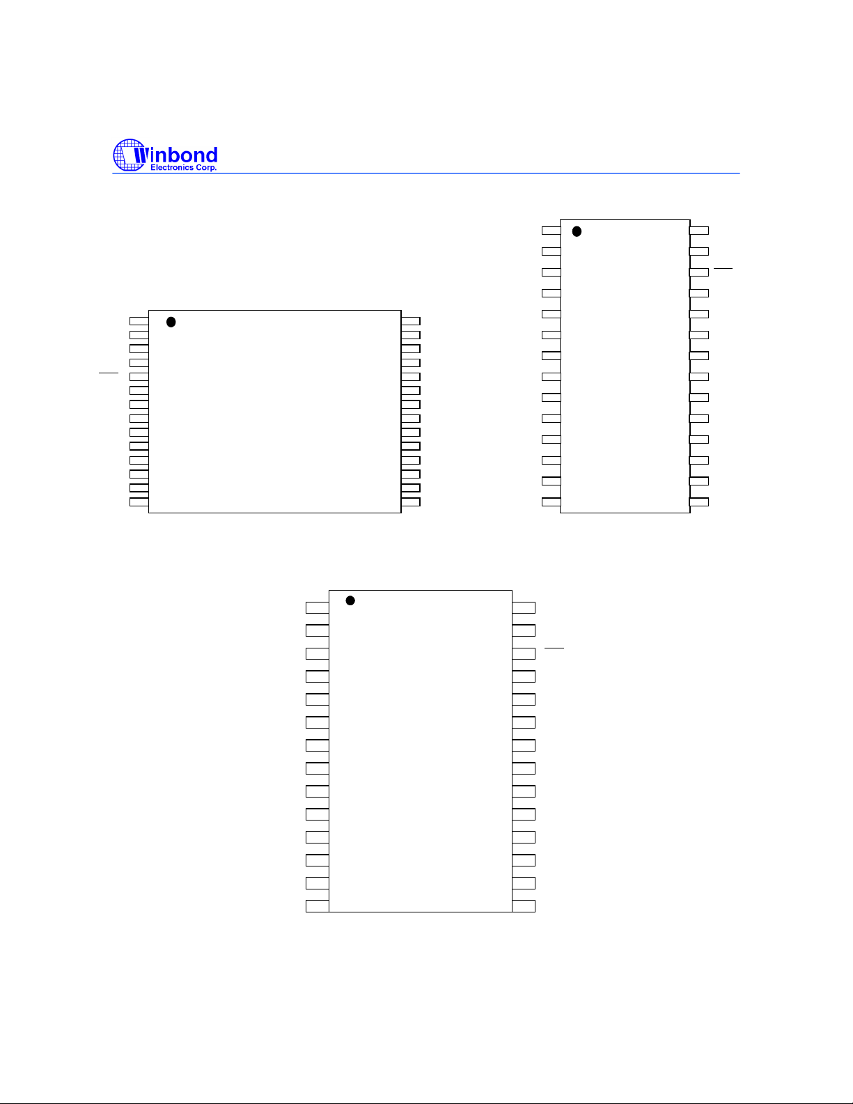
28 -PIN TSOP PDIP/SOIC
28 -PIN TSOP
PDIP
V
CCD
SCL
A1
SDA
V
SSD
V
SSD
A0
MICBS
MICMIC+
V
SSA
ACAP
SP-
V
SSA
1
2
3
4
5
6
7
8
9
10
11
12
13
14
I5216
28
27
26
25
24
23
22
21
20
19
18
17
16
15
V
CCD
MCLK
INT
RAC
SDIO
V
SSA
SDI
NC
AUX OUT
SCK
WS
AUX IN
V
CCA
SP+
SOIC
Publication Release Date: November 30, 2001
-4 Revision A1

PIN DESCRIPTION
I5216 SERIES
Advanced Information
PRELIMINARY
Pin Name Pin No.
28-pin
TSOP
RAC 4 25 25 Row Address Clock; an open drain output. The RAC pin goes LO W
Pin No.
28-pin
PDIP
Pin No.
28-pin
SOIC
Functionality
1
T
before the end of each row of m emory, and returns HIGH
RACLO
at exactly the end of each row of memory.
/INT 5 26 26 Interrupt Output; an open drain output indicating that a set EOM bit
has been found during Playback, or that the chip is in an Overflow
(OVF) condition. This pin remains LOW until a Read Status
command is executed.
MCLK 6 27 27 This pin allows the internal clock of the Voice record/playback
system to be externally driven for enhanced timing precision. T his
pin is grounded for mos t applications. It is required for the CODEC
operation.
SCL 9 2 2 Serial Clock Line is part of the I2C serial bus. It is used to clock the
data into and out of the I
2
C interface.
SDA 11 4 4 Serial Data Line is part of the I2C serial bus. Data is passed
between devices on the bus over this line.
A0 12 5 7 Input pin that supplies the LSB for the I2C Slave Address.
A1 10 3 3 Input pin that supplies the LSB +1 bit for the I2C Slave Address.
MIC+ 16 9 10 Differential positive Input to the microphone amplifier.
MIC- 17 10 9 Differential negative Input to the microphone amplifier.
MICBS 18 11 8 Microphone Bias Voltage
ACAP 19 12 12 AGC Capacitor connection. Required for the on-chip AGC amplifier.
SP+ 22 15 15 Differential Positive Speaker Driver Output.
SP- 20 13 13 Differential Negative Speaker Driver Output. When the speaker
outputs are in use, the AUX OUT output is disabled.
AUX IN 24 17 17 Auxiliary Input. This is one of the gain adjustable analog inputs for
the device.
AUX OUT 25 18 20 Auxiliary Output. This is one the analog outputs for the device.
When this output is in use, the SP+ and SP- outputs are disabled.
SDI 2 23 22 Serial Digital Audio PCM Input.
SDIO 3 24 24 Serial Digital Audio PCM Output or I2S Input/Output.
WS 28 21 18 Digital audio PCM Frame sync (FS) or I2S Word Sync (WS).
SCK 27 20 19 Digital audio PCM or I2S Serial Clock.
V
7,8 1,28 1,28 Positive Digital Supply pins. These pins carry noise generated by
CCD
internal clocks in the chip. They must be carefully bypassed to
Digital Ground to ensure correct device operation.
V
13,14 6,7 5,6 Digital Ground pins.
SSD
V
1,15,21 8,14,22 11,14,23 Analog Ground pins.
SSA
V
23 16 16 Positive Analog Supply pin. This pin supplies the low level audio
CCA
sections for the device. It should be carefully bypassed to Analog
Ground to ensure correct device operation.
NC 26 19 21 No Connection
1
See parameters section of the datasheet.
Publication Release Date: November 30, 2001
-5 Revision A1
BLOCK DIAGRAMS
I5216 SERIES
Advanced Information
PRELIMINARY
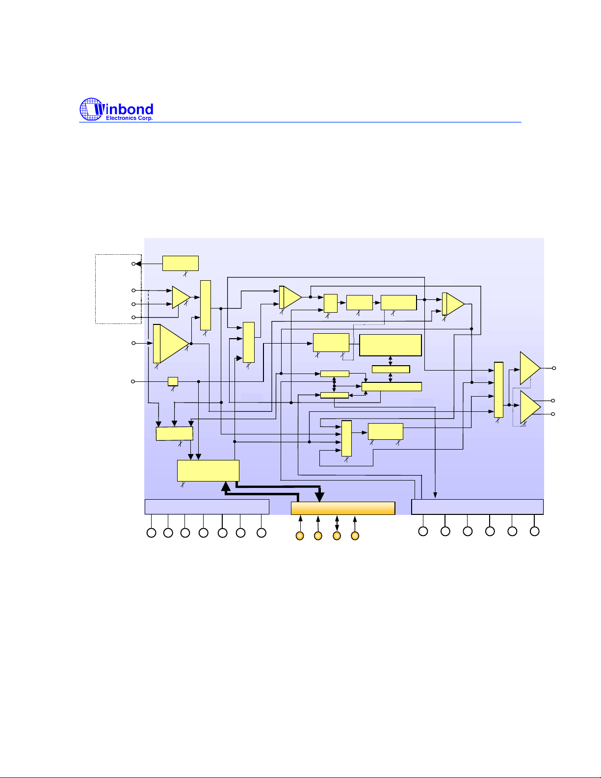
I5216 Block Diagram
MICBS
MICROPHONE
MIC+
MIC -
AGCCAP
AUX IN
MCLK
2.2V Voltage
reference
(AGPD)
AGC
(AGPD)
AUX IN
1.0 / 1.4 / 2.0 / 2.8
AUX IN
AMP
(AXPD)
AXG0
( )
2
AXG1
÷2
(CKD2)
MIC+
1
MIC-
INP
SUM2
C
E
O
D
C
u
x
M
CDI0
2
( )
CDI1
ADPD
2
( )
DAPD
Power Conditioni ng
V
V
CCA
V
SSA
1
Input Source MUX
MIC IN
1
1
(INS0)
1
µµµµ-Law / A-Law /
Linear 14 bit
CODEC
SSAVSSD
V
FILTO
ARRAY
SSD
DAO
SUM1 MUX
S1S0
( )
S1S1
ARRAY OUT
(ANALOG)
V
CCD
SUM1 MUX
( )
2
V
CCD
INP
S1M0
S1M1
SUM1
Summing
AMP
ΣΣΣΣ
SUM1
ARRAY
2
Internal
Clock
OSPD
( )
2
CKDV
( )
SUM2
(ANALOG)
2 x 64 S/H
CTRL
(DIGITAL)
2 x 64-bit reg.
SUM1
DAO
SUM2
PCM / I2S Interface
WS SCK SDIO SDI
MUX
FLD0
FLD1
INP
Filter
(FLS0)
1
Auto mute
Auto gain
1
(AMT0)
Storage Array
2
A/D
Program/Read Control
Vol MUX
VLS0
( )
VLS1
2
Low Pass
Filter
1
Multilevel
Array I/O Mux
Volume
Control
(VLPD)
1
(FLPD)
( )
3
ARRAY OUT
(DIGITAL)
VOL0
VOL1
VOL2
SCL
SUM1
FILTO
AUX IN
SUM2
Summing
AMP
ΣΣΣΣ
S2M0
( )
2
S2M1
FILTO
SUM2
VOL
DAO
Device Control
RACINTSDA
Output MUX
2
OPS0
( )
OPS1
AUX
OUT
AMP
Spkr.
AMP
2
OPA0
( )
OPA1
A1A0
AUX OUT
SPEAKER
SP+
SP-
5/22/01
Publication Release Date: November 30, 2001
-6 Revision A1
I5216 SERIES
(
)
Advanced Information
PRELIMINARY
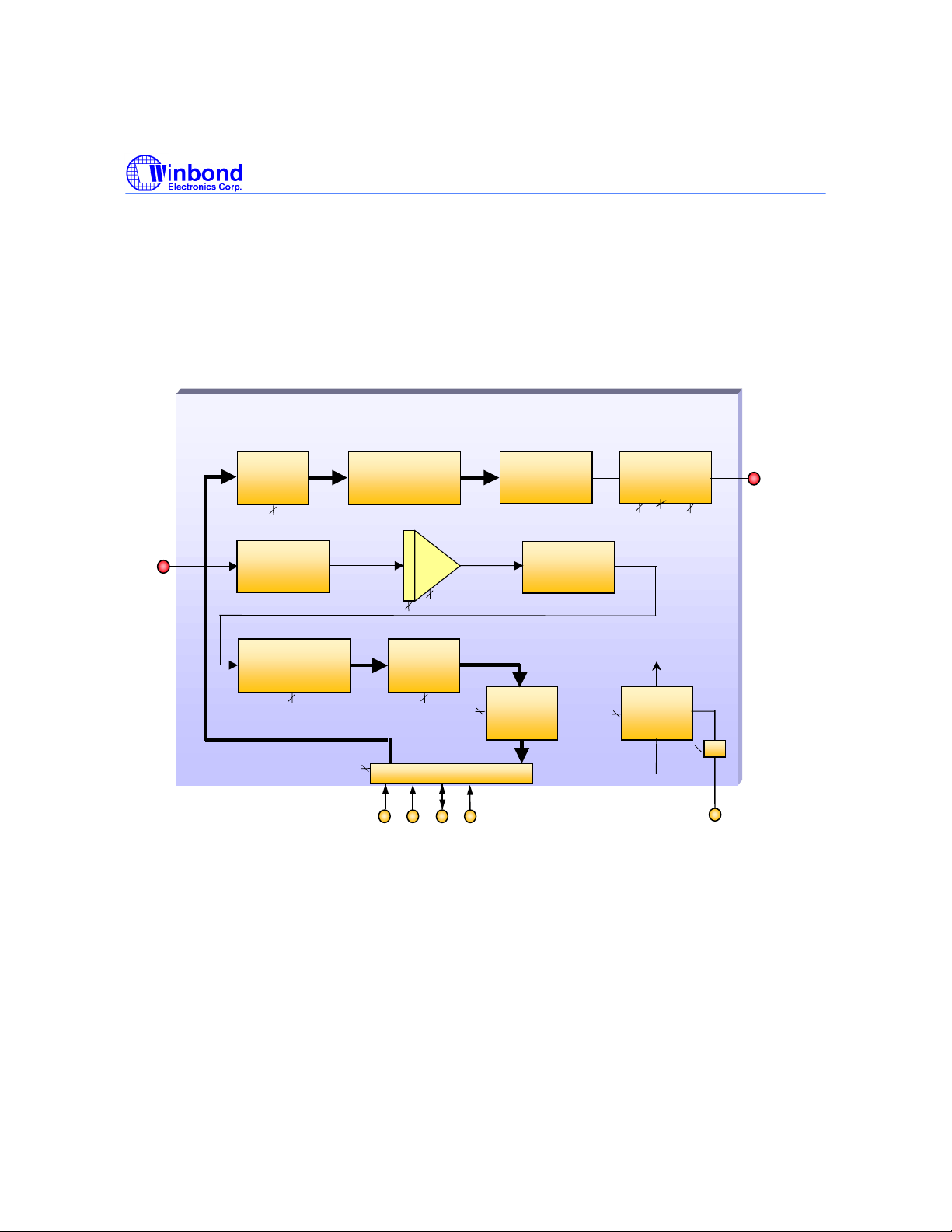
I5216 CODEC DIA G RAM
ANALOG IN
5/8/01
µ/A-Law
Expander
or linear
LAW0
2
LAW1
( )
Anti
Aliasing
Filter
Digital
Anti-Aliasing
Decimation Filter
MUTE
( )
1
1
8 bits or 16
bits
14 bit
Interpolation Filter
CIG0
CIG1
( )
CIG2
15 bit
1
I2S0
( )
Digital
Smoothing
0.8/1/1.2/1.25/1.4/1.6/1.8/2
SC
AMP
(ADPD)
1
3
Digital
High pass
Filter
HPF0
( )
WS SCK SDIO SDI
2
HSR0
( )
PCM / I2S Interface
LAW0
LAW1
14 bit
14 bit
2
Digital
Σ∆
Demodulator
Modulator
µ/A-Law
Compressor
or linear
8 bits or 16
bits
Analog
Σ∆
1 bit
HSR0
( )
MUTE
( )
1 bit D/A
& SC
Filter
1
1
DAPD
1 bit
Sample frequency
Digital
1
PLL
WS
CKD2
( )
3
COG0
COG1
( )
COG2
1
÷2
MCLK
DAO
ANALOG OUT
Publication Release Date: November 30, 2001
-7 Revision A1

I5216 SERIES
Advanced Information
PRELIMINARY
FUNCTIONAL DESCRIPTION
The I5216 ChipCorder Product provides high quality, fully integrated, single-chip Record/Playback
solutions for 8- to 16-m inute messaging applications that are ideal for use in PBX systems, cellular
phones, automotive communications, GPS/navigation systems, and other portable products. The I5216
product is an enhancement to the ISD5116 arc hitecture, providing: 1) A f ull duplex Voice CODEC with
µ-Law and A-Law compander, with I
reduced noise coupling. This supply can also be used to power down the external m icrophone with the
system.
Analog functions and audio gating have also been integrated into the I5216 product to allow for easy
interfacing with integrated chip sets on the market. Audio paths have been designed to enable full
duplex conversation record, voice memo and answering machine (including outgoing message
playback).
Logic Interface Options of 2.0V and 3.0V ar e supported by the I5216 to accomm odate both portable
communication (2.0- and 3.0-volt required) and automotive product customers (5.0-volt required).
Like other ChipCorder
filters, and multi-level storage array on a single chip. For enhanced voice features, the I5216 eliminates
external circuitry by integrating automatic gain control (AGC), a power am plif ier/speak er driver, volum e
control, summing am plifiers, analog switches, and a Voice CODEC. Input level adjustable am plifiers
are also included, providing a flexible interface for multiple applications.
Recordings are stored in on-chip nonvolatile m emory cells, providing zero-power message storage.
This unique, single-chip solution is made possible through Winbond’s patented multilevel storage
technology. Voice and audio signals are stored directly into solid-state memory in their natural,
uncompressed form, providing superior quality voice and music reproduction.
products, the I5216 integrates the sam pling clock, anti-aliasing and sm oothing
2
S and PCM interface ports; 2) A 2.2V m icrophone bias supply for
SPEECH/SOUND QUALITY
The I5216 ChipCorder product can be configured, via software, to operate at 4.0, 5.3, 6.4, and 8.0 kHz
sampling frequencies, allowing the user a choice of speech quality options. Increasing the duration
decreases the sampling frequency and bandwidth, which affects sound quality. The "Input Sample
Duration" table below compares filter pass band and product durations.
DURATION
To meet end-system r equirements, the I5216 device is a single-c hip solution, which provides 8 to 16
minutes of voice record and playback, depending on the sample rates defined by the customer's
software.
INPUT SAMPLE RATE TO DURATION INPUT SAMPLE
Rate (kHz) Duration
(Minutes)
8.0 8 min 3 sec 3.7
6.4 10 min 4 sec 2.9
5.3 12 min 9 sec 2.5
4.0 16 min 6 sec 1.8
1. Minus any pages selected for digital storage
1
Typical Filter Pass Band (kHz)
Publication Release Date: November 30, 2001
-8 Revision A1

I5216 SERIES
Advanced Information
PRELIMINARY
FLASH STORAGE
One of the benefits of W inbond’s ChipCorder technology is the use of on-chip nonvolatile memory,
which provides zero-power message storage. A message is retained for up to 100 years (typically)
without power. In addition, the device can be re-recorded over 10,000 times (typically) for digital
messages and over 100,000 times (typically) for analog messages.
A new feature has been added that allows for the allocation of m emory space in the I5216, to either
digital or analog storage, when recording. When m ak ing a recording, if a section is assigned for digital
or analog data storage, the system microcontroller stores this information in the Message Address
Table.
MICROCONTROLLER INTERFACE
The I5216 is controlled through an I2C 2-wire interface. This synchronous serial port allows commands,
configurations, address data, and digital data to be loaded to the device, while allowing status, digital
data and current address information to be read back from the device. In addition to the serial
interface, two other pins can be connected to the microcontroller for enhanced interface: the RAC
timing pin and the INT\ pin for interrupts to the controller. Communications with all of the internal
registers is through the serial bus, as well as digital memory Read and Write operations.
PROGRAMMING
The I5216 series is also ideal for playback-only applications, whereas single or m ultiple messages may
be played back when desired. Playback is controlled through the I
configuration is created, duplicates can easily be generated via a W inbond or third-party program mer.
For more inform ation on available application tools and programmers , please see the Winbond web
site at http://www.winbond-usa.com/
.
2
C port. Once the desired m essage
APPLICATIONS
The I5216 is a single chip solution for voice and analog storage that also includes the capability to
store digital information in the m emory array. T he array may be divided between analog and digital
storage, as the user chooses, when configuring the device.
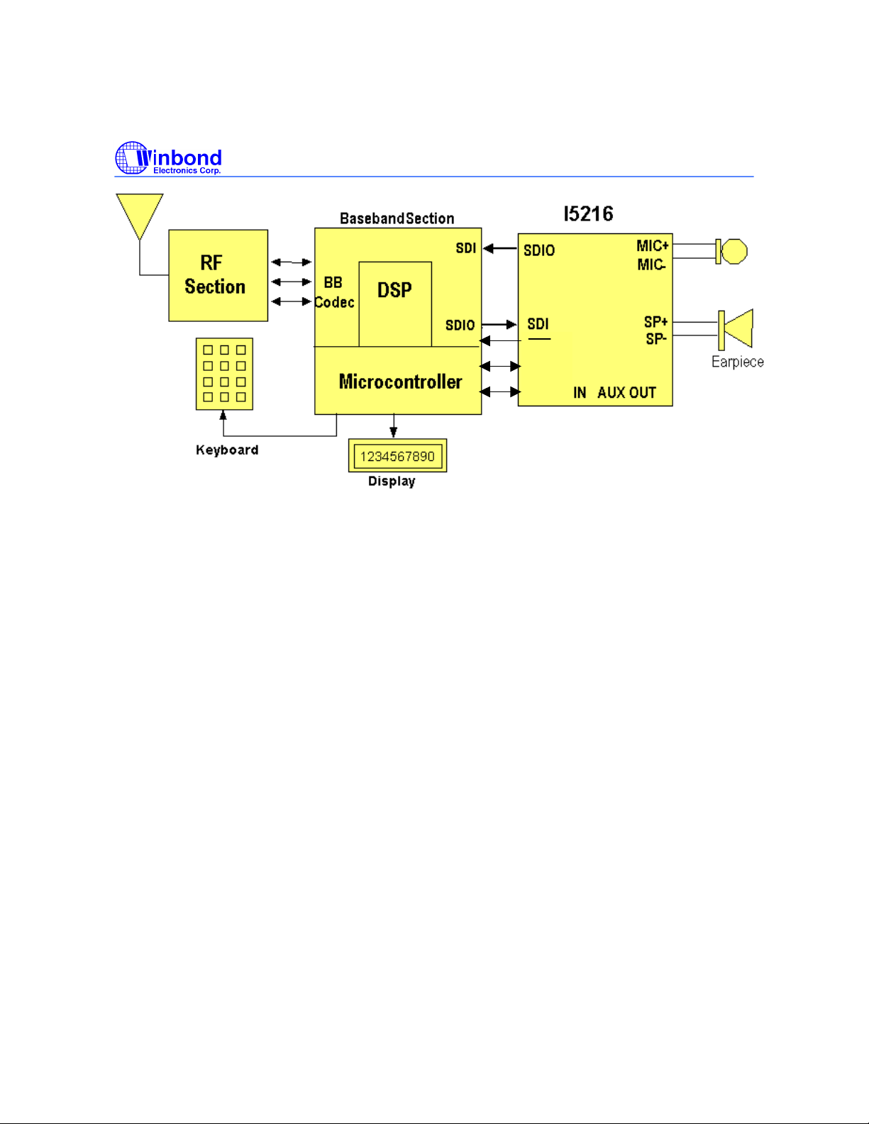
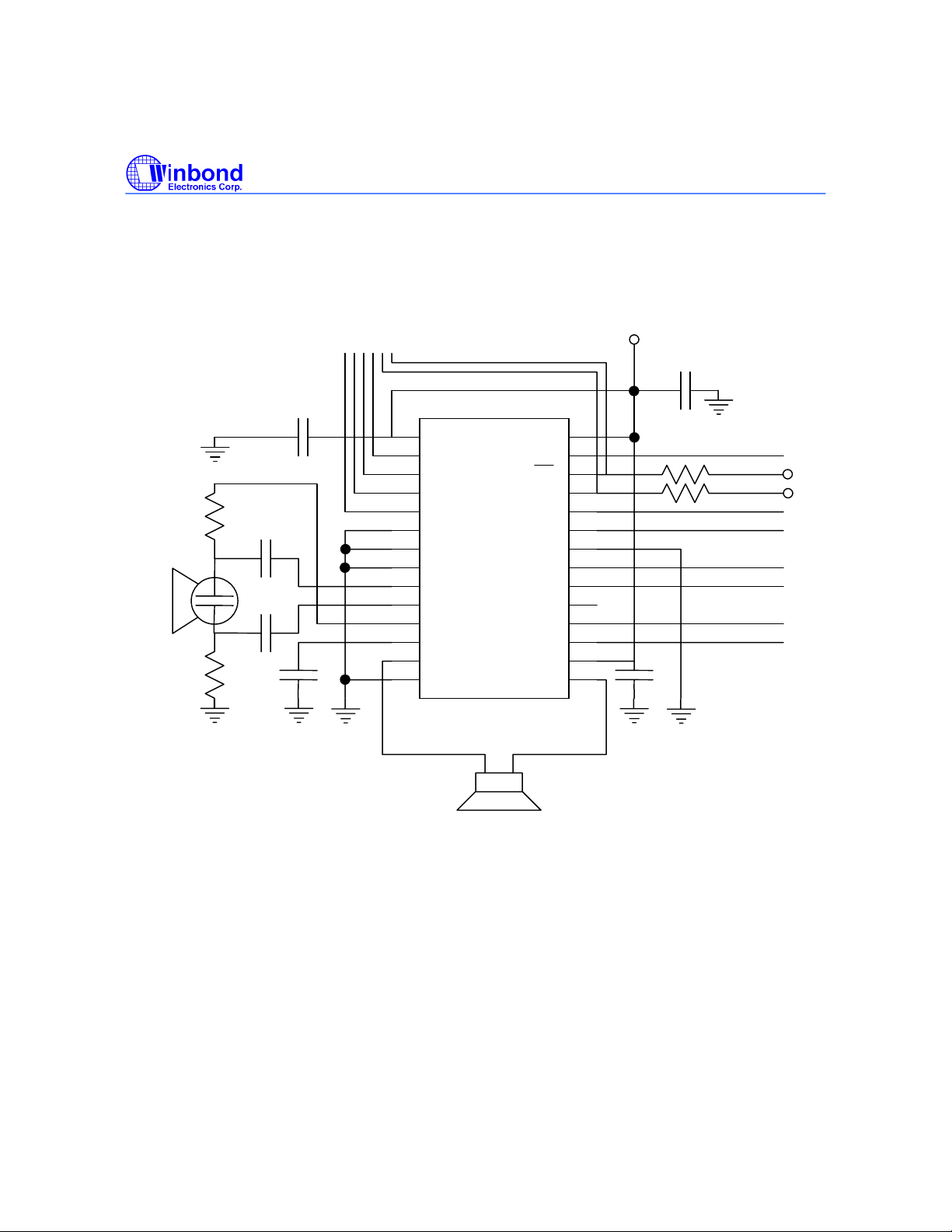
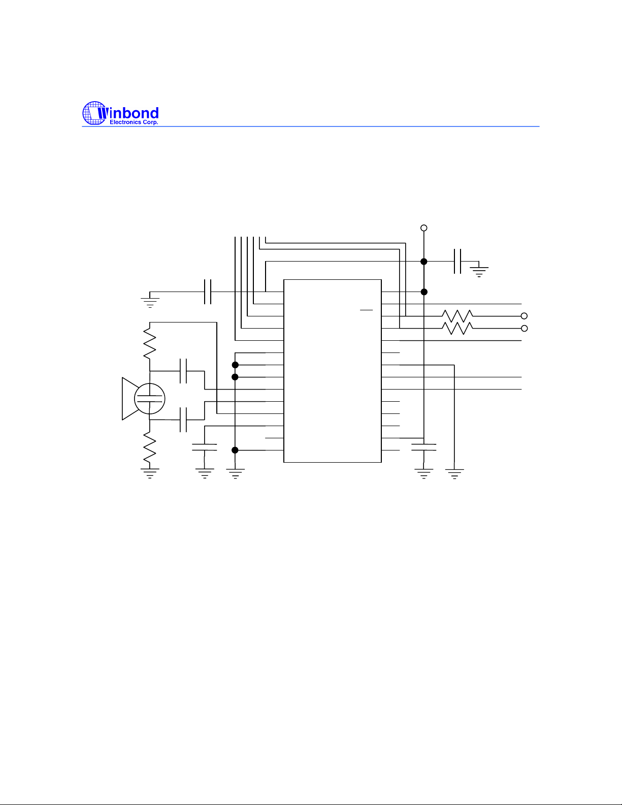
Looking at the block diagram on the following page, one can see that the I5216 may be very easily
designed into a cellular phone. Placing the device between the microphone and the exis ting baseband
chip takes care of the transmit path. The SDI/SDIO of the baseband chip is connected to the SDIO/SDI
of the I5216. Two pins are needed for the I
2
C digital control and digital information for storage.
Publication Release Date: November 30, 2001
-9 Revision A1
I5216 SERIES
Advanced Information
PRELIMINARY
INT
SCL
SDA
Starting at the MICROPHONE inputs, the input signal at the MICROPHONE inputs c an be routed in
the following ways:
• directly through the Voice band CODEC of the I5216 chip, then through the SDIO pin, to output
the digital PCM signal.
• through the AGC amplifier, before it is routed to the voice band CODEC.
• through the AGC amplifier to the storage array
• through the AGC amplifier and mixed with an analog voice band CODEC signal c oming from
the digital SDI pin
In addition, if the phone is inserted into a "hands-free" car kit, then the signal from the pickup
microphone in the car can be passed through to the s ame places from the AUX IN pin and the phone's
microphone is switched off. In this s cenario, the other party's voice from the phone would be played
into the PCM IN input and passed through to the AUX OUT pin that would drive the car kit's
loudspeaker.
Depending upon whether one desires recording one side (simplex) or both sides (duplex) of a
conversation, the various paths will also be switched through to the low pass filter (for antialiasing) and
into the storage array. Later, the cell phone owner can play back the messages from the array. When
this happens, the Array Output MUX is connected to the volume control, through the Output MUX, to
the Speaker Amplifier. For applications other than a cell phone, the audio paths can be s witched into
many different and flexible configurations. Some examples follow.
Publication Release Date: November 30, 2001
-10 Revision A1

A
A
A
A
5
µ
A
Electret Microphone
WM-54B Panasonic
1.5kΩ
1.5kΩ
.1
.1µF
.1µF
F
To Microcontroller
2
C interface and
I
ddress setting
1µF
TRANSFORMER APPLICATION
V
3
4
5
6
7
8
9
10
12
14
600Ω
CCD
SCL
1
SDA
0
V
SSD
V
SSD
V
SSA
MIC+
MICMICBS
CAP
SPV
SSA
600Ω
AUX OUT
=
=
V
CCD
MCLK
INT
RAC
SDIO
SDI
V
SSA
WS
SCK
NC
AUX IN
V
CC
SP+
27
26
25
24
23
22
21
20
19
18
17
1
I5216 SERIES
Advanced Information
PRELIMINARY
Vcc
.1µF
4.7KΩ
.1µF
Vcc
Vcc
PCM OUT
PCM IN
8 KHz
2.048 MHz
.1µF
Publication Release Date: November 30, 2001
-11 Revision A1
I5216 SERIES
A
A
A
9
µ
A
g
Advanced Information
PRELIMINARY
Electret Microphone
WM-54B Panasonic
HANDSET APPLICATION
.1µF
1.5kΩ
.1µF
F
.1
1.5kΩ
To Microcontroller
I
.1µF
2
C interface and
ddress settin
1
2
3
4
5
6
7
8
9
10
11
12
13
14
V
CCD
SCL
1
SDA
0
V
SSD
V
SSD
V
SSA
MIC+
MICMICBS
CAP
SP
V
SSA
Vcc
.1µF
AUX OUT
AUX IN
V
CCD
MCLK
RAC
SDIO
SDI
V
SSA
SCK
NC
V
CCA
SP+
28
27
26
25
24
23
22
21
1
18
17
16
15
.1µF
4.7KΩ
4.7KΩ
13.824 MHz
Vcc
Vcc
PCM OUT
PCM IN
8 KHz
2.048 MHz
TO RINGER
Publication Release Date: November 30, 2001
-12 Revision A1
A
A
A
318
A
g
S S
/O
3.0
ccVccVcc
Electret Microphone
WM-54B Panasonic
1.5kΩ
1.5kΩ
.1µF
.1µF
.1µF
1µF
CAR STEREO APPLICATION
To Microcontroller
2
C interface and
I
ddress settin
1
V
2
3
4
5
7
8
10
11
12
13
14
CCD
SCL
1
SDA
0
6
V
SSD
V
SSD
V
SSA
9
MIC+
MICMICBS
CAP
SP-
SSA
V
CCD
MCLK
INT
RAC
SDIO
SDI
V
SSA
WS
SCK
NC
AUX OUT
AUX IN
V
CCA
SP+V
I5216 SERIES
Advanced Information
PRELIMINARY
V
.1µF
4.7KΩ
4.7KΩ
24
2
17
.1µF
20.48 MHz
2
I
ERIAL I
48 KHz
72 MHz
Publication Release Date: November 30, 2001
-13 Revision A1
I5216 SERIES
Advanced Information
PRELIMINARY
INTERNAL REGISTERS
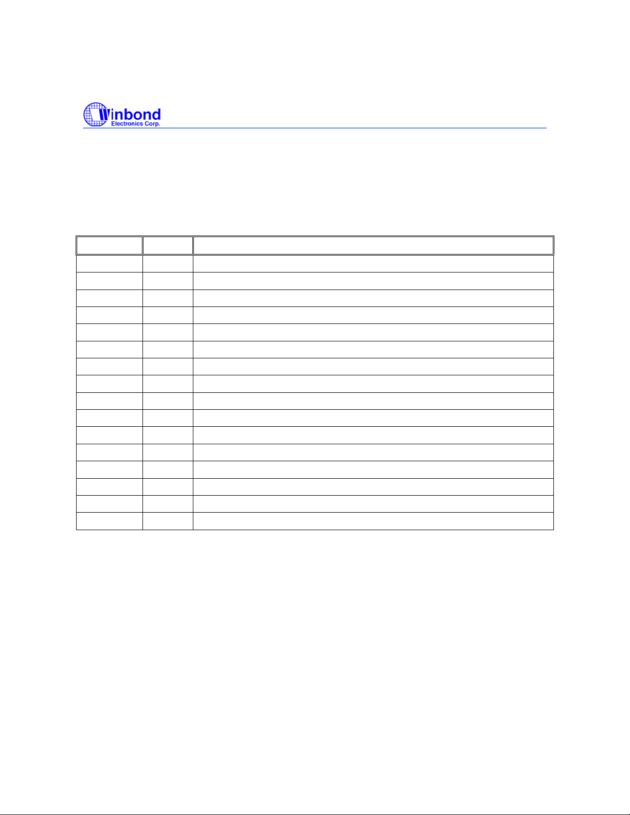
The following tables provide a general illustration of the bits. T here are three configuration registers:
CFG0, CFG1 and CFG2. Thus, there are six 8-bit bytes to be loaded during the set-up of the device.
CFG0
Bit no. Signal Description
D0 (LSB) VLPD Power down the Volume Control.
D1 OPA0 Power down Speaker driver and/or Auxiliary output.
D2 OPA1 Power down Speaker driver and/or Auxiliary output.
D3 OPS0 Select speaker output multiplexer.
D4 OPS1 Select speaker output multiplexer.
D5 CDI0 Analog to digital converter input selector.
D6 CDI1 Analog to digital converter input selector.
D7 AMT0 Compress the filter signal.
D8 OSPD Power down the internal ChipCorder oscillator.
D9 INS0 Select Microphone input or Auxiliary input.
D10 AXPD Power down Auxiliary input amplifier.
D11 AXG0 Auxiliary input amplifier gain setting.
D12 AXG1 Auxiliary input amplifier gain setting.
D13 CIG0 Input gain setting for the Analog to digital converter.
D14 CIG1 Input gain setting for the Analog to digital converter.
D15 (MSB) CIG2 Input gain setting for the Analog to digital converter.
Publication Release Date: November 30, 2001
-14 Revision A1

PRELIMINARY
CFG1
Bit no. Signal Description
D0 (LSB) AGPD Power down the Microphone AGC
D1 FLPD Power down the Filter
D2 FLD0 Set the duration and sample rate of the ChipCorder
D3 FLD1 Set the duration and sample rate of the ChipCorder
D4 FLS0 Select the filter input signal
D5 S2M0 Select Sum Amplifier 2 input
D6 S2M1 Select Sum Amplifier 2 input
D7 S1M0 Select Sum Amplifier 1 input
D8 S1M1 Select Sum Amplifier 1 input
D9 S1S0 Select Sum Amplifier 1 multiplexer
D10 S1S1 Select Sum Amplifier 1 multiplexer
D11 VOL0 Volume Control Setting
D12 VOL1 Volume Control Setting
D13 VOL2 Volume Control Setting
D14 VLS0 Select Volume Control input
D15 (MSB) VLS1 Select Volume Control input
I5216 SERIES
Advanced Information
Publication Release Date: November 30, 2001
-15 Revision A1

I5216 SERIES
Advanced Information
PRELIMINARY
CFG2
Bit no. Signal Description
D0 (LSB) ADPD Power down the Analog to Digital converter
D1 DAPD Power down the Digital to Analog converter
D2 LAW0
D3 LAW1
D4 I2S0 Select the I2S interface
D5 HSR0 Enable the high sample rate mode
D6 HPF0 Enable High Pass Filter
D7 MUTE Mute the CODEC A/D and D/A path
D8 CKDV Divide MCLK by 2560 or 1728 for 8 kHz ChipCorder sample rate
D9 COG0 Output gain setting for the Digital to Analog converter
D10 COG1 Output gain setting for the Digital to Analog converter
D11 COG2 Output gain setting for the Digital to Analog converter
D12 CKD2 Divide MCLK frequency by 2 or 1
D13 - Reserved
D14 - Reserved
D15 (MSB) - Reserved
Select digital µ-Law or A-Law input/output format
Select digital µ-Law or A-Law input/output format
Publication Release Date: November 30, 2001
-16 Revision A1

I5216 SERIES
Advanced Information
PRELIMINARY
MEMORY ORGANIZATION
The I5216 memory array is arranged as 1888 rows (or pages) of 2048 bits, for a total memory of
3,866,624 bits. The primary addressing for the 2048 pages is handled by 11 bits of address data in the
analog mode. At the 8 kHz sample r ate, each page contains 256 m illisec onds of audio. T hus , at 8 k Hz
there is actually room for 8 minutes and 3 seconds of audio.
A memory page is 2048 bits organized as thirty-two 64-bit "blocks " when used f or digital s tor age. The
contents of a page are either analog or digital. T his is determined by instruction (op code) at the time
the data is written. A record of what is analog and what is digital, and where, is stored by the system
microcontroller in the m essage address table (MAT). The MAT is a table kept in the microcontroller
memory that defines the status of each message “block.” It can be s tored back into the I5216 if the
power fails or the system is turned of f. Use of this table allows for efficient message managem ent.
Segments of messages can be stored wherever there is available space in the m emory array. [This
is explained in detail for the Winbond I5008 in Applications Note #No.9 and will similar ly be in a later
Note for the I5216.]
When a page is used for analog stor age, the same 32 block s are pres ent, but there are 8 EOM (Endof-Message) m arkers. This means that for each 4 blocks there is an EOM marker at the end. Thus,
when recording, the analog recording will stop at any one of eight positions. At 8 kHz, this results in a
resolution of 32 msec when ENDING an analog recording. Beginning an analog recor ding is limited to
the 256 msec resolution provided by the 11-bit address. A recording does not imm ediately stop when
the Stop command is issued, but continues until the 32-m illisecond block is filled. T hen a bit is placed
into the EOM memory to develop the interrupt that signals a message is finished playing in the
Playback mode.
2
Digital data is sent and received, serially, over the I
and stored in one of two alternating (commutating) 64- bit shift register s. W hen an input register is full,
it becomes the register that is par allel written into the array. The prior write register becom es the new
serial input register. A mechanis m is built in to ensure there is always a register available for s toring
new data.
Storing data in the memory is accomplished by accepting data, one byte at a time, and issuing an
acknowledgement. If data is coming in faster than it can be written, then the chip will not issue an
acknowledgement to the host microcontroller until it is ready.
The read mode is the opposite of the write m ode. Data is r ead into one of two 64-bit regis ters f rom the
array and serially sent to the I
2
C port. (See Digital Mode on page 41 for details).
C interface. The data is ser ial-to-parallel c onverted
OPERATION MODES DESCRIPTION
I2C PORT
Important note: The content contained herein of the r est of t his datasheet assum es t hat the
reader is familiar with the I
2
C section of this document. If you are not familiar with this serial prot ocol, please read
the I
the I2C section to familiarize yourself with it. A significant amount of additional information on
2
C can also be found on the Philips web page at http://www.philips.com/.
I
2
C serial interface. Additional informat ion on I2C may be found in
Publication Release Date: November 30, 2001
-17 Revision A1

I5216 SERIES
Advanced Information
PRELIMINARY
I2C SLAVE ADDRESS
The I5216 has a 7 bit slave address of <100 00xy> where x and y are equal to the state, respectively,
of the external address pins A1 and A0. Because all data bytes are required to be 8 bits, the LSB of the
address byte is the Read/Write selection bit that tells the slave whether to transmit or receive data.
Therefore, there are eight possible slave addresses for the I5216
A1 A0 Slave Address R/W\
Bit
0 0 <100 00 00> 0 80
0 1 <100 00 01> 0 82
1 0 <100 00 10> 0 84
1 1 <100 00 11> 0 86
0 0 <100 00 00> 1 81
0 1 <100 00 01> 1 83
1 0 <100 00 10> 1 85
1 1 <100 00 11> 1 87
To use more than four I5216 devices in an application requires some external switching of the I
HEX Value
2
C link.
Publication Release Date: November 30, 2001
-18 Revision A1
I5216 SERIES
e
A
A
A
R
A
A
A
Advanced Information
PRELIMINARY
I2C OPERATION DEFINTIONS
There are many control functions used to operate the I5216. Among them are the following.
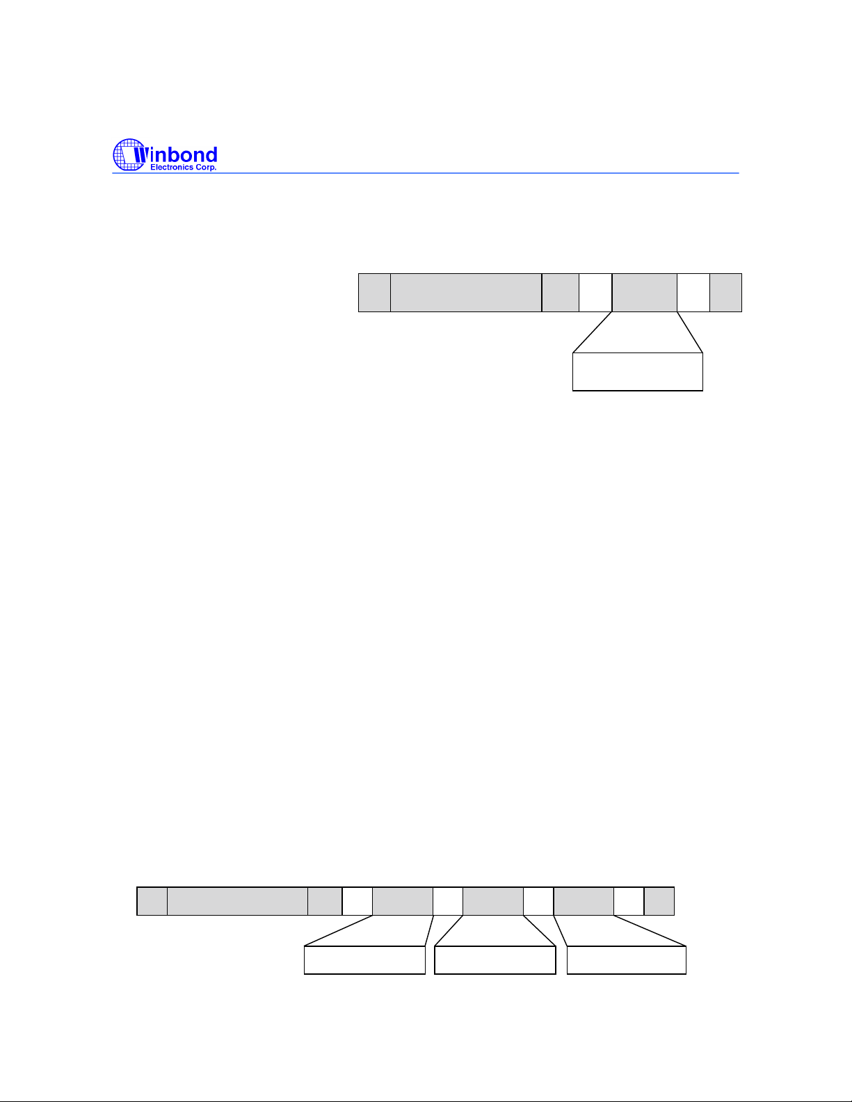
READ STATUS COMMAND: The read status command is a read
request from the Host processor to the I5216 without delivering a
Command Byte. The Host supplies all of the clocks (SCL). In each
case, the entity sending the data drives the data line (SDA). The Read
Status Command is executed by the following I
1. Host executes I
2. Send Slave Address with R/W bit = “1” (Read) 81h.
3. Slave responds back to Host an Acknowledge (ACK), followed
by 8 bit Status word.
4. Host sends an Acknowledge (ACK) to Slave.
5. Wait for SCL to go HIGH.
6. Slave responds with Upper Address byte of internal address
register.
7. Host sends an ACK to Slave.
8. Wait for SCL to go high.
9.
Slave responds with Lower Address byte of internal address
register.
10.
Host sends a NO ACK to Slave, then executes I2C STOP
Note: The processor could have sent an I2C STOP after the Status
Word data transfer, and thus aborted the transfer of the Address bytes
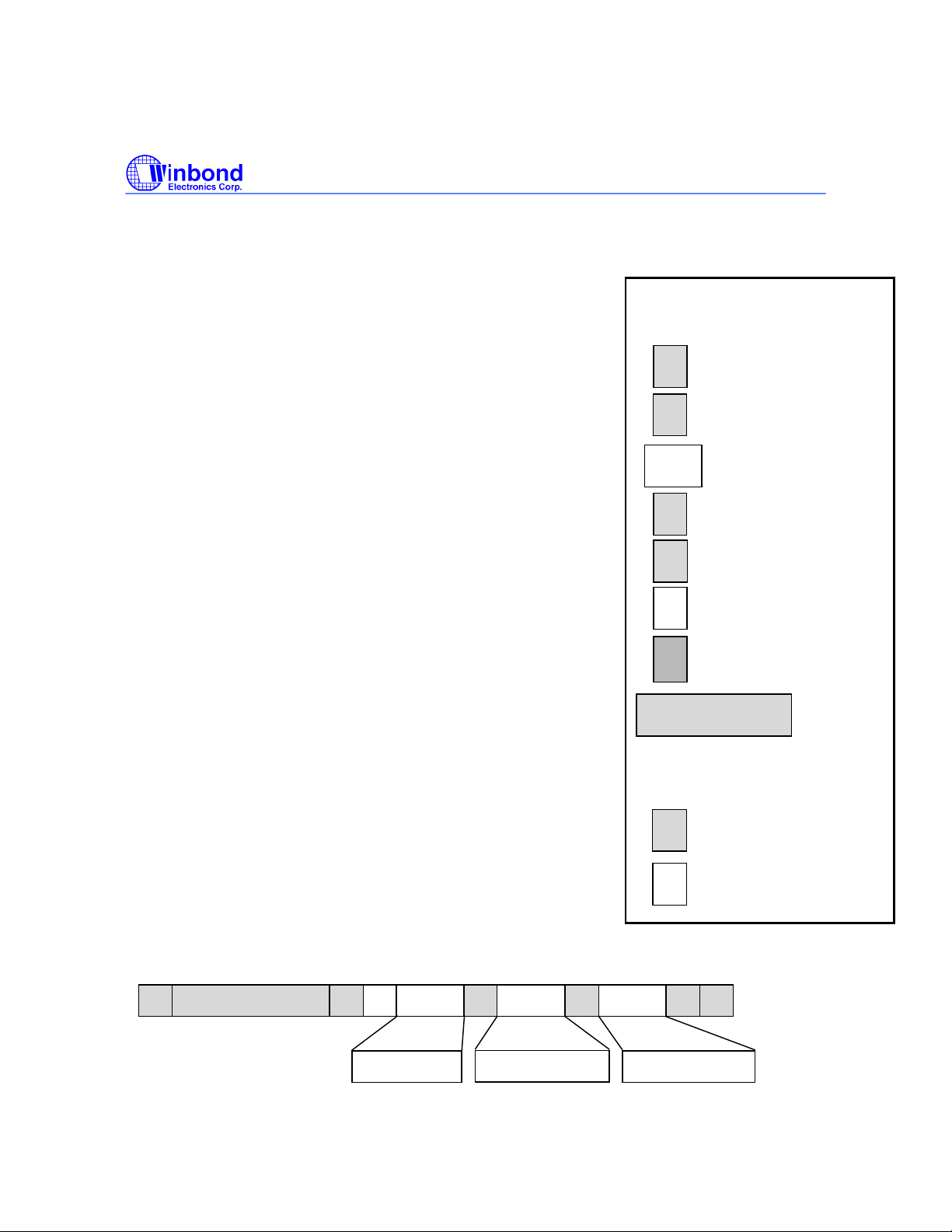
A graphical representation of this operation is found below. See the caption box above for more
explanation.
S SLAVE ADDRESS
2
C START
DAT
2
C sequence.
DAT
Conventions used in I2C Data
Transfer Diagrams
S
= START Condition
P
= STOP Condition
DATA
= 8 bit data transfer
R
= “1” in the R/W bit
W
= “0” in the R/W bit
A
= ACK (Acknowledge)
N
= No ACK
SLAVE ADDRESS
The Box color indicates the
direction of data flow
= Host to Slave (Gray)
= Slave to Host (White)
DAT
P
N
= 7 bit Slav
Address
Status
-19 Revision A1
High Addr.
Publication Release Date: November 30, 2001
Low Addr.
I5216 SERIES
A
A
A
A
A
A
Advanced Information
PRELIMINARY
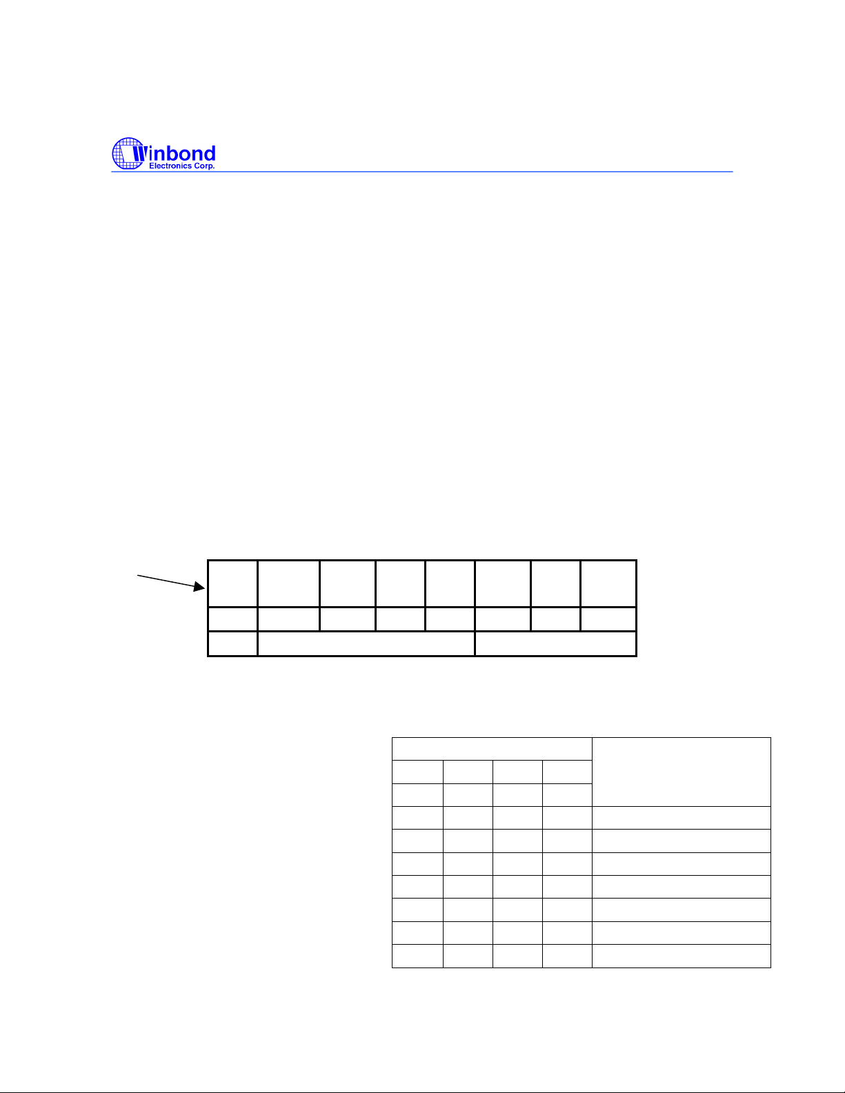
LOAD COMMAND BYTE REGISTER (Single Byte Load)
A single byte may be written to the Command Byte Register in order to power up the device, start or
stop Analog Record (if no address inform ation is needed), or perf orm a Mes sage Cueing f unction. T he
Command Byte Register is loaded as follows:
1. Host executes I2C START.
2. Send Slave Address with R/W bit = “0” (Write) [80h].
3. Slave responds back with an ACK.
4. Wait for SCL to go HIGH.
5. Host sends a command byte to Slave.
6. Slave responds with an ACK.
7. Wait for SCL to go HIGH.
8. Host executes I
2
C STOP.
S SLAVE ADDRESS A DATA
W
Command Byte
A
LOAD COMMAND BYTE REGISTER (Address Load):
For the normal addressed mode the Registers are loaded as follows:
2
1. Host executes I
2. Send Slave Address with R/W bit = “0” (Write).
3. Slave responds back with an ACK.
4. Wait for SCL to go HIGH.
5. Host sends a byte to Slave - (Command Byte).
6. Slave responds with an ACK.
7. Wait for SCL to go HIGH.
8. Host sends a byte to Slave - (High Address Byte).
9. Slave responds with an ACK.
10. Wait for SCL to go HIGH.
11. Host sends a byte to Slave - (Low Address Byte).
12. Slave responds with an ACK.
13. Wait for SCL to go HIGH.
14. Host executes I
S SLAVE ADDRESS
C START.
2
C STOP.
Command
DAT
DAT
High Addr. Low Addr.
DATA
PW
Publication Release Date: November 30, 2001
-20 Revision A1
I5216 SERIES
Advanced Information
PRELIMINARY
I2C CONTROL REGISTERS
The I5216 is controlled by loading comm ands to, or reading commands fr om the internal command,
configuration and address register s. T he Com m and byte sent is used to star t and stop r ecording, write
or read digital data and perform other functions necessary for the operation of the device.
COMMAND BYTE
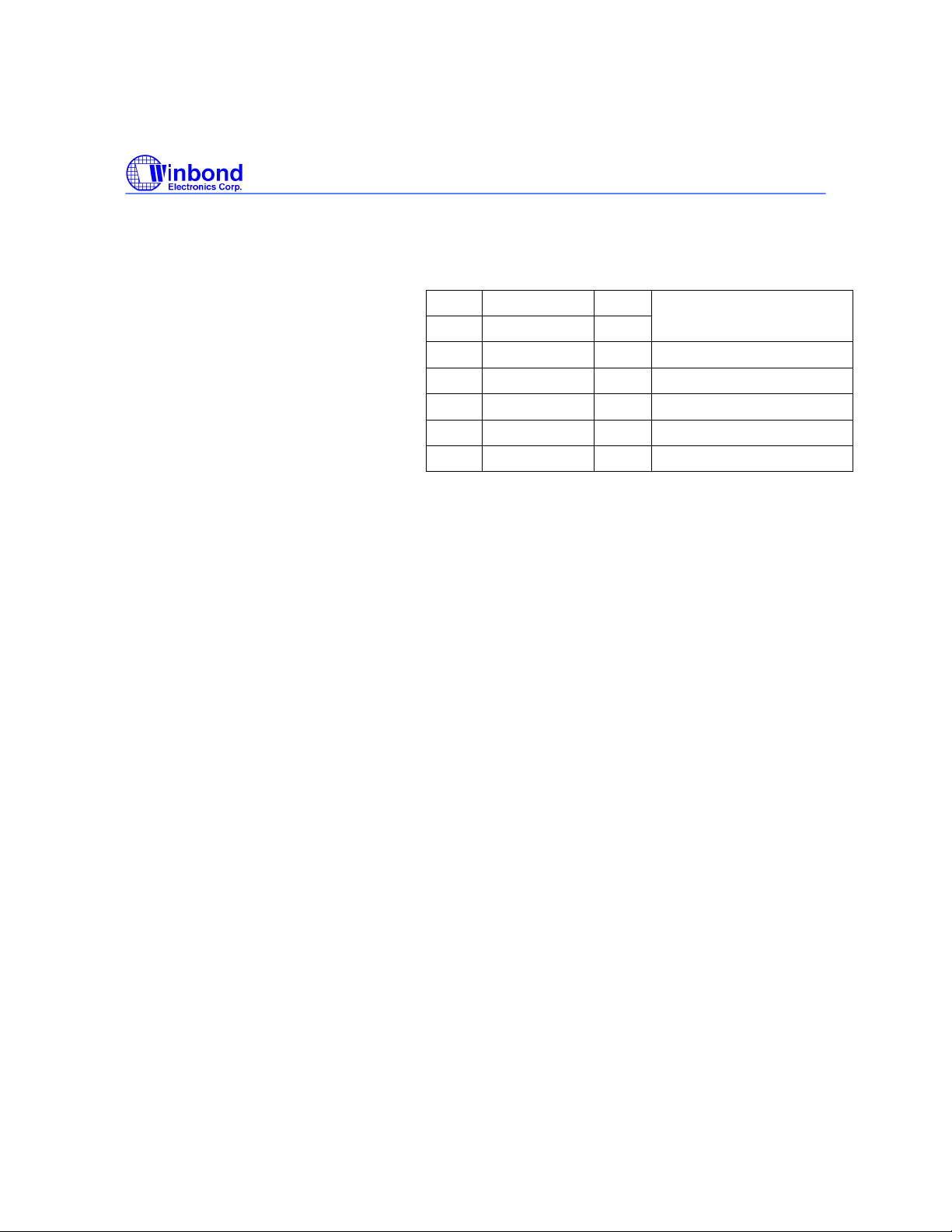
Control of the I5216 is implemented through an 8-bit com mand byte that is sent after the 7-bit device
address and the 1-bit Read/Write selection bit. The 8 bits are:
Global power up bit
DAB bit: determines whether device is performing an analog or digital function
3 func tion bits: these determ ine which function the device is to perf orm in conjunction with the
DAB bit.
3 register address bits: these determine if and when data is to be loaded to a register
Power Up Bit
C7
PU DAB FN2 FN1 FN0 RG2 RG1 RG0
Function Bits Register Bits
C6 C5 C4 C3 C2 C1 C0
FUNCTION BITS
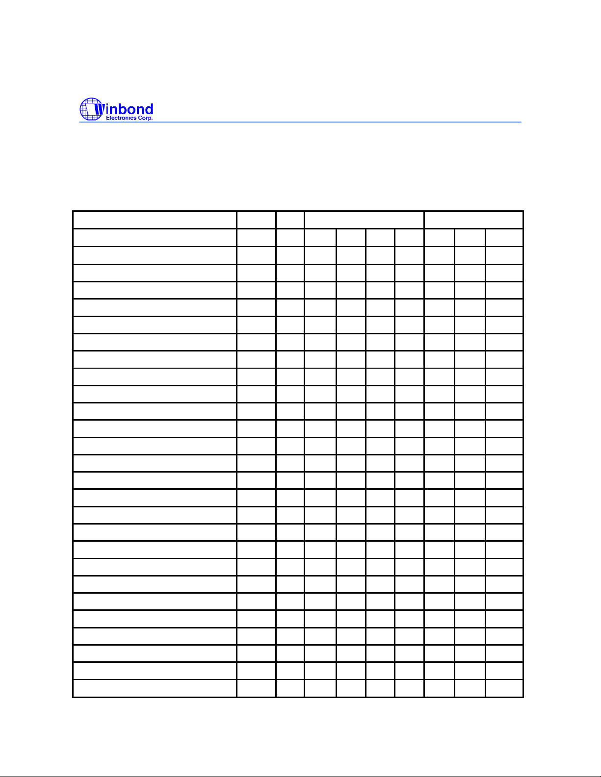
The command byte function bits are detailed
in the table to the right. C6, the DAB bit,
determines whether the device is
performing an analog or digital f unc tion. T he
other bits are decoded to produce the
individual commands. Note that not all
decode combinations are currently used;
they are reserved for future use. Out of 16
possible codes, the I5216 uses 7 f or norm al
operation. The other 9 are No Ops.
-21 Revision A1
Command Bits
C6 C5 C4 C3
DAB FN2 FN1 FN0
0 0 0 0 STOP (or do nothing)
0 1 0 1 Analog Play
0 0 1 0 Analog Record
0 1 1 1 Analog MC
1 1 0 0 Digital Read
1 0 0 1 Digital Write
1 0 1 0 Erase (row)
Publication Release Date: November 30, 2001
Function
I5216 SERIES
Advanced Information
PRELIMINARY
REGISTER BITS
The register load may be used to modify
a command sequence (such as load an
address) or used with the null command
sequence to load a configuration or test
register. Not all registers are accessible to
the user. [The remaining three codes are
No Ops.]
RG2 RG1 RG0
C2 C1 C0
0 0 0 No action
0 0 1 Load Address
0 1 0 Load CFG0
0 1 1 Load CFG1
1 0 1 Load CFG2
Function
OPCODE SUMMARY
OpCode Command Description
The following commands are used to access the chip through the I2C port:
Play: analog play command.
Record: analog record command.
Message Cue: analog message cue command.
Enter Digital mode.
Read: digital read command.
Write: digital write command.
Erase: digital page and block erase command.
Exit Digital mode.
Power up: global power up/down bit. (C7).
Load address: load address register (is incorporated in play, record, read and write
commands).
Load CFG0: load configuration register 0.
Load CFG1: load configuration register 1.
Load CFG2: load configuration register 2.
Read STAT US: Read the interrupt status and address register , including a hardwired device
ID.
Publication Release Date: November 30, 2001
-22 Revision A1
I5216 SERIES
Advanced Information
PRELIMINARY
OPCODE COMMAND BYTE TABLE
Pwr Function Bits Register Bits
OPCODE HEX PU DAB FN2 FN1 FN0 RG2 RG1 RG0
COMMAND BIT NUMBER CMD C7 C6 C5 C4 C3 C2 C1 C0
POWER UP 80 1 0 0 0 0 0 0 0
POWER DOWN 00 0 0 0 0 0 0 0 0
STOP (DO NOTHING) STAY ON 80 1 0 0 0 0 0 0 0
STOP (DO NOTHING) STAY OFF 00 0 0 0 0 0 0 0 0
LOAD ADDRESS 81 1 0 0 0 0 0 0 1
LOAD CFG0 82 1 0 0 0 0 0 1 0
LOAD CFG1 83 1 0 0 0 0 0 1 1
LOAD CFG2 85 1 0 0 0 0 1 0 1
RECORD ANALOG 90 1 0 0 1 0 0 0 0
RECORD ANALOG @ ADDR 91 1 0 0 1 0 0 0 1
PLAY ANALOG A8 1 0 1 0 1 0 0 0
PLAY ANALOG @ ADDR A9 1 0 1 0 1 0 0 1
MSG CUE ANALOG B8 1 0 1 1 1 0 0 0
MSG CUE ANALOG @ ADDR B9 1 0 1 1 1 0 0 1
ENTER DIGITAL MODE C0 1 1 0 0 0 0 0 0
ERASE DIGITAL PAGE D1 1 1 0 1 0 0 0 1
WRITE DIGITAL C8 1 1 0 0 1 0 0 0
WRITE DIGITAL @ ADDR C9 1 1 0 0 1 0 0 1
READ DIGITAL E0 1 1 1 0 0 0 0 0
READ DIGITAL @ ADDR E1 1 1 1 0 0 0 0 1
EXIT DIGITAL MODE 40 0 1 0 0 0 0 0 0
READ STATUS REGISTER
1
N/A N/A N/A N/A N/A N/A N/A N/A N/A
Publication Release Date: November 30, 2001
-23 Revision A1
I5216 SERIES
Advanced Information
PRELIMINARY
1
See Playback and Stop Cycle on page 62 for details.
DATABYTES
In the I2C write mode, the device can accept data sent after the command byte. If a register load option
is selected, the next two bytes are loaded into the selected register. The format of the data is MSB first,
as specified by the I
the byte is acknowledged, and DATA<7:0> is sent next. The address regis ter consists of two bytes.
The format of the address is as follows:
ADDRESS<15:0> = PAGE_ADDRESS<10:0>, BLOCK_ADDRESS<4:0>
If an analog function is selected, the bloc k addr ess bits m ust be s et to 00000. Digital Read and Write
are block addressable.
When the device is polled with the Read Status command, it will return three bytes of data. T he first
byte is the status byte, the next is the upper address byte and the last is the lower address byte. The
status register is one byte long and its bit function is:
STATUS<7:0> = EOM, OVF, READY, PD, PRB, DEVICE_ID<2:0>
The lower address byte will always return the block address bits as zero, either in digital or analog
mode.
The functions of the bits are:
2
C standard. Thus to load DATA<15:0> into the devic e, DATA<15:8> is sent fir st,
BIT# NAME FUNCTION
7 EOM Indicates whether an EOM interrupt has occurred.
6 OVF Indicates whether an overflow interrupt has occurred.
5 READY Indicates the internal status of the device – if READY is LOW no new
commands should be sent to device.
4 PD Device is powered down if PD is HIGH.
3 PRB Play/Record mode indicator. HIGH=Play/LOW=Record.
2
1
DEVICE_ID
0
It is good practice to read the status register after a Write or Record operation to ensure that the
device is ready to accept new commands. Depending upon the design and the number of pins
available on the controller, the polling overhead can be reduced. If INT\ and RAC are tied to the
microcontroller, the controller does not have to poll as frequently to determine the status of the I5216
An internal device ID. This is 001 for the I5216.
Publication Release Date: November 30, 2001
-24 Revision A1
I5216 SERIES
Advanced Information
PRELIMINARY
POWER-UP SEQUENCE
This sequence prepares the I5216 for an operation to follow, and waits for the Tpud time before
sending the next command sequence.
2
1. Send I
2. Send one byte 10000000 {Slave Address, R/W = 0} 80h.
3. Slave ACK.
4. Wait for SCL High.
5. Send one byte 10000000 {Command Byte = Power Up} 80h.
6. Slave ACK.
7. Wait for SCL High.
8. Send I
C Start.
2
C Stop.
SET MASTER CLOCK DIVISION RATIO
The I5216 product has two Master Clock configuration bits that allow four possible Master Clock
frequencies. The Master Clock Division ratios can be set by bits CKD2 and CKDV. Thes e are bits D12
and D8 of CFG2, respectively. The combination of these bits, with the sample rate bit HSR0, also sets
the CODEC sample frequency.
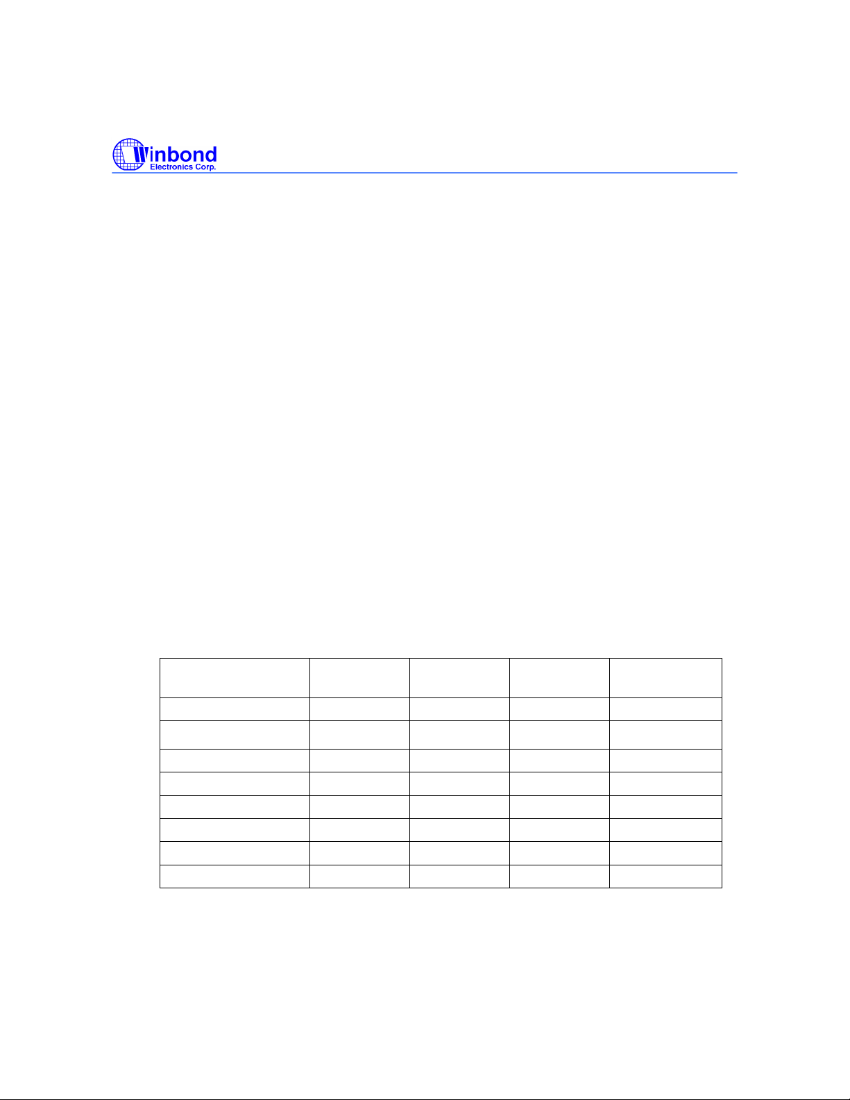
Master Clock Possible Settings
HSR0 (D5)
F
MCLK
13.824 MHz 0 0 0 8 kHz
20.48 MHz 0 0 1 11.852 kHz*
27.648 MHz 0 1 0 8 kHz
40.96 MHz 0 1 1 11.852 kHz*
13.824 MHz 1 0 0 32 kHz*
20.48 MHz 1 0 1 44.1 - 48 kHz
27.648 MHz 1 1 0 32 kHz*
40.96 MHz 1 1 1 44.1-48 kHz
*not tested
(CFG2)
CKD2 (D12)
(CFG2)
CKDV (D8)
(CFG2)
F
SCODEC
Publication Release Date: November 30, 2001
-25 Revision A1
 Loading...