


I5216 SERIES
Advanced Information
PRELIMINARY
8 TO 16 MINUTE VOICE RECORD/PLAYBACK SYSTEM WITH
INTEGRATED CODEC
GENERAL DESCRIPTION
The ChipCorder I5216 is an 8 to 16 minute Voice and Data Record and Playback system with
integrated Voice band CODEC. The device works on a single 2.7V to 3.3V supply, and has fully
integrated system functions, including: AGC, microphone preamplifier, speaker driver, memory and
CODEC. The CODEC meets the PCM c onform anc e specif ication of the G.714 recom m endation. Its µLaw and A-law compander meets the specification of the ITU-T G.711 recommendation.
FEATURES
• Single Supply 2.7 to 3.3 Volt operation
• Voice and digital data record and playback system on a single chip
• Industry-leading sound quality
• Low voltage operation
• Message management
• Fully integrated system functions
• Flexible architecture
• Nonvolatile message storage
• Configurable ChipCorder sampling rates of 4 kHz, 5.3kHz, 6.4 kHz and 8kHz
• 8, 10, 12 and 16 minutes duration
• External or internal Voice recorder clock
2
• I
C serial interface (400kHz)
• Configurable analog paths
• 2.2V Microphone Bias Pin
• 100 year message retention (typical)
• 100K analog record cycles (typical)
• 10K digital record cycles (typical)
• Full-duplex (not in I
o External 13.824 MHz, 27.648 MHz, 20.48 MHz or 40.96 MHz master clock
2
o I
S and PCM digital audio interface ports
o Serial transfer data rate from 64 to 3072 Kbps
o Short and Long frame sync formats
o 2s complement and signed magnitude data format
o Complete µ-Law and A-Law companding
o Linear 14 bit ∆Σ PCM CODEC-filter for A/D and D/A converter
o8 kHz or 44.1 kHz – 48 kHz digital audio sampling rate options
o Analog receive and transmit gain adjust
o Configurable setup through the I
2
S mode) single channel speech CODEC with :
2
C interface
Publication Release Date: November 30, 2001
-1 Revision A1

I5216 SERIES
Advanced Information
PRELIMINARY
TABLE OF CONTENTS
GENERAL DESCRIPTION.......................................................................................................1
FEATURES
PIN LAYOUT & DESCRIPTIONS
I5216 BLOCK DIAGRAMS
FUNCTIONAL DESCRIPTION
APPLICATIONS
INTERNAL REGISTERS
MEMORY ORGANIZATION
OPERATION MODES
2
I
C PORT...............................................................................................................................17
2
I
C SLAVE ADDRESS........................................................................................................... 18
2
I
C OPERATION DEFINITIONS............................................................................................19
2
I
C CONTROL REGISTERS.................................................................................................. 21
COMMAND BYTE
FUNCTION BITS
REGISTER BITS
OPCODE SUMMARY
DATABYTES
POWER-UP SEQUENCE
SET MASTER CLOCK DIVISION RATIO
PLAYBACK MODE
RECORD MODE
FEED THROUGH MODE
CALL RECORD
MEMO RECORD
MEMO & CALL PLAYBACK
MESSAGE CUEING
ANALOG MODE
.............................................................................................................................. 1
............................................................................................ 4
....................................................................................................... 6
................................................................................................ 8
SPEECH/SOUND QUALITY
DURATION
FLASH STORAGE
MICROCONTROLLER INTERFACE
PROGRAMMING
.......................................................................................................................... 24
................................................................................................................. 8
...................................................................................................... 9
........................................................................................................ 9
....................................................................................................................... 9
....................................................................................................... 14
.................................................................................................. 17
............................................................................................................ 17
.................................................................................................................. 21
................................................................................................................... 21
.................................................................................................................... 22
............................................................................................................ 22
..................................................................................................... 25
..................................................................................... ......................... 26
...................................................................................................... ............ 26
........................................................................................ ............ 26
....................................................................................................... ............ 30
..................................................................................................... ............ 31
..................................................................................... ............ 32
................................................................................................ ............ 34
...................................................................................................... ............ 34
....................................................................................... 8
.......................................................................... 9
............................................................................. 25
Publication Release Date: November 30, 2001
-2 Revision A1

I5216 SERIES
Advanced Information
PRELIMINARY
AUTO MUTE & AUTO GAIN FUNCTIONS
VOLUME CONTROL DESCRIPTION
SPEAKER & AUX OUT DESCRIPTION
MICROPHONE INPUTS
DIGITAL MODE
WRITING DATA
READING DATA
ERASING DATA
EXAMPLE COMMAND SEQUENCES
PIN DETAILS
DIGITAL I/O PINS
ANALOG I/O PINS
AUXILIARY OUTPUT
AUXILIARY INPUT
POWER & GROUND PINS
SAMPLE LAYOUT FOR PDIP
ELECTRICAL CHARACTERISTICS
ABSOLUTE MAXIMUM RATINGS FOR PACKAGED PARTS
ABSOLUTE MAXIMUM RATINGS FOR DIE
OPERATING CONDITIONS FOR PACKAGED PARTS
OPERATING CONDITIONS FOR DIE
GENERAL PARAMETERS
TIMING PARAMETERS
ANALOG PARAMETERS
2
C INTERFACE TIMING...................................................................................................... 60
I
CODEC PARAMETERS
TIMING DIAGRAMS
2
I
C SERIAL INTERFACE TECHNICAL INFORMATION...................................................... 69
2
I
S SERIAL INTERFACE TECHNICAL INFORMATION ...................................................... 73
DEVICE PHYSICAL DIMENSIONS
DIE BONDING PHYSICAL LAYOUT
ORDERING INFORMATION
....................................................................................................... ............ 41
.................................................................................................................... 41
................................................................................................................... 41
................................................................................................................... 41
........................................................................................................................ 45
.......................................................................................... ............ 40
.................................................................................................... 45
................................................................................................... 48
.............................................................................................. 49
.................................................................................................. 50
..................................................................................... 51
..................................................................................... 53
................................................................................................... 54
........................................................................................................ 55
..................................................................................................... 57
....................................................................................................... 61
............................................................................................................. 62
...................................................................................... 77
…………………………………………………………................. 82
............................................................. ............ 37
..................................................................... ............ 38
.................................................................. ............ 39
................................................................................. 42
................................................................................. 52
................................ 53
........................................................... 53
......................................... 53
.................................................................... 54
.................................................................................... 80
Publication Release Date: November 30, 2001
-3 Revision A1
NC
NC
NC
NC
ISD5216 Pin Layou t
V
V
SDI
SDI
SDIO
SDIO
RAC
RAC
INT
INT
MCLK
MCLK
V
V
CCD
CCD
V
V
CCD
CCD
SCL
SCL
A1
A1
SDA
SDA
A0
A0
V
V
SSD
SSD
SSD
SSD
SSA
SSA
1
1
2
2
3
3
4
4
5
5
6
6
7
7
8
8
9
9
10
10
11
11
12
12
13
13
14
14
ISD5216
I5216
I5216 SERIES
Advanced Information
PRELIMINARY
28
1
V
V
CCD
CCD
SCL
SCL
A1
A1
SDA
SDA
A0
28
28
27
27
26
26
25
25
24
24
23
23
22
22
21
21
20
20
19
19
18
18
17
17
16
16
15V
15V
WS
WS
SCK
SCK
AUX OUT
AUX OUT
AUX IN
AUX IN
V
V
CCA
CCA
SP+
SP+
V
V
SSA
SSA
SP-
SPACAP
ACAP
MICBS
MICBS
MIC-
MICMIC+
MIC+
V
V
SSA
SSA
A0
V
V
SSD
SSD
V
V
SSD
SSD
V
V
SSA
SSA
MIC+
MIC+
MIC-
MIC-
MICBS
MICBS
ACAP
ACAP
SP-
SP-
SSA
SSA
1
2
2
3
3
4
4
5
5
6
6
7
7
8
8
9
9
10
10
11
11
12
12
13
13
14
14
ISD5216
I5216
V
28
V
CCD
CCD
27
27
MCLK
MCLK
26
26
INT
INT
RAC
RAC
25
25
24
24
SDIO
SDIO
23
23
SDI
SDI
22
22
V
V
SSA
SSA
21
21
WS
WS
20
20
SCK
SCK
19
19
18
18
AUX OUT
AUX OUT
17
17
AUX IN
AUX IN
16
16
V
V
CCA
CCA
15
15
SP+V
SP+V
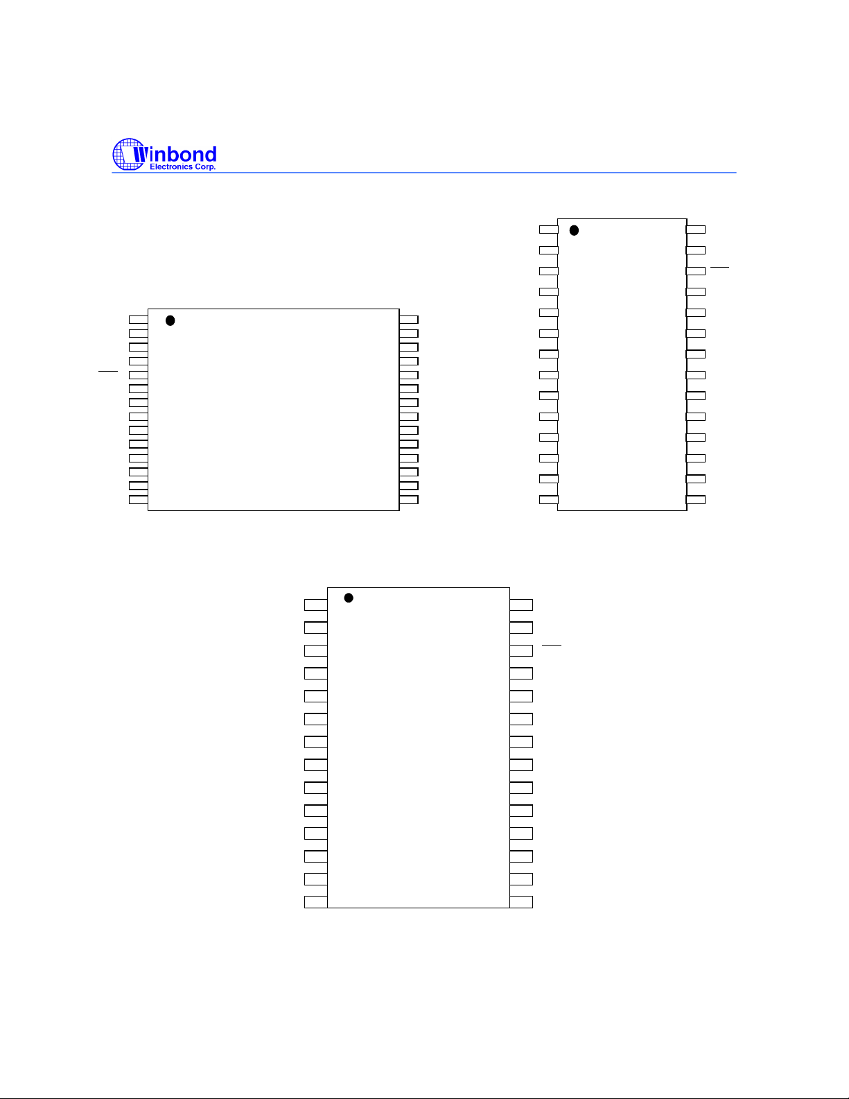
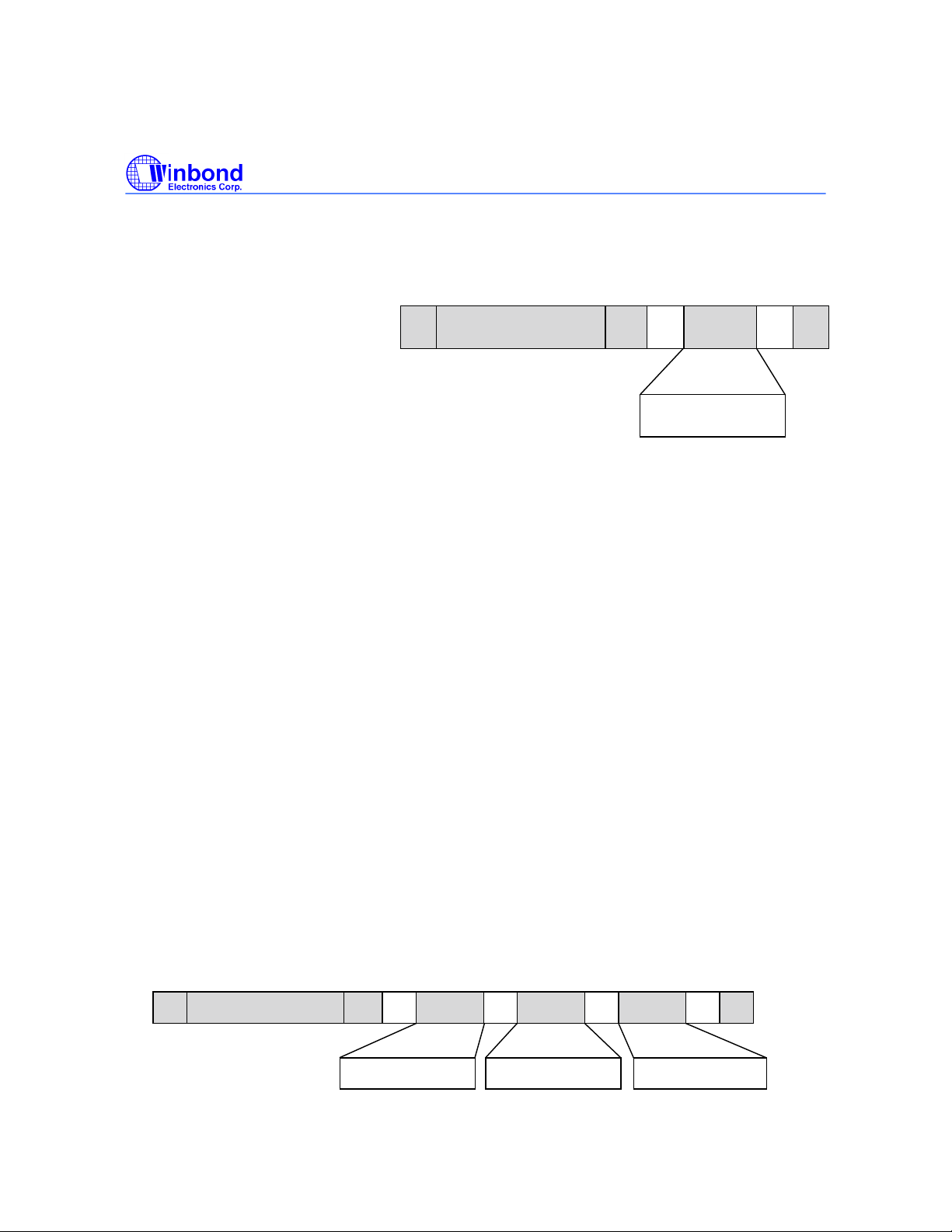
28 -PIN TSOP PDIP/SOIC
28 -PIN TSOP
PDIP
V
CCD
SCL
A1
SDA
V
SSD
V
SSD
A0
MICBS
MICMIC+
V
SSA
ACAP
SP-
V
SSA
1
2
3
4
5
6
7
8
9
10
11
12
13
14
I5216
28
27
26
25
24
23
22
21
20
19
18
17
16
15
V
CCD
MCLK
INT
RAC
SDIO
V
SSA
SDI
NC
AUX OUT
SCK
WS
AUX IN
V
CCA
SP+
SOIC
Publication Release Date: November 30, 2001
-4 Revision A1
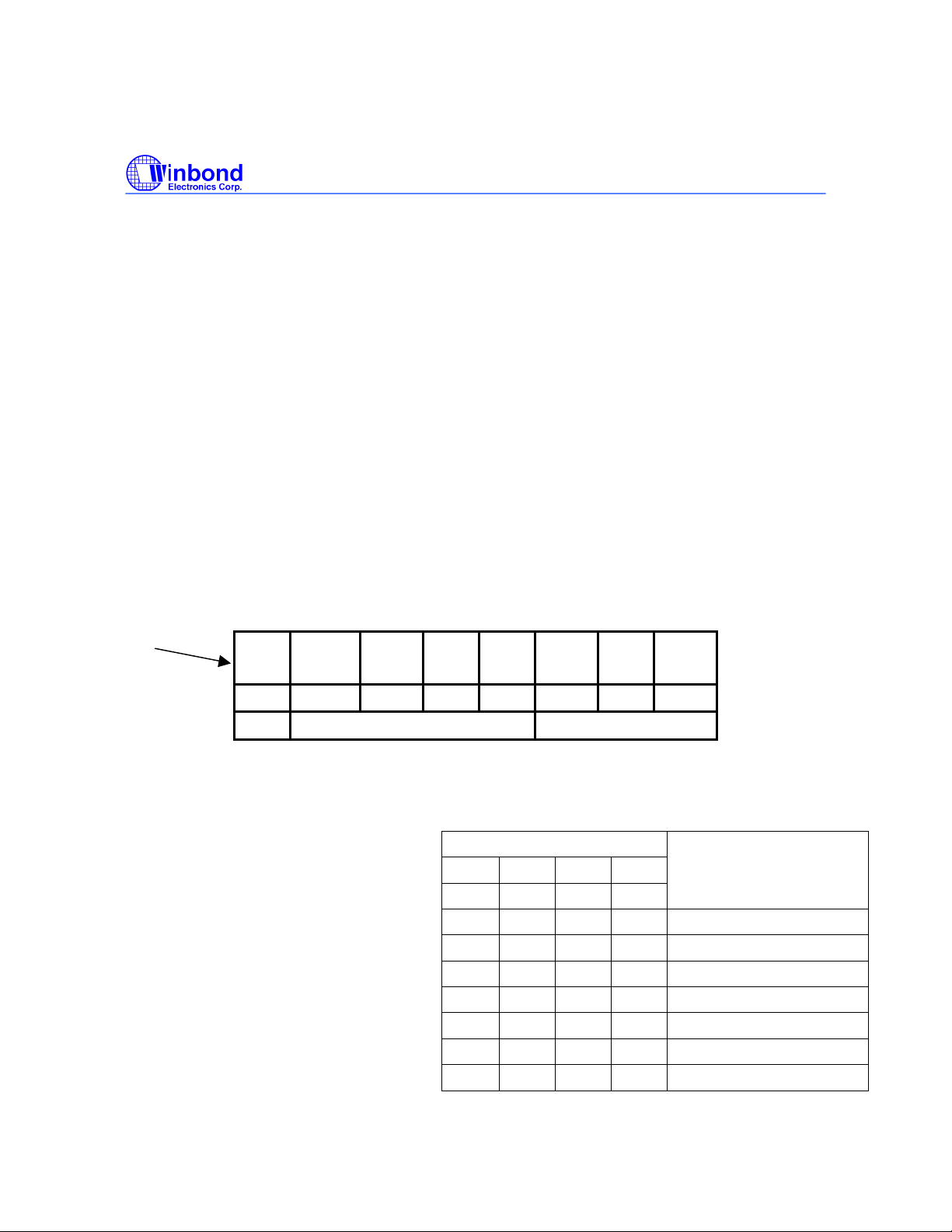
PIN DESCRIPTION
I5216 SERIES
Advanced Information
PRELIMINARY
Pin Name Pin No.
28-pin
TSOP
RAC 4 25 25 Row Address Clock; an open drain output. The RAC pin goes LO W
Pin No.
28-pin
PDIP
Pin No.
28-pin
SOIC
Functionality
1
T
before the end of each row of m emory, and returns HIGH
RACLO
at exactly the end of each row of memory.
/INT 5 26 26 Interrupt Output; an open drain output indicating that a set EOM bit
has been found during Playback, or that the chip is in an Overflow
(OVF) condition. This pin remains LOW until a Read Status
command is executed.
MCLK 6 27 27 This pin allows the internal clock of the Voice record/playback
system to be externally driven for enhanced timing precision. T his
pin is grounded for mos t applications. It is required for the CODEC
operation.
SCL 9 2 2 Serial Clock Line is part of the I2C serial bus. It is used to clock the
data into and out of the I
2
C interface.
SDA 11 4 4 Serial Data Line is part of the I2C serial bus. Data is passed
between devices on the bus over this line.
A0 12 5 7 Input pin that supplies the LSB for the I2C Slave Address.
A1 10 3 3 Input pin that supplies the LSB +1 bit for the I2C Slave Address.
MIC+ 16 9 10 Differential positive Input to the microphone amplifier.
MIC- 17 10 9 Differential negative Input to the microphone amplifier.
MICBS 18 11 8 Microphone Bias Voltage
ACAP 19 12 12 AGC Capacitor connection. Required for the on-chip AGC amplifier.
SP+ 22 15 15 Differential Positive Speaker Driver Output.
SP- 20 13 13 Differential Negative Speaker Driver Output. When the speaker
outputs are in use, the AUX OUT output is disabled.
AUX IN 24 17 17 Auxiliary Input. This is one of the gain adjustable analog inputs for
the device.
AUX OUT 25 18 20 Auxiliary Output. This is one the analog outputs for the device.
When this output is in use, the SP+ and SP- outputs are disabled.
SDI 2 23 22 Serial Digital Audio PCM Input.
SDIO 3 24 24 Serial Digital Audio PCM Output or I2S Input/Output.
WS 28 21 18 Digital audio PCM Frame sync (FS) or I2S Word Sync (WS).
SCK 27 20 19 Digital audio PCM or I2S Serial Clock.
V
7,8 1,28 1,28 Positive Digital Supply pins. These pins carry noise generated by
CCD
internal clocks in the chip. They must be carefully bypassed to
Digital Ground to ensure correct device operation.
V
13,14 6,7 5,6 Digital Ground pins.
SSD
V
1,15,21 8,14,22 11,14,23 Analog Ground pins.
SSA
V
23 16 16 Positive Analog Supply pin. This pin supplies the low level audio
CCA
sections for the device. It should be carefully bypassed to Analog
Ground to ensure correct device operation.
NC 26 19 21 No Connection
1
See parameters section of the datasheet.
Publication Release Date: November 30, 2001
-5 Revision A1
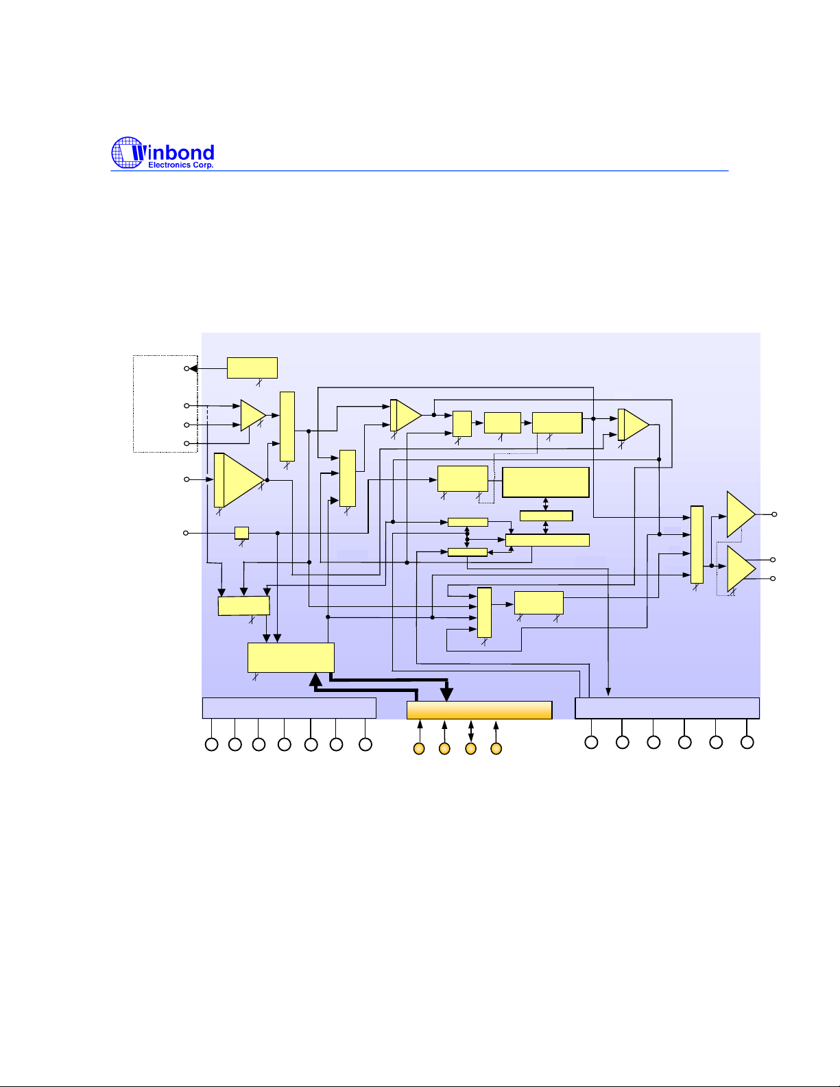
BLOCK DIAGRAMS
I5216 SERIES
Advanced Information
PRELIMINARY
I5216 Block Diagram
MICBS
MICROPHONE
MIC+
MIC -
AGCCAP
AUX IN
MCLK
2.2V Voltage
reference
(AGPD)
AGC
(AGPD)
AUX IN
1.0 / 1.4 / 2.0 / 2.8
AUX IN
AMP
(AXPD)
AXG0
( )
2
AXG1
÷2
(CKD2)
MIC+
1
MIC-
INP
SUM2
C
E
O
D
C
u
x
M
CDI0
2
( )
CDI1
ADPD
2
( )
DAPD
Power Conditioni ng
V
V
CCA
V
SSA
1
Input Source MUX
MIC IN
1
1
(INS0)
1
µµµµ-Law / A-Law /
Linear 14 bit
CODEC
SSAVSSD
V
FILTO
ARRAY
SSD
DAO
SUM1 MUX
S1S0
( )
S1S1
ARRAY OUT
(ANALOG)
V
CCD
SUM1 MUX
( )
2
V
CCD
INP
S1M0
S1M1
SUM1
Summing
AMP
ΣΣΣΣ
SUM1
ARRAY
2
Internal
Clock
OSPD
( )
2
CKDV
( )
SUM2
(ANALOG)
2 x 64 S/H
CTRL
(DIGITAL)
2 x 64-bit reg.
SUM1
DAO
SUM2
PCM / I2S Interface
WS SCK SDIO SDI
MUX
FLD0
FLD1
INP
Filter
(FLS0)
1
Auto mute
Auto gain
1
(AMT0)
Storage Array
2
A/D
Program/Read Control
Vol MUX
VLS0
( )
VLS1
2
Low Pass
Filter
1
Multilevel
Array I/O Mux
Volume
Control
(VLPD)
1
(FLPD)
( )
3
ARRAY OUT
(DIGITAL)
VOL0
VOL1
VOL2
SCL
SUM1
FILTO
AUX IN
SUM2
Summing
AMP
ΣΣΣΣ
S2M0
( )
2
S2M1
FILTO
SUM2
VOL
DAO
Device Control
RACINTSDA
Output MUX
2
OPS0
( )
OPS1
AUX
OUT
AMP
Spkr.
AMP
2
OPA0
( )
OPA1
A1A0
AUX OUT
SPEAKER
SP+
SP-
5/22/01
Publication Release Date: November 30, 2001
-6 Revision A1
I5216 SERIES
(
)
Advanced Information
PRELIMINARY
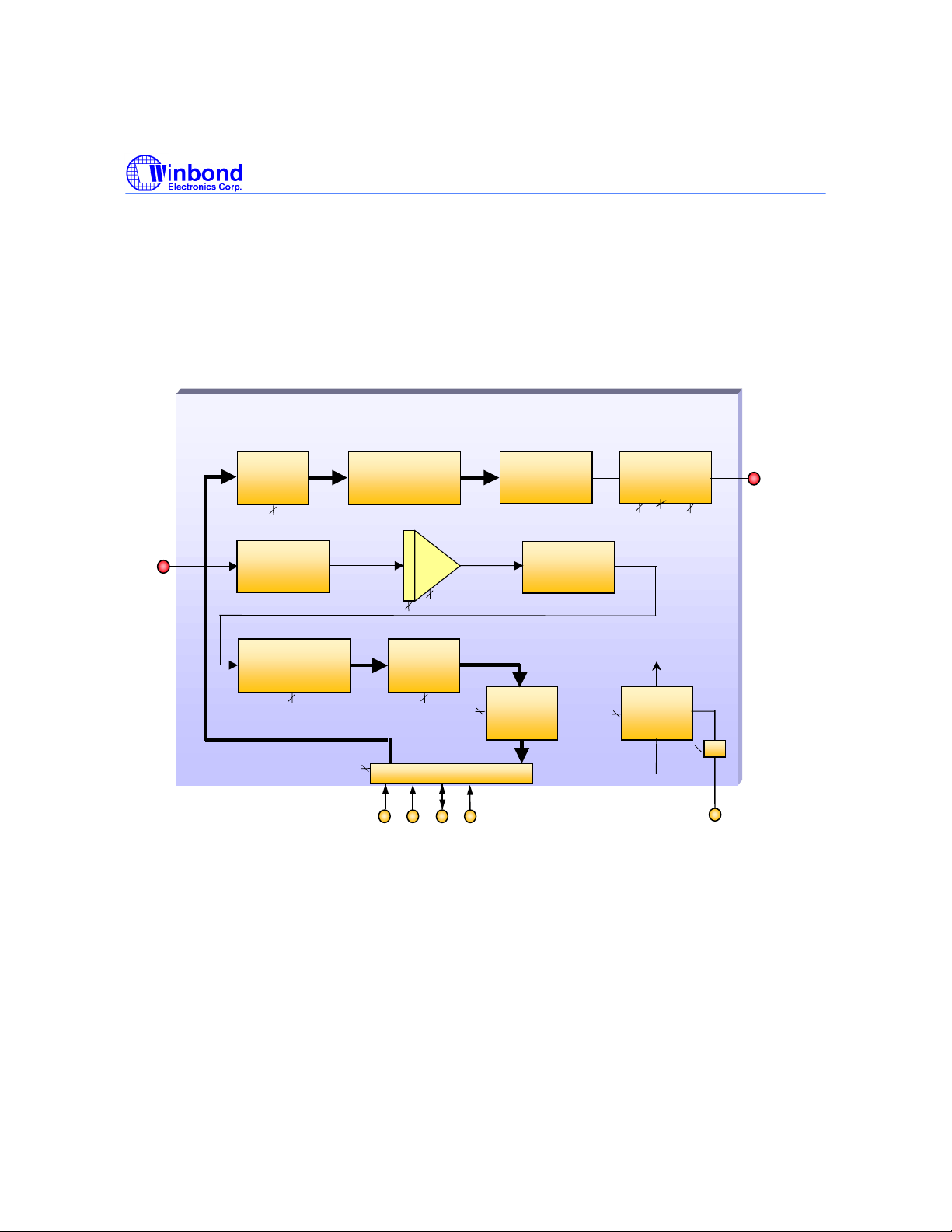
I5216 CODEC DIA G RAM
ANALOG IN
5/8/01
µ/A-Law
Expander
or linear
LAW0
2
LAW1
( )
Anti
Aliasing
Filter
Digital
Anti-Aliasing
Decimation Filter
MUTE
( )
1
1
8 bits or 16
bits
14 bit
Interpolation Filter
CIG0
CIG1
( )
CIG2
15 bit
1
I2S0
( )
Digital
Smoothing
0.8/1/1.2/1.25/1.4/1.6/1.8/2
SC
AMP
(ADPD)
1
3
Digital
High pass
Filter
HPF0
( )
WS SCK SDIO SDI
2
HSR0
( )
PCM / I2S Interface
LAW0
LAW1
14 bit
14 bit
2
Digital
Σ∆
Demodulator
Modulator
µ/A-Law
Compressor
or linear
8 bits or 16
bits
Analog
Σ∆
1 bit
HSR0
( )
MUTE
( )
1 bit D/A
& SC
Filter
1
1
DAPD
1 bit
Sample frequency
Digital
1
PLL
WS
CKD2
( )
3
COG0
COG1
( )
COG2
1
÷2
MCLK
DAO
ANALOG OUT
Publication Release Date: November 30, 2001
-7 Revision A1

I5216 SERIES
Advanced Information
PRELIMINARY
FUNCTIONAL DESCRIPTION
The I5216 ChipCorder Product provides high quality, fully integrated, single-chip Record/Playback
solutions for 8- to 16-m inute messaging applications that are ideal for use in PBX systems, cellular
phones, automotive communications, GPS/navigation systems, and other portable products. The I5216
product is an enhancement to the ISD5116 arc hitecture, providing: 1) A f ull duplex Voice CODEC with
µ-Law and A-Law compander, with I
reduced noise coupling. This supply can also be used to power down the external m icrophone with the
system.
Analog functions and audio gating have also been integrated into the I5216 product to allow for easy
interfacing with integrated chip sets on the market. Audio paths have been designed to enable full
duplex conversation record, voice memo and answering machine (including outgoing message
playback).
Logic Interface Options of 2.0V and 3.0V ar e supported by the I5216 to accomm odate both portable
communication (2.0- and 3.0-volt required) and automotive product customers (5.0-volt required).
Like other ChipCorder
filters, and multi-level storage array on a single chip. For enhanced voice features, the I5216 eliminates
external circuitry by integrating automatic gain control (AGC), a power am plif ier/speak er driver, volum e
control, summing am plifiers, analog switches, and a Voice CODEC. Input level adjustable am plifiers
are also included, providing a flexible interface for multiple applications.
Recordings are stored in on-chip nonvolatile m emory cells, providing zero-power message storage.
This unique, single-chip solution is made possible through Winbond’s patented multilevel storage
technology. Voice and audio signals are stored directly into solid-state memory in their natural,
uncompressed form, providing superior quality voice and music reproduction.
products, the I5216 integrates the sam pling clock, anti-aliasing and sm oothing
2
S and PCM interface ports; 2) A 2.2V m icrophone bias supply for
SPEECH/SOUND QUALITY
The I5216 ChipCorder product can be configured, via software, to operate at 4.0, 5.3, 6.4, and 8.0 kHz
sampling frequencies, allowing the user a choice of speech quality options. Increasing the duration
decreases the sampling frequency and bandwidth, which affects sound quality. The "Input Sample
Duration" table below compares filter pass band and product durations.
DURATION
To meet end-system r equirements, the I5216 device is a single-c hip solution, which provides 8 to 16
minutes of voice record and playback, depending on the sample rates defined by the customer's
software.
INPUT SAMPLE RATE TO DURATION INPUT SAMPLE
Rate (kHz) Duration
(Minutes)
8.0 8 min 3 sec 3.7
6.4 10 min 4 sec 2.9
5.3 12 min 9 sec 2.5
4.0 16 min 6 sec 1.8
1. Minus any pages selected for digital storage
1
Typical Filter Pass Band (kHz)
Publication Release Date: November 30, 2001
-8 Revision A1

I5216 SERIES
Advanced Information
PRELIMINARY
FLASH STORAGE
One of the benefits of W inbond’s ChipCorder technology is the use of on-chip nonvolatile memory,
which provides zero-power message storage. A message is retained for up to 100 years (typically)
without power. In addition, the device can be re-recorded over 10,000 times (typically) for digital
messages and over 100,000 times (typically) for analog messages.
A new feature has been added that allows for the allocation of m emory space in the I5216, to either
digital or analog storage, when recording. When m ak ing a recording, if a section is assigned for digital
or analog data storage, the system microcontroller stores this information in the Message Address
Table.
MICROCONTROLLER INTERFACE
The I5216 is controlled through an I2C 2-wire interface. This synchronous serial port allows commands,
configurations, address data, and digital data to be loaded to the device, while allowing status, digital
data and current address information to be read back from the device. In addition to the serial
interface, two other pins can be connected to the microcontroller for enhanced interface: the RAC
timing pin and the INT\ pin for interrupts to the controller. Communications with all of the internal
registers is through the serial bus, as well as digital memory Read and Write operations.
PROGRAMMING
The I5216 series is also ideal for playback-only applications, whereas single or m ultiple messages may
be played back when desired. Playback is controlled through the I
configuration is created, duplicates can easily be generated via a W inbond or third-party program mer.
For more inform ation on available application tools and programmers , please see the Winbond web
site at http://www.winbond-usa.com/
.
2
C port. Once the desired m essage
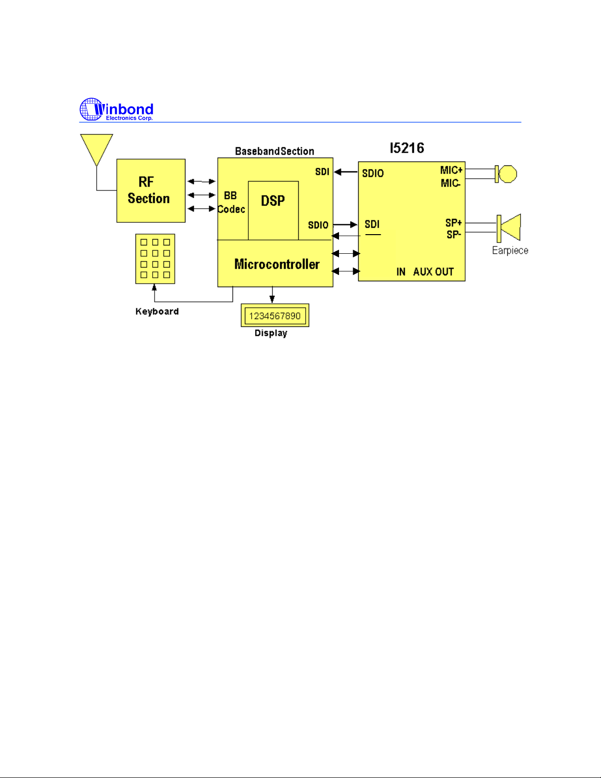
APPLICATIONS
The I5216 is a single chip solution for voice and analog storage that also includes the capability to
store digital information in the m emory array. T he array may be divided between analog and digital
storage, as the user chooses, when configuring the device.
Looking at the block diagram on the following page, one can see that the I5216 may be very easily
designed into a cellular phone. Placing the device between the microphone and the exis ting baseband
chip takes care of the transmit path. The SDI/SDIO of the baseband chip is connected to the SDIO/SDI
of the I5216. Two pins are needed for the I
2
C digital control and digital information for storage.
Publication Release Date: November 30, 2001
-9 Revision A1
I5216 SERIES
Advanced Information
PRELIMINARY
INT
SCL
SDA
Starting at the MICROPHONE inputs, the input signal at the MICROPHONE inputs c an be routed in
the following ways:
• directly through the Voice band CODEC of the I5216 chip, then through the SDIO pin, to output
the digital PCM signal.
• through the AGC amplifier, before it is routed to the voice band CODEC.
• through the AGC amplifier to the storage array
• through the AGC amplifier and mixed with an analog voice band CODEC signal c oming from
the digital SDI pin
In addition, if the phone is inserted into a "hands-free" car kit, then the signal from the pickup
microphone in the car can be passed through to the s ame places from the AUX IN pin and the phone's
microphone is switched off. In this s cenario, the other party's voice from the phone would be played
into the PCM IN input and passed through to the AUX OUT pin that would drive the car kit's
loudspeaker.
Depending upon whether one desires recording one side (simplex) or both sides (duplex) of a
conversation, the various paths will also be switched through to the low pass filter (for antialiasing) and
into the storage array. Later, the cell phone owner can play back the messages from the array. When
this happens, the Array Output MUX is connected to the volume control, through the Output MUX, to
the Speaker Amplifier. For applications other than a cell phone, the audio paths can be s witched into
many different and flexible configurations. Some examples follow.
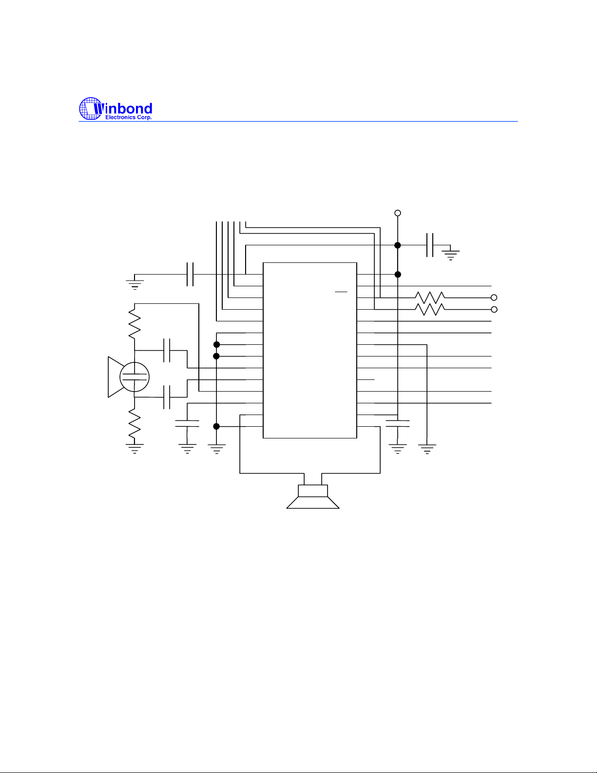
Publication Release Date: November 30, 2001
-10 Revision A1

A
A
A
A
5
µ
A
Electret Microphone
WM-54B Panasonic
1.5kΩ
1.5kΩ
.1
.1µF
.1µF
F
To Microcontroller
2
C interface and
I
ddress setting
1µF
TRANSFORMER APPLICATION
V
3
4
5
6
7
8
9
10
12
14
600Ω
CCD
SCL
1
SDA
0
V
SSD
V
SSD
V
SSA
MIC+
MICMICBS
CAP
SPV
SSA
600Ω
AUX OUT
=
=
V
CCD
MCLK
INT
RAC
SDIO
SDI
V
SSA
WS
SCK
NC
AUX IN
V
CC
SP+
27
26
25
24
23
22
21
20
19
18
17
1
I5216 SERIES
Advanced Information
PRELIMINARY
Vcc
.1µF
4.7KΩ
.1µF
Vcc
Vcc
PCM OUT
PCM IN
8 KHz
2.048 MHz
.1µF
Publication Release Date: November 30, 2001
-11 Revision A1
I5216 SERIES
A
A
A
9
µ
A
g
Advanced Information
PRELIMINARY
Electret Microphone
WM-54B Panasonic
HANDSET APPLICATION
.1µF
1.5kΩ
.1µF
F
.1
1.5kΩ
To Microcontroller
I
.1µF
2
C interface and
ddress settin
1
2
3
4
5
6
7
8
9
10
11
12
13
14
V
CCD
SCL
1
SDA
0
V
SSD
V
SSD
V
SSA
MIC+
MICMICBS
CAP
SP
V
SSA
Vcc
.1µF
AUX OUT
AUX IN
V
CCD
MCLK
RAC
SDIO
SDI
V
SSA
SCK
NC
V
CCA
SP+
28
27
26
25
24
23
22
21
1
18
17
16
15
.1µF
4.7KΩ
4.7KΩ
13.824 MHz
Vcc
Vcc
PCM OUT
PCM IN
8 KHz
2.048 MHz
TO RINGER
Publication Release Date: November 30, 2001
-12 Revision A1
A
A
A
318
A
g
S S
/O
3.0
ccVccVcc
Electret Microphone
WM-54B Panasonic
1.5kΩ
1.5kΩ
.1µF
.1µF
.1µF
1µF
CAR STEREO APPLICATION
To Microcontroller
2
C interface and
I
ddress settin
1
V
2
3
4
5
7
8
10
11
12
13
14
CCD
SCL
1
SDA
0
6
V
SSD
V
SSD
V
SSA
9
MIC+
MICMICBS
CAP
SP-
SSA
V
CCD
MCLK
INT
RAC
SDIO
SDI
V
SSA
WS
SCK
NC
AUX OUT
AUX IN
V
CCA
SP+V
I5216 SERIES
Advanced Information
PRELIMINARY
V
.1µF
4.7KΩ
4.7KΩ
24
2
17
.1µF
20.48 MHz
2
I
ERIAL I
48 KHz
72 MHz
Publication Release Date: November 30, 2001
-13 Revision A1
I5216 SERIES
Advanced Information
PRELIMINARY
INTERNAL REGISTERS
The following tables provide a general illustration of the bits. T here are three configuration registers:
CFG0, CFG1 and CFG2. Thus, there are six 8-bit bytes to be loaded during the set-up of the device.
CFG0
Bit no. Signal Description
D0 (LSB) VLPD Power down the Volume Control.
D1 OPA0 Power down Speaker driver and/or Auxiliary output.
D2 OPA1 Power down Speaker driver and/or Auxiliary output.
D3 OPS0 Select speaker output multiplexer.
D4 OPS1 Select speaker output multiplexer.
D5 CDI0 Analog to digital converter input selector.
D6 CDI1 Analog to digital converter input selector.
D7 AMT0 Compress the filter signal.
D8 OSPD Power down the internal ChipCorder oscillator.
D9 INS0 Select Microphone input or Auxiliary input.
D10 AXPD Power down Auxiliary input amplifier.
D11 AXG0 Auxiliary input amplifier gain setting.
D12 AXG1 Auxiliary input amplifier gain setting.
D13 CIG0 Input gain setting for the Analog to digital converter.
D14 CIG1 Input gain setting for the Analog to digital converter.
D15 (MSB) CIG2 Input gain setting for the Analog to digital converter.
Publication Release Date: November 30, 2001
-14 Revision A1
PRELIMINARY
CFG1
Bit no. Signal Description
D0 (LSB) AGPD Power down the Microphone AGC
D1 FLPD Power down the Filter
D2 FLD0 Set the duration and sample rate of the ChipCorder
D3 FLD1 Set the duration and sample rate of the ChipCorder
D4 FLS0 Select the filter input signal
D5 S2M0 Select Sum Amplifier 2 input
D6 S2M1 Select Sum Amplifier 2 input
D7 S1M0 Select Sum Amplifier 1 input
D8 S1M1 Select Sum Amplifier 1 input
D9 S1S0 Select Sum Amplifier 1 multiplexer
D10 S1S1 Select Sum Amplifier 1 multiplexer
D11 VOL0 Volume Control Setting
D12 VOL1 Volume Control Setting
D13 VOL2 Volume Control Setting
D14 VLS0 Select Volume Control input
D15 (MSB) VLS1 Select Volume Control input
I5216 SERIES
Advanced Information
Publication Release Date: November 30, 2001
-15 Revision A1

I5216 SERIES
Advanced Information
PRELIMINARY
CFG2
Bit no. Signal Description
D0 (LSB) ADPD Power down the Analog to Digital converter
D1 DAPD Power down the Digital to Analog converter
D2 LAW0
D3 LAW1
D4 I2S0 Select the I2S interface
D5 HSR0 Enable the high sample rate mode
D6 HPF0 Enable High Pass Filter
D7 MUTE Mute the CODEC A/D and D/A path
D8 CKDV Divide MCLK by 2560 or 1728 for 8 kHz ChipCorder sample rate
D9 COG0 Output gain setting for the Digital to Analog converter
D10 COG1 Output gain setting for the Digital to Analog converter
D11 COG2 Output gain setting for the Digital to Analog converter
D12 CKD2 Divide MCLK frequency by 2 or 1
D13 - Reserved
D14 - Reserved
D15 (MSB) - Reserved
Select digital µ-Law or A-Law input/output format
Select digital µ-Law or A-Law input/output format
Publication Release Date: November 30, 2001
-16 Revision A1

I5216 SERIES
Advanced Information
PRELIMINARY
MEMORY ORGANIZATION
The I5216 memory array is arranged as 1888 rows (or pages) of 2048 bits, for a total memory of
3,866,624 bits. The primary addressing for the 2048 pages is handled by 11 bits of address data in the
analog mode. At the 8 kHz sample r ate, each page contains 256 m illisec onds of audio. T hus , at 8 k Hz
there is actually room for 8 minutes and 3 seconds of audio.
A memory page is 2048 bits organized as thirty-two 64-bit "blocks " when used f or digital s tor age. The
contents of a page are either analog or digital. T his is determined by instruction (op code) at the time
the data is written. A record of what is analog and what is digital, and where, is stored by the system
microcontroller in the m essage address table (MAT). The MAT is a table kept in the microcontroller
memory that defines the status of each message “block.” It can be s tored back into the I5216 if the
power fails or the system is turned of f. Use of this table allows for efficient message managem ent.
Segments of messages can be stored wherever there is available space in the m emory array. [This
is explained in detail for the Winbond I5008 in Applications Note #No.9 and will similar ly be in a later
Note for the I5216.]
When a page is used for analog stor age, the same 32 block s are pres ent, but there are 8 EOM (Endof-Message) m arkers. This means that for each 4 blocks there is an EOM marker at the end. Thus,
when recording, the analog recording will stop at any one of eight positions. At 8 kHz, this results in a
resolution of 32 msec when ENDING an analog recording. Beginning an analog recor ding is limited to
the 256 msec resolution provided by the 11-bit address. A recording does not imm ediately stop when
the Stop command is issued, but continues until the 32-m illisecond block is filled. T hen a bit is placed
into the EOM memory to develop the interrupt that signals a message is finished playing in the
Playback mode.
2
Digital data is sent and received, serially, over the I
and stored in one of two alternating (commutating) 64- bit shift register s. W hen an input register is full,
it becomes the register that is par allel written into the array. The prior write register becom es the new
serial input register. A mechanis m is built in to ensure there is always a register available for s toring
new data.
Storing data in the memory is accomplished by accepting data, one byte at a time, and issuing an
acknowledgement. If data is coming in faster than it can be written, then the chip will not issue an
acknowledgement to the host microcontroller until it is ready.
The read mode is the opposite of the write m ode. Data is r ead into one of two 64-bit regis ters f rom the
array and serially sent to the I
2
C port. (See Digital Mode on page 41 for details).
C interface. The data is ser ial-to-parallel c onverted
OPERATION MODES DESCRIPTION
I2C PORT
Important note: The content contained herein of the r est of t his datasheet assum es t hat the
reader is familiar with the I
2
C section of this document. If you are not familiar with this serial prot ocol, please read
the I
the I2C section to familiarize yourself with it. A significant amount of additional information on
2
C can also be found on the Philips web page at http://www.philips.com/.
I
2
C serial interface. Additional informat ion on I2C may be found in
Publication Release Date: November 30, 2001
-17 Revision A1

I5216 SERIES
Advanced Information
PRELIMINARY
I2C SLAVE ADDRESS
The I5216 has a 7 bit slave address of <100 00xy> where x and y are equal to the state, respectively,
of the external address pins A1 and A0. Because all data bytes are required to be 8 bits, the LSB of the
address byte is the Read/Write selection bit that tells the slave whether to transmit or receive data.
Therefore, there are eight possible slave addresses for the I5216
A1 A0 Slave Address R/W\
Bit
0 0 <100 00 00> 0 80
0 1 <100 00 01> 0 82
1 0 <100 00 10> 0 84
1 1 <100 00 11> 0 86
0 0 <100 00 00> 1 81
0 1 <100 00 01> 1 83
1 0 <100 00 10> 1 85
1 1 <100 00 11> 1 87
To use more than four I5216 devices in an application requires some external switching of the I
HEX Value
2
C link.
Publication Release Date: November 30, 2001
-18 Revision A1
I5216 SERIES
e
A
A
A
R
A
A
A
Advanced Information
PRELIMINARY
I2C OPERATION DEFINTIONS
There are many control functions used to operate the I5216. Among them are the following.
READ STATUS COMMAND: The read status command is a read
request from the Host processor to the I5216 without delivering a
Command Byte. The Host supplies all of the clocks (SCL). In each
case, the entity sending the data drives the data line (SDA). The Read
Status Command is executed by the following I
1. Host executes I
2. Send Slave Address with R/W bit = “1” (Read) 81h.
3. Slave responds back to Host an Acknowledge (ACK), followed
by 8 bit Status word.
4. Host sends an Acknowledge (ACK) to Slave.
5. Wait for SCL to go HIGH.
6. Slave responds with Upper Address byte of internal address
register.
7. Host sends an ACK to Slave.
8. Wait for SCL to go high.
9.
Slave responds with Lower Address byte of internal address
register.
10.
Host sends a NO ACK to Slave, then executes I2C STOP
Note: The processor could have sent an I2C STOP after the Status
Word data transfer, and thus aborted the transfer of the Address bytes
A graphical representation of this operation is found below. See the caption box above for more
explanation.
S SLAVE ADDRESS
2
C START
DAT
2
C sequence.
DAT
Conventions used in I2C Data
Transfer Diagrams
S
= START Condition
P
= STOP Condition
DATA
= 8 bit data transfer
R
= “1” in the R/W bit
W
= “0” in the R/W bit
A
= ACK (Acknowledge)
N
= No ACK
SLAVE ADDRESS
The Box color indicates the
direction of data flow
= Host to Slave (Gray)
= Slave to Host (White)
DAT
P
N
= 7 bit Slav
Address
Status
-19 Revision A1
High Addr.
Publication Release Date: November 30, 2001
Low Addr.
I5216 SERIES
A
A
A
A
A
A
Advanced Information
PRELIMINARY
LOAD COMMAND BYTE REGISTER (Single Byte Load)
A single byte may be written to the Command Byte Register in order to power up the device, start or
stop Analog Record (if no address inform ation is needed), or perf orm a Mes sage Cueing f unction. T he
Command Byte Register is loaded as follows:
1. Host executes I2C START.
2. Send Slave Address with R/W bit = “0” (Write) [80h].
3. Slave responds back with an ACK.
4. Wait for SCL to go HIGH.
5. Host sends a command byte to Slave.
6. Slave responds with an ACK.
7. Wait for SCL to go HIGH.
8. Host executes I
2
C STOP.
S SLAVE ADDRESS A DATA
W
Command Byte
A
LOAD COMMAND BYTE REGISTER (Address Load):
For the normal addressed mode the Registers are loaded as follows:
2
1. Host executes I
2. Send Slave Address with R/W bit = “0” (Write).
3. Slave responds back with an ACK.
4. Wait for SCL to go HIGH.
5. Host sends a byte to Slave - (Command Byte).
6. Slave responds with an ACK.
7. Wait for SCL to go HIGH.
8. Host sends a byte to Slave - (High Address Byte).
9. Slave responds with an ACK.
10. Wait for SCL to go HIGH.
11. Host sends a byte to Slave - (Low Address Byte).
12. Slave responds with an ACK.
13. Wait for SCL to go HIGH.
14. Host executes I
S SLAVE ADDRESS
C START.
2
C STOP.
Command
DAT
DAT
High Addr. Low Addr.
DATA
PW
Publication Release Date: November 30, 2001
-20 Revision A1
I5216 SERIES
Advanced Information
PRELIMINARY
I2C CONTROL REGISTERS
The I5216 is controlled by loading comm ands to, or reading commands fr om the internal command,
configuration and address register s. T he Com m and byte sent is used to star t and stop r ecording, write
or read digital data and perform other functions necessary for the operation of the device.
COMMAND BYTE
Control of the I5216 is implemented through an 8-bit com mand byte that is sent after the 7-bit device
address and the 1-bit Read/Write selection bit. The 8 bits are:
Global power up bit
DAB bit: determines whether device is performing an analog or digital function
3 func tion bits: these determ ine which function the device is to perf orm in conjunction with the
DAB bit.
3 register address bits: these determine if and when data is to be loaded to a register
Power Up Bit
C7
PU DAB FN2 FN1 FN0 RG2 RG1 RG0
Function Bits Register Bits
C6 C5 C4 C3 C2 C1 C0
FUNCTION BITS
The command byte function bits are detailed
in the table to the right. C6, the DAB bit,
determines whether the device is
performing an analog or digital f unc tion. T he
other bits are decoded to produce the
individual commands. Note that not all
decode combinations are currently used;
they are reserved for future use. Out of 16
possible codes, the I5216 uses 7 f or norm al
operation. The other 9 are No Ops.
-21 Revision A1
Command Bits
C6 C5 C4 C3
DAB FN2 FN1 FN0
0 0 0 0 STOP (or do nothing)
0 1 0 1 Analog Play
0 0 1 0 Analog Record
0 1 1 1 Analog MC
1 1 0 0 Digital Read
1 0 0 1 Digital Write
1 0 1 0 Erase (row)
Publication Release Date: November 30, 2001
Function
I5216 SERIES
Advanced Information
PRELIMINARY
REGISTER BITS
The register load may be used to modify
a command sequence (such as load an
address) or used with the null command
sequence to load a configuration or test
register. Not all registers are accessible to
the user. [The remaining three codes are
No Ops.]
RG2 RG1 RG0
C2 C1 C0
0 0 0 No action
0 0 1 Load Address
0 1 0 Load CFG0
0 1 1 Load CFG1
1 0 1 Load CFG2
Function
OPCODE SUMMARY
OpCode Command Description
The following commands are used to access the chip through the I2C port:
Play: analog play command.
Record: analog record command.
Message Cue: analog message cue command.
Enter Digital mode.
Read: digital read command.
Write: digital write command.
Erase: digital page and block erase command.
Exit Digital mode.
Power up: global power up/down bit. (C7).
Load address: load address register (is incorporated in play, record, read and write
commands).
Load CFG0: load configuration register 0.
Load CFG1: load configuration register 1.
Load CFG2: load configuration register 2.
Read STAT US: Read the interrupt status and address register , including a hardwired device
ID.
Publication Release Date: November 30, 2001
-22 Revision A1
I5216 SERIES
Advanced Information
PRELIMINARY
OPCODE COMMAND BYTE TABLE
Pwr Function Bits Register Bits
OPCODE HEX PU DAB FN2 FN1 FN0 RG2 RG1 RG0
COMMAND BIT NUMBER CMD C7 C6 C5 C4 C3 C2 C1 C0
POWER UP 80 1 0 0 0 0 0 0 0
POWER DOWN 00 0 0 0 0 0 0 0 0
STOP (DO NOTHING) STAY ON 80 1 0 0 0 0 0 0 0
STOP (DO NOTHING) STAY OFF 00 0 0 0 0 0 0 0 0
LOAD ADDRESS 81 1 0 0 0 0 0 0 1
LOAD CFG0 82 1 0 0 0 0 0 1 0
LOAD CFG1 83 1 0 0 0 0 0 1 1
LOAD CFG2 85 1 0 0 0 0 1 0 1
RECORD ANALOG 90 1 0 0 1 0 0 0 0
RECORD ANALOG @ ADDR 91 1 0 0 1 0 0 0 1
PLAY ANALOG A8 1 0 1 0 1 0 0 0
PLAY ANALOG @ ADDR A9 1 0 1 0 1 0 0 1
MSG CUE ANALOG B8 1 0 1 1 1 0 0 0
MSG CUE ANALOG @ ADDR B9 1 0 1 1 1 0 0 1
ENTER DIGITAL MODE C0 1 1 0 0 0 0 0 0
ERASE DIGITAL PAGE D1 1 1 0 1 0 0 0 1
WRITE DIGITAL C8 1 1 0 0 1 0 0 0
WRITE DIGITAL @ ADDR C9 1 1 0 0 1 0 0 1
READ DIGITAL E0 1 1 1 0 0 0 0 0
READ DIGITAL @ ADDR E1 1 1 1 0 0 0 0 1
EXIT DIGITAL MODE 40 0 1 0 0 0 0 0 0
READ STATUS REGISTER
1
N/A N/A N/A N/A N/A N/A N/A N/A N/A
Publication Release Date: November 30, 2001
-23 Revision A1
I5216 SERIES
Advanced Information
PRELIMINARY
1
See Playback and Stop Cycle on page 62 for details.
DATABYTES
In the I2C write mode, the device can accept data sent after the command byte. If a register load option
is selected, the next two bytes are loaded into the selected register. The format of the data is MSB first,
as specified by the I
the byte is acknowledged, and DATA<7:0> is sent next. The address regis ter consists of two bytes.
The format of the address is as follows:
ADDRESS<15:0> = PAGE_ADDRESS<10:0>, BLOCK_ADDRESS<4:0>
If an analog function is selected, the bloc k addr ess bits m ust be s et to 00000. Digital Read and Write
are block addressable.
When the device is polled with the Read Status command, it will return three bytes of data. T he first
byte is the status byte, the next is the upper address byte and the last is the lower address byte. The
status register is one byte long and its bit function is:
STATUS<7:0> = EOM, OVF, READY, PD, PRB, DEVICE_ID<2:0>
The lower address byte will always return the block address bits as zero, either in digital or analog
mode.
The functions of the bits are:
2
C standard. Thus to load DATA<15:0> into the devic e, DATA<15:8> is sent fir st,
BIT# NAME FUNCTION
7 EOM Indicates whether an EOM interrupt has occurred.
6 OVF Indicates whether an overflow interrupt has occurred.
5 READY Indicates the internal status of the device – if READY is LOW no new
commands should be sent to device.
4 PD Device is powered down if PD is HIGH.
3 PRB Play/Record mode indicator. HIGH=Play/LOW=Record.
2
1
DEVICE_ID
0
It is good practice to read the status register after a Write or Record operation to ensure that the
device is ready to accept new commands. Depending upon the design and the number of pins
available on the controller, the polling overhead can be reduced. If INT\ and RAC are tied to the
microcontroller, the controller does not have to poll as frequently to determine the status of the I5216
An internal device ID. This is 001 for the I5216.
Publication Release Date: November 30, 2001
-24 Revision A1
I5216 SERIES
Advanced Information
PRELIMINARY
POWER-UP SEQUENCE
This sequence prepares the I5216 for an operation to follow, and waits for the Tpud time before
sending the next command sequence.
2
1. Send I
2. Send one byte 10000000 {Slave Address, R/W = 0} 80h.
3. Slave ACK.
4. Wait for SCL High.
5. Send one byte 10000000 {Command Byte = Power Up} 80h.
6. Slave ACK.
7. Wait for SCL High.
8. Send I
C Start.
2
C Stop.
SET MASTER CLOCK DIVISION RATIO
The I5216 product has two Master Clock configuration bits that allow four possible Master Clock
frequencies. The Master Clock Division ratios can be set by bits CKD2 and CKDV. Thes e are bits D12
and D8 of CFG2, respectively. The combination of these bits, with the sample rate bit HSR0, also sets
the CODEC sample frequency.
Master Clock Possible Settings
HSR0 (D5)
F
MCLK
13.824 MHz 0 0 0 8 kHz
20.48 MHz 0 0 1 11.852 kHz*
27.648 MHz 0 1 0 8 kHz
40.96 MHz 0 1 1 11.852 kHz*
13.824 MHz 1 0 0 32 kHz*
20.48 MHz 1 0 1 44.1 - 48 kHz
27.648 MHz 1 1 0 32 kHz*
40.96 MHz 1 1 1 44.1-48 kHz
*not tested
(CFG2)
CKD2 (D12)
(CFG2)
CKDV (D8)
(CFG2)
F
SCODEC
Publication Release Date: November 30, 2001
-25 Revision A1

SDI
SDISDI
WS
WSWS
SCK
SCKSCK
SDIO
SDIOSDIO
I5216 SERIES
Advanced Information
PRELIMINARY
PLAYBACK MODE
The command sequence for an analog Playback operation can be handled several ways. One
technique is to do a Load Address (81h), which requires sending a total of four bytes, followed by a
Play Analog, which is a Command Byte (A8h) preceded by the Slave Address Byte. This is a total of six
bytes plus the times for Start, ACK, and Stop.
Another approach for an analog Playback operation is via a single four byte exchange, which consists
of the Slave Address (80h), the Command Byte (A9h) for Play Analog @ Address, and the two address
bytes.
RECORD MODE
The command sequence for an Analog Record is a four byte sequence consisting of the Slave
Address (80h), the Command Byte (91h) for Record Analog @ Address, and the two address bytes.
2
(See I
FEED THROUGH MODE
C Interface on page 17 for more detail.)
µ
/A-Law
µ
1
1
1
(I2S0)
(I2S0)
(I2S0)
/A-Law
Expander
Expander
2
2
2
(LAW1,LAW0)
(LAW1,LAW0)
(LAW1,LAW0)
PCM Interface
PCM Interface
µ
/A-Law
µ
/A-Law
Compressor
Compressor
2
2
2
(LAW1,LAW0)
(LAW1,LAW0)
(LAW1,LAW0)
DAC
DAC
3
3
(DAPD,HSR0,MUTE)
(DAPD,HSR0,MUTE)
ADC
ADCADC
4
(ADPD,HSR0,HPF0,MUTE)
(ADPD,HSR0,HPF0,MUTE)
4
Output
Output
GAIN
GAIN
3
3
(COG2,COG1,COG0)
(COG2,COG1,COG0)
Input
Input
GAIN
GAIN
3
3
(CIG2,CIG1,CIG0)
(CIG2,CIG1,CIG0)
FILTO+
FILTO+
VOL+
VOL+
SUM2+
SUM2+
DAO+
DAO+
DAO-
DAOSUM2-
SUM2VOL-
VOL-
FILTO-
FILTO-
Output MUX
Output MUX
2
2
(OPS1,O PS0)
(OPS1,O PS0)
CODEC In Mux
CODEC In Mux
CODEC In Mux
2
2
(CDI1,CDI0)
(CDI1,CDI0)
Spkr.
Spkr.
AMP
AMP
2
2
(OPA1,O PA0)
(OPA1,O PA0)
SUM2+
SUM2+
SUM2+
SUM2+
INP+
INP+
INP+
INP+
INP-
INP-
INP-
INPSUM2-
SUM2-
SUM2-
SUM2-
SPEAKER
SPEAKER
SP+
SP+
SP-
SP-
MIC+
MIC+
MIC+
MIC+
MIC -
MIC -
MIC -
MIC -
This diagram shows the part of the I5216 block diagram that is used in Feed Through Mode. The rest of the chip
will be powered down to conserve power. Note that the Microphone and Speaker +/– paths are differential
Publication Release Date: November 30, 2001
- 26 - Revision A1

I5216 SERIES
Advanced Information
PRELIMINARY
FEED THROUGH MODE
The previous examples were dependent upon the device already being powered up and the various
paths being set through the device for the desired operation. To set up the device for the various paths
requires loading the three 16-bit Configuration Registers with the correct data. For example, in the
Feed Through Mode, the device only needs to be powered up and a few paths selected. This mode
enables the I5216 to connect to a cellular or cordless baseband phone chip set without affecting the
audio source or destination. There are two paths involved: the transmit path and the receive path. The
transmit path connects the W inbond chip’s microphone source through to the digital audio input on the
baseband chip set. The receive path connects the baseband chip set’s digital output through to the
speaker driver on the Winbond chip. This allows the W inbond chip to substitute for Analog to Digital
and Digital to Analog conversion, and incidentally gain access to the audio, both to and from the
baseband chip set.
To setup the environment described above, a series of commands need to be sent to the I5216. First,
the chip needs to be powered up as described in Power-Up Sequence
Configuration Registers need to be filled with the specific data to connect the desired paths. In the
case of the Feed Through Mode, most of the chip can remain powered down. The Feed Through
Mode diagram illustrates the affected paths
To select the Feed Through mode, the following control bits must be configured in the I5216 configuration register
To set up the transmit path:
1. Select the FTHRU path through the CODEC INPUT MUX—Bits CDI1 and CDI0 control the
state of the CODEC INPUT MUX. These are the D6 and D5 bits, respectively, of Configuration
Register 0 (CFG0) and they should be set to ONE and ZERO, respectively, to select the
FTHRU path.
on page 25. Then the
2. Power up the ADC—Bit ADPD controls the power up state of ADC. This is bit D0 of CFG2 and
it should be a ZERO to power up the ADC.
3. Set the CODEC input gain. The input gain setting will depend on the input level at the MIC+/pins and can be set by the CODEC INPUT GAIN Bits CIG2, CIG1 and CIG0. These are the
D15, D14 and D13 bits, respectively, of Configuration Register 0 (CFG0). The input gain can
be set according to the following table. (Table A)
4. Enable the High Pass Filter, if desired, in the low sample rate mode. This can be done by
setting bit HPF0 to ONE. This is bit D6 of CFG2.
5. Select the low or high sample rate mode by setting bit HSR0. This is bit D5 of CFG2. HSR0
needs to be set to ONE for the high sample rate mode.
6. Set the MUTE bit if desired. This bit can be set temporarily to reduce power up ‘pops’ or to set
the system on hold. This bit is D7 of CFG2 and needs to be set to ONE in order to mute the
signal.
7. Set the digital data format through bits LAW1 and LAW0. These are bits D3 and D2 of CFG2,
respectively. The data format can be chosen according to the following table. (Table B).
2
8. Set the interface mode to PCM-interface by setting bit I
duplex mode. This bit is bit D4 of CFG2.
9. Set the Master Clock division ratios as described in Set Master Clock Division Ratio
25.
- 27 Revision A1
S0 to ZERO. This will also enable full
on page
Publication Release Date: November 30, 2001

I5216 SERIES
Advanced Information
PRELIMINARY
Table A Table B
CIG2 CIG1 CIG0 GAIN
0 0 0 0.80
0 0 1 1.00
0 1 0 1.20
0 1 1 1.25
1 0 0 1.40
1 0 1 1.60
1 1 0 1.80
1 1 1 2.00
HSRO Sample Rate Mode HPF0 High Pass Filter
0 Low 0 Bypassed
1 High 1 Enabled
ADPD CODEC ADC DAPD CODEC DAC
0 Power Up 0 Power Up
1 Power Down 1 Power Down
I2S0 CONDITION MUTE CONDITION
0 PCM Interface 0 Power Up
1 I2S Interface 1 Mute CODEC ADC & DAC
Table C Table D
Table E Table F
Table G Table H
LAW
1
0 0 Two’s complement
0 1 A-Law
1 0
1 1
LAW
0
Data format
µ-Law
Publication Release Date: November 30, 2001
- 28 Revision A1

I5216 SERIES
Advanced Information
PRELIMINARY
To set up the receive path:
Set up the CODEC output gain amplifier for the correct gain—Bits COG0, COG1 and COG2 control the
gain settings of this amplifier. These are bits D9, D10 and D11, respectively, of CFG2. The table below
will help determine the setting
COG2 COG1 COG0 GAIN (dB)
0 0 0 0
0 0 1 +2
0 1 0 +4
0 1 1 +6
1 0 0 -8
1 0 1 -6
1 1 0 -4
1 1 1 -2
1. Power up the DAC—Bit DAPD controls the power up state of the DAC. This is bit D1 of CFG2
and should be a ZERO to power up the DAC.
2. Select the DAC path through the OUTPUT MUX—Bits OPS0 and OPS1 control the state of
the OUTPUT MUX. These are bits D3 and D4, respectively, of CFG0 and they should be set to
the state where D3 is ONE and D4 is ZERO to select the DAC path.
3. Power up the Speaker Amplifier—Bits OPA0 and OPA1 control the state of the Speaker and
AUX amplifiers. These are bits D1 and D2, respectively, of CFG0. They should be set to the
state where D1 is ONE and D2 is ZERO. This powers up the Speaker Amplifier and configures
it for a higher gain setting (for use with a piezo speaker element) and also powers down the
AUX output stage.
2
4. Set the Master Clock configuration bits and bits HSR0, MUTE, HPF0, I
as described in the previous sections.
The status of the rest of the functions in the I5216 chip must be defined before the configuration
registers settings are updated:
1. Power down the Volume Control Element—Bit VLPD controls the power up state of the Volume
Control. This is bit D0 of CFG0 and it should be set to a ONE to power down this stage.
2. Power down the internal oscillator—Bit PDOS controls the power up state of the internal
ChipCorder oscillator. This is bit D8 of CFG0 and it should be set to a ONE to power down this
oscillator
S0, LAW1 and LAW0
Publication Release Date: November 30, 2001
- 29 Revision A1

I5216 SERIES
Advanced Information
PRELIMINARY
3. Power down the AUX IN amplifier—Bit AXPD controls the power up state of the AUX IN input
amplifier. This is bit D10 of CFG0 and it should be set to a ONE to power down this stage.
4. Power down the SUM1 and SUM2 Mixer amplifiers—Bits S1M0 and S1M1 control the SUM1 mixer
and bits S2M0 and S2M1 control the SUM2 mixer. These are bits D7 and D8 in CFG1, and bits D5
and D6 in CFG1, respectively. All four bits should be set to a ONE in order to power down these
two amplifiers.
5. Power down the FILTER stage—Bit FLPD controls the power up state of the FILTER stage in the
device. This is bit D1 in CFG1 and should be set to a ONE to power down the stage.
6. Power down the AGC amplifier—Bit AGPD controls the power up state of the AGC amplifier. This
is bit D0 in CFG1 and should be set to a ONE to power down this stage.
7. Don’t Care bits—All other bits are not used in Feed Through Mode. Their bits may be set to either
level. In this example, we will set all the "Don’t Care" bits to a ZERO.
The following example shows the setup for a full-duplex feed-through path at 8 kHz sampling rate. The
twos complement data format is enabled. The High Pass filter is also enabled. The Master Clock input
is running at 13.824MHz.
CFG0=0010 0101 0100 1011 (hex 254B)
and
CFG1=0000 0001 1110 0011 (hex 01E3).
and
CFG2=0000 0000 0100 0000 (hex 0040).
Since three registers are being loaded, CFG0 is loaded, followed by the loading of CFG1 and CFG2.
These three registers must be loaded in this order. The internal set up for these registers will take
effect synchronously, with the rising edge of SCL.
CALL RECORD
The call record mode adds the ability to record the incoming phone call. In most applications, the I5216
would first be set up for Feed Through Mode as described above. When the user wishes to record the
incoming call, the set up
explanation, we will use the 6.4 kHz ChipCorder sample rate during recording.
The block diagram of the I5216 shows that the Multilevel Storage array is always driven from the
SUM2 SUMMING amplifier. The path traces back from there, through the LOW PASS Filter, the
FILTER MUX, the SUM1 SUMMING amplifier, the SUM1 MUX, back to the origin CODEC. Feed
Through Mode has already powered up the CODEC, so we only need to power up and enable the path
to the Multilevel Storage array from that point:
of the chip is modified to add that ability. For the purpose of this
Publication Release Date: November 30, 2001
- 30 Revision A1

I5216 SERIES
Advanced Information
PRELIMINARY
1. Select the CODEC path through the SUM1 MUX—Bits S1S0 and S1S1 control the state of the
SUM1 MUX. These are bits D9 and D10, respectively, of CFG1 and they should be set to the state
where both D9 and D10 are ZERO to select the CODEC path.
2. Select the SUM1 MUX input (only) to the S1 SUMMING amplifier—Bits S1M0 and S1M1 control
the state of the SUM1 SUMMING amplifier. These are bits D7 and D8, respectively, of CFG1 and
they should be set to the state where D7 is ONE and D8 is ZERO to select the SUM1 MUX (only)
path.
3. Select the SUM1 SUMMING amplifier path through the FILTER MUX—Bit FLS0 controls the state
of the FILTER MUX. This is bit D4 of CFG1 and it must be set to ZERO to select the SUM1 SUMMING amplifier path.
4. Deselect the signal compression-Bit AMT0 controls the signal compression. This is bit D7 of CFG0
and it must be set to ZERO.
5. Power up the LOW PASS FILTER—Bit FLPD controls the power up state of the LOW PASS
FILTER stage. This is bit D1 of CFG1 and it must be set to ZERO to power up the LOW PASS
FILTER STAGE.
6. Select the 6.4 kHz sample rate—Bits FLD0 and FLD1 select the Low Pass filter setting and sample
rate to be used during record and playback. These are bits D2 and D3 of CFG1. To enable the 6.4
kHz sample rate, D2 must be set to ONE and D3 set to ZERO.
7. Select the LOW PASS FILTER input (only) to the S2 SUMMING amplifier—Bits S2M0 and S2M1
control the state of the SUM2 SUMMING amplifier. These are bits D5 and D6, respectively, of
CFG1 and they should be set to the state where D5 is ZERO and D6 is ONE to select the LOW
PASS FILTER (only) path.
The configuration settings in the call record mode are:
CFG0=0100 0100 0000 1011 (hex 440B).
CFG1=0000 0000 1100 0101 (hex 00C5).
CFG2=0000 0000 0100 0000 (hex 0040).
MEMO RECORD
The Memo Record mode sets the chip up to record from the local microphone into the chip’s Multilevel
Storage Array. A connected cellular telephone or cordless phone chip set may remain powered down
since they are not active in this mode. The path to be used is microphone input to AGC amplifier, then
through to the INPUT SOURCE MUX, to the SUM1 SUMMING amplifier. From there, the path goes
through the FILTER MUX, the LOW PASS FILTER, the SUM2 SUMMING amplifier, then to the
MULTILEVEL STORAGE ARRAY. In this example, we will select the 5.3 kHz sample rate. The rest of
the chip may be powered down.
1. Power up the AGC amplifier Bit AGPD controls the power up state of the AGC amplifier. This is bit
D0 of CFG1 and must be set to ZERO to power up this stage.
2. Select the AGC amplifier through the INPUT SOURCE MUX—Bit INS0 controls the state of the
INPUT SOURCE MUX. This is bit D9 of CFG0 and must be set to a ZERO to select the AGC amplifier.
Publication Release Date: November 30, 2001
- 31 Revision A1

I5216 SERIES
Advanced Information
PRELIMINARY
3. Select the INPUT SOURCE MUX (only) to the S1 SUMMING amplifier—Bits S1M0 and S1M1
control the state of the SUM1 SUMMING amplifier. These are bits D7 and D8, respectively, of
CFG1 and they should be set to the state where D7 is ZERO and D8 is ONE to select the INPUT
SOURCE MUX (only) path.
4. Select the SUM1 SUMMING amplifier path through the FILTER MUX—Bit FLS0 controls the state
of the FILTER MUX. This is bit D4 of CFG1 and it must be set to ZERO to select the SUM1
SUMMING amplifier path.
5. Des elect the s ignal c ompres s ion-Bit AMT0 controls the signal compression. This is bit D7 of CFG0
and it must be set to ZERO.
6. Power up the LOW PASS FILTER—Bit FLPD controls the power up state of the LOW PASS
FILTER stage. This is bit D1 of CFG1 and it must be set to ZERO to power up the LOW PASS
FILTER STAGE.
7. Select the 5.3 kHz sample rate—Bits FLD0 and FLD1 select the Low Pass filter setting and sample
rate to be used during record and playback. These are bits D2 and D3 of CFG1. To enable the 5.3
kHz sample rate, D2 must be set to ZERO and D3 set to ONE.
8. Selec t the LO W PASS FILTER input (only ) to the S2 SUMMING amplifier – BITS S2M0 and S2M1
control the state of the SUM2 SUMMING amplifier. These are bits D5 and D6, respectively, of
CFG1 and they should be set to the state where D5 is ZERO and D6 is ONE to select the LOW
PASS FILTER (only) path.
9. Power up the Internal Oscillator—Bit OSPD controls the power up state of the Internal Oscillator.
This is bit D8 of CFG0 and it must be set to ZERO to power up the Internal Oscillator.
To set up the chip for Memo Record, the configuration registers are set up as follows:
CFG0=0000 0100 0000 0001 (hex 0401).
CFG1=0000 0001 0100 1000 (hex 0148).
CFG2=0000 0000 0000 0011 (hex 0003).
Only those portions necessary for this mode are powered up.
MEMO AND CALL PLAYBACK
This mode sets the chip up for local playback of messages that were recorded earlier. The playback
path is from the MULTILEVEL STORAGE ARRAY to the FILTER MUX, then to the LOW PASS
FILTER stage. From there, the audio path goes through the SUM2 SUMMING amplifier to the
VOLUME MUX, through the VOLUME CONTROL then to the SPEAKER output stage. We will assume
that we are driving a piezo speaker element and that this audio was previously recorded at 8 kHz. All
unnecessary stages will be powered down.
1. Selec t the MULTILEVEL STORAGE ARRAY path through the FILTER MUX—Bit FLS0, the state
of the FILTER MUX. This is bit D4 of CFG1 and must be set to ONE to select the MULTILEVEL
STORAGE ARRAY.
Publication Release Date: November 30, 2001
- 32 Revision A1

I5216 SERIES
Advanced Information
PRELIMINARY
2. Power up the LOW PASS FILTER—Bit FLPD controls the power up state of the LOW PASS
FILTER stage. This is bit D1 of CFG1 and it must be set to ZERO to power up the LOW PASS
FILTER STAGE.
3. Select the 8.0 kHz sample rate—Bits FLD0 and FLD1 select the Low Pass filter setting and sample
rate to be used during record and playback. These are bits D2 and D3 of CFG1. To enable the 8.0
kHz sample rate, D2 and D3 must be set to ZERO.
4. Select the LOW PASS F ILTER input (only) to the S2 SUMMING amplifier —Bits S2M0 and S2M1
control the state of the SUM2 SUMMING amplifier. These are bits D5 and D6, respectively, of
CFG1 and they should be set to the state where D5 is ZERO and D6 is ONE to select the LOW
PASS FILTER (only) path.
5. Select the SUM2 SUMMING amplifier path through the VOLUME MUX—Bits VLS0 and VLS1
control the VOLUME MUX stage. These bits are D14 and D15, respectively, of CFG1. They should
be set to the state where D14 is ONE and D15 is ZERO to select the SUM2 SUMMING amplifier.
6. Power up the VO LUME CONTROL LEVEL—Bit VLPD controls the power-up state of the VOLUME
CONTROL attenuator. This is Bit D0 of CFG0. This bit must be set to a ZERO to power-up the
VOLUME CONTROL.
7. Select a VOLUME CONTROL LEVEL—Bits VOL0, VOL1 and VOL2 control the state of the VOL-
UME CONTROL LEVEL. These are bits D11, D12, and D13, respectively, of CFG1. A binary count
of 000 through 111 controls the amount of attenuation through that stage. In most cases, the
software will select an attenuation level according to the desires of the product user. In this
example, we will assume the user wants an attenuation of –12 dB. For that setting, D11 should be
set to ONE, D12 should be set to ONE, and D13 should be set to a ZERO.
8. Select the VOLUME CONTROL path through the OUTPUT MUX—These are bits D3 and D4,
respectively, of CFG0. They should be set to the state where D3 is ZERO and D4 is a ZERO to
select the VOLUME CONTROL.
9. Power up the SPEAKER amplifier and select the HIGH GAIN mode—Bits OPA0 and OPA1 control
the state of the speaker (SP+ and SP–) and AUX OUT outputs. These are bits D1 and D2 of
CFG0. They must be set to the state where D1 is ONE and D2 is ZERO to power-up the speaker
outputs in the HIGH GAIN mode and to power-down the AUX OUT.
10. Power up the Internal Oscillator—Bit OSPD controls the power up state of the Internal Oscillator.
This is bit D8 of CFG0 and it must be set to ZERO to power up the Internal Oscillator.
To set up the chip for Memo or Call Playback, the configuration registers are set up as follows:
CFG0=0010 0100 0010 0010 (hex 2422).
CFG1=0101 1001 1101 0001 (hex 59D1).
CFG2=0000 0000 0000 0011 (hex 0003).
Only those portions necessary for this mode are powered up.
Publication Release Date: November 30, 2001
- 33 Revision A1

I5216 SERIES
µ
N
Advanced Information
PRELIMINARY
MESSAGE CUEING
Message cueing allows the user to skip through messages, without having to know the actual physical
location of each message. This operation is used during playback. In this mode, the messages are
skipped 512 times faster than in normal playback mode. This operation will stop when an EOM marker
is reached. Then, the internal address counter will be pointing to the next message.
ANALOG MODE
AUX IN DESCRIPTION
The AUX IN is an additional audio input to the Winbond I5216, such as from the microphone circuit in a
mobile phone “car kit.” This input has a nominal 700 mV p-p level at its minimum gain setting (0 dB).
(See Aux In Amplifier Gain Settings table
(controlled by the I
AUX
IN
Input
2
C serial interface) up to 9 dB.
INTERNAL TO THE DEVICE
=0.1
F
C
COUP
OTE: f
on page 50.) Additional gain is available in 3 dB steps
Rb
Ra
AUX IN
CUTOFF
=
1
2π RaC
Input Amplifier
COUP
Publication Release Date: November 30, 2001
- 34 Revision A1

I5216 SERIES
Advanced Information
PRELIMINARY
I5216 ANALOG STRUCTURE (Left Half) DESCRIPTION
Input Source MUX
AGC AMP
AGC AMP
Input Source MUX
AUX IN
AUX IN
1
(INS0)
(INS0)
1
DAC OU T
DAC OU T
INSO SOURCE
0 AGC AMP
1 AUX IN AMP
CIG2 CIG1 CIG0 AXG1 AXG0 AXPD INS0 OSPD AMT0 CDI1 CDI0 OPS1 OPS0 OPA1 OPA0 VLPD
15 14 13 12 11 10 9 8 7 6 5 4 3 2 1 0
VLS1 VLS0 VOL2 VOL1 VOL0 S1S1 S1S0 S1M1 S1M0 S2M1 S2M0 FLS0 FLD1 FLD0 FLPD AGPD
15 14 13 12 11 10 9 8 7 6 5 4 3 2 1 0
X X X CKD2 COG2 COG1 COG0 CKDV MUTE HPF0 HSR0 I2S0 LAW1 LAW0 DAPD ADPD
FILTO
FILTO
ARRAY
ARRAY
INP
INP
SUM1 MUX
SUM1 MUX
2
2
S1S 0
S1S 0
( )
( )
S1S 1
S1S 1
INP
INP
SU M1 MUX
SU M1 MUX
S1M0
S1M0
( )
( )
S1M1
S1M1
Summing
Summing
ΣΣΣΣ
ΣΣΣΣ
2
2
SUM1
SUM1
AMP
AMP
SUM1
SUM1
S1M1 S1M0 SOURCE
0 0 BOTH
0 1 SUM1 MUX ONLY
1 0 INP Only
1 1 POWER DOWN
S1S1 S1S0 SOURCE
0 0 DAC OUT (DAO)
0 1 ARRAY
1 0 FILTO
1 1 N?C
CFG0
CFG1
CFG2
Publication Release Date: November 30, 2001
- 35 Revision A1

I5216 SERIES
Advanced Information
PRELIMINARY
I5216 ANALOG STRUCTURE (Right Half) DESCRIPTION
FLPD CONDITION
0 Power Up
1 Power Down
FLD1 FLD0 SAMPLE
RATE
0 0 8 KHz 3.7 KHz
0 1 6.4 KHz 2.9 KHz
1 0 5.3 KHz 2.5 KHz
1 1 4.0 KHz 1.8 KHz
FILTER
PASS BAND
FLS0 SOURCE AMT0 Signal Output
0 SUM1 0 Uncompressed
1 ARRAY 1 Compressed
OSPD Condition CKD2 Condition CKDV Condition
0 Power Up Internal
Oscillator
1 Power Down
Internal Oscillator
0 Divide Master Clock
frequency by 1
1 Divide Master Clock
frequency by 2
CIG2 CIG1 CIG0 AXG1 AXG0 AXPD INS0 OSPD AMT0 CDI1 CDI0 OPS1 OPS0 OPA1 OPA0 VLPD
15 14 13 12 11 10 9 8 7 6 5 4 3 2 1 0
VLS1 VLS0 VOL2 VOL1 VOL0 S1S1 S1S0 S1M1 S1M0 S2M1 S2M0 FLS0 FLD1 FLD0 FLPD AGPD
15 14 13 12 11 10 9 8 7 6 5 4 3 2 1 0
X X X CKD2 COG2 COG1 COG0 CKDV MUTE HPF0 HSR0 I2S0 LAW1 LAW0 DAPD ADPD
S2M1 S2M0 SOURCE
0 0 BOTH
0 1 AUX IN ONLY
1 0 FILTO ONLY
1 1 Power Down
0 Divide Master Clock
frequency by 1728
1 Divide Master Clock
frequency by 2560
CFG0
CFG1
CFG2
Publication Release Date: November 30, 2001
- 36 Revision A1

I5216 SERIES
Advanced Information
PRELIMINARY
AUTO MUTE AND AUTO GAIN FUNCTIONS
During playback, the signal passes through the Automatic Attenuator before it is filtered. The
Automatic Attenuator will attenuate all signals at the noise level in order to reduce the noise during
quiet pauses.
During record, low level input signals are brought up by the Auto Gain function if the configuration bit
D7 of CFG0 (AMT0) is set. This improves the signal to noise ratio of recorded low level input signals. If
the configuration bit CFG0<7> (AMT0) is set to ZERO, all input levels are recorded with the same gain
setting. The attack and release time of the Auto Gain and Auto Mute functions is set by the capacitor
on the ACAP pin. The AGC cannot be used if the Auto Gain or Auto Mute function is enabled.
Tattack ≈ 0,1504 x Vpeak Trelease ≈ 6.58 x Vpeak @ Cattcap=4.7 µF
Gain
Gain
(dB)
(dB)
Expand Compress
Expand Compress
0
0
Gain
Gain
(dB)
(dB)
12
12
-12
-12
Vpp
0
0
Vpp
0
0
0
0
Vpp
Vpp
Publication Release Date: November 30, 2001
- 37 Revision A1

I5216 SERIES
Advanced Information
PRELIMINARY
VOLUME CONTROL DESCRIPTION
VLPD CONDITION
0 Power Up
1 Power Down
VOL2 VOL1 VOL0 ATTENUATION
0 0 0 0 dB
VLS1 VLS0 SOURCE
0 0 DAC OUT
0 1 SUM2
1 0 SUM1
1 1 INP
15 14 13 12 11 10 9 8 7 6 5 4 3 2 1 0
CIG2 CIG1 CIG0 AXG1 AXG0 AXPD INS0 OSPD AMT0 CDI1 CDI0 OPS1 OPS0 OPA1 OPA0
15 14 13 12 11 10 9 8 7 6 5 4 3 2 1 0
VLS1 VLS0 VOL2 VOL1 VOL0 S1S1 S1S0 S1M1 S1M0 S2M1 S2M0 FLS0 FLD1 FLD0 FLPD AGPD
15 14 13 12 11 10 9 8 7 6 5 4 3 2 1 0
X X X CKD2 COG2 COG1 COG0 CKDV MUTE HPF0 HSR0 I2S0 LAW1 LAW0 DAPD ADPD
0 0 1 4 dB
0 1 0 8 dB
0 1 1 12 dB
1 0 0 16 dB
1 0 1 20 dB
1 1 0 24 dB
1 1 1 28 dB
VLPD
CFG0
CFG1
CFG2
Publication Release Date: November 30, 2001
- 38 Revision A1

I5216 SERIES
Advanced Information
PRELIMINARY
SPEAKER AND AUX OUT DESCRIPTION
OPS1 OPS0 SOURCE
0 0 VOL
0 1 DAC OUT
1 0 FILTO
1 1 SUM2
15 14 13 12 11 10 9 8 7 6 5 4 3 2 1 0
CIG2 CIG1 CIG0 AXG1 AXG0 AXPD INS0 OSPD AMT0 CDI1 CDI0 OPS1 OPS0 OPA1 OPA0 VLPD
15 14 13 12 11 10 9 8 7 6 5 4 3 2 1 0
VLS1 VLS0 VOL2 VOL1 VOL0 S1S1 S1S0 S1 M1 S1M0 S2M1 S2M0 FLS0 FLD1 F LD0 FLPD AGPD
15 14 13 12 11 10 9 8 7 6 5 4 3 2 1 0
X X X CKD2 COG2 COG1 COG0 CKDV MUTE HPF0 HSR0 I2S0 LAW1 LAW0 DAPD ADPD
OPA1 OPA0 SPKR DRIVE AUX OUT
0 0 Power Down Power Down
0 1
1 0
1 1 Power Down
3.6 V
@ 150 Ω
P-P
23.5 mWatt @ 8 Ω
Power Down
Power Down
1 V
Max @ 5 KΩ
P-P
CFG0
CFG1
CFG2
Publication Release Date: November 30, 2001
- 39 Revision A1

I5216 SERIES
A
(
)
(
)
A
(
)
(
)
Advanced Information
PRELIMINARY
MICROPHONE INPUTs
The microphone inputs transfer the voice signal to the on-chip AGC preamplifier, or directly to the
CODEC INPUT MUX, depending on the selected path. The AGC circuit has a range of 45 dB in order
to deliver a nominal 694 mV p-p into the storage array from a typical electret microphone output of 2 to
20 mV p-p. The input impedance is typically 10kΩ.
The MICBS pin provides a 2.2V bias voltage for the external microphone only when the AGC is
powered up. Using this regulated bias voltage results in less supply noise coupling into the MIC+ and
MIC- pins compared to the situation in which the external microphone is powered up through the power
supply. It also saves current during power down.
The ACAP pin provides the capacitor connection for setting the parameters of the microphone AGC
circuit. It should have a 4.7 µF capacitor connected to ground. It cannot be left floating. This is because
the capacitor is also used in the playback mode for the AutoMute circuit or when signal compression is
chosen (AMT0 set). The AutoMute circuit reduces the amount of noise present in the output during
quiet pauses. Tying the ACAP pin to ground gives maximum gain. Tying it to VCCA gives minimum
gain for the AGC amplifier, but cancels the AutoMute function.
2.2V Voltage
CDI1 CDI0 CODEC ADC
INPUT
0 0 INP
0 1 SUM2
1 0 MIC
1 1 No Input
MICBS
MICBS
MICROPHONE
MICROPHONE
MIC+
MIC+
MIC -
MIC -
AGCCAP
AGCCAP
15 14 13 12 11 10 9 8 7 6 5 4 3 2 1 0
CIG2 CIG1 CIG0 AXG1 AXG0 AXPD INS0 OSPD AMT0 CDI1 CDI0 OPS1 OPS0 OPA1 OPA0 VLPD
15 14 13 12 11 10 9 8 7 6 5 4 3 2 1 0
VLS1 VLS0 VOL2 VOL1 VOL0 S1S1 S1S0 S1 M1 S1M0 S2M1 S2M0 FLS0 FLD1 F LD0 FLPD AGPD
15 14 13 12 11 10 9 8 7 6 5 4 3 2 1 0
X X X CKD2 COG2 COG1 COG0 CKDV MUTE HPF0 HSR0 I2S0 LAW1 LAW0 DAPD ADPD
2.2V Voltage
reference
reference
AGPD
AGPD
1
11
MIC IN
MIC IN
IN
IN
CODEC INPUT MUX
CODEC INPUT MUX
CDI0
CDI0
(
(
CDI1
CDI1
MIC IN
GC
GC
1
11
AGPD
AGPD
SU
SU
SU
IN
IN
M2
M2
M2
P+
P+
2
2
CODEC ADC IN
SU
SU
SU
M2
M2
M2
+
+
+
AGPD CONDITION
0 Power Up
1 Power Down
CFG0
CFG1
CFG2
Publication Release Date: November 30, 2001
- 40 Revision A1

I5216 SERIES
Advanced Information
PRELIMINARY
DIGITAL MODE
In the Digital Mode, it is important to understand that each group of digital operations must be
preceded by the Digital Mode command (0XC0) and followed by the Exit Digital Mode command
(0X40). No delay is required after these commands. Note that after any of these operations is
completed, the device is powered down. Therefore, it will be required to issue the normal Power-Up
command (0X80h) with a power-up delay (Tpud) before any analog operations can be performed
following digital commands.
WRITING DATA
The Digital Write function allows the user to select a portion of the array to be used as digital memory.
The partition between analog and digital memory is left up to the user. A page can only be either Digital
or Analog, but not both. The minimum addressable block of memory in the digital mode is 1 block, or
64 bits, when reading or writing. The address sent to the device is the 11-bit row (or page) address
with the 5-bit scan (or block) address. However, one must send a Digital Erase before attempting to
change digital data on a page. This means that even when changing only one of the 32 blocks, all 32
will need to be rewritten to the page.
2
After the address is entered, the data is sent in one-byte packets followed by an I
generated by the chip. Data for each block is sent MSB first. The data transfer is ended when the
master generates an I
condition, zero is “written” in the remaining bytes; that is, they are left at the erase level. An erased
page (row) will be read as all zeros. The device can buffer up to two blocks of data.
If the device is unable to accept more data due to the internal write process, the SCL line will be held
LOW indicating, to the master, to halt data transfer. If the device encounters an overflow condition, it
will respond by generating an interrupt condition and an I
byte of data. Once data transfer is terminated, the device needs up to two cycles (64 us) to complete
its internal write cycle before another command is sent. If an active command is sent before the
internal cycle is finished, the I5216 will hold SCL LOW until the current command is finished.
2
C STOP condition. If only a partial block of data is sent before the STOP
2
C Not Acknowledge signal after the last valid
READING DATA
The Digital Read command utilizes the combined I2C command format. That is, a command is sent to
the chip using the write data direction. Then the data direction is reversed by sending a repeated start
condition and the slave address with R/W set to one. After this, the slave device (I5216) begins to send
data to the master until the master generates a Not Acknowledge. If the part encounters an overflow
condition, the INT pin is pulled LOW. No other communication with the master is possible due to the
master generating ACK signals.
As with Digital Write, Digital Read can be done a “block” at a time. Thus, only 64 bits need to be read
in each Digital Read command sequence.
C acknowledge
ERASING DATA
The Digital Erase command can only erase an entire page at a time. This means that the D0 or D1
command only needs to include the 11-bit page address; the 5-bit for block address are left at 00000.
Once a page has been erased, each block may be written separately, 64 bits at a time. But, if a block
has been previously written, then the entire page of 2048 bits must be erased in order to re-write (or
change) a block.
Publication Release Date: November 30, 2001
- 41 Revision A1

I5216 SERIES
A
A
A
A
A
Advanced Information
PRELIMINARY
A sequence might look like:
- read the entire page
- store it in RAM
- change the desired bit(s)
- erase the page
- write the new data from RAM to the entire page
EXAMPLE COMMAND SEQUENCES
Graphical representations of these operations follow each description.
WRITE DIGITAL DATA: A single byte may be written to the Command Byte Register in order to
power up the device, start or stop Analog Record (if no address information is needed), or do a
Message Cueing function. For the normal digital addressed mode, the Registers are loaded as
follows:
1. Host executes I
2. Send Slave Address with R/W bit = “0” (Write).
3. Slave responds back with an ACK.
4. Wait for SCL HIGH.
5. Send Digital Mode command – 0X80h, 0XC0h
6. Slave responds with an ACK.
7. Wait for SCL HIGH.
8. Send Slave Address command – 0X80h
9. Slave responds with an ACK.
10. Wait for SCL HIGH.
11. Host sends a byte to Slave - (Command Byte = 00C9h).
12. Slave responds with an ACK.
13. Wait for SCL HIGH.
14. Host sends a byte to Slave - (High Address Byte).
15. Slave responds with an ACK.
16. Wait for SCL HIGH.
17. Host sends a byte to Slave - (Low Address Byte).
18. Slave responds with an ACK
19. Wait for SCL HIGH.
20. Host sends a byte to Slave - (First 8 bits of digital information).
21. Slave responds with an ACK.
22. Wait for SCL HIGH.
23. Steps 19, 20 and 21 are repeated until last byte is sent and acknowledged.
24. Send Exit Digital Mode Command – 0X80h, 0X40hHost executes I
S SLAVE ADDRESS
2
C START.
C9h
DAT
2
C STOP.
DATA
PW
Command
- 42 Revision A1
High Addr. Low Addr.
Publication Release Date: November 30, 2001

I5216 SERIES
A
A
A
A
A
Advanced Information
PRELIMINARY
READ DIGITAL DATA: For a normal digital read, the Registers are loaded as follows:
1. Host executes I
2. Send Slave Address with R/W bit = “0” (Write).
3. Slave responds back with an ACK.
4. Wait for SCL HIGH.
5. Send Digital Mode command – 0X80h, 0XC9h
6. Slave responds with an ACK.
7. Wait for SCL HIGH
8. Host sends a byte to Slave - (Command Byte = E1).
9. Slave responds with an ACK.
10. Wait for SCL HIGH.
11. Host sends a byte to Slave - (High Address Byte).
12. Slave responds with an ACK.
13. Wait for SCL HIGH.
14. Host sends a byte to Slave - (Low Address Byte).
15. Slave responds with an ACK.
16. Wait for SCL HIGH.
17. Host sends repeat START.
18. Host sends Slave Address with R/W bit = 1 (Reverses Data Direction).
19. Slave responds with an ACK.
20. Wait for SCL HIGH.
21. Slave sends a byte to Host - (First 8 bits of digital information).
22. Host responds with an ACK.
23. Wait for SCL HIGH.
24. Steps 20, 21 and 22 are repeated until last byte is sent and a NO ACK is returned.
25. Host sends Slave Address with R/W bit = 0 (Reverses Data Direction)
26. Slave responds with an ACK.
27. Wait for SCL HIGH.
28. Host sends Exit Digital Mode command. – 0X40
29. Slave responds with an ACK.
30. Wait for SCL HIGH
31. Host executes I
S SLAVE ADDRESS
2
C START.
2
C STOP.
Command
E1
DAT
High Addr. Low Addr.
PW
NDAT
Publication Release Date: November 30, 2001
- 43 Revision A1

I5216 SERIES
Advanced Information
PRELIMINARY
ERASE DIGITAL DATA: To erase digital information the following is done:
1. Host executes I
2. Send Slave Address with R/W bit = “0” (Write).
3. Slave responds back with an ACK.
4. Wait for SCL HIGH.
5. Send Digital Mode command – 0X80h, 0XC0h
6. Slave responds with an ACK.
7. Wait for SCL HIGH.
8. Send Slave Address command – 0X80h
9. Slave responds with an ACK.
10. Wait for SCL HIGH.
11. Host sends a Digital Erase command to Slave - (Command Byte = 0XD1h).
12. Slave responds with an ACK.
13. Wait for SCL HIGH.
14. Host sends a byte to Slave - (High Address Byte = 0000h).
15. Slave responds with an ACK.
16. Wait for SCL HIGH.
17. Host sends a byte to Slave - (Low Address Byte = 0XA0h). Erase row 5 in this example.
18. Slave responds with an ACK
19. Wait for SCL HIGH.
20. Host executes I
21. Host waits for RAC\ to go LOW and then back HIGH.
22. Host executes I
23. Send Exit Digital Mode Command – 0X80h, 0X40h
24. Slave responds with an ACK.
25. Wait for SCL HIGH
26. Host executes I
2
C START.
2
C STOP.
2
C START.
2
C STOP.
Erase starts on falling
edge of Slave
acknowledge
P
Note 2
80h
A
W
Command Byte
P
A
"N" RAC cycles
Note 3.
AS SLAVE ADDRESS
W
Command Byte
Last erased row
D1h A DATA ADATA A
Note 4.
High Addr. Byte
S SLAVE ADDRESS
Low Addr. Byte
Publication Release Date: November 30, 2001
- 44 Revision A1

I5216 SERIES
Advanced Information
PRELIMINARY
Notes:
1. Erase operations must be addressed on a Row boundary. The 5 LSB bits of the Low
Address Byte will be ignored.
2
2. I
C bus is released while erase proceeds. Other devices may use the bus until it is time
to execute the STOP command that causes the end of the Erase operation.
3. Host processor must count RAC cycles to determine where the chip is in the erase
process, one row per RAC cycle. RAC pulses LOW for 0.25 microsecond at the end of
each erased row. The erase of the “next” row begins with the rising edge of RAC. See
the Digital Erase RAC timing diagram on page 46.
4. When the erase of the last desired row begins, the following STOP command (Command
Byte = 80 hex) must be issued. This command must be completely given, including
receiving the ACK from the Slave before the RAC pin goes HIGH .25 microseconds before
the end of the row
.
PIN DETAILS
DIGITAL I/O PINS:
SCL (SERIAL CLOCK LINE)
The Serial Clock Line is a bi-directional clock line. It is an open-drain line requiring a pull-up resistor to
Vcc. It is driven by the "master" chips in a system and controls the timing of the data exchanged over
the Serial Data Line.
SDA (SERIAL DATA LINE)
The Serial Data Line carries the data between devices on the I2C interface. Data must be valid on this
line when the SCL is HIGH. State changes can only take place when the SCL is LOW. This is a bidirectional line requiring a pull-up resistor to Vcc.
RAC (ROW ADDRESS CLOCK)
RAC is an open drain output pin that normally marks the end of a row. At the 8 kHz sample frequency
the duration of this period is 256 ms. there are 1888 pages of memory in the Winbond I5216 device.
RAC stays HIGH for 248 ms and goes LOW for the remaining 8 ms before it reaches the end of the
page.
1 ROW
RAC Waveform
During 8 KHz Operation
256 msec
T
RAC
8 msec
T
RACLO
Publication Release Date: November 30, 2001
- 45 Revision A1

I5216 SERIES
Advanced Information
PRELIMINARY
The RAC pin remains HIGH for 500 µsec and stays LOW for 15.6 µsec under the Message Cueing
mode. See the Timing Parameters
When a record command is first initiated, the RAC pin remains HIGH for an extra T
table on page 55 for RAC timing information at other sample rates.
period in
RACLO
order to load sample and hold circuits internal to the device. The RAC pin can be used for message
management techniques.
1 ROW
RAC Waveform
During Message Cueing
500 usec
T
RAC
15.6 us
T
RACLO
RAC Waveform
During Digital Erase
1.25 µsec
.25 µsec
INT (Interrupt)
INT is an open drain output pin. The Winbond I5216 Interrupt pin goes LOW and stays LOW when an
Overflow (OVF) or End of Message (EOM) marker is detected. Each operation that ends in an EOM or
OVF generates an interrupt, including the message cueing cycles. The interrupt is cleared by a READ
STATUS instruction that gives a status byte out the SDA line.
MCLK (Master Clock Input)
The Master clock input for the Winbond I5216 product has an internal pull-down device. Normally, the
Winbond I5216 ChipCorder section is operated at one of four internal rates selected for its internal
oscillator by the Sample Rate Select bits. If the internal oscillator is powered down (configuration bit
OSPD set to ONE), the device is clocked through the MCLK pin as shown in the section I5216 Analog
Structure (right half) description on page 36.
Publication Release Date: November 30, 2001
- 46 Revision A1

I5216 SERIES
Advanced Information
PRELIMINARY
Master Clock Input Table for ChipCorder Section
F
FLD1 FLD0 CKD2 CKDV Sample Rate Filter Knee
MCLK
13.824 MHz 0 0 0 0 8.0 kHz 3.7 kHz
20.48 MHz 0 0 0 1 8.0 kHz 3.7 kHz
27.648 MHz 0 0 1 0 8.0 kHz 3.7 kHz
40.96 MHz 0 0 1 1 8.0 kHz 3.7 kHz
13.824 MHz 0 1 0 0 6.4 kHz 2.9 kHz
20.48 MHz 0 1 0 1 6.4 kHz 2.9 kHz
27.648 MHz 0 1 1 0 6.4 kHz 2.9 kHz
40.96 MHz 0 1 1 1 6.4 kHz 2.9 kHz
13.824 MHz 1 0 0 0 5.3 kHz 2.5 kHz
20.48 MHz 1 0 0 1 5.3 kHz 2.5 kHz
27.648 MHz 1 0 1 0 5.3 kHz 2.5 kHz
40.96 MHz 1 0 1 1 5.3 kHz 2.5 kHz
13.824 MHz 1 1 0 0 4.0 kHz 1.8 kHz
20.48 MHz 1 1 0 1 4.0 kHz 1.8 kHz
27.648 MHz 1 1 1 0 4.0 kHz 1.8 kHz
40.96 MHz 1 1 1 1 4.0 kHz 1.8 kHz
Because the anti-aliasing and smoothing filters track the Sample Rate Select bits, one must, for
optimum performance, maintain the external clock at one of the four possible frequencies shown in the
table for Analog Structure (Right Half)
bits to one of the four values in order to properly set the filters to their correct cutoff frequency as
described in Analog Structure (Right Half)
not critical when CKD2 is set to ONE, as the clock is immediately divided by two (internally). If the
MCLK is not used, this input should be connected to V
description on page 36 AND set the Sample Rate Configuration
description on page 36. The duty cycle on the input clock is
.
SSD
A0, A1 (Address Pins)
These two pins are normally strapped for the desired address that the Winbond I5216 will have on the
2
C serial interface. If there are four of these devices on the bus, then each must be strapped
I
differently in order to allow the master device to address them individually. The possible addresses
range from 80h to 87h, depending upon whether the device is being written to, or read from, by the
host.
The Winbond I5216 has a 7-bit slave address of which only A0 and A1 are pin programmable. The
eighth bit (LSB) is the R/W bit. Thus, the address will be 1000 0xy0 or 1000 0xy1
Publication Release Date: November 30, 2001
- 47 Revision A1

I5216 SERIES
C
R
Advanced Information
PRELIMINARY
ANALOG I/O PINS
MIC+, MIC- (Microphone Input +/-)
The microphone input transfers the voice signal to the on-chip AGC preamplifier or directly to the
CODEC A/D INPUT MUX, depending on the selected path. The AGC circuit has a range of 45 dB in
order to deliver a nominal 694 mV p-p into the storage array from a typical electric microphone output
of 2 to 20 mV p-p. The input impedance is typically 20 kΩ differential and 13.3 kΩ differential when the
CODEC INPUT MUX MICIN path is selected.
MICROPHONE INPUT
2.2V Voltage
reference
1
(AGPD)
MIC IN
AGC
1
(AGPD)
Electret Microphone
WM-54B Panasonic
1.5kΩ
.1µF
.1µF
MICBS
MIC+
MIC -
AGCCAP
Ra=10kΩ
1.5kΩ
=
dB
−
3
2
1
COUPLE
af⋅⋅⋅
π
4.7µF
INP-
CODEC INPUT MUX
2
CDI0
( )
CDI1
SUM2-
INP+
CODEC ADC IN
SUM2+
Rc=40kΩ
ACAP (AGC Capaci tor)
This pin provides the capacitor connection for setting the parameters of the microphone AGC circuit. It
should have a 4.7 µF capacitor connected to ground. It cannot be left floating. This is because the
capacitor is also used in the playback mode for the AutoMute circuit or when signal compression is
chosen (AMT0 is set to ONE). This circuit reduces the amount of noise present in the output during
quiet pauses. Tying this pin to ground gives maximum gain. Tying it to V
AGC amplifier, but cancels the AutoMute function.
gives minimum gain for the
CCA
Publication Release Date: November 30, 2001
- 48 Revision A1

I5216 SERIES
Advanced Information
PRELIMINARY
SP +, SP- (Speaker +/-)
This is the speaker differential output circuit. It is designed to drive an 8Ω speaker connected across
the speaker pins, up to a maximum of 23.5 mW RMS power. This stage has two selectable gains, 1.32
and 1.6, which can be chosen through the configuration registers. These pins are biased to ap-
proximately 1.2 VDC and, if used single-ended, must be capacitively coupled to their load. Do NOT
ground the unused pin.
AUX OUT (Auxiliary Output)
The AUX OUT is an additional audio output pin to be used, for example, to drive the speaker circuit in
a “car kit.” It drives a minimum load of 5 kΩ and up to a maximum of 1 V p-p. The AC signal is
superimposed on approximately 1.2 VDC bias and must be capacitively coupled to the load.
15 14 13 12 11 10 9 8 7 6 5 4 3 2 1 0
CIG2 CIG1 CIG0 AXG1 AXG0 AXPD INS0 OSPD AMT0 CDI1 CDI0 OPS1 OPS0 OPA1 OPA0 VLPD
15 14 13 12 11 10 9 8 7 6 5 4 3 2 1 0
VLS1 VLS0 VOL2 VOL1 VOL0 S1S1 S1S0 S1 M1 S1M0 S2M1 S2M0 FLS0 FLD1 F LD0 FLPD AGPD
15 14 13 12 11 10 9 8 7 6 5 4 3 2 1 0
X X X CKD2 COG2 COG1 COG0 CKDV MUTE HPF0 HSR0 I2S0 LAW1 LAW0 DAPD ADPD
OPS1 OPS0 SOURCE
0 0 VOL
0 1 DAC OUT
1 0 FILTO
1 1 SUM2
OPA1 OPA0 SPKR DRIVE AUX OUT
0 0 Power Down Power Down
0 1
1 0
1 1 Power Down
3.6 V
@ 150 Ω
P-P
23.5 mWatt @ 8
Power Down
Power Down
Ω
1 V
Max @ 5 KΩ
P-P
CFG0
CFG1
CFG2
Publication Release Date: November 30, 2001
- 49 Revision A1

I5216 SERIES
A
A
Advanced Information
PRELIMINARY
AUX IN (Auxiliary Input)
The AUX IN is an additional audio input to the Winbond I5216, such as from the microphone circuit in a
mobile phone “car kit.” This input has a nominal 694 mV p-p level at its minimum gain setting (0 dB).
(See Aux In Amplifier Gain Settings Table below). Additional gain is available in 3 dB steps (controlled
by the I
UX IN
Input
2
C interface) up to 9 dB.
Rb
AUX IN INPUT MODES
Internal to the device
UX IN
Input Amplifier
Gain
Setting
Resistor Ratio
(Rb/Ra)
Gain Gain
(dB)
00 40.1 / 40.1 1.0 0
01 47.0 / 33.2 1.414 3
10 53.5 / 26.7 2.0 6
11 59.2 / 21 2.82 9
AXPD Condition
0 Power Up
1 Power Down
(1)
AUX IN AMPLIFIER GAIN SETTINGS
0TLP Input
(2)
V
P-P
CFG0
AXG1 AXG0
0.694 0 0 1.00 0.694 0.694
0.491 0 1 1.41 0.694 0.694
0.347 1 0 2.00 0.694 0.694
0.245 1 1 2.82 0.694 0.694
1. Gain from AUX IN to ARRAY IN
2. 0TLP Input is the reference Transmission Level Point that is used for testing. This level is typically 3
dB below clipping
3. Differential
- 50 Revision A1
Gain
(1)
Array
In/Out V
P-P
Out V
Speaker
P-P
(3)
Publication Release Date: November 30, 2001

I5216 SERIES
Advanced Information
PRELIMINARY
POWER AND GROUND PINS
V
, V
CCA
To minimize noise, the analog and digital circuits in the Winbond I5216 device use separate power
busses. These +3 V busses lead to separate pins. Tie the V
decouple both supplies as near to the package as possible.
V
SSA
The Winbond I5216 series utilizes separate analog and digital ground busses. The analog ground
(V
SSA
impedance path to power supply ground. The digital ground (V
separate low impedance path to power supply ground. These ground paths should be large enough to
ensure that the impedance between the V
the die is connected to V
area must be connected to V
(Voltage Inputs)
CCD
pins together as close as possible, and
CCD
, V
(Ground Inputs)
SSD
) pins should be tied together as close to the package as possible, and connected through a low-
) pin should be connected through a
SSD
pins and the V
through the substrate resistance. In a chip-on-board design, the die attach
SSD
SSD
.
SSA
pin is less than 3Ω. The backside of
SSD
NC (No Connect)
These pins should not be connected to the board at any time. Connection of these pins to any signal,
ground or V
may result in incorrect device behavior or cause damage to the device.
CC,
Publication Release Date: November 30, 2001
- 51 - Revision A1

I5216 SERIES
N
N
N
N
N
N
N
N
N
N
N
N
N
Advanced Information
PRELIMINARY
SAMPLE PC LAYOUT FOR PDIP
The PDIP package is illustrated from the top. PC board traces and the three chip capacitors are on the
bottom side of the board.
V
V
S
S
S
S
D
D
ote 3 (Digital Ground)
ote 1: V
ote 1: V
separated back to the V
separated back to the V
point.
point.
ote 2: V
ote 2: V
separated back to the V
separated back to the V
point.
point.
ote 3: The Digital and Analog grounds
ote 3: The Digital and Analog grounds
tie together at the power supply. The
tie together at the power supply. The
V
V
CCA
CCA
filter capacitors ( typ . 50 to 100 uF ).
filter capacitors ( typ . 50 to 100 uF ).
traces should be kept
traces should be kept
SSD
SSD
traces should be kept
traces should be kept
CCD
CCD
and V
and V
supplies will also need
supplies will also need
CCD
CCD
supply feed
supply feed
SS
SS
supply feed
supply feed
CC
CC
ote 1
ote 1
1
1
C1
C1
C3
C3
C2
C2
ote 2
ote 2
MCLK
MCLK
V
V
SSA
SSA
C1=C2=C3=0.1 uF chip Capacitors
C1=C2=C3=0.1 uF chip Capacitors
To
To
V
V
CCA
CCA
V
V
C
C
C
C
D
D
Analog Ground
Analog Ground
ote 3
ote 3
Publication Release Date: November 30, 2001
- 52 Revision A1

I5216 SERIES
Advanced Information
PRELIMINARY
ELECTRICAL CHARACTERISTICS
ABSOLUTE MAXIMUM RATINGS (Packaged Parts)
Condition Value
Junction temperature 1500C
Storage temperature range -650C to +1500C
Voltage Applied to any pin (VSS - 0.3V) to (VCC + 0.3V)
Voltage applied to any pin (Input current limited to +/-20 mA) (VSS – 1.0V) to (VCC + 1.0V)
Lead temperature (soldering – 10 seconds) 3000C
VCC - VSS -0.3V to +5.5V
1. Stresses above those listed may cause permanent damage to the device. Exposure to the absolute
maximum ratings may affect device reliability. Functional operation is not implied at these conditions.
ABSOLUTE MAXIMUM RATINGS (Die)
(1)
(1)
Condition Value
Junction temperature 1500C
Storage temperature range -650C to +1500C
Voltage Applied to any pad (VSS - 0.3V) to (VCC + 0.3V)
VCC - VSS -0.3V to +5.5V
1. Stresses above those listed may cause permanent damage to the device. Exposure to the absolute
maximum ratings may affect device reliability. Functional operation is not implied at these conditions.
OPERATING CONDITIONS (Packaged Parts)
Condition Value
Commercial operating temperature range
Extended operating temperature
Industrial operating temperature
Supply voltage (VCC)
Ground voltage (VSS)
1. Case temperature 2. VCC = V
(2)
+2.7V to +3.3V
(3)
0V
(1)
-200C to +700C
(1)
-400C to +850C
CCA
(1)
0
= V
3. VSS = V
CCD
0
C to +700C
= V
SSA
SSD
Publication Release Date: November 30, 2001
- 53 Revision A1

OPERATING CONDITIONS (Die)
Condition Value
Die operating temperature range
Supply voltage (VCC)
Ground voltage (VSS)
1. Case temperature 2. VCC = V
(2)
+2.7V to +3.3V
(3)
0V
(1)
0
= V
CCA
General Parameters
Symbol Parameters Min
CCD
(2)
3. VSS = V
Typ
(1)
Max
I5216 SERIES
Advanced Information
PRELIMINARY
0
C to +500C
= V
SSA
SSD
(2)
Units Conditions
VIL Input Low Voltage VCC x
V
0.2
VIH Input High Voltage VCC x 0.8 V
VOL SCL, SDA, SDIO Output Low
0.4 V IOL = 3 mA
Voltage
V
RAC, INT Output Low Voltage 0.4 V IOL = 1 mA
OL1
VOH Output High Voltage V
ICC V
Current (Operating)
CC
- Playback & A/D + D/A
- Record & A/D + D/A
- CODEC A/D + D/A
ISB V
Current (Standby) 1 10
CC
IIL Input Leakage Current +/-1
1. Typical values: TA = 25°C and Vcc = 3.0 V.
2. All min/max limits are guaranteed by Winbond via electrical testing or characterization. Not all
specifications are 100 percent tested.
3. V
CCA
and V
summed together.
CCD
– 0.4 V
CC
30
36
20
50
56
30
mA
mA
mA
µA
µA
= -10 µA
I
OL
No Load
No Load
No Load
(3)
(3)
(3)
(3)
Publication Release Date: November 30, 2001
- 54 Revision A1

TIMING PARAMETERS
Symbol Parameters Min
(2)
Typ
(1)
Max
I5216 SERIES
Advanced Information
PRELIMINARY
(2)
Units Conditions
FS Sampling Frequency 8.0
6.4
5.3
4.0
FCF Filter Knee
8.0 kHz (sample rate)
6.4 kHz (sample rate)
5.3 kHz (sample rate)
4.0 kHz (sample rate)
T
Record Duration
REC
8.0 kHz (sample rate)
6.4 kHz (sample rate)
5.3 kHz (sample rate)
4.0 kHz (sample rate)
T
Playback Duration
PLAY
8.0 kHz (sample rate)
6.4 kHz (sample rate)
5.3 kHz (sample rate)
4.0 kHz (sample rate)
3.7
2.9
2.5
1.8
8.05
10.06
12.15
16.1
8.05
10.06
12.15
16.1
kHz
kHz
kHz
kHz
kHz
kHz
kHz
kHz
min
min
min
min
min
min
min
min
(5)
(5)
(5)
(5)
Knee Point
Knee Point
Knee Point
Knee Point
(6)
(6)
(6)
(6)
(6)
(6)
(6)
(6)
(3)(7)
(3)(7)
(3)(7)
(3)(7)
T
Power-Up Delay
PUD
8.0 kHz (sample rate)
6.4 kHz (sample rate)
5.3 kHz (sample rate)
4.0 kHz (sample rate)
T
STOP
OR
PAUSE
Stop or Pause
Record or Play
8.0 kHz (sample rate)
6.4 kHz (sample rate)
5.3 kHz (sample rate)
4.0 kHz (sample rate)
1
1
1
1
32
40
48
64
msec
msec
msec
msec
msec
msec
msec
msec
Publication Release Date: November 30, 2001
- 55 Revision A1

TIMING PARAMETERS (CONT’D)
Symbol Parameters Min
(2)
Typ
(1)
Max
I5216 SERIES
Advanced Information
PRELIMINARY
(2)
Units Conditions
T
RAC Clock Period
RAC
8.0 kHz (sample rate)
6.4 kHz (sample rate)
5.3 kHz (sample rate)
4.0 kHz (sample rate)
T
RAC Clock Low Time
RACLO
8.0 kHz (sample rate)
6.4 kHz (sample rate)
5.3 kHz (sample rate)
4.0 kHz (sample rate)
T
RAC Clock Period in
RACM
TRACML RAC Clock Low Time in
Message Cueing Mode
8.0 kHz (sample rate)
6.4 kHz (sample rate)
5.3 kHz (sample rate)
4.0 kHz (sample rate)
Message Cueing Mode
8.0 kHz (sample rate)
6.4 kHz (sample rate)
5.3 kHz (sample rate)
4.0 kHz (sample rate)
256
320
386
512
8
10
12.1
16
500
625
750
1000
15.6
19.5
23.4
31.2
msec
msec
msec
msec
msec
msec
msec
msec
msec
msec
msec
msec
msec
msec
msec
msec
(9)
(9)
(9)
(9)
THD Total Harmonic Distortion
AUX IN to ARRAY,
ARRAY to SPKR
- 56 Revision A1
1
1
Publication Release Date: November 30, 2001
2
2
%
%
@1 KHz at 0TLP,
sample rate = 5.3
KHz

I5216 SERIES
Advanced Information
PRELIMINARY
ANALOG PARAMETERS
MICROPHONE INPUT
Symbol Parameters Min
V
MIC +/- Input Voltage 300 mV Peak-to-Peak
MIC+/-
V
MIC (0TLP)
A
MIC (GT)
R
MIC
A
AGC
V
MICBS
R
MICBS
MIC +/- input reference
transmission level point
(0TLP)
MIC +/- Gain Tracking +/-0.1 dB 1 kHz, +3 to –40 dB
Microphone input resistance 10
Microphone AGC Amplifier
Range
Microphone Bias Voltage 2.2 V I
MICBS Output Resistance 700 Ω
(2)
Typ
208 mV Peak-to-Peak
6 40 dB Over 3-300 mV Range
( 1)(14)
(14)
Max
(2)
Units Conditions
0TLP Input
MIC- and MIC+ pins
kΩ
MICBS
= 0.0 mA
(4)(8)
(4)(10)
AUX IN
Symbol Parameters Min
V
AUX IN Input Voltage 1.0 V Peak-to-Peak (0 dB
AUX IN
V
AUX IN (0TLP)
A
AUX IN (GA)
A
AUX IN (GT)
R
AUX IN
AUX IN (0TLP) Input
Voltage
AUX IN Gain Accuracy -0.5 +0.5 dB (11)
AUX IN Gain Tracking +/-0.1 dB 1000 Hz, +3 to –45 dB
AUX IN Input Resistance 10 to 100
(2)
694.2 mV Peak-to-Peak (0 dB
(14)
Typ
(1)(14)
Max
(2)
Units Conditions
gain setting)
gain setting)
0TLP Input, 0 dB setting
Depending on AUX IN
kΩ
Gain
Publication Release Date: November 30, 2001
- 57 Revision A1

I5216 SERIES
Advanced Information
PRELIMINARY
(1)(14)
(14)
Max
(2)
Units Conditions
Ω
DC
RMS
SPEAKER OUTPUTS
Symbol Parameters Min
V
SP+/- Output Voltage (High
SPHG
R
SP+/- Output Load Imp.
SPLG
R
SP+/- Output Load Imp.
SPHG
CSP SP+/- Output Load Cap. 100 pF
V
SP+/- Output Bias Voltage
SPAG
V
Speaker Output DC Offset +/-100 mV
SPDCO
PSRR Power Supply Rejection
FR Frequency Response (300-
P
Power Output (Low Gain
OUTLG
Gain Setting)
(Low Gain)
(High Gain)
(Analog Ground)
Ratio
3400 Hz)
Setting)
(2)
Typ
3.6 V Peak-to-Peak,
8 Ω OPA1, OPA0 = 10
70 150
1.2 VDC
-55 dB Measured with a 1 kHz,
-0.25 +0.25 dB W ith 0TLP input to AUX
23.5 mW
differential load = 150Ω,
OPA1, OPA0 = 01
OPA1, OPA0 = 01
With CODEC D/A IN to
Speaker.
100 ma
input at V
pins
IN, 6 dB setting
Differential load at 8Ω
sine wave
p
and VCC
CC
(12)
AUX OUT
Symbol Parameters Min
V
RL Minimum Load Impedance 5
CL Maximum Load
V
AUX OUT – Maximum
AUX OUT
AUX OUT 1.2 VDC
BIAS
Output Swing
Capacitance
(2)
Typ
1.0 V
100 pF
(14)
(1)(14)
Max
(2)
Units Conditions
KΩ
Publication Release Date: November 30, 2001
- 58 Revision A1
5kΩ Load

I5216 SERIES
Advanced Information
PRELIMINARY
VOLUME CONTROL
Symbol Parameters Min
A
Output Gain -28 to 0 dB 8 steps of 4 dB,
OUT
Absolute Gain -0.5 +0.5 dB AUX IN 1.0 kHz 0TLP,
(2)
Typ
1. Typical values: TA = 25°C and Vcc = 3.0V.
2. All min/max limits are guaranteed by Winbond via electr ical testing or characterization.
Not all specifications are 100 percent tested.
3. Low-frequency cut off depends upon the value of external capacitors (see Pin
Descriptions).
4. Differential input mode. Nominal differential input is 208 mV p-p. (0TLP)
5. Sampling frequency can v ary as much as –6/+4 percent over the indus trial temperature
and voltage ranges. For greater stability, an external clock can be utilized (see Pin
Descriptions).
6. Play back and Record Duration can vary as much as –6/+4 perc ent over the industrial
temperature and voltage ranges. For greater stability, an exter nal clock can be utilized
(see Pin Descriptions).
7. Filter specification applies to the low pass filter.
8. For optimal signal quality, this maximum limit is recommended.
9. When a record command is sent, T
10. The maximum signal level at any input is defined as 3.17 dB higher than the referenc e
transmission level point. (0TLP) This is the point where signal clipping may begin.
11. Measured at 0TLP point for each gain setting. See AUX IN table
12. 0TLP is the reference test level through inputs and outputs. See AUX IN table
13. Referenced to 0TLP input at 1 kHz, measured over 300 to 3,400 Hz bandwidth.
14. For die, only typical values are applicable.
RAC
= T
RAC
+ T
(14)
(1)(14)
Max
on the first page addressed.
RACLO
(2)
Units Conditions
.
referenced to output
6 dB gain setting
measured differentially
at SP+/-
.
Publication Release Date: November 30, 2001
- 59 Revision A1

I2C INTERFACE TIMING
STANDARD-MODE FAST-MODE
PARAMETER SYMBOL
SCL clock frequency
Hold time (repeated) START condition.
After this period, the first clock pulse is
generated
LOW period of the SCL clock
HIGH period of the SCL clock
Set-up time for a repeated START
condition
Data set-up time
Rise time of both SDA and SCL signals
Fall time of both SDA and SCL signals
Set-up time for STOP condition
Bus-free time between a STOP and
START condition
Capacitive load for each bus line
Noise margin at the LOW level for each
connected device (including hysteresis)
Noise margin at the HIGH level for each
connected device (including hysteresis)
f
SCL
t
HD; STA
t
LOW
t
HIGH
t
SU; STA
t
SU; DAT
tr
tf
t
SU; STO
t
BUF
Cb
VnL
VnH
I5216 SERIES
Advanced Information
PRELIMINARY
MIN. MAX. MIN. MAX.
0 100 0 400 kHz
4.0 - 0.6 - ns
4.7 - 1.3 - ns
4.0 - 0.6 - ns
4.7 - 0.6 - ns
250 - 100
- 1000 20 + 0.1C
- 300 20 + 0.1C
4.0 - 0.6 - ns
4.7 - 1.3 - ns
- 400 - 400 pF
0.1 VDD - 0.1 VDD - V
0.2 VDD - 0.2 VDD - V
(1)
- ns
(2)
300 ns
b
(2)
300 ns
b
UNIT
1. A Fast-mode I2C-interface device can be used in a Standard-mode I2C-interface system, but the
requirement t
not stretch the LOW period of the SCL signal.
If such a device does stretch the LOW period of the SCL signal, it must output the next data
bit to the SDA line; t
2
I
C -interface specification) before the SCL line is released.
2. C
= total capacitance of one bus line in pF. If mixed with HS mode devices, faster fall-times
b
are allowed.
> 250 ns must then be met. This will automatically be the case if the device does
SU;DAT
r max
+ t
= 1000 + 250 = 1250 ns (according to the Standar d-mode
SU;DAT
Publication Release Date: November 30, 2001
- 60 Revision A1

I5216 SERIES
Advanced Information
PRELIMINARY
CODEC PARAMETERS
The internal CODEC meets the specification of the ITU-T G.714 recommendation in 8 kHz sampling
mode. This specification is verified, using the MIC+/- and SPEAKER+/- pins as analog input and
output.
The CODEC µ/A-Law Compander meets the specification of the ITU-T G.711 µ/A-Law companding
recommendation
Symbol Parameters Min Typ Max Units Conditions
L
Absolute level Vrms
ABS
T
Max. Transmit level 2 Vpp Mic+/Mic- differential
XMAX
f
High pass filter cut-off
ch1
f
Low pass filter cut-off
cl1
f
Low pass filter cut-off
cl2
∆f
MCLK
D
Master Clock Duty Cycle 48 50 52 %
MCLK
frequency
frequency
frequency
Master clock frequency
accuracy
300 Hz @WS=8kHz,
3400 Hz @W S=8kHz,
4686 5037 5100 Hz @ WS=44.1kHz – 48kHz,
-500 0 +500 ppm
0 dBm0 = -2.5dBm @ 600 Ω
MCLK=13.824MHz
MCLK=13.824MHz
MCLK=20.48MHz
Publication Release Date: November 30, 2001
- 61 Revision A1

f
TIMING DIAGRAMS
I5216 SERIES
Advanced Information
PRELIMINARY
I2C TIMING DIAGRAM
STOP
SDA
START
t
SU;DAT
t
t
r
SCL
t
f
t
LOW
t
SCLK
PLAYBACK AND STOP CYCLE
t
START
t
HIGH
t
SU;STO
t
STOP
SDA
SCL
PLAY AT ADDR
DATA CLOCK PULSES
STOP
STOP
AUX IN
AUX OUT
Publication Release Date: November 30, 2001
- 62 Revision A1

I5216 SERIES
Advanced Information
PRELIMINARY
EXAMPLE OF POWER UP COMMAND
Publication Release Date: November 30, 2001
- 63 Revision A1

I5216 SERIES
Advanced Information
PRELIMINARY
I2S TIMING DIAGRAMS
Publication Release Date: November 30, 2001
- 64 Revision A1

I5216 SERIES
Advanced Information
PRELIMINARY
I2S PARAMETERS (all values in nano seconds)
Parameter
Lower Limit Upper Limit Lower Limit Upper Limit
MIN MAX MIN MAX MIN MAX MIN MAX
Bit Clock period T 325 325
High time tHC 114 114
Low time tLC 114 114
Rise time tRC 49
Delay t
Hold time t
Set-up time tsr 65
Hold time thr 0
260
dtr
100
htr
Transmitter Receiver
NOTES
PCM TIMING DIAGRAMS
Publication Release Date: November 30, 2001
- 65 Revision A1

I5216 SERIES
Advanced Information
PRELIMINARY
PCM TIMING DIAGRAMS (CONT’D)
Publication Release Date: November 30, 2001
- 66 Revision A1

I5216 SERIES
Advanced Information
PRELIMINARY
PCM TIMING DIAGRAMS (CON’TD)
Publication Release Date: November 30, 2001
- 67 Revision A1

I5216 SERIES
Advanced Information
PRELIMINARY
PCM PARAMETERS
PARAMETER
Bit Clock Frequency 1/T
Bit Clock Duty Cycle DC SCK --- 50 --- %
Word Sync. Frequency 1/T
Word Sync. Frequency 1/T
Rise Time TIR
Fall Time TIF
Hold Time for 2nd cycle
of Bit clock
Transmit Sync. Timing TXS
Receive Sync. Timing TRS
Setup Time for SDI valid T
Hold Time for SDI valid T
Output Delay Time for
SDIO valid
Output Delay Time for
SDIO High Impedance
SYMBOL CONDITIONS MIN. TYP. MAX. UNIT
SCK 64 --- 3072 kHz
SCK
WS @ low rate --- 8000 --- Hertz
WSl
WS @ high rate 44.1 --- 48 kHz
WSh
SCK,SDI,SDIO,WS
SCK,SDI,SDIO,WS
T
SCK low to WS
HLD
T
SX
T
SR
--- 20 --- --- nsec
STSDI
--- 50 --- --- nsec
HDSDI
TDV SCK to SDIO 10 --- 120 nsec
T
SCK to SDIO 10 --- 120 nsec
DHI
low
SCK to WS
WS to SCK
SCK to WS
WS to SCK
--- --- 50 nsec
--- --- 50 nsec
50 --- --- nsec
20
100
20
100
---
---
---
---
---
---
---
---
nsec
nsec
nsec
nsec
Publication Release Date: November 30, 2001
- 68 Revision A1

I5216 SERIES
Advanced Information
PRELIMINARY
I2C SERIAL INTERFACE TECHNICAL INFORMATION
CHARACTERISTICS OF THE I2C SERIAL INTERFACE
The I2C interface is for bi-directional, two-line communication between different ICs or modules. The
two lines are a serial data line (SDA) and a serial clock line (SCL). Both lines must be connected to a
positive supply via a pull-up resistor. Data transfer may be initiated only when the interface bus is not
busy.
BIT TRANSFER
One data bit is transferred during each clock pulse. The data on the SDA line must remain stable
during the HIGH period of the clock pulse, as changes in the data line at this time will be interpreted as
a control signal.
START AND STOP CONDITIONS
Both data and clock lines remain HIGH when the interface bus is not busy. A HIGH-to-LOW transition
of the data line while the clock is HIGH is defined as the start condition (S). A LOW-to-HIGH transition
of the data line while the clock is HIGH is defined as the stop condition (P)
handbook, full pagewidth
SDA
SCL
SDA
SCL
S
START condition
data line
stable;
data valid
Bit transfer on the I C-bus
Definition of START and STOP conditions
change
of data
allowed
2
STOP condition
SDA
P
SCL
MBC622
Publication Release Date: November 30, 2001
- 69 Revision A1

I5216 SERIES
Advanced Information
PRELIMINARY
SYSTEM CONFIGURATION
A device generating a message is a ‘transmitter’; a device receiving a message is the ‘receiver’. The
device that controls the message is the ‘master’ and the devices that are controlled by the master are
the ‘slaves’.
ACKNOWLEDGE
The number of data bytes transferred between the start and stop conditions from transmitter to
receiver is unlimited. Each byte of eight bits is followed by an acknowledge bit. The acknowledge bit is
a HIGH level signal put on the interface bus by the transmitter during which time the master generates
an extra acknowledge related clock pulse. A slave receiver which is addressed must generate an
acknowledge after the reception of each byte. In addition, a master receiver must generate an
acknowledge after the reception of each byte that has been clocked out of the slave transmitter.
The device that acknowledges must pull down the SDA line during the acknowledge clock pulse so
that the SDA line is stable LOW during the HIGH period of the acknowledge related clock pulse (setup and hold times must be taken into consideration). A master receiver must signal an end of data to
the transmitter by not generating an acknowledge on the last byte that has been clocked out of the
slave. In this event, the transmitter must leave the data line HIGH to enable the master to generate a
stop condition.
MICRO CONTROLLER
LCD
DRIVER
STATIC
RAM OR
EEPROM
SDA
SCL
GATE
Example of an I C-bus configuration using two microcontrollers
ARRAY
2
ISD 5116
MBC645
Data output by
DATA OUTPUT
transmitter
BY TRANSMITTER
Data output by
DATA OUTPUT
receiver
BY RECEIVER
SCL from Master
SCL FROM
MASTER
S
START
Start condition
condition
Not acknowlwedge
not acknowledge
acknowledge
Not acknowlwedge
7 2 8 9
acknowledgement
Acknowledge on the I2C-bus
Acknowledge on the I
2
C-bus
9821
clock pulse for
Clock pulse for
acknowledgement
MBC602
Publication Release Date: November 30, 2001
- 70 Revision A1

I5216 SERIES
Advanced Information
PRELIMINARY
I2C PROTOCOL
Since the I2C protocol allows multiple devices on the bus, each device must have an address. This
address is known as a “Slave Address”. A Slave Address consists of 7 bits, followed by a single bit that
indicates the direction of data flow. This single bit is 1 for a Write cycle, which indicates the data is
being sent from the current bus master to the device being addressed. This single bit is a 0 for a Read
cycle, which indicates that the data is being sent from the device being addressed to the current bus
master.
2
Before any data is transmitted on the I
wishes to transfer data to or from. The Slave Address is always sent out as the 1
Start Condition sequence. An example of a Master transmitting an address to a ISD5216 slave is
shown below. In this case, the Master is writing data to the slave and the R/W bit is “0”, i.e. a Write
cycle. All the bits transferred are from the Master to the Slave, except for the indicated Acknowledge
bits.
Master Transmits to Slave Receiver (Write) Mode
acknowledgement
from slave
C interface, the current bus master must address the slave it
acknowledgement
from slave
acknowledgement
from slave
st
byte following the
acknowledgement
from slave
SWAAAAPSLAVE ADDRESS COMMAND BYTE High ADDR. BYTE Low ADDR. BYTE
Start Bit Stop Bit
R/W
A common procedure in the ISD5116 is the reading of the Status Bytes. The Read Status condition in
the ISD5216 is triggered when the Master addresses the chip with its proper Slave Address,
immediately followed by the R/W bit set to a “0” and without the Command Byte being sent. This is an
example of the Master sending to the Slave, immediately followed by the Slave sending data back to
the Master. The “N” not-acknowledge cycle from the Master ends the transfer of data from the Slave.
Master Reads from Slave immediately after first byte (Read Mode)
acknowledgement
from slave
From Slave From SlaveFrom Slave
SRA A A
From Master
Start Bit
From
Master
R/W
From
Master
acknowledgement
from Master
acknowledgement
from Master
not-acknowledged
from Master
N
Stop Bit
From
Master
PLow ADDR BYTESLAVE ADDRESS STATUS WORD High ADDR. BYTE
Publication Release Date: November 30, 2001
- 71 Revision A1

I5216 SERIES
Advanced Information
PRELIMINARY
Another common operation in the ISD5216 is the reading of digital data from the chip’s memory array
at a specific address. This requires the I
Slave device, and then receive data from the Slave in a single I
data direction R/W bit must be changed in the middle of the command. The following example shows
the Master sending the Slave address, then sending a Command Byte and 2 bytes of address data to
the ISD5216, and then immediately changing the data direction and reading some number of bytes
from the chip’s digital array. An unlimited number of bytes can be read in this operation. The “N” notacknowledge cycle from the Master forces the end of the data transfer from the Slave. The following
example details the transfer explained in the section on page 41 of this datasheet.
Master Reads from the Slave after setting data address i n Sl ave
(Write data address, READ Data)
2
C interface Master to first send an address to the ISD5116
2
C operation. To accomplish this, the
acknowledgement
from slave
SWAA AASLAVE ADDRESS COMMAND BYTE H igh ADDR. BYTE Low ADDR. BYTE
Start Bit
From
Master
SRA A A
From Master
Start Bit
From
Master
R/W
From
Master
acknowledgement
from slave
R/W
From
Master
acknowledgement
from slave
From Slave From SlaveFrom Slave
acknowledgement
from Master
acknowledgement
from slave
acknowledgement
from Master
acknowledgement
from slave
not-acknowled
from Master
N
Stop Bit
From
Master
P8 BITS of DATASLAVE ADDRESS 8 BITS of DATA 8 BITS of DATA
Publication Release Date: November 30, 2001
- 72 Revision A1

PRELIMINARY
I2S SERIAL INTERFACE TECHNICAL INFORMATION
2
THE I
As shown in the following figure, the bus has three lines:
• continuous serial clock (SCK)
• word select (WS)
• serial data (SD)and the device generating SCK and WS is the master.
BUS
Simple System Configurations and Basic Interface Timing
I5216 SERIES
Advanced Information
SERIAL DATA
Serial data is transmitted in two’s complement with the MSB first. The MSB is transmitted first because
the transmitter and receiver may have different word lengths. It isn’t necessary for the transmitter to
know how many bits the receiver can handle, nor does the receiver need to know how many bits are
being transmitted.
When the system word length is greater than the transmitter word length, the word is truncated (least
significant data bits are set to ‘0’) for data transmission. If the receiver is sent more bits than its word
length, the bits after the LSB are ignored. On the other hand, if the receiver is sent fewer bits than its
word length, the missing bits are set to zero internally. And so, the MSB has a fixed position, whereas
the position of the LSB depends on the word length. The transmitter always sends the MSB of the next
word one clock period after the WS changes.
Publication Release Date: November 30, 2001
- 73 Revision A1

I5216 SERIES
Advanced Information
PRELIMINARY
Serial data sent by the transmitter may be synchronized with either the trailing (HIGH-to-LOW) or the
leading (LOW-to-HIGH) edge of the clock signal. However, the serial data must be latched into the
receiver on the leading edge of the serial clock signal, and so there are some restrictions when
transmitting data that is synchronized with the leading edge (see figure below ).
Note that the specifications are defined by the transmitter speed. The specification of the receiver has to be able
to match the performance of the transmitter.
Publication Release Date: November 30, 2001
- 74 Revision A1

I5216 SERIES
Advanced Information
PRELIMINARY
WORD SELECT
The word select line indicates the channel being transmitted:
• WS = 0; channel 1 (left)
• WS = 1; channel 2 (right)
WS may change either on a trailing or leading edge of the serial clock, but it doesn’t need to be
symmetrical. In the slave, this signal is latched on the leading edge of the clock signal. The W S line
changes one clock period before the MSB is transmitted. This allows the slave transmitter to derive
synchronous timing of the serial data that will be set up for transmission. Furthermore, it enables the
receiver to store the previous word and clear the input for the next word (see figure Timing for I
Transmitter on previous page.)
TIMING
In the I2S format, any device can act as the system master by providing the necessary clock signals. A
slave will usually derive its internal clock signal from an external clock input. This means, taking into
account the propagation delays between master clock and the data and/or word-select signals, that the
total delay is simply the sum of:
• the delay between the external (master) clock and the slave’s
internal clock; and
• the delay between the internal clock and the data and/or
word-select signals.
For data and word-select inputs, the external to internal clock delay is of no consequence because it
only lengthens the effective set-up time (see figure Timing for I
major part of the time margin is to accommodate the difference between the propagation delay of the
transmitter, and the time required to set up the receiver.
All timing requirements are specified relative to the clock period or to the minimum allowed clock
period of a device. This means that higher data rates can be used in the future.
2
S Transmitter on previous page.) The
2
S
Timing for I2S Receiver
T = clock period
TR = minimum allowed clock period for transmitter
T > T
Note that the specifications are defined by the transmitter speed. The specification of the receiver has to be able
to match the performance of the transmitter.
Publication Release Date: November 30, 2001
- 75 Revision A1

I5216 SERIES
Advanced Information
PRELIMINARY
S Parameters (all values in nanoseconds)
Parameter
Lower Limit Upper Limit Lower Limit Upper Limit
MIN MAX MIN MAX MIN MAX MIN MAX
Bit Clock period T 325 325
High time tHC 114 114
Low time tLC 114 114
Rise time tRC 49
Delay t
Hold time t
Set-up time tsr 65
Hold time thr 0
Voltage Level Specification
Output Levels
V L < 0.4V
V H > 2.4V both levels able to drive one standard TTL input (I IL = –1.6mA and I IH = 0.04mA).
Input Levels
V IL = 0.8V
V IH = 2.0V
Note: At present, TTL is considered a standard for logic levels. As other IC (LSI) technologies become
popular, other levels will also be supported.
260
dtr
100
htr
Transmitter Receiver
NOTES
Publication Release Date: November 30, 2001
- 76 Revision A1

I5216 SERIES
Advanced Information
PRELIMINARY
DEVICE PHYSICAL DIMENSIONS
PLASTIC THIN SMALL OUTLINE PACKAGE (TSOP) TYPE E DIMENSIONS
A
11
2
3
4
5
6
7
8
9
10
12
13
14
B
28
27
26
25
24
23
22
21
20
19
18
17
16
15
G
C
F
E
D
H
PLASTIC THIN SMALL OUTLINE PACKAGE (TSOP) TYPE E DIMENSIONS
INCHES MILLIMETERS
Min Nom Max Min Nom Max
A 0.520 0.528 0.535 13.20 13.40 13.60
B
C 0.311 0.315 0.319 7.90 8.00 8.10
D 0.002 0.006 0.05 0.15
E
F 0.0217 0.55
G 0.037 0.039 0.041 0.95 1.00 1.05
H
I 0.020 0.022 0.028 0.50 0.55 0.70
J 0.004 0.008 0.10 0.21
0.461 0.465 0.469 11.70 11.80 11.90
0.007 0.009 0.011 0.17 0.22 0.27
0
0
0
3
0
6
0
0
0
3
J
I
0
6
Publication Release Date: November 30, 2001
- 77 Revision A1

I5216 SERIES
Advanced Information
PRELIMINARY
PLASTIC SMALL OUTLINE INTEGRATED CIRCUIT (SOIC) DIMENSIONS
28 2726 252423 22
123456789 1011121314
21 2019181716 15
A
G
C
B
D
E
PLASTIC SMALL OUTLINE INTEGRATED CIRCUIT (SOIC) DIMENSIONS
INCHES MILLIMETERS
Min Nom Max Min Nom Max
A
B
C
D
E
F
G
H
0.701 0.706 0.711 17.81 17.93 18.06
0.097 0.101 0.104 2.46 2.56 2.64
0.292 0.296 0.299 7.42 7.52 7.59
0.005 0.009 0.0115 0.127 0.22 0.29
0.014 0.016 0.019 0.35 0.41 0.48
0.050 1.27
0.400 0.406 0.410 10.16 10.31 10.41
0.024 0.032 0.040 0.61 0.81 1.02
F
H
Note: Lead coplanarity to be within 0.004 inches.
- 78 Revision A1
Publication Release Date: November 30, 2001

I5216 SERIES
Advanced Information
PRELIMINARY
Publication Release Date: November 30, 2001
- 79 Revision A1

I5216 SERIES
Advanced Information
PRELIMINARY
DIE BONDING PHYSICAL LAYOUT
I5216 DEVICE PIN/PAD LOCATIONS WITH RESPECT TO DIE CENTER IN MICRON (µM)
PIN Pin Name X Axis Y Axis
V
V
SSD
V
V
SSD
AD0 Address 0 -1407.20 4721.30
SDA Serial Data Address -1066.00 4721.30
AD1 Address 1 -743.70 4721.30
SCL Serial Clock Line -428.60 4721.30
V
V
CCD
V
VCC Digital Supply Voltage 58.90 4721.30
CCD
MCLK External Clock Input 246.80 4721.30
INT Interrupt 554.10 4720.50
RAC Row Address Clock 1029.00 4721.30
SDIO Serial Data Input Output 1362.60 4721.30
SDI Serial Data Input 1679.50 4721.30
V
V
SSA
V
“ “ “ -2027.80 -4716.20
SSA
MIC+ Non-inverting Microphone Input -1824.20 -4716.20
MIC- Inverting Microphone Input -1628.60 -4716.20
MICBS Microphone Bias Voltage -1327.95 -4716.20
ACAP AGC/AutoMute Cap -905.70 -4716.20
SP- Speaker Negative -373.50 -4716.20
V
V
SSA
V
V
SSA
SP+ Speaker Positive 383.70 -4716.20
V
V
CCA
V
V
CCA
AUX IN Auxiliary Input 1073.00 -4716.20
AUX OUT Auxiliary Output 1325.95 -4716.20
SCK Serial Data Clock 1634.65 -4716.20
WS Word Select 1896.25 -4716.20
Digital Ground -1880.70 4721.30
SS
Digital Ground -1709.10 4721.30
SS
Digital Supply Voltage -156.50 4721.30
CC
Analog Ground 1840.55 4721.30
SS
Analog Ground -39.90 -4716.20
SS
Analog Ground 50.10 -4716.20
SS
Analog Supply Voltage 717.30 -4716.20
CC
Analog Supply Voltage 807.30 -4716.20
CC
Publication Release Date: November 30, 2001
- 80 Revision A1

I5216 SERIES
µ
µ
(3)
µ
A
A
A
(2)
A
(2)
µ
µ
(3)
µ
A
A
A
(2)
A
(2)
Advanced Information
PRELIMINARY
I5216 SERIES BONDING PHYSICAL LAYOUT
(1)
(UNPACKAGED DIE)
I5216 Series
Die Dimensions
Die Thickness
Pad Opening (min)
I5216 Series
I5216 Series
X: 4380 µm
Die Dimensions
Die Dimensions
Y: 9880 µm
Die Thickness
Die Thickness
292.1 µm + 12.7 µm
Pad Opening
Pad Opening
90x 90 µm
3.5 x 3.5 mils
X: 4380
X: 4380
Y: 9880
Y: 988
(3)
292.1
292.1
90 x 90
90 x 90
3.5 x 3.5 mils
3.5 x 3.5 mils
m
m
m
m
m + 12.7 µ m
m + 12.7 µ m
µ m
µ m
V
V
V
V
SSD V SSD
SSD V SSD
A0 SDA A1 SCL V
A0 SDA A1 SCL V
MIC+ MIC - MICBS ACAP SP- V
MIC+ MIC - MICBS ACAP SP- V
SS
SS
CCDVCCD
CCDVCCD
I5216
I5216
SS
SS
MCLK INT RAC SDIO SDI V
MCLK INT RAC SDIO SDI V
SP+ V
SP+ V
AUXIN AUXOUT SCK WS
AUXIN AUXOUT SCK WS
CC
CC
SS
SS
1. The backside of die is internally connected to Vss. It MUST NOT be connected to any other
potential or damage may occur.
2. Double bond recommended.
This figure reflects the current die thickness. Please contact Winbond as this thickness may change
in the future.
Publication Release Date: November 30, 2001
- 81 Revision A1

I5216 SERIES
Advanced Information
PRELIMINARY
ORDERING INFORMATION
WINBOND PART NUMBER DESCRIPTION
Product Family
I5216 Product
(8- to 16-minute durations)
I5216-_ _
Special Temperature Field:
Blank = Commercial Packaged (0°C to +70°C)
or Commercial Die (0°C to +50°C)
D = Extended (–20°C to +70°C)
I = Industrial (–40°C to +85°C)
Package Type:
E = 28-Lead 8x13.4mm Plastic Thin Small Outline Package (TSOP) Type 1
S = 28-Lead 0.300-Inch Plastic Small Outline Package (SOIC)
P = 28-Lead 0.600-Inch Plastic Dual Inline Package (PDIP)
X = Die
Publication Release Date: November 30, 2001
- 82 Revision A1

I5216 SERIES
Advanced Information
PRELIMINARY
When ordering I5216 series devices, please refer to the following valid part numbers.
Part Number
I5216E
I5216ED
I5216EI
I5216S
I5216SD
I5216SI
I5216P
I5216X
Chip scale package is available upon customer’s request.
For the latest product information, access W inbond’s worldwide website at http://www.winbond-
usa.com
Headquarters
No. 4, Creation Rd. III,
Science-Based Industrial Park,
Hsinchu, Taiwan
TEL: 886-3-5770066
FAX: 886-3-5665577
http://www.winbond.com.tw/
Taipei Office
11F, No. 115, Sec. 3,
Min-Sheng East. Rd.,
Taipei, Taiwan
TEL: 886-2-27190505
FAX: 886-2-27197502
Please note that all data and specifications are subject to change without notice.
All the trade marks of products and companies mentioned in this data sheet belong to their respective owners.
Winbond Electronics Corporation America
2727 North First Street, San Jose,
CA 95134, U.S.A.
TEL: 1-408-9436666
FAX: 1-408-5441798
Winbond Electronics Corporation Japan
7F Daini-ueno BLDG, 3-7-18
Shinyokohama Kohoku-ku,
Yokohama, 222-0033
TEL: 81-45-4781881
FAX: 81-45-4781800
Winbond Electronics (Shanghai) Ltd.
27F, 2299 Yan An W. Rd. Shanghai,
200336 China
TEL: 86-21-62365999
FAX: 86-21-62365998
Winbond Electronics (H.K.) Ltd.
Unit 9-15, 22F, Millennium City,
No. 378 Kwun Tong Rd.,
Kowloon, Hong Kong
TEL: 852-27513100
FAX: 852-27552064
Publication Release Date: November 30, 2001
- 83 Revision A1
 Loading...