

White Electronic Designs WS512K8-55CMA, WS512K8-55CM, WS512K8-45CQA, WS512K8-45CQ, WS512K8-45CMA Datasheet
...
1
White Electronic Designs Corporation • Phoenix, AZ • (602) 437-1520
HI-RELIABILITY PRODUCT
WS512K8-XCX
512Kx8 SRAM MODULE, SMD 5962-92078
FEATURES
■ Access Times 20, 25, 35, 45ns
■ Standard Microcircuit Drawing, 5962-92078
■ MIL-STD-883 Compliant Devices Available
■ Rad Tolerant Devices Available
■ JEDEC Standard 32 pin, Hermetic Ceramic DIP (Package 300)
■ Commercial, Industrial andMilitary Temperature Range
(-55°C to +125°C)
■ Organized as 512K x 8
■ 5 Volt Power Supply
■ Low Power CMOS
■ TTL Compatible Inputs and Outputs
■ Battery Back-Up Operation
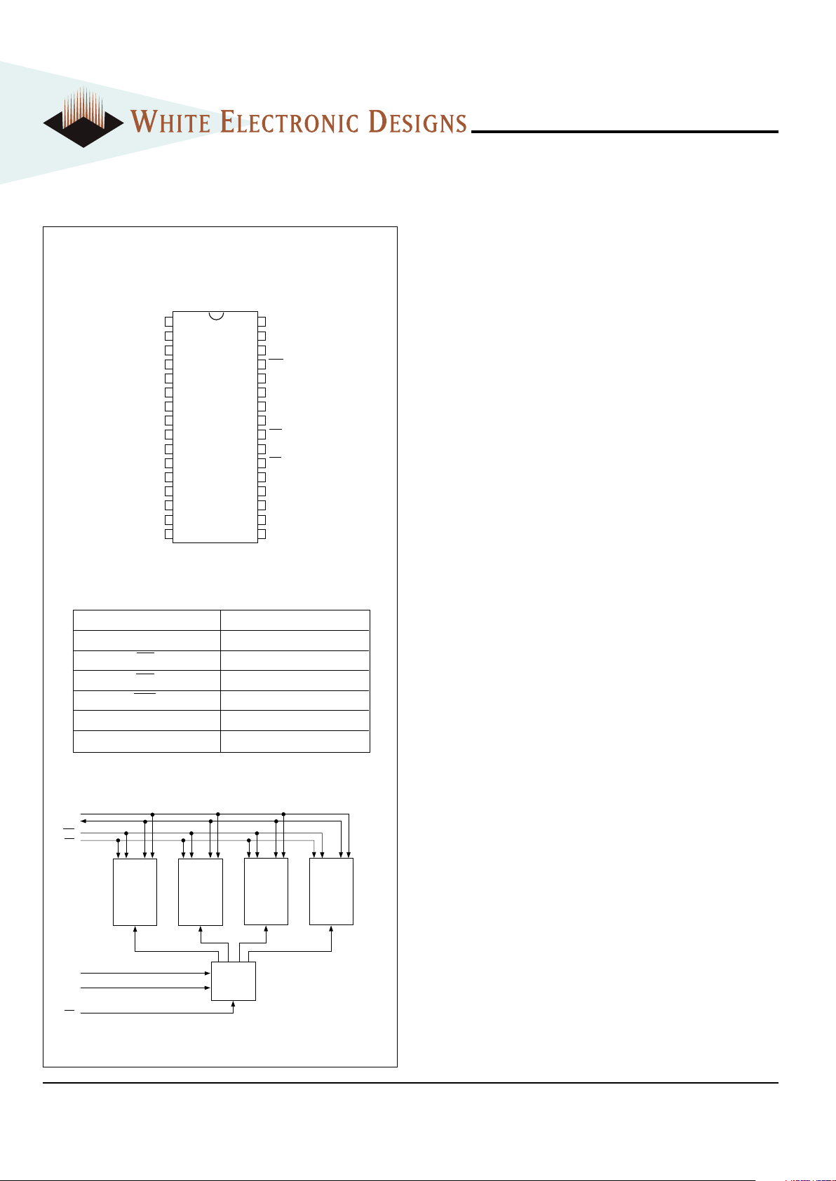
PIN CONFIGURATION
TOP VIEW
FIG. 1
BLOCK DIAGRAM
128K x 8
I/O0-7
128K x 8
128K x 8 128K x 8
A0 -16
OE
Decoder
WE
CS
A17
A18
PIN DESCRIPTION
A0-18 Address Inputs
I/O0-7 Data Input/Output
CS Chip Select
OE Output Enable
WE Write Enable
VCC +5.0V Power
GND Ground
1
2
3
4
5
6
7
8
9
10
11
12
13
14
15
16
32
31
30
29
28
27
26
25
24
23
22
21
20
19
18
17
A18
A16
A14
A12
A7
A6
A5
A4
A3
A2
A1
A0
I/O0
I/O1
I/O2
GND
V
CC
A15
A17
WE
A13
A8
A9
A11
OE
A10
CS
I/O7
I/O6
I/O5
I/O4
I/O3
May 1999 Rev. 2
2
White Electronic Designs Corporation • Phoenix, AZ • (602) 437-1520
WS512K8-XCX
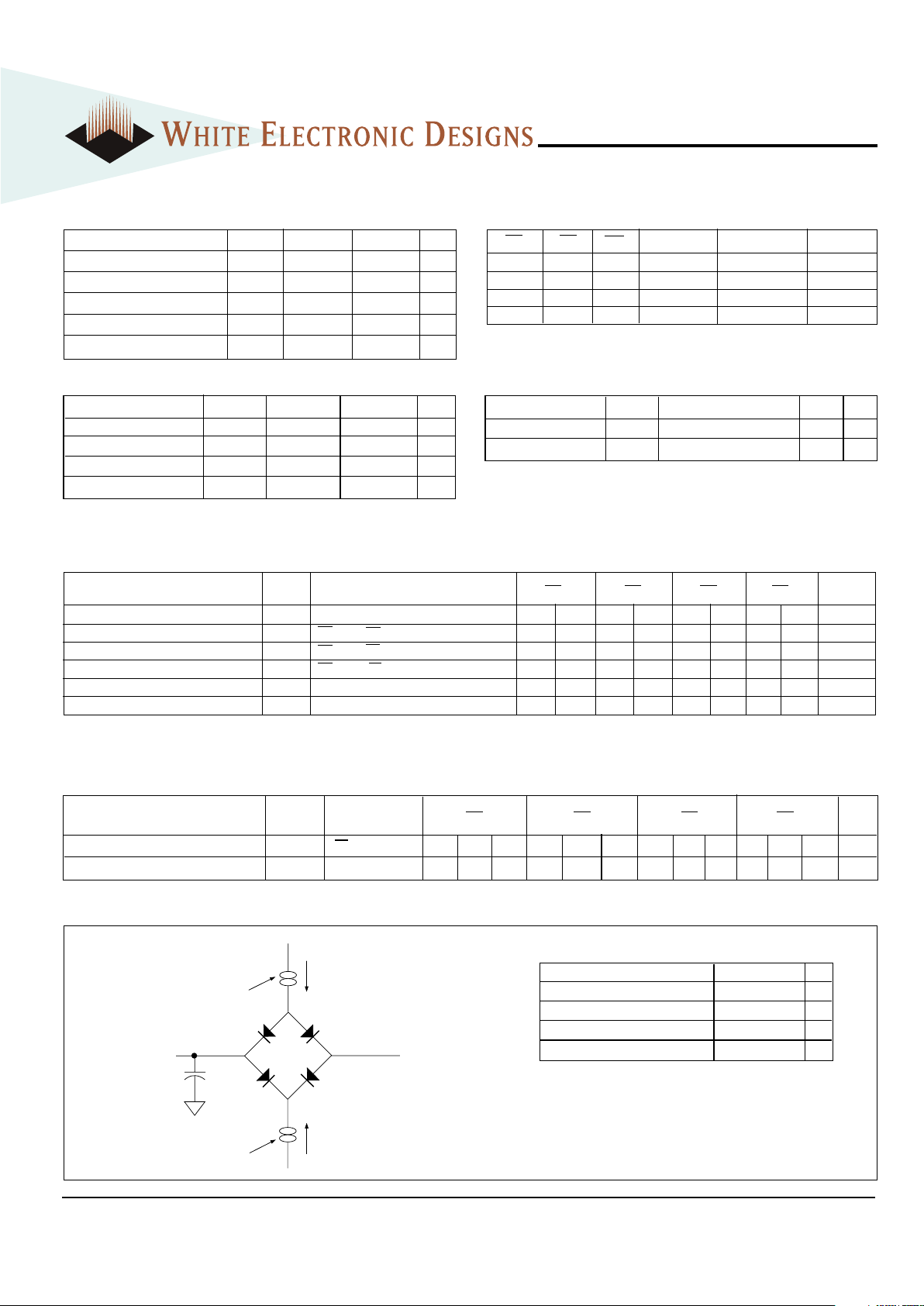
FIG. 2
AC TEST CIRCUIT
I
Current Source
D.U.T.
C = 50 pf
eff
I
OL
V ≈ 1.5V
(Bipolar Supply)
Z
Current Source
OH
TRUTH TABLE
Parameter
Symbol
Condition Max Unit
Input capacitance CIN
VIN = 0V, f = 1.0MHz
45 pF
Output capicitance C
OUT
V
OUT
= 0V, f = 1.0MHz
45 pF
This parameter is guaranteed by design but not tested.
CAPACITANCE
(T
A = +25°C)
AC TEST CONDITIONS
Parameter Typ Unit
Input Pulse Levels VIL = 0, VIH = 3.0 V
Input Rise and Fall 5 ns
Input and Output Reference Level 1.5 V
Output Timing Reference Level 1.5 V
NOTES:
V
Z is programmable from -2V to +7V.
I
OL & IOH programmable from 0 to 16mA.
Tester Impedance Z
0 = 75 Ω.
V
Z is typically the midpoint of VOH and VOL.
I
OL & IOH
are adjusted to simulate a typical resistive load circuit.
ATE tester includes jig capacitance.
ABSOLUTE MAXIMUM RATINGS
Parameter Symbol Min Max Unit
Operating Temperature TA -55 +125 °C
Storage Temperature TSTG -65 +150 °C
Signal Voltage Relative to GND VG -0.5 Vcc+0.5 V
Junction Temperature TJ 150 °C
Supply Voltage V
CC -0.5 7.0 V
RECOMMENDED OPERATING CONDITIONS
Parameter Symbol Min Max Unit
Supply Voltage V
CC 4.5 5.5 V
Input High Voltage V
IH 2.2 VCC + 0.3 V
Input Low Voltage V
IL -0.5 +0.8 V
Operating Temp. (Mil.) T
A -55 +125 °C
CS OE WE Mode Data I/O Power
H X X Standby High Z Standby
L L H Read Data Out Active
L X L Write Data In Active
L H H Out Disable High Z Active
DC CHARACTERISTICS
(VCC = 5.0V, GND = 0V, TA = -55°C to +125°C)
Parameter Symbol Conditions -20 -25 -35 -45 Units
Min Max Min Max Min Max Min Max
Input Leakage Current ILI VCC = 5.5, VIN = GND to VCC 10 10 10 10 µA
Output Leakage Current ILO CS = VIH, OE = VIH, VOUT = GND to VCC 10 10 10 10 µA
Operating Supply Current ICC CS = VIL, OE = VIH, f = 5MHz, Vcc = 5.5 210 210 210 210 mA
Standby Current ISB CS = VIH, OE = VIH, f = 5MHz 80 60 60 55 mA
Output Low Voltage VOL IOL = 8mA, Vcc = 4.5 0.4 0.4 0.4 0.4 V
Output High Voltage V
OH IOH = -4.0mA, Vcc = 4.5 2.4 2.4 2.4 2.4 V
NOTE: DC test conditions: V
IH = VCC -0.3V, VIL = 0.3V
DATA RETENTION CHARACTERISTICS
(TA = -55°C to +125°C)
Parameter Symbol Conditions -20 -25 -35 -45 Units
Min Typ Max Min Typ Max Min Typ Max Min Typ Max
Data Retention Supply Voltage V
DR CS ≥ VCC -0.2V 2.0 5.5 2.0 5.5 2.0 5.5 2.0 5.5 V
Data Retention Current I
CCDR1 VCC = 3V 8.0 12.8 8.0 12.8 8.0 12.8 8.0 12.8 mA
 Loading...