

White Electronic Designs WE32K32N-90G2UIA, WE32K32N-90G2UI, WE32K32N-90G2UCA, WE32K32N-90G2UC, WE32K32N-80H1QA Datasheet
...
1
White Electronic Designs Corporation • Phoenix, AZ • (602) 437-1520
HI-RELIABILITY PRODUCT
WE32K32-XXX
32Kx32 EEPROM MODULE, SMD 5962-94614
FEATURES
■ Access Times of 80*, 90, 120, 150ns
■ MIL-STD-883 Compliant Devices Available
■ Packaging:
• 68 lead, Hermetic CQFP (G2U), 22.4mm (0.880") square,
3.56mm (0.140") height (Package 510). Designed to fit
JEDEC 68 lead 0.990" CQFJ footprint (Fig. 2)
• 66-pin, PGA Type, 1.075" square, Hermetic Ceramic HIP
(Package 400)
■ Data Retention at 25°C, 10 Years
■ Write Endurance, 10,000 Cycles
■ Organized as 32Kx32; User Configurable 64Kx16 or 128Kx8
■ Commercial, Industrial and Military Temperature Ranges
■ Automatic Page Write Operation
■ Page Write Cycle Time: 10ms Max
■ Data Polling for End of Write Detection
■ Hardware and Software Data Protection
■ TTL Compatible Inputs and Outputs
■ 5 Volt Power Supply
■ Low Power CMOS, 10mA Standby Typical
■ Built-in Decoupling Caps and Multiple Ground Pins for Low
Noise Operation
* 80ns speed is not fully characterized and is subject to change or
cancellation without notice.
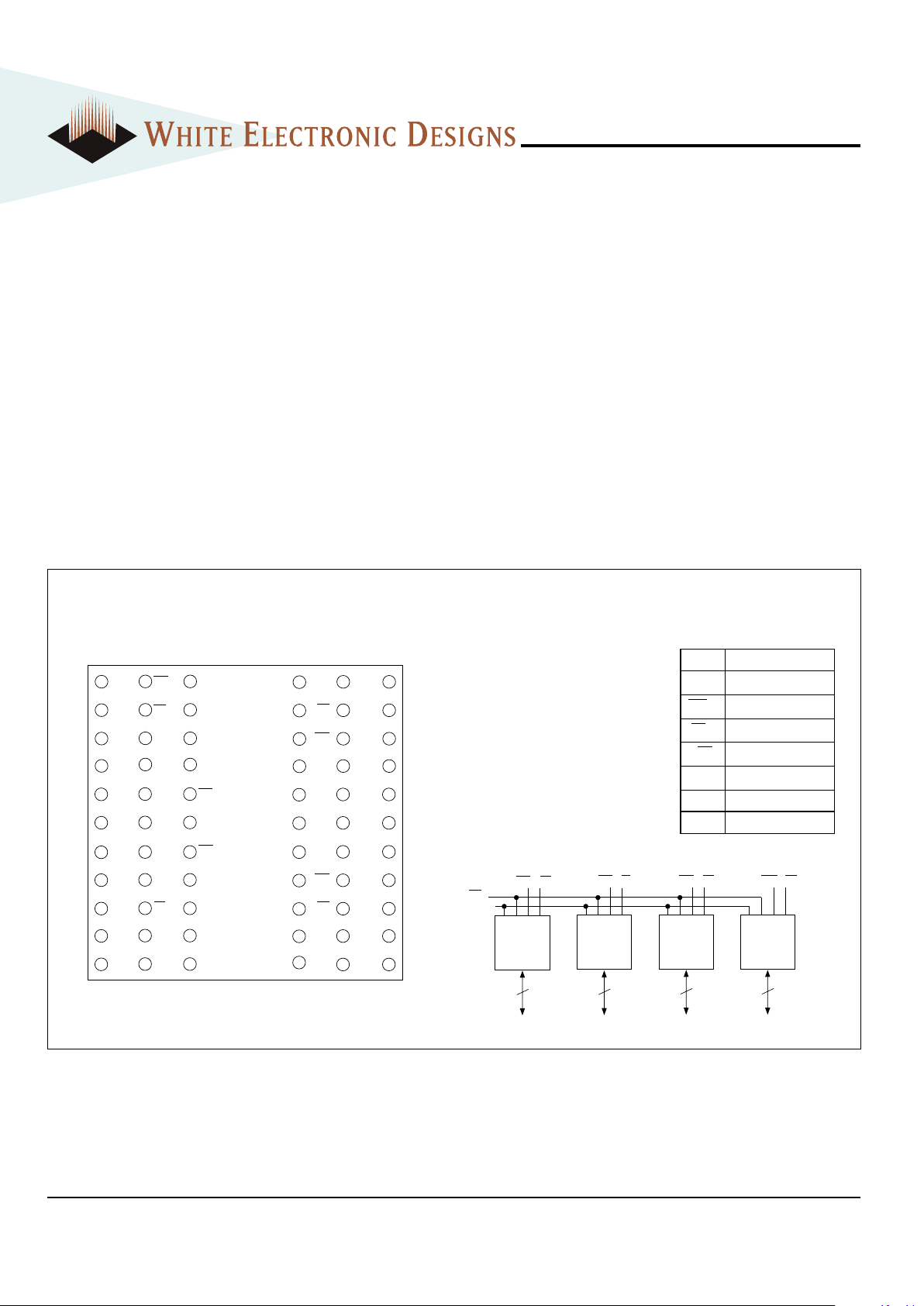
PIN DESCRIPTION
FIG. 1 PIN CONFIGURATION FOR WE32K32N-XH1X
TOP VIEW
I/O8
I/O9
I/O10
A13
A14
NC
NC
NC
I/O
0
I/O1
I/O2
WE2
CS2
GND
I/O
11
A10
A11
A12
VCC
CS1
NC
I/O
3
I/O15
I/O14
I/O13
I/O12
OE
NC
WE
1
I/O7
I/O6
I/O5
I/O4
I/O24
I/O25
I/O26
A6
A7
NC
A
8
A9
I/O16
I/O17
I/O18
VCC
CS4
WE4
I/O27
A3
A4
A5
WE3
CS3
GND
I/O
19
I/O31
I/O30
I/O29
I/O28
A0
A1
A2
I/O23
I/O22
I/O21
I/O20
11 22 33 44 55 66
1 12 23 34 45 56
I/O0-31 Data Inputs/Outputs
A0-14 Address Inputs
WE1-4 Write Enables
CS1-4 Chip Selects
OE Output Enable
VCC Power Supply
GND Ground
NC Not Connected
32K x 8
8
I/O
0-7
WE CS
1
1
32K x 8
8
I/O
8-15
WE CS
2
2
32K x 8
8
I/O
16-23
WE CS
3
3
32K x 8
8
I/O
24-31
WE CS
4
4
A
0-14
OE
BLOCK DIAGRAM
June 1999 Rev. 2
2
White Electronic Designs Corporation • Phoenix, AZ • (602) 437-1520
WE32K32-XXX
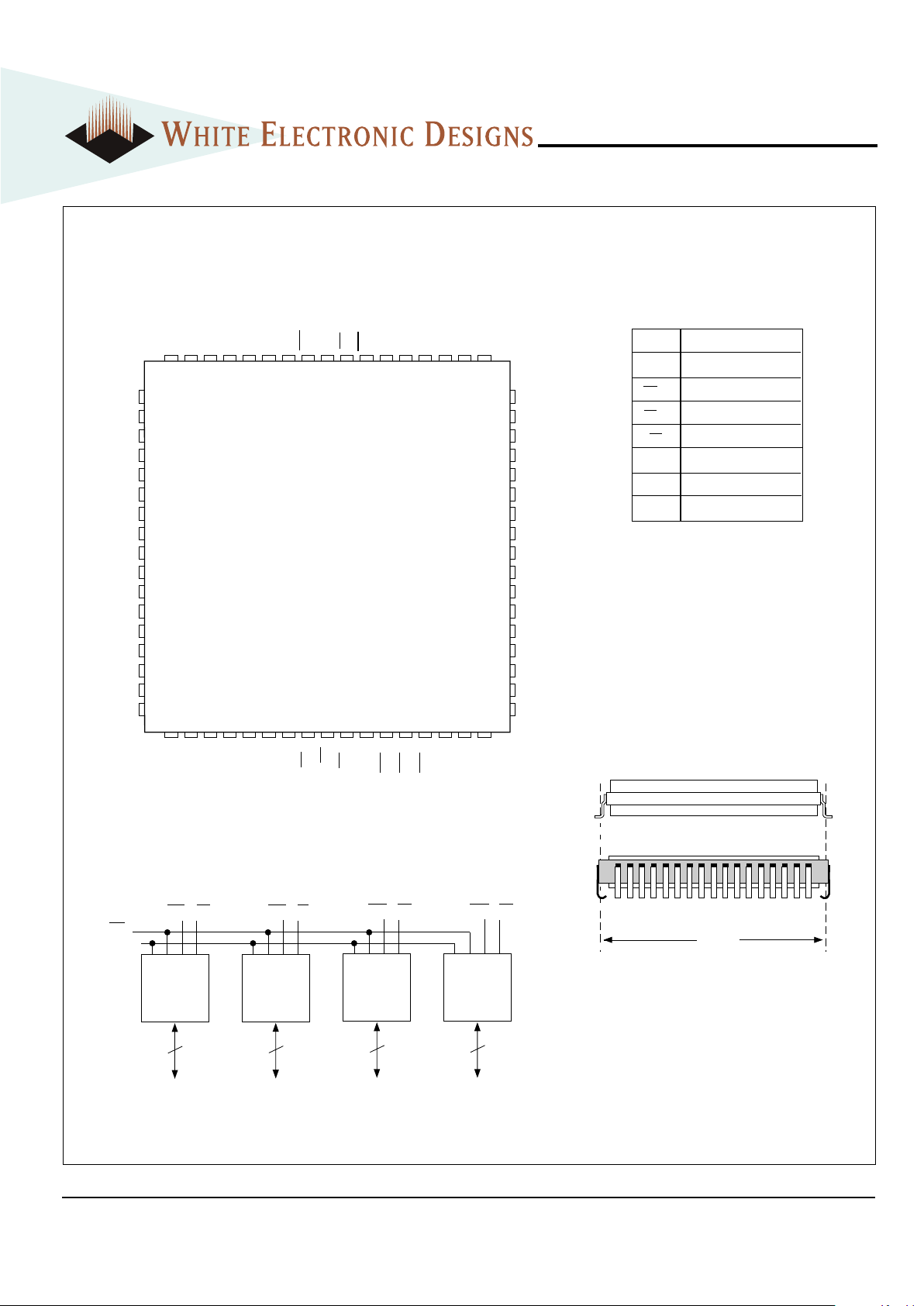
10
11
12
13
14
15
16
17
18
19
20
21
22
23
24
25
26
60
59
58
57
56
55
54
53
52
51
50
49
48
47
46
45
44
9 8 7 6 5 4 3 2 1 68 67 66 65 64 63 62 61
27 28 29 30 31 32 33 34 35 36 37 38 39 40 41 42 43
I/O
0
I/O
1
I/O
2
I/O
3
I/O
4
I/O
5
I/O
6
I/O
7
GND
I/O
8
I/O
9
I/O
10
I/O
11
I/O
12
I/O
13
I/O
14
I/O
15
V
CC
A11A12A13A
14
NC
NC
CS
1
OE
CS
2
NC
WE
2WE3WE4
NC
NC
NC
I/O
16
I/O
17
I/O
18
I/O
19
I/O
20
I/O
21
I/O
22
I/O
23
GND
I/O
24
I/O
25
I/O
26
I/O
27
I/O
28
I/O
29
I/O
30
I/O
31
NC
A0A1A2A3A4A5CS3GND
CS4WE1A6A7A8A9A10V
CC
PIN DESCRIPTION
I/O0-31 Data Inputs/Outputs
A
0-14 Address Inputs
WE1-4 Write Enables
CS1-4 Chip Selects
OE Output Enable
VCC Power Supply
GND Ground
NC Not Connected
FIG. 2 PIN CONFIGURATION FOR WE32K32-XG2UX
BLOCK DIAGRAM
32K x 8
8
I/O
0-7
WE CS
1
1
32K x 8
8
I/O
8-15
WE CS
2
2
32K x 8
8
I/O
16-23
WE CS
3
3
32K x 8
8
I/O
24-31
WE CS
4
4
A
0-14
OE
TOP VIEW
The White 68 lead G2U CQFP
fills the same fit and function as
the JEDEC 68 lead CQFJ or 68
PLCC. But the G2U has the TCE
and lead inspection advantage
of the CQFP form.
0.940"
3
White Electronic Designs Corporation • Phoenix, AZ • (602) 437-1520
WE32K32-XXX
ABSOLUTE MAXIMUM RATINGS
DC CHARACTERISTICS
(V
CC = 5.0V, GND = 0V, TA = -55°C to +125°C)
TRUTH TABLE
NOTE:
Stresses above those listed under "Absolute Maximum Ratings" may cause
permanent damage to the device. This is a stress rating only and functional
operation of the device at these or any other conditions above those indicated in
the operational sections of this specification is not implied. Exposure to
absolute maximum rating conditions for extended periods may affect device
reliability.
RECOMMENDED OPERATING CONDITIONS
CAPACITANCE
(T
A = 25° C)
FIG. 3
AC TEST CIRCUIT
AC TEST CONDITIONS
I
Current Source
D.U.T.
C = 50 pf
eff
I
OL
V ≈ 1.5V
(Bipolar Supply)
Z
Current Source
OH
NOTES:
V
Z is programmable from -2V to +7V.
I
OL & IOH programmable from 0 to 16mA.
Tester Impedance Z
0 = 75 Ω.
V
Z is typically the midpoint of VOH and VOL.
I
OL & IOH
are adjusted to simulate a typical resistive load circuit.
ATE tester includes jig capacitance.
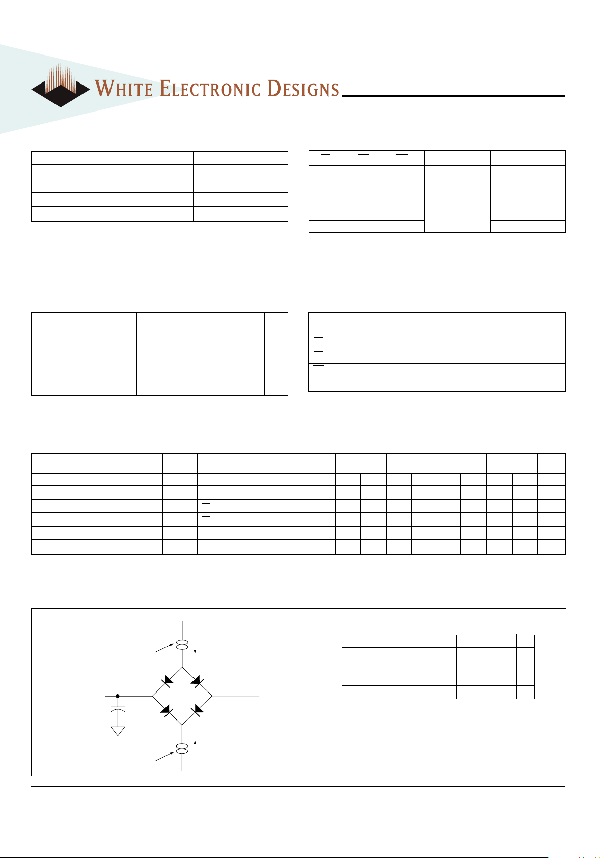
CS OE WE Mode Data I/O
H X X Standby High Z
L L H Read Data Out
L H L Write Data In
X H X Out Disable High Z/Data Out
X X H Write
X L X Inhibit
Parameter Symbol Unit
Operating Temperature TA -55 to +125 °C
Storage Temperature TSTG -65 to +150 °C
Signal Voltage Relative to GND VG -0.6 to +6.25 V
Voltage on OE and A9 -0.6 to +13.5 V
Parameter Symbol Min Max Unit
Supply Voltage VCC 4.5 5.5 V
Input High Voltage VIH 2.0 VCC + 0.3 V
Input Low Voltage VIL -0.5 +0.8 V
Operating Temp. (Mil.) TA -55 +125 °C
Operating Temp. (Ind.) T
A -40 +85 °C
Parameter Symbol Condition Max Unit
Address Input Capacitance C
AD VIN = 0V, f = 1.0MHz 50 pF
OE Capacitance COE
CS1-4 Capacitance CCS VIN = 0V, f = 1.0MHz 20 pF
WE1-4 Capacitance CWE VIN = 0V, f = 1.0MHz 20 pF
Data I/
O
Capacitance CI/O VIN = 0V, f = 1.0MHz 20 pF
This parameter is guaranteed by design but not tested.
Parameter Symbol Conditions -80 -90 -120 -150 Units
Min Max Min Max Min Max Min Max
Input Leakage Current ILI VCC = 5.5, VIN = GND to VCC 10 10 10 10 µA
Output Leakage Current ILO x 32 CS = VIH, OE = VIH, VOUT = GND to VCC 10 10 10 10 µA
Operating Supply Current x 32 Mode ICC x 32 CS = VIL, OE = VIH, f = 5MHz 320 250 200 150 mA
Standby Current ISB CS = VIH, OE = V IH, f = 5MHz 2.5 2.5 2.5 2.5 mA
Output Low Voltage VOL IOL = 2.1mA, VCC = 4.5V 0.45 0.45 0.45 0.45 V
Output High Voltage V
OH IOH = -400µA, VCC = 4.5V 2.4 2.4 2.4 2.4 V
NOTE: DC test conditions: V
IH = VCC -0.3V, VIL = 0.3V
Parameter Typ Unit
Input Pulse Levels VIL = 0, VIH = 3.0 V
Input Rise and Fall 5 ns
Input and Output Reference Level 1.5 V
Output Timing Reference Level 1.5 V
4
White Electronic Designs Corporation • Phoenix, AZ • (602) 437-1520
WE32K32-XXX
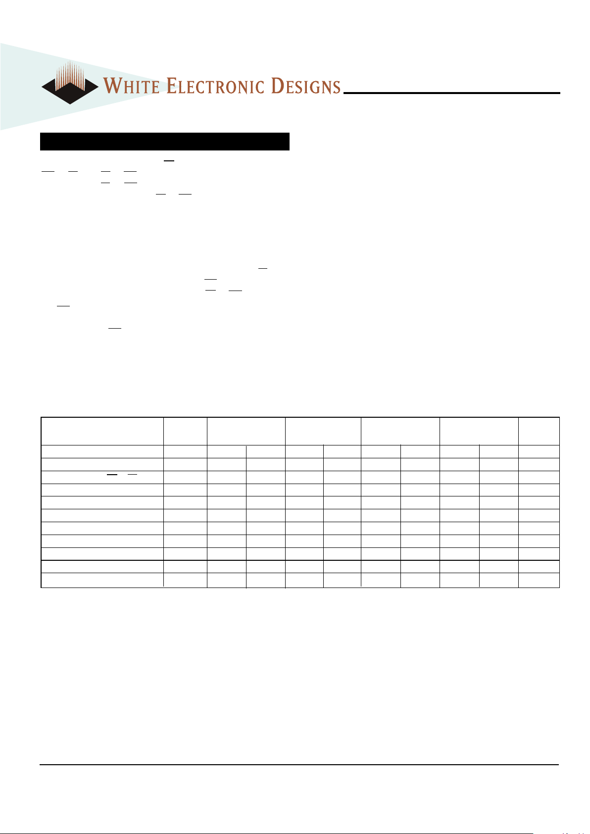
A write cycle is initiated when OE is high and a low pulse is on
WE or CS with CS or WE low. The address is latched on the
falling edge of CS or WE whichever occurs last. The data is
latched by the rising edge of CS or WE, whichever occurs first.
A byte write operation will automatically continue to completion.
WRITE
WRITE CYCLE TIMING
Figures 4 and 5 show the write cycle timing relationships. A
write cycle begins with address application, write enable and
chip select. Chip select is accomplished by placing the CS line
low. Write enable consists of setting the WE line low. The
write cycle begins when the last of either CS or WE goes low.
The WE line transition from high to low also initiates an
internal 150 µsec delay timer to permit page mode operation.
Each subsequent WE transition from high to low that occurs
before the completion of the 150 µsec time out will restart the
timer from zero. The operation of the timer is the same as a
retriggerable one-shot.
AC WRITE CHARACTERISTICS
(V
CC
= 5.0V, GND = 0V, TA = -55°C to +125°C)
WRITE CYCLE -80 -90 -120 -150
Write Cycle Parameter Symbol Min Max Min Max Min Max Min Max Unit
Write Cycle Time, TYP = 6ms tWC 10 10 10 10 ms
Address Set-up Time tAS 0 0 30 30 ns
Write Pulse Width (WE or CS) tWP 100 100 150 150 ns
Chip Select Set-up Time tCS 000 0ns
Address Hold Time tAH 50 50 100 100 ns
Data Hold Time tDH 0 0 10 10 ns
Chip Select Hold Time tCSH 000 0ns
Data Set-up Time tDS 50 50 100 100 ns
Write Pulse Width High tWPH 50 50 50 50 ns
Output Enable Set-up Time tOES 10 10 10 10 ns
Output Enable Hold Time t
OEH 10 10 10 10 ns
 Loading...