

Page 1

查询WT6148供应商
Weltrend Semiconductor, Inc.
WT6148/WT6160
Digital Monitor Controller
(ROM Type)
Preliminary Data Sheet
REV. 1.02
Sep. 4, 02
The information in this document is subject to change without notice.
Weltrend Semiconductor, Inc. All Rights Reserved.
Page 2
WT6148/WT6160v1.02
Digital Monitor Controller
GENERAL DESCRIPTION
The WT6148/ WT6160 is a microcontroller for digital controlled monitor. It contains an 8-bit CPU, 48K
/60K bytes ROM, 1056 bytes RAM, 14 PWMs, parallel I/Os, SYNC signal processor, timer, DDC1/2B
interface, master/slave I2C interface, 6-bit A/D converter and watch-dog timer.
FEATURES
• 8-bit 6502 compatible CPU with 6MHz operating frequency
• WT6148 : 48K bytes ROM,
WT6160 : 60K bytes ROM,
,1024 bytes SRAM+32 bytes bit addressable SRAM
• 12MHz crystal oscillator
• 14 channels 8-bit PWM outputs
• Sync signal processor with H+V separation, H/V frequency counter, H/V polarity detection/control
and clamp pulse output
• Six free-running sync signal outputs (Horizontal frequency up to 106KHz 85Hz@1600x1200)
• Self-test pattern
• DDC1/2B module for EDID1.3, EDID2.0 and Enhance EDID
• Fast mode master/slave I2C interface (up to 400KHz)
• Watch-dog timer
• Maximum 28 programmable I/O pins
• One 8-bit programmable timer
• 6-bit A/D converter with 4 selectable inputs
• One external interrupt request input
• Low VDD reset
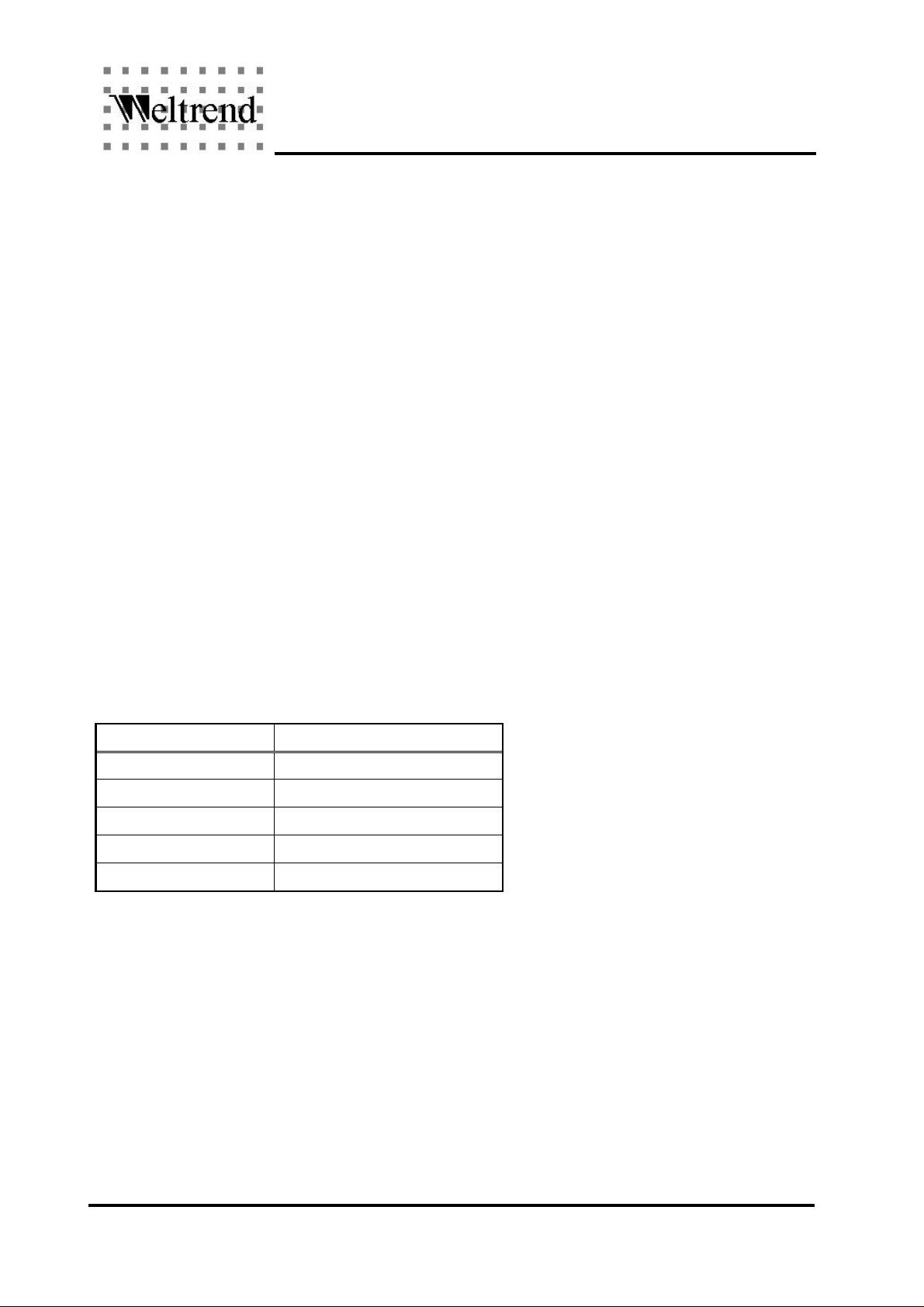
ORDERING INFORMATION
Package Type Part Number
42-pin PDIP WT6148/ WT6160-N42
42-pin Shrink PDIP WT6148/ WT6160-K42
40-pin PDIP WT6148/ WT6160-N40
44-pin SOP WT6148/ WT6160-S44
44-pin PLCC WT6148/ WT6160-L44
Weltrend Semiconductor, Inc.
Page 2
Page 3

PIN ASSIGNMENT AND PACKAGE TYPE
42-pin SPDIP
42
41
VIN
40
HIN
39
PWM3
38
PD5/PWM4
37
PD4/PWM5
36
PD3/PWM6
35
PD2/PWM7
34
PD1/HOUT
33
PD0/VOUT
32
PA7/PWM13/CLAMP
31
PA6/PWM12
30
PA5/PWM11
29
PA4/PWM10
28
PA3/PWM9
27
PA2/PWM8
26
PA1/SCL1
25
PA0/SDA1
24
PC0/AD0
23
PC1/AD1
2221
PC2/AD2PC3/AD3
PWM2
PWM1
PWM0
RESET/3V3
OSCO
PB5/SDA2
PB4/SCL2
PB3/PAT
PB1/HFI
PB0/HFO
PC7/SOGIN
PWM2
PWM1
PWM0
RESET/3V3
VDD
GND
OSCO
OSCI
PB5/SDA2
PB4/SCL2
PB3/PAT
PB2
PB1/HFI
PB0/HFO
IRQ
PC7/SOGIN
PC6
PC5
PC4
1
2
3
4
5
6
7
8
9
10
11
12
13
14
15
16
17
18
19
20
WT6148-K42
WT6160-K42
WT6148/WT6160v1.02
Digital Monitor Controller
40-pin PDIP
40
VIN
39
HIN
38
PWM3
37
PD5/PWM4
36
PD4/PWM5
35
PD3/PWM6
34
PD2/PWM7
33
PD1/HOUT
32
PD0/VOUT
31
PA7/PWM13/CLAMP
30
PA6/PWM12
29
PA5/PWM11
28
PA4/PWM10
27
PA3/PWM9
26
PA2/PWM8
25
PA1/SCL1
24
PA0/SDA1
23
PC0/AD0
22
PC1/AD1
21
PC2/AD2PC3/AD3
VDD
GND
OSCI
PB2
IRQ
PC6
PC5
PC4
1
2
3
4
5
6
7
8
9
10
11
12
13
14
15
16
17
18
19
20
WT6148-N40
WT6160-N40
RESET/3V3
PB5/SDA2
PB4/SCL2
PB3/PAT
PB1/HFI
PB0/HFO
PC7/SOGIN
PWM2
PWM1
PWM0
VDD
GND
OSCO
OSCI
PB2
IRQ
PC6
PC5
PC4
1
2
3
4
5
6
7
8
9
10
11
12
13
14
15
16
17
18
19
20
21
44-pin SOP
WT6148-S44
WT6160-S44
44
43
VIN
42
HIN
41
PWM3
40
PD5/PWM4
39
PD4/PWM5
38
37
PD3/PWM6
36
PD2/PWM7
35
PD1/HOUT
34
PD0/VOUT
33
PA7/PWM13/CLAMP
32
PA6/PWM12
31
PA5/PWM11
30
PA4/PWM10
29
PA3/PWM9
28
PA2/PWM8
27
PA1/SCL1
26
PA0/SDA1
25
PC0/AD0
24
PC1/AD1
2322
PC2/AD2PC3/AD3
VDD
OSCO
OSCI
PB5/SDA2
PB4/SCL2
PB3/PAT
PB2
PB1/HFI
PB0/HFO
IRQ
RESET/3V3
65432
7
8GND
9
10
11
12
13
14
15
16
17
19
18
PC6
PC7/SOGIN
44-pin PLCC
PWM0
PWM1
PWM2
1
WT6148-L44
WT6160-L44
23
22
21
20
PC4
PC5
PC2/AD2
PC3/AD3
HIN
VIN
4443424140
27
26
25
24
PC0/AD0
PC1/AD1
PA0/SDA1
PA1/SCL1
PWM3
39
PD5/PWM4
38
PD4/PWM5
37
PD3/PWM6
36
PD2/PWM7
35
PD1/HOUT
34
PD0/VOUT
33
PA7/PWM13/CLAMP
32
PA6/PWM12
31
PA5/PWM11
30
PA4/PWM10
29
PA3/PWM9
28
PA2/PWM8
Weltrend Semiconductor, Inc.
Page 3
Page 4

Interrupt request input. A low level on this can generate
PIN DESCRIPTION
Pin No. Pin Name I/O Description
L44 S44 42 40
1 1 1 - NC No Connection.
2 2 2 1 PWM2 O PWM2 output (10V open-drain).
3 3 3 2 PWM1 O PWM1 output (5V open-drain).
4 4 4 3 PWM0 O PWM0 output (5V open-drain).
5 5 5 4 /RESET I Reset input
6 - - - NC No Connection.
7 6 6 5 VDD +5V power supply.
- 7 - - NC No Connection.
8 8 7 6 GND Ground.
9 9 8 7 OSCO I/O 12MHz oscillator output.
10 10 9 8 OSCI I 12MHz oscillator input.
11 11 10 9 PB5/ SDA2 I/O Port B5 or I2C interface data line.
12 12 11 10 PB4/ SCL2 I/O Port B4 or I2C interface clock line.
13 13 12 11 PB3/PAT I/O Port B3 or test pattern output
14 14 13 12 PB2 I/O Port B2.
15 15 14 13 PB1/HFI I/O Port B1 or half frequency divider input.
16 16 15 14 PB0/HFO I/O Port B0 or half frequency divider output.
17 17 16 15 /IRQ I
18 18 17 6 PC7/SOGIN I/O Port C7 or Sync on Green input.
19 19 18 17 PC6 I/O Port C6.
20 20 19 18 PC5 I/O Port C5.
21 21 20 19 PC4 I/O Port C4.
22 22 21 20 PC3/AD3 I/O Port C3 or ADC input 3.
23 23 22 21 PC2/AD2 I/O Port C2 or ADC input 2.
24 24 23 22 PC1/AD1 I/O Port C1 or ADC input 1.
25 25 24 23 PC0/AD0 I/O Port C0 or ADC input 0.
26 26 25 24 PA0/SDA1 I/O Port A0 or DDC interface SDA pin.
27 27 26 25 PA1/SCL1 I/O Port A1 or DDC interface SCL pin.
28 28 27 26 PA2/PWM8 I/O Port A2 or PWM8 output.
29 29 28 27 PA3/PWM9 I/O Port A3 or PWM9 output.
30 30 29 28 PA4/PWM10 I/O Port A4 or PWM10 output.
31 31 30 29 PA5/PWM11 I/O Port A5 or PWM11 output.
32 32 31 30 PA6/PWM12 I/O Port A6 or PWM12 output.
33 33 32 31 PA7/PWM13/
CLAMP
34 34 33 32 PD0/VOUT I/O Port D0 or Vsync output.
35 35 34 33 PD1/HOUT I/O Port D1 or Hsync output.
36 36 35 34 PD2/PWM7 I/O Port D2 or PWM7 output.
37 37 36 35 PD3/PWM6 I/O Port D3 or PWM6 output.
- 38 - - NC No Connection.
38 39 37 36 PD4/PWM5 I/O Port D4 or PWM5 output.
39 40 38 37 PD5/PWM4 I/O Port D5 or PWM4 output.
40 41 39 38 PWM3 I/O PWM3 output (10V open-drain).
41 42 40 39 HIN I Hsync Input.
42 43 41 40 VIN I Vsync input.
interrupt.
I/O Port A7 or PWM13 output or clamp pulse output.
WT6148/WT6160v1.02
Digital Monitor Controller
Weltrend Semiconductor, Inc.
Page 4
Page 5

WT6148/WT6160v1.02
Digital Monitor Controller
43 - - - NC No Connection.
44 44 42 - NC No Connection.
FUNCTIONAL DESCRIPTION
CPU
8-bit 6502 compatible CPU operates at 6MHz. Address bus is 16-bit and data bus is 8-bit.
The non-maskable interrupt (/NMI) of 6502 is modified to be maskable and is defined as INT0 with higher
priority. The interrupt request (/IRQ) of 6502 is defined as INT1 with lower priority.
Please refer the 6502 reference menu for more detail.
RAM
The 1024 bytes SRAM include :
128 bytes SRAM are from $0080H to $00FFH
256 bytes SRAM are from $0100H to $01FFH
256 bytes SRAM are from $0200H to $02FFH
256 bytes SRAM are from $0300H to $03FFH
128 bytes SRAM are from $0400H to $047FH
The 32 bytes SRAM bit addressible are from $0500H to $05FFH
ROM
For WT6148, ROM address is located from $4000h to $FFFFh.
For WT6160, ROM address is located from $1000h to $FFFFh.
The following addresses are reserved for special purpose :
$FFFAh (low byte) and $FFFBh (high byte) : INT0 interrupt vector.
$FFFCh (low byte) and $FFFDh (high byte) : program reset interrupt vector.
$FFFEh (low byte) and $FFFFh (high byte) : INT1 interrupt vector.
Weltrend Semiconductor, Inc.
Page 5
 Loading...