

Page 1
偉詮電子股份有限公司
Weltrend Semiconductor, Inc.
WT6248
Digital Monitor Controller with USB Function
(ROM Type)
Preliminary Data Sheet
REV. 1.0
Feb. 29, 2000
The information in this document is subject to change without notice.
Weltrend Semiconductor, Inc. All Rights Reserved.
新竹市科學工業園區工業東九路 24 號2 樓
2F, No. 24, Industry E. 9th RD., Science-Based Industrial Park, Hsin-Chu, Taiwan
TEL:886-3-5780241 FAX:886-3-5794278.5770419
Email:[email protected]
Page 2
WT6248v1.0
USB Monitor Controller
GENERAL DESCRIPTION
The WT6248 is a microcontroller for digital controlled monitor with Universal Serial Bus (USB) interface. It
contains an 8-bit CPU, 48K bytes ROM, 1056 bytes RAM, 14 PWMs, parallel I/Os, SYNC signal processor,
timer, DDC1/2B interface, master/slave I2C interface, low speed USB device module, 6-bit A/D converter and
watch-dog timer.
FEATURES
• 8-bit 6502 compatible CPU with 6MHz operating frequency
• 48K bytes ROM, 1024 bytes SRAM+32 bytes bit addressible SRAM
• 12MHz cry stal oscillator
• 14 channels 8-bit PWM outputs
• Sync signal processor with H+V separation, H/V frequency counter, H/V polarity detection/control and
clamp pulse output
• Six free-running sync signal outputs (Horizontal frequency up to 106KHz)
• Self-test pattern
• DDC1/2B supported
• Fast mode master/slave I2C interface (up to 400KHz)
• Embedded USB function with endpoint 0 and endpoint 1
• Built-in 3.3V regulator for USB transceiver
• Watch-dog timer
• Maximum 28 programmable I/O pins
• One 8-bit programmable timer
• 6-bit A/D converter with 4 selectable inputs
• One external interrupt request input
• Low VDD reset
ORDERING INFORMATION
Package Type Part Number
42-pin PDIP WT6248-N42
42-pin Shrink PDIP WT6248-K42
44-pin SOP WT6248-S44
Weltrend Semiconductor, Inc.
Page 2
Page 3
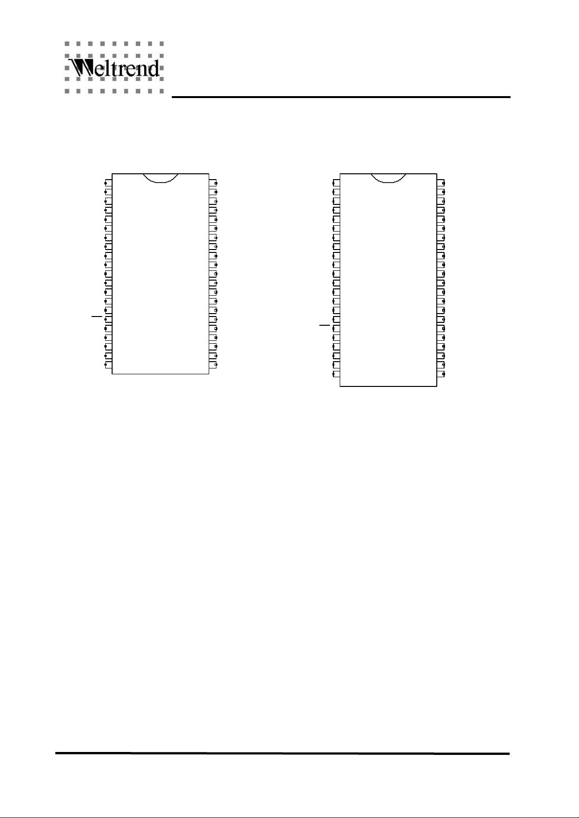
PIN CONFIGURATION
Shrink DIP 42-pin
DIP 42-pin
1
D+ D-
VDD
GND
OSCI
PB2
IRQ
PC6
PC5
PC4
2
3
4
5
6
7
8
9
10
WT6248 WT6248
11
12
13
14
15
16
17
18
19
20
PWM2
PWM1
PWM0
RESET/3V3
OSCO
PB5/SDA2
PB4/SCL2
PB3/PAT
PB1/HFI
PB0/HFO
PC7/SOGIN
42
41
40
39
38
37
36
35
34
33
32
31
30
29
28
27
26
25
24
23
2221
VIN
HIN
PWM3
PD5/PWM4
PD4/PWM5
PD3/PWM6
PD2/PWM7
PD1/HOUT
PD0/VOUT
PA7/PWM13/CLAMP
PA6/PWM12
PA5/PWM11
PA4/PWM10
PA3/PWM9
PA2/PWM8
PA1/SCL1
PA0/SDA1
PC0/AD0
PC1/AD1
PC2/AD2PC3/AD3
USB Monitor Controller
SOP 44-pin
1
D+ D-
VDD
GND
OSCI
PB2
IRQ
PC6
PC5
PC4
2
3
4
5
6
7
8
9
10
11
12
13
14
15
16
17
18
19
20
21
PWM2
PWM1
PWM0
RESET/3V3
OSCO
PB5/SDA2
PB4/SCL2
PB3/PAT
PB1/HFI
PB0/HFO
PC7/SOGIN
WT6248v1.0
44
43
VIN
42
HIN
41
PWM3
40
PD5/PWM4
39
PD4/PWM5
38
37
PD3/PWM6
36
PD2/PWM7
35
PD1/HOUT
34
PD0/VOUT
33
PA7/PWM13/CLAMP
32
PA6/PWM12
31
PA5/PWM11
30
PA4/PWM10
29
PA3/PWM9
28
PA2/PWM8
27
PA1/SCL1
26
PA0/SDA1
25
PC0/AD0
24
PC1/AD1
2322
PC2/AD2PC3/AD3
Weltrend Semiconductor, Inc.
Page 3
Page 4
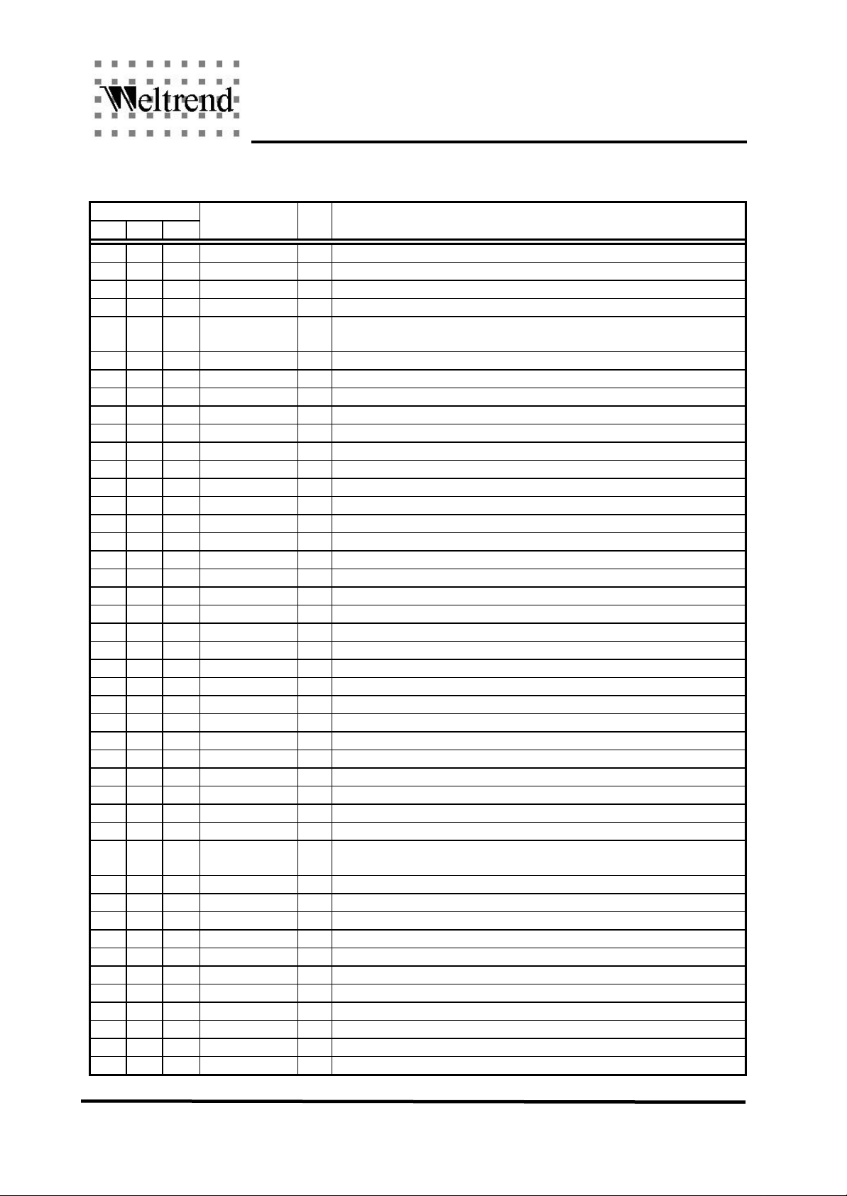
PIN DESCRIPTION
WT6248v1.0
USB Monitor Controller
Pin No.
44 42 40
1 1 - D+ I/O USB D+ signal.
2 2 1 PWM2 O PWM2 output (10V open-drain).
3 3 2 PWM1 O PWM1 output (5V open-drain).
4 4 3 PWM0 O PWM0 output (5V open-drain).
5 5 4 /RESET/3V3 I Reset input and +3.3V regulator output for USB transceiver power
6 6 5 VDD +5V power supply.
7 - - NC No Connection.
8 7 6 GND Ground.
9 8 7 OSCO I/O 12MHz oscillator output.
10 9 8 OSCI I 12MHz oscillator input.
11 10 9 PB5/ SDA2 I/O Port B5 or I2C interface data line.
12 11 10 PB4/ SCL2 I/O Port B4 or I2C interface clock line.
13 12 11 PB3/PAT I/O Port B3 or test pattern output
14 13 12 PB2 I/O Port B2.
15 14 13 PB1/HFI I/O Port B1 or half frequency divider input.
16 15 14 PB0/HFO I/O Port B0 or half frequency divider output.
17 16 15 /IRQ I Interrupt request input. A low level on this can generate interrupt.
18 17 6 PC7/SOGIN I/O Port C7 or Sync on Green input.
19 18 17 PC6 I/O Port C6.
20 19 18 PC5 I/O Port C5.
21 20 19 PC4 I/O Port C4.
22 21 20 PC3/AD3 I/O Port C3 or ADC input 3.
23 22 21 PC2/AD2 I/O Port C2 or ADC input 2.
24 23 22 PC1/AD1 I/O Port C1 or ADC input 1.
25 24 23 PC0/AD0 I/O Port C0 or ADC input 0.
26 25 24 PA0/SDA1 I/O Port A0 or DDC interface SDA pin.
27 26 25 PA1/SCL1 I/O Port A1 or DDC interface SCL pin.
28 27 26 PA2/PWM8 I/O Port A2 or PWM8 output.
29 28 27 PA3/PWM9 I/O Port A3 or PWM9 output.
30 29 28 PA4/PWM10 I/O Port A4 or PWM10 output.
31 30 29 PA5/PWM11 I/O Port A5 or PWM11 output.
32 31 30 PA6/PWM12 I/O Port A6 or PWM12 output.
33 32 31 PA7/PWM13/
34 33 32 PD0/VOUT I/O Port D0 or Vsync output.
35 34 33 PD1/HOUT I/O Port D1 or Hsync output.
36 35 34 PD2/PWM7 I/O Port D2 or PWM7 output.
37 36 35 PD3/PWM6 I/O Port D3 or PWM6 output.
38 - - NC No Connection.
39 37 36 PD4/PWM5 I/O Port D4 or PWM5 output.
40 38 37 PD5/PWM4 I/O Port D5 or PWM4 output.
41 39 38 PWM3 I/O PWM3 output (10V open-drain).
42 40 39 HIN I Hsync Input.
43 41 40 VIN I Vsync input.
44 42 - D- I/O USB D- signal.
Pin Name I/O Description
supply.
I/O Port A7 or PWM13 output or clamp pulse output.
CLAMP
Weltrend Semiconductor, Inc.
Page 4
Page 5
WT6248v1.0
USB Monitor Controller
Weltrend Semiconductor, Inc.
Page 5
 Loading...