

Page 1
INSTRUCTION
MANUAL
9045
BALBOA
AVENUE
SAN
DIEGO,
.
CALIFORNIA
Page 2
N
Y
All
Wavetek
of
one
component
Wavetek'sobligation
Wavetek's
to the
to
is
Wavetek
This
warranty
Wavetek,
defectiveasa
be
billedatcost
Wavetek
either
be
dangerous
liability
breach
specific
Any
recommendations
reliable,
all
other
represent or
than
set
instruments
year
after
(except
opinion
sole
factory or toanauthorized
be
prepaid
.
does
or
notinaccordance
result
.
assumes
aloneorin
if
misused
for
secondary
of
warranty
instrument
Wavetek
but
warranties,
assume
forth herein
are
warranteed
date
of
manufacture
batteries)
under
proves
by
purchaser
not
misuse,
of
no
responsibility
conjunction
chargesorconsequential
under
shipped
made
makes
expressed
for
.
found
this
warranty
to
.
Shipment
to
apply
with
improper
with
Special
.
any
contractorotherwise,
and
against
by
Wavetek
no
warrantyofthe
or
Wavetek
any
against
to
is
defective
be
service
any
products
instructions
for
its
other
disclaimers
which
for use of
implied,
liabilityinconnection
defects
.
Wavetek
be
defective,
limited
within
center.Transportation
should
repaired
repair,
or
product
equipment
apply
damages
a claim
and
in
agrees
under
to
solely
the
not
be
or
furnished
abnormal
being
used
High
.
these
to
and,inany
shall
is
made
its
products
resultstobe
no
representative or
material
to
repairing
scope
made
alteredbypersons
voltage
and
workmanship
repairorreplace
normal
by
conditions
in a
instruments.Wavetek
not exceed
.
are
obtained.Thiswarranty
with
use,
any
such
the
warranty
of
to the
factory
without
Wavetek.If
hazardousordangerous
based
the
prior
or operations,
usedinsome
event,
Wavetek's
the
purchase
upon
person
sale
of
any
during
instrument
when
service
or
authorization
authorized
not
instrument
the
instruments
believed to be
tests
is
authorized
our
products
foraperiod
assembly
this
period
which
returned
center
repairs
will
manner
may
assumes
liability
price
of the
isinlieu
other
or
.
in
by
by
is
no
for
of
to
Page 3
Wavetek
will
maintainsacontinuing
take
advantage
of the
latest
program
electronic
to
make
developments
improvements
in
circuitry
to
their
instruments
components
and
that
.
Due
possibletoincorporate
Wavetek
of
the
the
and
If
in
the
the
to
5%
carbon
overall
resistor
Schematic
field
replacernent
accordance
same
has
performance
type of
required
time
manufactured
resistors,
usedtomanufacture
Diagramsinthis
with
resistor
of an
the
to
these
changesinthe
your
wherever
of
your
affected
manual
usedinthe
document
instrument,
practical.This
instrument.Therefore,
your
manual
resistor
call
and
manual
using
instrument
.
does
become
outs.Wavetek,
manufacture
print
and
instruction
.
metal
results
there
the
however,
of
film
1%
in a
may
resistor
necessary,
recommends
your
instrument,
manuals,
tolerance
substantial
existadiscrepancy
called
replacement
it is
resistorsinplace
improvement
outinthe
may
replacement
whenever
not always
between
Parts
List
be
made
with
possible
in
.
Page 4

Page 5
Section1GENERAL
DESCRIPTION
ScopeofManual
ScopeofEquipment
ModesofOperation
Remote
Functional
Specifications.. . . .
Section2OPERATING
Installation
Inspection
Manual
Programming
Section3CIRCUIT
Introduction
Program
Basic
Generator
Low-Frequency
Sine
Conversion
"tone
Burst
Power
Supply
.
Control
Operation
Selection
Operation
Descriptions..
INSTRUCTIONS
.
. .
. ... ...
. . . .
DESCRIPTION
. . . . ... ... . ..... . . . . . . . . . . . . . ... . ... .
. ... . . . ... ... . . . ... . . . ... . . . . . . . . . . .
Generator
. ... . . . . . . ... ... ... ... ... . . . . . . . . . . .
Generation
..... . . . . . . . . . ... . . . ... . . . . ... . ... . . .
. ... ... . . . ... ... ... ... . . . . ... ... . ..1-1
... ... . . . ... ... .
.
. .
. . . . . . . . . . . . . . . ... . ... ... . ... . .
. . ... ... . . . ... ... ... ... ... . ... . .
. ... ... ... ... ... ... .
. .
. ..... . . . ... ... . ... ... . . . . . . . .
. ... ... . . . ... . . ... . . . . ... . . . . ... .
... ... ... . . .
. ... ... . . . ... ... ... . . . .
. ...
. . . . . . ... ..... . . . . . . . . . . . . . . . . . . . . .
. . . . . . ... ... ... . . . ... . . . . ... . . . .
. . . . . . . . . . ... ... ... ... . . . . . . . . . . .
. . . . . . . ... . . . . . . . ... ... .
. ...
.
.
. ... ... . ... ... . .
. . . . . ... . ... ..1-1
. .
. ... .
. .
. ... .
. .
. .
. .
. . ...
. .
. . .
1-1
1-2
1-2
1-3
2-1
2-1
.
2-4
2-5
3-1
3-1
3-3
3-6
3-7
3-7
3-9
Section4MAINTENANCE
Introduction
Recommended
Checkout
Troubleshooting
ReplacementofCircuit
Replacement
Section5DATAPACKAGE
Introduction
Arrangement
ListofManufacturers
and
. . . . ... ... . . . . . . . . . . . . ... ... . ... . . . . .
Test
Equipment
Calibration
. . . . . . . . . . . . . . . ... ... . . . . . . . . . . . ... .4.4
Boards
Rotary
of
. . . . . . . . . ... . . . ... ... ... . ... ... . ... . .
.
Switches,
. . . . . . . . . . . ... ... . . . . . . . ... ... . .
. . . . ... . . . . . . . . . . . . . . . . . . . ... . . . . .
..... . . . . . . . . . . . . . . . . . ... . . . . .
. . . . . ... ... ... . . . . . . . . . . . . . . . . . .
. . . . ... . . ... . . . . ... ... . . . . ... .
Dials,orDecimal
Lamps
.
. ... . . . . . . . ... . . . .
. . .
4-1
4-1
4-1
4-5
4-6
5-1
.
5-1
5-1
Page 6
1;
~
i
Page 7
SECTION
I
I
N
SCOPE
This
and
Synthesizer.Sections1through 5
information
Difference
from
SCOPE
The
square,ortriangle
yHz(23
amplitudes
peak-to-peak,
ratesavoltage-controlled
1000:1frequency
for
Four
front-panel
grammable
contact
are
remote
The
19-inch
MODES
Front-panel
operational
OF
MANUAL
manual
maintaining
the
Model
frequency modulationofthe
modes
programmablefrom
instrumentispackaged
provides
for
Data
basic
model,
OF
EQUIPMENT
157isa
/4 hours
are selectable
intoa50-ohm
of
controls.Three
fromaremote
closures.Frequency,
source
.
rackorfor operating
OPERATION
OF
pushbutton
modes
the
the
basic
describe
that
precision
waveforms
per
cycle)to1
ratio
operation
:
instructions
Wavetek
generator
witha0-voltto5-volt
either
operation
Model
from1millivoltto10
load.This
can be
modes
sourcebystatic
amplitude,
for
on a
specific
that
selected
the
for
operating,
Programmable
include
157.Section
differences,ifany,
sourceofselectable
are generated
MHz
in10ranges.Output
instrument
that
maybeswept
output frequency
programmed
of
operation
and
front-panel
mounting
test
bench
.
provides
testing,
Waveform
the necessary
consists
6
from
incorpo-
analog
with
are
logic
levels
function
controlsora
inastandard
the
following
of
sine,
100
volts,
over
input
the
pro-
or
also
2
.
Trigger
3.VCG
VCG
This
calibrating
Model
frequency
Automatic
This
from
frequency output by
Trigger
a
This
.
from
standby
connector on the
and
the
programmed
positive-going
programmed
the time
cycle.Another
cycle
without
accomplished
less
frequency
Search
.
without manual
With
Manual
mode
157
withaVCG
Calibration
mode
the
remote
Mode
mode
the
remote
state untilapositive
triangle
standby
required
of
the
an external
duration
.
Mode
Calibration
is
selectedatthe
the
output frequency.After
may
be swept about
is
selectedatthe
source
closed-loop
is
selectedatthe
source
rear
waveformsis0-voltsdc.
stateisthe
amplitude.A
edgeofthe
frequency,
for
front-panel
programmed
pulse input.The
remotelybyinjectinganinput pulse
thanasingle
calibration
input
Mode
to
to
panel.The
tone-burst
input
for
the generatortocomplete
.
Mode
front
the
.
front
panelorprogrammed
provideanaccurate
operation
front panelorprogrammed
place
the
pulseisapplied
standby
positive
pulse
the
durationofthe
pushbuttom
frequency
cycle
for
panel
calibration,
calibrated
.
Model
state
For
the
square
peak
value
output
and
continues,atthe
permitsasingle
to
be
same
function
of
the
programmed
accurately
center
157
through
for
the
of
starts at
pulse
the
generated
can be
having
the
fixed-
in
sine
wave,
the
the
plus
last
a
a
1.VCG
2.Automatic
3.Trigger
4.Search
Remote
the
1.Automatic
with
.
.
logic-levelorcontact-closure
following
manual
operational
calibration
calibration
calibration
.
modes
.
.
:
programming
provides
This
modeisselectedatthe
entire
selected
In
this
mode,
and
the
VCG
WithoutManual
This
mode
noneofthe
frequency
digital
generator
is
obtainedinremote-control
preceding functions are
front
panel
for
sweeping
rangetofindaspecific
programmingoffrequencyisdisabled
functionsinopen-loop
Calibration
operation
Mode
programmed.In this
frequency
.
operation
the
.
when
Page 8
mode,
the generatorisin
output
programmed
signalisdc,
digitally-programmed
by
increases
level
ac,
a
band
thatisequaltothe
frequency
frequency
the
generator
the
levelofthe
the generator
decreases the
the
output frequency
thatisproportionaltothe
output frequency
signal
open-loop
the
determined by
is
and a
VCG
output
frequency
input
signal
output
frequency
frequency,
willbefrequency
operation
the
input
signal
.Ifthe
frequency
proportionally
A
positive
.
andanegative
If
the
.
signal
.
input
modulated
amplitudeata
and
the
digitally-
input
willbethe
modified
input
level
signal
over
rate
mode
frequency
control.The
in
tion,
frequency
is
The
kHz.Therefore,
than1kHz, the
between
error-circuit
(represented
range
frequency
search,
trigger,
this
circuit
drift
error-sensing
the
input
by S1in
may
be manually
error-sensing
and
VCG
operatesinclosed
.
circuit
when
divider
output
(represented
operates
the
programmed
circuitisautomatically
of
the
Figure
swept
circuitisdisconnected
modes.In
loop
between
hysteresis
by
S3)-
1-1)
so that
withafront-panel
automatic
and
frequency
switch
corrects
100
is
switched
calibra-
Hz
to
greater
and
the
for
1
the
REMOTE
Transferofcontrol
depressing
rotary
mode,
to
(Refer to
may
50-pin
nizing,
Model
panel
Programming
taneously
isanot-allowed operation
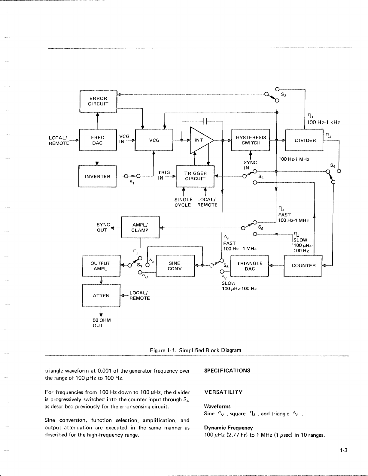
FUNCTIONAL
Programming
Operation
matic
The
coded
range,
selection,
are
to-analog
In
symbols
manded
convertedbythe
whichisappliedtoan
outputsofthese
the
Error
The
CONTROL
the
switches
function,
REMOTE
the
Operations
then
be
REMOTE
trigger,
157
through
for
either
withasynchronizing,
by
data
processing
coding format
program
numerical
and
implementedbyreed-relay
converters
simplified
the
representaswitching
either
voltage-controlled
Loop
Operation
inverter
inputtothe
OPERATIONS
to a
REMOTE
theirRpositions.Control
to
and
each
connector
section.)Anyorallofthese
programmed
connector
and
VCG
separatt
localorremote-program
an automatic
DESCRIPTIONS
contact
(ADP)iscontrolledbybinary
is
modified
controls
amplitude,
generator
(DAC)
block
remotely
frequency
inverter
circuits
generator
remote
closure
mode
diagram of
sourceisaccomplished
pushbuttons
rotary
switch
collectivelyorindependently
in
BCD/binary
on
the
input
signals
BNC
calibration
trigger,orVCG
.
(local/remote) orbyauto-
BCD,BCD,orbinary.The
numerical frequency,
amplitude
selection
contact
.
function
or
locally.The
DAC
and
establish
(VCG)
VCGisdisconnected
and
maybetransferred
formatatthe
rear
panel.Synchro-
are
connectedtothe
connectors
command
range,
.
Circuit
closures
Figure
1-1,
that
binary
into an
error-sensing
the
analog
operating
.
by
turning
of
on the
applications
input
and
can
circuit.The
in
the
generator
controls
rear
simul-
signal
states
frequency
function
functions
cligital-
switch
all
com-
be
code
voltage
state
for
the
search
The
divider
counters
increased.With
is0.001 of
frequency
band
.
.
High-Frequency
Frequences
conventional
outputisa
.
a
square
The
frequency
the
integrator
for
the
square-wave
throughSZtoenable
The
triangle
converter
sinusoidal
S7(triangle,
.
is
the output
by
attenuation
`The
output
uation
network
selected
the
Low-Frequency
Waveforms
are
synthesized
output by the counter
circuit
counts the
0
.001
of
through SZto
frequency
counter
selection
to
the
waveform
consistsofthree
circuit
that
are
progressively
all
three
the
input
rangeofthe
Range
from
100
function-generator
triangle
wave,
specific
which
waveatits
network
with
the
range
output
circuitS,7.All
wave
each
program
and
selects
frequency
output
square,
level
waveform
from
wave
transforms
or
amplifier
.
program
provide
to
Range
frequencies
from
input
input
enable
when
pulseisapplied
DAC
engagedasthe
circuits
frequency
generatortowithin
being
the
is
coupled
output
sine)isthen
over
frequency.One
pulses
that
engaged,
which
Hz
and
establishes
trigger circuit
the
and
pulsestoproduce
1
MHz
to
techniques.The
hysteresis
the
interdependent
the
proper
range
.
the
hysteresis
through S6to
input
the
The
programmed
.
before
then
selects
the
desired
the
100Hzto1MHz
from
100Hzdownto100
basic
waveform
the
trigger circuitinthe
this
mode
throughSstothe
from
the
transforms
cascaded
the
integrating
In
.
given
being
output amplitude
generator
is
the binary
divide-by-ten
frequency
the
divider
reduces
the
error-circuit
are
produced
switch
with
charging
capacitance
the
trigger
switchiscoupled
waveform
function
the
necessary
applied
the
required
square-wave
DAC.The
square
outputisapplied
selected.Another
counter
are
output
the
top
by
integrator
output
the
other
slope
for
mode,
the
sine
into
at
gain
the
to
atten-
for
range
.
jtHz
counter
waves
at
low-
function-
coupled
bits
into
is
is
.
a
a
a
1-2
Page 9
LOCAL/
REMOTE
_
triangle
the
For
is
as
Sine
output
waveformat0
rangeof100
frequencies
progressively
described
previously
conversion,
attenuation
described for the
50
OHM
OUT
.001 of
MHzto100Hz.
from
100Hzdown
switched
for
into
the
function
are
executedinthe
high-frequency
the
generator
to
100
the
counter
error-sensing
selection,
range
amplification,
.
Figure
frequency
pHz,
input
through S
circuit
same
1-1.Simplified
over
the
divider
4
.
and
manner
as
Block
Diagram
SPECIFICATIONS
VERSATILITY
Waveforms
Sine
Dynamic
100
pHz
,
square
Frequency
(2
.77
hr)to1
and
triangle
'v
MHz(1psec)in10
ranges
.
Page 10
Outputs
,
'1,
0
.001 to
3-digit
VCG--Voltage-Controlled
Over
signal
OPERATIONAL
Trigger
Generator
command
cyclesbyapplying
lengthofthe
Input
Plus gate required
10Vp-p
resolution
Output
instrument
1000:1frequency
.
Input
impedanceis10
Mode
may
or
impedanceis10 k
selectable
A,
intoa50-ohm
(0
.002to20Vp-p
may
be
.
MODES
be
triggered
gated
to
a+gate
desired burst
is -+-5
and
NO
TE
shorted
Generator
with
ratio
.
kQ
to
produce
signaltotrigger
.
.
voltsto+50
digitally
loadin4
circuit)
open
without
produce
any
damage
0-voltto5-volt
single
discrete
volts
.
variable
ranges
.
to
cycles
number
input
input
for
from
with
on
the
of
1
digit).Closed-loop
grammed
period
Loop
msec
quency
Manual
Instrument
programmed
ulated
Open-loop
periodatconstant
VCG
1
MHz
Slew
VCG
Frequencyvsinput
±0 .1%
±1%10kHz-100
±3%
frequency
.
will settletowithin the
minimum
and
range
Cal
Mode
can
be
frequency
about
this
stability
Bandwidth
.
rate
100%
of
Linearity
100jHz-10
100 kHz-1
MHz
stabilityiswithin
at
constant
and3sec
.
calibratedtoan
and
accurate
temperature
kHz
center
is
within0.05%
range
per
,usec
voltage--best
kHz
.
.
temperature
accuracy
maximum,
accuracyof-0.02%
triggered
frequency
.
.
straight-line
.005%ofpro-
±0
for
specified
depending on
or
Frequency
.
setting
of
method
24-hour
a
within
for
1
fre-
of
mod-
8-hour
.
Cal
Auto
Generator
ouput
Manual
Generator
is
momentary
triggered
Search
Generator frequency
transferred
control
Sync
Within
quency
1Vp-p
The
Sync
A
impedance
HORIZONTAL
Auto
Frequency
selector
Mode
has an automatic
frequency
Cal
Mode
manually
is
returned
then
switchisreleased
.
Mode
from
for
convenient
In
the upper 4
synchronizedtoan
thatiswithin1%of
induced
fixed
sine
Out
amplitude
for
Cal
Mode
accuracy
Fwitchesis±(0
syncing
PRECISION
for
the
distortion
control
high
accuracy
calibrated
to
the open-loop
control
digital
controls to
manual
ranges,
external
will
square
from
scopes
programmed
.01%
wave
or
of
looptomaintain
and
stability
using
so that
within
sweeping
instrument
the
the
less
be
other
programmed
control
the
condition
may
it
selected
the
a
single
the
of
signalofapproximately
free-running
than1%.
is
brought outat1
equipment
inputorfront-panel
frequency,
.
loop
be
swept
range
turn
entire
may
be
frequency
.
the
but
when
or
analog
range
fre-
plus
is
VERTICAL
Amplitude
kHz
Peak-to-Peak
1Vto10V
0.1Vto1Vrange
10
1mVto10mV
Amplitude
.
All
range
Trigger
amplitude
.
PURITY
Sine
k
Less
Triangle
Greater
PRECISION
change
and0.5
mV
waveforms
Wave
than
0.5%
1%10kHzto100
3%
99%1Hzto100
95%
to
100
Symmetry
.
start-stop
program
'
Distortion
.
100
100
kHzto1
Linearity
than
100
db to
Voltage
range
mV
range
are
MHzto10
:
kHzto1
with frequencyisless
1
MHz
.
Accuracy%of Prograrn
±(0
+5mV)
.1%
±(1%+1mV)
range
±(1%+0
±(1%+0
symmetrical
point
will
.
kHz
kHz
MHz
kHz
MHz
.
.
mV)
.1
.1
mV)
.
about
be 0V±0
than0.1dbto
.
ground
±1%offull
.5%
of
100
output
Page 11
Wave
Square
Less
than
ISOLATION
100
Rise
nsec
and
.
Fall
Time
Configuration
True
Note:-2
False
Note
Logic"1" _
or
volts
or
Logic
Open
:
C
sinks
"0"
circuit
to
-10
--1
volt
volts
.
---2
volts
approximately1.5mA.
= 0
voltage
to
volt
approximately
.
+0.7volts
.
signal
Output
Caution
at
raised
ENVIRONMENTAL
Temperature
Specifications
Operating temperature
REMOTE
ConfigurationA(Standard)
TrueorLogic"1" =0volt
0
Note
:
FalseorLogic
Note:Open
Configuration
TrueorLogic"1"=0
:0volt
Note
FalseorLogic
:
Open
Note
can be
mustbetaken
potential
applyat25°C
CONTROL
volt
sinks
"0"=+2
circuit
B
sinks
"0"=--2
circuit
raised
as
.
range
SPECIFICATIONS
approximately
volts
voltage
volt
approximately
volts
voltage
above
ground up
all
exposed
±5"C
.
0°Cto50°C
±1
volt
.
1.5mA
-
.F
to
10
volts
is
approximately -Q
±1
volt
.
1.5mA
--10
to
approximately-2volts
is
BNC
.
.
volts
connectors
.
.
.
to
volts
250V.
are
.
.
Configuration
TrueorLogic
Note:+2
FalseorLogic
Note:Open
Program
1
MECHANICAL
Weight
24
Power
105
Hz
50
volts
Transition
msec
.
lb,34Ib
Vac
to
.
wattsofpower
Precision
of
selected
D
"'I"
_ +2
sinks
approximately
"0"=0
circuit
voltage
Time
shipping
125
.
Vacor210
required
specifications
range
voltsto+10
volt to +1
approximately-0.7
.
NO
.
volts
1.5mA
volt
Vacto250
TE
over
apply
.
.
.
Vac,50Hz
10%to100%
volts
.
to
400
Page 12

Page 13
SECTION
INSTALLATION
Conversion
The
transformer
otherwise
230-volt
conversion
Board)inthe
should
(Refer to
information
Rack Mounting
The
ordered
when
mounting
adapters,
follows
1.Remove
left
respectively
2.Install
Chassis
supplied
previously
3.Secure
standard
INSPECTION
The
the
user
proper operating
checkout
miningifthe
Visual
After
the
external parts
for
230-Volt
Model
157isshipped
connected
specified.To
operation,
switch
230
be replaced
ReplacementofCircuit
on removing the
Model
157isequipped
for
bench
ordered
:
and
following
Inspection
carefully
for
ofabench
Wavetek
the
right
.
one
rack
Assembly
with
occupied
the
Model
rack
procedures
that
the
instructions
instrumentiswithin
unpacking
Line
Power
from
the
factory
for
115-volt
convert
remove
(locatedonthe undersideofthe
position.The
witha1
use
useina
modelisdesired,
partNo.
flathead
six
side
railstothe
mount
with
the
adapters, using
by the
157inthe
mounting
instrument
condition.Complete
are
for
damage
the
the
bottom
/2-ampere
bottom
with four
and
with
standard
210-367,
machine
adapteroneach
the
flathead
hardware
shouldbeperformed
arrived
has
providedinSection4for
the
instrument,
to
line
transformer
cover
1-ampere
fuse
after
BoardsinSection4for
cover
.)
rubber
rail-attaching
19-inch
two
can
screws
left
and
six
roundhead
the
screws
desired
rack
.
at
its
calibration
electrical
knobs,
dials,
with
the
power
power,
fuse
that
right
tapped
.
position
destination
specifications
visually
unless
primary
and
place
Mother
(rear
panel)
conversion
feet
when
hardware
rack.If
rack
mount
be
used
retain
handles,
sideofthe
screws
holes
with
to assure
deter-
inspect
indicators,
rack
and
for
the
the
in
as
surface
the
Operating
The
.
checkoutofinstrument
exist,
following
for
and
y1. .
10.Depress
.
11.Depress
12.Step
areas,
carrier
RefertoInstallation
230-volt
procedural
refertothe
performing
Figure
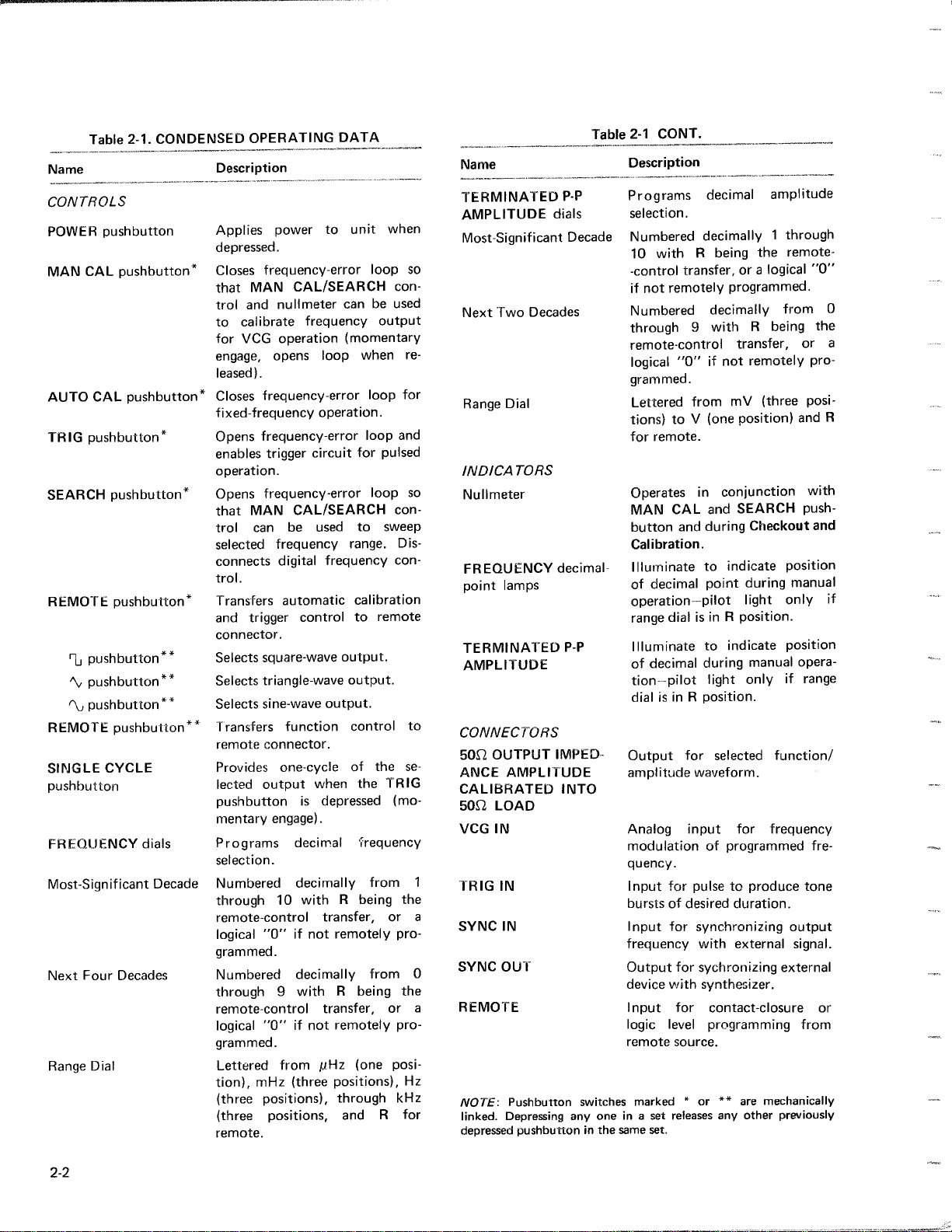
Name
Oscilloscope
Depress
2.Connect
50Q
3.Depress
4.Depress
5.Set
FREQUENCY
6.Set
TERMINATED
V
.
7.Observe
correctnessofthe
8.Depress
outputis+5
9.Press
put
shouldgoto
to+5Vdc
CAUSEARCH
clockwisetomaximum
should respondtofrequency
100
Hz
indicated
from
100Hzincrements
TI
etc.If
damageisdiscovered,
who
transported
Inspection
line
power
stepsinthis
Warrantyinthe
test
equipment,orequivalent,isrecommended
the
electrical
2-1
for operating
POWER
OUTPUT
AUTOCAL
oscilloscope
the
SINGLE
the
to
the
and ",,in
waveform
the
10 through1.
pushbutton
oscilloscope
connector
pushbutton
'
-
L
signal
TRIG
Vdc
.
CYCLE
---5
each
time the
SEARCH
control
more
than
AUTO
most-significant-decade
INSTRUCTIONS
the
instrument
NOTE
paragraph
instructions
paragraph
operation.If
frontofthe
inspection.(RefertoTable
control
Manufacturer
Tektronix
_m.._
.
through
.
pushbutton
.
dials
for
1000
P-P
AMPLITUDE
displaytodetermine
output
pushbutton
pushbutton
Vdc
for0.5
pushbuttonispressed
pushbutton and
from
clockwise
1
kHz
over
CAL
pushbutton.Depress
.
Output
turn
.
Output
from1kHzto100Hz.
should
.
for
115-volt or
.
electrical
descriptions
50-ohm
.
.00Hz.
for
Steps
and
observe
several
milliseconds
maximum
positions.Output
control
the
control
should
FREQUENCY
change
fileaclaim
provideaquick
manual.The
terminator
dials
8 through 16
rotate
from
respond
frequency
with
deficiencies
2-1
.)
Model
454
to
for10.00
the
general
that
the
times.Out-
and back
.
MAN
the
counter-
less
than
range
.
the
with
dial
in
.
Page 14
2-1
CONT
Table
2-1
Name
CONTROLS
POWER
MAN
AUTO
TRIG
SEARCH
REMOTE
REMOTE
SINGLE
pushbutton
pushbutton
CAL
CAL
pushbutton*
pushbutton*
pushbutton*
pushbutton
'1,
'",,
pushbutton**
r\,
pushbutton
pushbutton
CYCLE
pushbutton
pushbutton
FIR
FOUFNCY
dials
Most-Significant
Next
Four
Decades
Dial
Range
CONDENSED
.
**
**
**
Decade
OPERATING
Description
Applies
depressed
*
Closes frequency-error
that
trol
to
for
engage,
leased)
*
Closes
power
.
CAL/SEARCH
MAN
nullmeter
and
calibrate
VCG
frequency
operation
opens
.
frequency-error
fixed-frequency
frequency-error
Opens
enables
operation
Opens
that
trol
selected
connects
trol
-
I"ransfers
and
connector
Selects
Selects
Selects
Transfers
trigger circuit
.
frequency-error
MAN
CAL/SEARCH
can
be
frequency
digital
.
automatic
trigger
control
.
square-wave
triangle-wave
sine-wave
function
remote connector
Provides
lected
pushbutton
mentary
Programs
selection
Numbered
through 10
one-cycle
output
is
engage)
decimal
.
decimally
with
remote-control
logical
"0"ifnot
grammed
Numbered
through 9
.
decimally
with
remote-control
logical
"0"ifnot
grammed
Lettered
tion),
mHz
.
from
(three
(three positions),
(three
remote
positions,
.
DATA
unit
to
when
loop
can be
output
(momentary
when
loop
loop
operation
.
loop
for
pulsed
loop
to
range
sweep
.
used
frequency
calibration
remote
to
output
.
output
.
output
.
control
.
of
the
when
the
TRIG
depressed
(mo-
.
Frequency
from
R
being
transfer,
or
remotely
from
R
being
transfer,ora
remotely
PHz
(one
posi-
positions),
through
and
R
so
conused
re-
for
and
so
con-
Dis-
con-
to
se-
the
pro-
the
pro-
Hz
kHz
for
Table
Name
TERMINATED
AMPLITUDE
dials
Most-Significant
P-P
Decade
Description
Programs
selection
Numbered
10
-control
if
not
Next
Two
Decades
Numbered
through
remote-control
logical
grammed
Range
Dial
Lettered
tions)
for
INDICATORS
Nullmeter
Operates
MAN
button
Calibration
FREQUENCY
lamps
point
clecimal-
Illuminate
decimal
of
operation--pilot
range
TERMINATED
AMPLITUDE
P-P
Illuminate
of
decimal
tion--pilot
dialisinRposition
CONNECTORS
OUTPUT
502
ANCE
AMPLITUDE
CALIBRATED
5052
LOAD
VCG
IN
IMPED-
INTO
Output
amplitude
Analog
modulationofprogrammed
quency
1
TRIG
IN
Input
burstsofdesired
a
SYNC
IN
Input
frequency
SYNC
0
OUT
REMOTE
Output
device
Input
logic
remote
:
NOTE
Pushbutton
linked.Depressing
depressed
pushbuttoninthe
switches
any oneina
same
marked*or**are
set
set
.
decimal
.
decimally
with
R
transfer,
remotely
9
"0"ifnot
.
from
V
to
.
remote
in
CAL
during
and
.
to
point
dialisin
to
during
for
waveform
input
.
for
pulsetoproduce
for
synchronizing
with
for
sychronizing
with
synthesizer
for
level
source
releases
.
amplitude
1
through
the
a
logical
remote-
being
or
programmed
decimally
with
R
from
being
transfer,
remotely
mV
(three
(one
position)
and
conjunction
and
SEARCH
Checkout
during
light
position
manual
only
position
manual
only
.
position
opera-
if
indicate
R
indicate
light
.
selected
function/
.
for
frequency
duration
.
output
external
signal
external
.
contact-closure
programming
.
mechanically
any
other
previously
"0"
.
the
or
pro-
posi-
with
push-
and
range
fre-
tone
or
from
0
a
R
if
.
2-2
Page 15
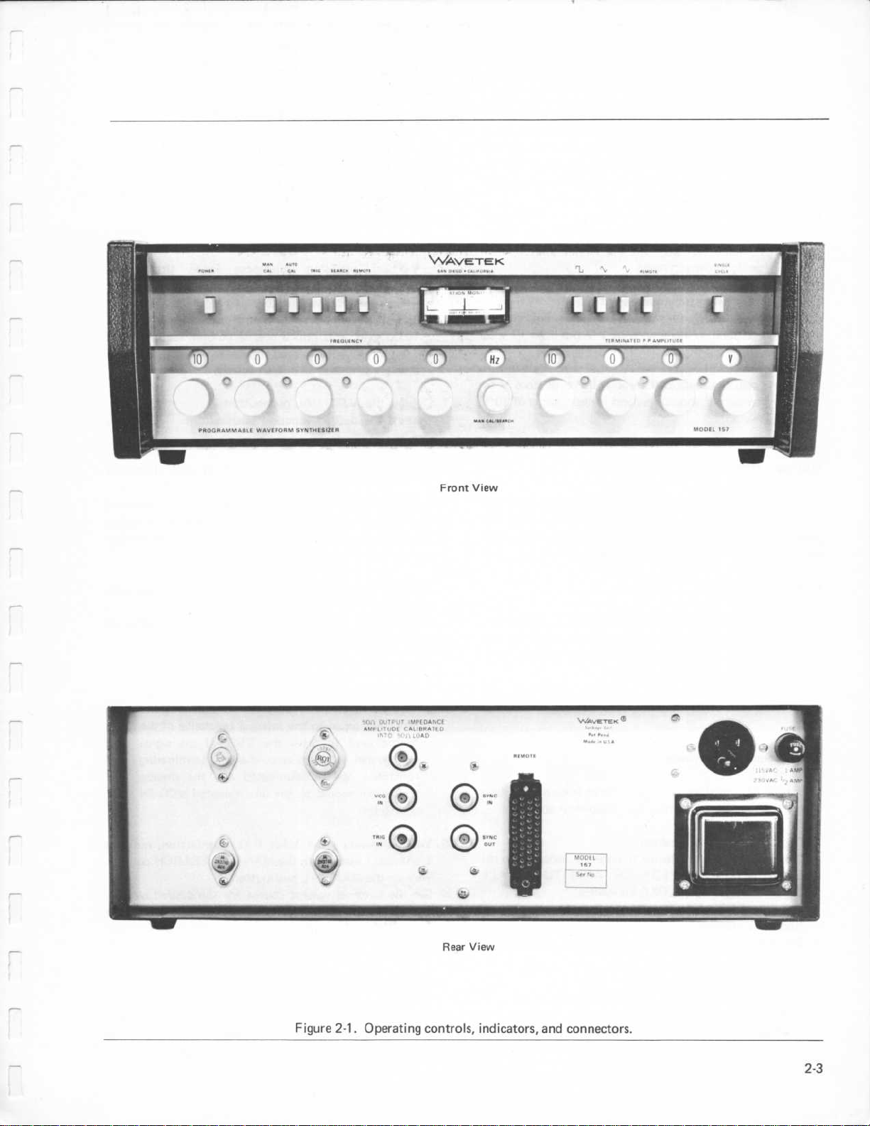
2-1.Operating
View
controls,
View
indicators,
and
connectors
Front
Figure
Rear
.
2-3
Page 16
INTRODUCTION
This
section
user
Programmable
Section5graphically
the
Model
theoretical
references
schematic
used
complicated
six
discussional
1.Programming
2.The
3.The
4.Sine
5.Tone-burst
6.Power-supply
presents
in
understanding
Waveform
157 and
discussion.In
are
diagramsinSection5and
in
this
100
Hz
100
pHzto100Hzgeneration
conversion
should
made
sectiontosupplement
circuits.The
parts
the
various
1
MHz
to
.
generation
characteristics
theoryofoperationasan
and
maintaining
Synthesizer.The
illustrates
throi--ighout
theoryinSection3is
:
generation
.
the
functional
be referenced
addition to
the
text to
simplified
generator
characteristics
.
.
.
when
the
the
the
block
block
specific
diagrams
text
divided
aidtothe
Model
diagram
features
reading
diagram,
board
for
more
.
157
in
of
the
are
into
MAN
CAI_
switching
across
the
error
VCG
first
may
cll3
:,trc-i
SEARCH
inverter
the
disconnected
enables
singie
SEARCH
TRIG
Board
ofK6closes,
the generator
(Refer
additional
amplifier
be
accurately
priortoanAqg
switching
output and^the
first
VCG
the
frequency
control
switching
which
the
to
details
cul
(momentary)
amplifier
amplifier.Also,
from
VCG
to
range
.
turnsondriverQ8on the VCG/Integrator
energizes
causing
subsequently
descriptionoftone-burst generation
.)
input
set
control
connects
rnanual
the
first
swewp
%vith
relayK6.
emitter
output and
so that
with
the
operation
the
calibration/search
the
VCG
the
one
The
followerQ9to turn
enters
CRIPTI
connects
output
the
the generator
MART
CAL/SEARCH
.
nullmeter
error
amplifier
amplifier
generator
basic
turn of
the
normally-open
the standby
the
frequency
between
input,
MAN
condition
nullmeter
into
the
the
input
to
output
which
over
any
CAL/
contact
off,
and
for
is
.
PROGRAM
Generator
The
generator-mode
the
block
Assembly
Board
the generator
functions occur
REMOTE
voltage inputtothe
controloferror
connector
canbeprogrammed
AUTO
voltage
error
generator
SELECTION
Mode
Selection
diagram
schematic
schematic
switching
pin
CAL
input
amplifier
operatesinclosed-loop
and
diagram.When
mode
.
amplifier
so that
.
switching
to the
outputtothis
selection
diagram
rowisdepressed,
either
first
circuitisgraphically
detailedonsheet1of
and
also
one
of the pushbuttons
disables
first
disconnects
the
MAN
VCG
amplifier
output
closed-looporopen-loop
VCG
relayK5toaremote
the
amplifier
amplifier
.
shown
the
Chassis
the VCG/Integrator
the
MAN
and
so that
following
CAL/SEARCH
CAL/SEARCH
and
transfers
connects
the
circuit
mode
basic
the
in
in
Function
The
the
Assembly
schematic
is
depressed,
REMOTE
pushbuttons
nectortothe
Function
`Lswitching
to
Board
^
vswitching
to
Board
ti
to
Board
Selection
function-mode
block
diagram
diagram.Whenaspecific
switching
Board
provide
.
provide
.
switching
provide
.
selection
and
schematic
the following
disconnects
and
connects
sine,
square,
.
energizes
the square
energizes
the
triangle
energizes
the
sine
circuitisgraphically
detailedonsheet1of
diagram
waveform
waveformtothe
waveform
and
the
pushbutton
circuit
functions
the
front-panel
the
pins
on the
and
triangle
relay
K3 on
relay
K2 on
relayK1on the Function Board
to
to
relay
the
the
the
the
the
Function
occur
remote
driversonthe
Function
Output
Function
Output
Output
shown
Chassis
Board
this
row
in
:
function
con-
Board
Amplifier
Board
Amplifier
Amplifier
in
Page 17
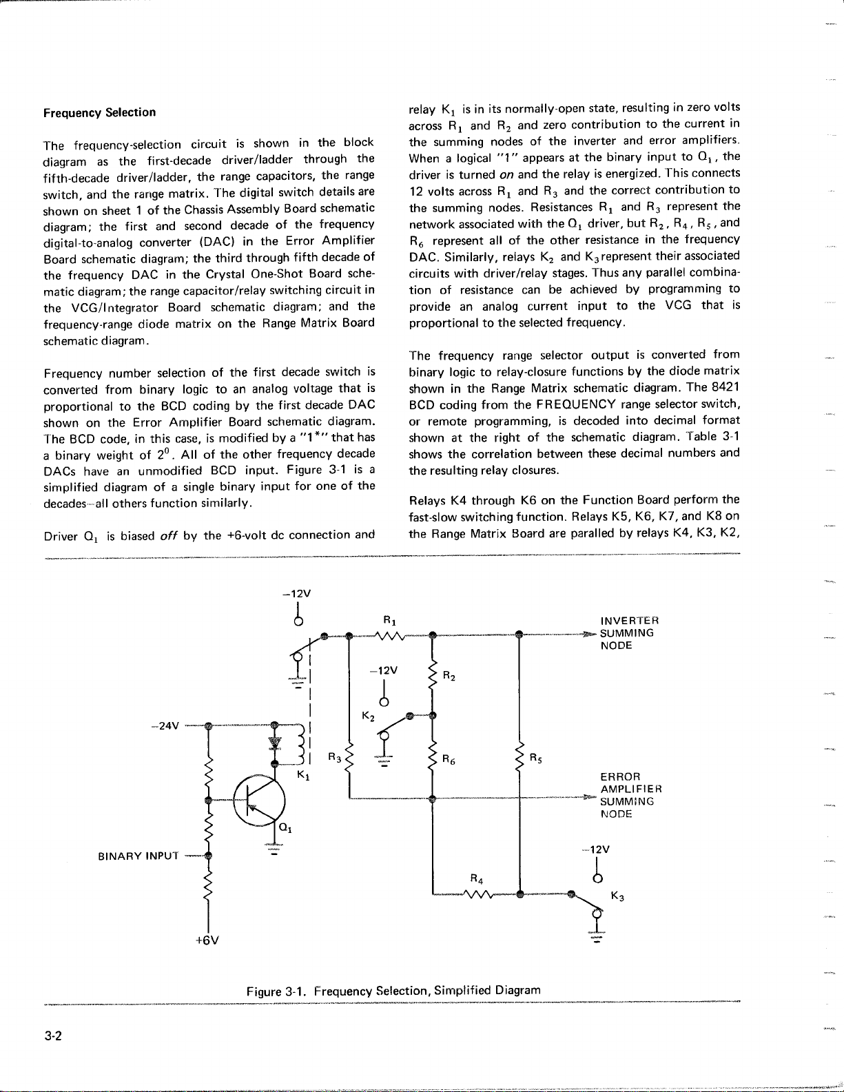
Frequency
The
diagram
fifth-decade
switch,
shown
diagram;the
digital-to-analog
Board
the
Selection
frequency-selection
as
the
driver/ladder,
and
the
range
on
sheet1of
first
converter
schematic
frequency
diagram;the
DAC
matic diagram;the
the
VCG/Integrator
diagram
number
from
diode
binary
frequency-range
schematic
Frequency
converted
proportionaltothe
shown
The
a
simplified
decades..
on
the
BCD
code,
binary
weightof2°.
DACs
have an unmodified
diagramofa
-all
Error
in
others
Driver01isbiased
circuitisshown
first-decade
driver/ladder
the
range
matrix.The
the
Chassis
Assembly
and second decade
(DAC)
third
in
the
Crystal
range
capacitor/relay
Board
schematic
matrixonthe
.
of
selection
logic
BCD
Amplifier
this
case,ismodifiedbya
the
to an
coding by the
Board schematic diagram
Allofthe
BCD
single
binary
function
off by
similarly
the
+6-voltdoconnection
in
capacitors,
digital
switch
Board
of the frequency
in
the
Error
through
fifth
One-Shot
switching
diagram;and
Matrix
Range
first
decade
analog
voltage
first
"1
frequency decade
other
input.Figure
for
input
.
the
block
through the
the
range
details
are
schematic
Amplifier
of
decade
Board
sche-
circuit
the
Board
switch
that
*"
that
3-1
DAC
has
is
decade
oneofthe
and
in
is
is
K1isinits
relay
across
the
summing
Whenalogical
driveristurnedonand
12
volts
the
summing
network
R6represent
DAC.Similarly,
circuits
tionofresistance
provide
proportionaltothe
'The
frequency
binary
showninthe
BCD
coding
.
or
remote
shown
shows
the
a
the
resulting
RelaysK4through
fast-slow
the
Range
normally-open
R1andRz
acrossR1
associated
with
and
zero
nodes
"1"
nodes
all
relays
the
of
appears
the
R3and
and
ResistancesR1
.
with
the01
the
other
of
KZandK3
relayisenergized.This
driver/relay stages.Thus
can be
an
analog
current
selected
range
selector
logictorelay-closure
Range
Matrix
from
programming,
at
the
correlation
relay
switching
Matrix
right
FREQUENCY
the
is
of
the
between
closures
K6 on
.
the
function.Relays
Board
are
state,
resultinginzero
contributiontothe
inverter
at
and
error
the
binary
input
the
correct contribution
andR3
driver,
butR2,R4,
resistanceinthe
represent
achieved
input
frequency
output
functions
schematic
decoded
schematic
these
Function
their
any
parallel
programming
by
to
the
.
is
converted
by
the
diagram.The
range
selector
into
decimal
diagram.Table
decimal
Board
K5, K6,
paralled
by
relays
current
amplifiers
to
Q1,
connects
represent
R5,
frequency
associated
combina-
VCG
diode
numbers
perform
K7,
andK8on
K4, K3, K2,
volts
in
the
to
the
and
to
that
is
from
matrix
8421
switch,
format
3-1
and
the
.
3-2
BINARY
-24V
INPUT
Figure
3-1.Frequency
Selection,
Simplified
Diagram
Page 18
Table
3-1.FREQUENCY
RANGE
CODING
Table
3-2.ATTENUATOR
RANGE
CODING
Board
Desig
A11
A11
A11
A11
A11
A11
A11
A11
A10
A10
A10
A10
A9
and
switch
range.(Refertodescription
tional
provide
connect
frequency
(Josed-loop
generator for
The
the
proper
shown
diagram
Amplitude
The
diagramasthe
The
Chassis
the amplitude
schematic
on
sheet2of
The
frequency-number
The
Output
anda40-db
switched
binary
code
Relay
Desig
K1
K2
K3
K4
K5
K6
K7
K8
K4
K3
K2
K1 0 0
K4-6 0
K1
on the VCG/Integrator
the
in
details.)The
circuit
to
the
generator.(Refertothe
additional
frequency
decimal-place
on
sheet1of
.
Selection
amplitude-selection
digital
amplitude-number
amplitude-range
expandedtolist
switch
Assembly
diagram;and
the
Attenuator
into
program.Table
1
0
0 0
0
1
0 0
0 0
0 0
1
0 0
0 0
correct
relays
switching for the
crystal
basic
generator
range
selector
signal
attenuator
details
schematic
attenuationonthe
Chassis
DAC
selection
Board,
attenuator,
the
pathofthe output
associated
0 0 0 0 0 0 0 0
1
0 0
1 1
1 1
0 0 0
capacitance
on the
one-shot
details
indication
the
circuitisshown
the range/attenuation
Assembly
selection circuitryissimilartothe
circuit
3-2isa
Digital
.-.. .
0 0
1
0 0
0 0
0 0
0 0
0 0
0 0
of
.)
(SW6)
Chassis
are
shown
diagram;the
previously
circuit,
consistsofa 20-db
eitherorboth
circuit
Program
.3
.-4
._-5
0
0 0
0 0
1
1
1
Board,
and
and
truth
0 0
1 1
0
0
1
0 0
0
1
0 0
0
0
0
1
0
0
1
0 0
0 0
respectively,
for
the
basic
generator
Range
Matrix
divider
circuit
Output
andtothe
descriptions of
the
also
applies
lamp
(L1,
Assembly
the
range
on
sheet1of the
three
Amplifier
schematic
described
contained
waveform
tableofthe binary
functions
0
0
0
0
0
flip-flops
low-frequency
diagram
of
67
0
0
0
1
0
1
0
0
1
0
1
0
0 0
1 1
programmed
for
Board
power
L2,orL3)
schematic
in
the
attenuator
decades of
circuit
.
on the
attenuator
which
by
.
.8_
. .._.
0
0
0 0
0 0
0 0
1
0
0 0
0
1
1
which
addi-
also
that
low-
the
block
Board
(A5)
.
are
the
to
as
9
0
0
0
0
1
0
0
1
1
A5-6 A5-7
0
1
0
1 1
NOTE:X
------
BASIC
The
and
integrator,
duces both
MHz
1
operation,
frequency-converter
connected
the
input
Open-Loop
When
integrator
thatisequaltooneofthe threshold
switch.The
regeneration
If
the
the diode
integrator(DZinFigure
connecting
switch(D3).
the
frequency
nodetothe
.
the
output
reverses
diodeD3topermit
amplifier
precisely
first
equalinvalue,
produced by the
I"he
negative
integrator
again
The
equal
0
0
1
denotes
-----------
GENERATOR
basic
generatorisshowninblock
second
and
triangle
range
the
between
of
power
causes
bistable
connecting
triangleisformedatthe
level
statetoprovideapositive
into
twice
VCG
amplifier
net
current
slopeofthe
output
reverses
output
in
value,
attenuatorincircuit
voltage-controlled
hysteresis
the
and
in
open-loop
divide-by-ten
circuit,
the
first
the
Operation
switch
proceedsinthe following
the
first
voltagesofthe
VCG
applied,
is
this
devicetoproduce
assumes
output of the
second
this
With
program
VCG
reaches+2.5
currenttoflow
the
integrator
the
valueofthe
;
therefore,
butinthe
negative
causes
reaches
states
and
but
oppositeinpolarity,
Range
(max) 20-db 40-db
10
mV
100
mV
1000
mV
10V
generator
switch.This
square
waveforms
operation.For
stages,
and
outputofthe
.
high-gain
the
one
hysteresis
the second
3-2)iszero biasedbythe
VCG
amplifiertothe
condition,
flows
from
amplifier
opposite
triangleatits
---2
the
and
integrator
volts,
summing
current
a
outputofthe
the
integrator
.5 volts,
cycleisrepeated
two
VCG
X X
X
.
diagramasthe
amplifiers,
generator
over
the
one-shot
the
error
hysteresis
characteristicofthe
an output
levels
of the
of
its
binary
manner
switch
VCG
amplifier
current
the
output.This
net
direction,
proportional
integrator
the
positive
output.When
the
hysteresis
from
the
node.This
flowing
current
hysteresis
to produce
output.When
the
hysteresis
.
amplifiers
a
100Hzto
closed-loop
stage,
amplifier
switch
voltage
hysteresis
states
.
negative,
is
to
hysteresis
summing
slope
switch
zero
second
current
into
flows
that
the
current
to
switch
switch
are
always
and
directly
X
first
the
pro-
the
are
and
and
the
diode
to
of
the
biases
VCG
is
the
is
.
the
the
3-3
Page 19
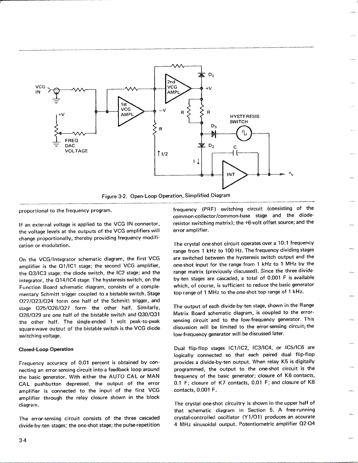
Figure
3-2
.
Open-Loop
Operation,
Simplified
Diagram
the
proportional
Ifanexternal
voltage
the
change
cation or
On
the VCG/Integrator
levelsatthe
proportionally,
modulation
amplifieristhe
the
Q3/IC3
integrator,
Function
mentary
022/Q23/Q24
stage
028/029
the
the
Board
Schmitt
Q25/Q26/Q27
are
other
square-wave
switching
voltage
Closed-Loop
Frequency
accuracyof0
frequency
to
voltageisappliedtothe
thereby
.
Q1/IC1
the
;
Q14/IC4
diode
stage
schematic
trigger
form
one
form
one
halfofthe
.
The
half
outputofthe
.
Operation
nectinganerror-sensing
the
basic
generator.With
CAL
pushbutton
depressed,
amplifierisconnected
amplifier
diagram
The
divide-by-ten
through
.
error-sensing
stages;the
the
circuit
program
.
VCG
the
outputs
providing
schematic
stage;the
switch,
stage.The
diagram,
coupledtoa
halfofthe
the
bistable
VCG
of
diagram,
second
the
hysteresis
consists
bistable
Schmitt
other
switch
frequency
IC2
half.Similarly,
single-ended1volt
bistable
.01
circuit
either
to
relay
switchisthe
percentisobtainedbycon-
a
feedback
into
AUTO
the
the
output
the
inputofthe
closure
shown
consistsofthe
the
one-shot
stage
pulse-repetition
;
IN
connector,
amplifiers
modifi-
first
the
VCG
VCG
amplifier,
stage;and
switch,onthe
a
comple-
of
switch.Stage
trigger,
and
Q30/Q31
peak-to-peak
VCG
diode
loop
around
CAL
or
MAN
of
the
error
first
VCG
in
the
block
three
cascaded
will
the
and
frequency
(PRF)
switching
common-collector/common-base
.
one-shot
between
for
(previously
are
course,
1
MHztothe
schematic
and
will
be
generator
stages
the output
matrix);the
circuit
Hz.The
hysteresis
the
range
the
discussed).Since
cascaded,atotal
is
sufficienttoreduce
one-shot
divide-by-ten
diagram,iscoupled
to
the
limited
to the
willbediscussed
IC1/IC2, IC3/IC4,
that
so
output.When
to
basic
generator;closure
contacts,
resistor
error
The
range
are
one-shot
range
switching
amplifier
crystal
from1kHzto100
switched
input
matrix
by-ten
stages
which, of
top
range
of
outputofeach
The
Matrix
sensing
Board
circuit
discussion
low-frequency
Dual
flip-flop
logically
connected
providesadivide-by-ten
programmed,
frequencyofthe
F;closureofK7
0
.1
contacts,0.001F.
crystal
schematic
one-shot
The
that
crystal-controlled
4
MHz
sinusoidal
circuitryisshown
diagram
in
oscillator
output
Potentiometric
.
circuit
(consisting
stage
+6-volt
operates
offset
overa10
frequency
switch
from1kHz
0
of
the
rangeof1
top
stage,
shown
low-frequency
error-sensing
each
paired
relayK5is
the
one-shot
0
.01F;
in
Section
(Y1/01)
5.A
producesanaccurate
the
and
source;and
frequency
:1
dividing
output
1
MHz
to
the
three
.001Fis
basic
available
generator
kHz
the
in
the
to
generator.This
circuit
later
.
IC5/IC6
or
dual
circuit
of
K6
contacts,
and
closureofK8
the
upper
free-running
amplifier
the
of
diode-
the
stages
and
the
by
the
divide-
.
Range
error-
;the
are
flip-flop
digitally
is
the
half
of
Q2-Q4
3-4
Page 20
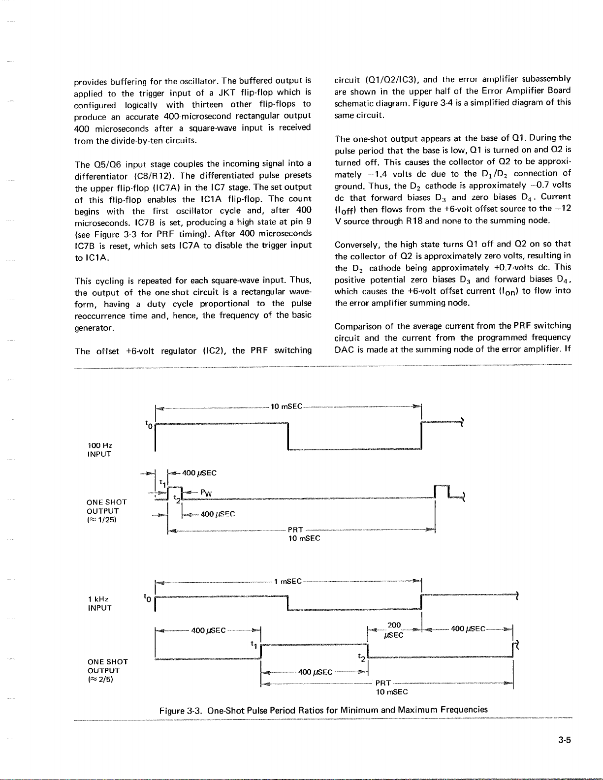
provides
buffering
appliedtothe
configured
produce
400
microseconds
from
The
Q5/06
logically
an
accurate
the
divide-by-ten
input
differentiator
this
flip-flop
flip-flop
with
the upper
of
begins
microseconds
(see
Figure
3-3 for
IC7Bisreset,
to
IC1A
.
cyclingisrepeated
This
the output
form,
of
havingaduty
reoccurrence
generator
The
.
offset
+6-volt
for
the
trigger
inputofa
with
400-microsecond
afterasquare-wave
circuits
stage
couples
(C8/R12).The
(IC7A)
enables
first
PRF
sets
oscillator
timing)
the
.
IC7Bisset,
which
for
the
one-shot
cycle
and,
hence, the
time
regulator
oscillator.The
JKT
thirteen
other
rectangular
.
the incoming
differentiated
in
the
the IC7
IC1A
stage.The
flip-flop.The
cycle
a
After
.
high
producing
IC7Atodisable
each
square-wave
is
a
circuit
proportionaltothe
frequencyofthe
(IC2),
the
buffered
output
flip-flop
flip-flops
input
is
signal
pulse
set
after
and,
stateatpin
400
microseconds
the
trigger
input
rectangular
PRF
switching
which
output
received
into
presets
output
count
400
input
.
Thus,
wave-
pulse
basic
to
is
circuit
is
are
shown
schematic
same
circuit
The
one-shot
pulse
turned
a
mately
ground.Thus, theDz
do
that
(loff)
9
V
source
Conversely,
collectorofQ2isapproximately
the
theDZ
positive
which
the
error amplifier
Comparison
circuit
DACismadeatthe
(01/02/IC3),
in
the
upper
diagram.Figure 3-4
.
output
period
that
the
off.This
causes
---1.4voltsdodue
forward
then
flows
biasesD3
from
throughR18
high
the
cathode
potential
causes the
being
zero
+6-volt
summing
the
average current
of
and
the
current
summing
and
error amplifier
the
halfofthe
a
simplified
is
appearsatthe
baseislow,
the
cathode
Q1isturned
collectorofQ2tobe
the
to
approximately
is
and
the
+6-volt
and
nonetothe
state
turnsQ1off
Error
baseofQ1.During the
D1/D2
zero
offset
summing
zero
subassembly
Amplifier
diagramofthis
on and02is
connection
biasesD4.Current
sourcetothe
andQ2on
volts,
approximately+0.7-voltsdc.
biasesD3
offset
from
node
node
and forward
current
.
from
the
programmed
of the
(Ion)
the
error
to flow
PRF
Board
approxi-
of
--0.7volts
-12
node
.
so that
resulting
in
This
biasesD4
into
switching
frequency
amplifier.If
,
100Hz
INPUT
ONE
OUTPUT
(^
1/25)
1
kHz
INPUT
ONE
OUTPUT
(-2/5)
SHOT
SHOT
Figure
3-3.One-Shot
Pulse
Period
10
mSEC
Ratios
for
Minimum
and
Maximum
Frequencies
3-5
Page 21
FROM
FREQUENCY
DAC
1-O
ERROR
AMPLIFIER
SUMMINGNODE
the
magnitudes and
equal
and
opposite,
to
cause
The
ac anddc.
capacitor
fier
the
to
schematic
shown
two-pole
error
provide
The
causes
modifies
direction
the
equalinamplitude
current
this
frequency
programmedinspiteofcomponent
error-voltage
an
error amplifier
Since
provides
C8
saturation.The
MAN
diagram)
on
the
filter
pathtofurther
signal
proper
error
signal
a changeinthe
the output
(either
error
currentatthe
from
the
manner,
of
polaritiesofthese
an
error
current
output
has
considerable
the
PRF
current
negative
outputofthe
CAL
switch
and
latter
(R5,
loop
damping
thatisappliedtothe
frequency
and
digitally-programmed
the
error-sensing
the
basic
(sheet
the VCG/Integrator
to
schematic
R6, R7, C28,
reduce
.
VCG
output
frequency
increaseordecrease)tocause
error
amplifier
opposite
generator
Figure
3-4.PRF
currents
will
result
at
from
the
forward
largeaccomponent,
has
a
feedback
error
1ofChassis
diagram,
C25)isinsertedinthe
ripple
the
VCG
voltage
the
basic
of
summing
polaritytothe
in
circuit
to
value
amplifier
error
gain
to
prevent
amplifier
an
voltage
summing
that,inturn,
generatorinthe
frequency
holds
the output
the
value
drifts
.
Switching
are
not
the
node
.
for
both
ampli-
applied
is
Assembly
Board.As
additional
and
to
node
node
to be
analog
DAC.In
that
Circuit,
LOW-FREQUENCY
Triangle
frequency
Hz.'This
counter,
Slow
The
to
506 and
square-wave
frequency
states
basic
the
may
range
same
frequency
The
Section5.
not
other
which
is
output.Whenatrue
Simplified
and
circuitry
and
Square-Wave
cyclic
are
generator
low-frequency
be
of
as
simplified
shown,
inputstothe
require
Diagram
square
ranges
triangle
counter
then
outputs
from
progressively
and
extended
the
instrument.This
previously
inputtothe
logic
The
parallel
but
all
GENERATOR
waveforms
covering
consists
Generation
the
enter
of
DAC
showninthe
is
logically
back
that
basic
switched
the
inputtothe
range
(100
down
described for
error-sensing
diagram
trigger
directly
flip-flops
inputs to
output
are
the
band from
the
divide-by-ten
configured
down
are0.001
generator
between
Hz)ofthe
to
the
operation
for
inputs to
without
are
be
from
digitally
100
block
to count
againtoproduce
to
6
F
The
.
the outputofthe
cyclic
MHz
100
is
providing the
circuit
.
counter
the
each
being
controlled
false
to
NOR
a
gate
in
generated
pHz
stages,
diagram
of
divide-by-ten
countersothat
basic
low-frequency
essentially
flip-flop
by
produceatrue
occurs,
the
to
100
cyclic
.
from
the
input
generator
the
correct
appears
gated.All
NOR
gates
both
are
6
in
3-6
Page 22
the
set
and
change
terminal
When
clock-pulse
pulse inputtobegin
starting
the
the
Two
counter
boards
on
tone-burst
to
As
slow
provides
Q5/06
drivingacompound
supply
output.Stages
equivalent of
negative-excursionofthe
Slow
state
.
the
with
counter
is
cycle
binary
as
The
.
the
VCG/Integrator
the
square-wave
shown
I
the
and
for
Triangle
last
generator
inputs
reset
with
the
flip-flopinthe
input,
the
the
highest
output
repeated
(square-wave)
square
No
in
is
5-volt
the
steps
.
waveforms and
256
.
theory),
amplifier/clamponthe Function Board
the Function
appliedtothe
peak-to-peak
Q9/Q10
configurationtoprovide
positive
Q7/Q8
the
circuitry
Wave
Generation
are
enabled
next
clock pulse
counterissetattheNo.
logic
gating
sequentially
flip-flop
order
down
outputs
count
and
coupledtothe
is
Board
and
Board
amplifier/clamp
consistofa
excursion
Q11/Q12
just
square-wave
and
into
causes
resetting
.
Thus
until
No
.
are
taken
connected
(described
theNo.
square-wave
described
506
schematic
differential
of
the
are
the
output
the
flip-flop
its
trigger
input
the
next
clock-
flip-flops,
the
afterNo.
6isreached
from
trigger
output.Stages
complementary
and
.
cyclic
the
to
other
circuit
laterinthe
countissent
diagram,
circuit
amplifier
the
collector
square-wave
provide
will
506
506,
and
the
that
the
SINE
CONVERSION
The
selected,
intoasine
block
diagram
this
circuitry
network
(IC2/Q1-04).Figure 3-6
The
forms
the top
adjust
Conversionofthe
accomplished by
.
resistor
the diode
simplified
parallel-connected
of
wave
waveisobtained
Duetothe
amplitudeofthe
before
IC2/Q1-Q4
the
(IC3
triangle
the
and bottom
the
networks
both
positive
so that
applicationtothe
required
sloworfast,
waveform
.Inthe
is
shownasa
through
inputisappliedtoclipper
triangle intoatrapezoidal
positive
curve.Only
diagram
and
four
which
and
and
shape and amplitude
.
losses
inherentinthe
shaped
formapotentiometric
gain
.
triangle
by
the
Function
IC6),
simplifies
peaks.Potentiometers
negative
trapezoidal
temperature-compensated,
are
one
of
Figure 3-6;the
biased
negative
sine
Output
waveformistransformed
sine
Board
clipper
andapotentiometric
this
amplitudes
wave
biased to
such
networkisshowninthe
operateatdifferent
to
excursionsofthe
sine-shaping
wave
Amplifier
convertor
(IC1),
waveform
into
operateatthe knee
symmetry
requires
amplifier
showninthe
schematic
diode-shaping
the
circuitry
IC1
which
R6
.
the
sine
other three
process,
amplification
Board.Stages
that
amplifier
for
by
and
trapezoidal
of
diagram,
clarity
trans-
clipping
R15
wave
diode-
of
are
levels
the
sine
the
provides
.
is
The
triangle
digital-to-analog
slow
frequency
"The
switching
tor
(IC22),
amplifier
schematic diagram.The
binary
configuratedtoprovideacountof500
Figure
binary
to
switchonin
these bridges
from
the
Fofthe
'The
slow
switching
(discussed
circuits
DAC,
triangle
ranges of
triangle
circuits
the
(IC24/Q3/Q4)
outputs
3-5isa
inputs
from
are
summing
basic
generator
triangle
circuit
later)
(discussed
showninthe
converter,
waveform
the
instrument
DAC
consistsofthe
(IC25 through
---6-volt
simplified
their
and
regulator
counter
up
to29
diagramofthe
the
counter
logical
connectedinparallel,
amplifierisa
frequency
outputisconnectedtothe
for
application
the
function-selection
previously)
block diagramasthe
produces
over
the
IC33), the
(IC23),
shown
on the
and
(51210),
cause
binary
triangle
.
.
the
digitally-generated
pHz
100
.
nine
diode-bridge
+6-volt
and
the
Counter
DAC
are
but
are
.
triangle
the
nine
diode-bridges
sequence.Since
the
resulting
waveformat0
slow/fast
to the
sine
relay-switching
100
to
regula-
summing
Board
capable
logically
DAC.The
all
output
relay
converter
9-bit
Hz
of
of
.001
TONE
BURST
When
the
programmed
VCG/Integrator
relay
K6,
close
(Figure
Priortothe
is
turned
associated
statebyapproximately+3voltsatthe
stateofIC6
provides
Turn
offofQ9,
the
flip-flop,
the
flip-floptoassume
is
nowapositive
base
amplifier
011.The
short
circuit
through
"standby
GENERATION
TRIG
pushbuttonisdepressed,ora
during
causing
3-7)
closingoftheK6contact,
on
resistors,
disables
its
programmed
and
feedback
the
Q13/Q11
state"---no
remote
Board draws
the
normally-open
.
by
the
and
the standby
however,
the
voltage
Q12
which,inturn,
path
around
output
operation,
+12-volt
flip-flop
output
removes
next
square-wave clock
the
reset state.The
sufficienttoturnongrounded-
around
the
programmed
path
and
.
current
path
IC6isclampedinthe
circuit
.
the
enables emitter
the
the
logical
driverQSon the
through
contactofthis
emitter
through
preset
set
integratorisnow
integratorisin
and
state
set
range
the
follower
input.The
the
integrator
clamp
input
output,
capacitance
"1"
coil
relay
CR5
from
causes
"Q",
follower
is
of
to
Q9
and
set
set
a
the
3-7
Page 23
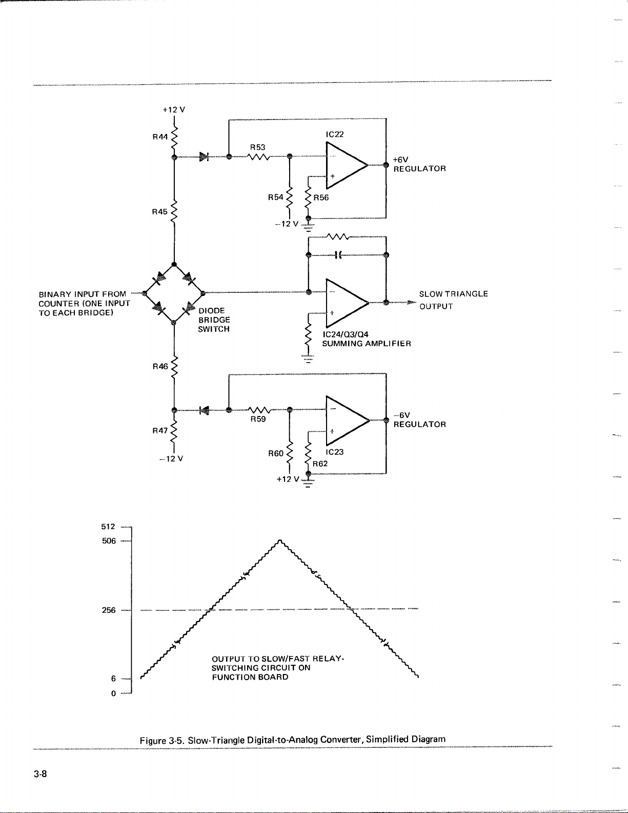
BINARY
COUNTER
TO
EACH
INPUT
(ONE
BRIDGE)
FROM
INPUT
+12V
IC24/Q3/Q4
SUMMING
AMPLIFIER
-12V
OUTPUTTO
SWITCHING
FUNCTION
Figure 3-5.Slow-Triangle
SLOW/FAST
CIRCUIT
BOARD
RELAY-
ON
Digital-to-Analog
Converter,
Simplified
Diagram
3-
8
Page 24
M
INTRODUCTION
-
This
section
calibrating,
instructions
electronics
a
factory-repair
possessing
maintain
the
problem
time
RECOMMENDED
the
factory
should
.
The
Model
stabilization
within
advance of
troubleshooting
checks,
errorinload
errorinthe output
provides
and
troubleshooting
are
concise
technician or
department
the necessary
instrument.If
for
repair,adetailed
be
attachedtofacilitate
157
requires
before
specified
useaprecise
tolerances.Prepare
any
planned
resistance
TEST
instructions
and
field
personnelortest
the
NOTE'
output
checkout,
programs.For amplitude
50-ohm
will
voltage
EQUIPMENT
for
testing,
the
Model
directed to
engineer.Wavetek
for
instrumentisreturned
descriptionofthe
one-hour
load.A
causea0
level
the
those
customers not
the
warmup
parameters
for
calibration,
0
.1-percent
.05-percent
.
experienced
equipment
turnaround
this
157.The
adjusting,
maintains
to
to
specific
for
are
in
or
calibration
checkout
following the
instrument
parameters
Electrical
point
layout
Preliminary
1.Set
2.Press
3.Wait
procedures
Specifications
and
diagramsinSection5.
The
entire
firsttodetermine
equipment
checkout
generator
the
1
hour
Setting
as
settingitto 0
procedures
procedure
can be
and
adjustment
Procedure
POWER
any
performedbyobserving
applying
calibration
connections
.
mode
for
warmup
rotary
.
for the
are
indicated
title.A
the
of
Section1.
locations
NO
procedure
initial
control
for
REMOTE
pushbutton
.
NOTE
digital
switch to
Model
tolerance factors giveninthe
are
7"E
before
.
157.Instrument
by a
quick
checkout
Circuit
shown
must
settings
attempting
.
R
is
the
checkmark-1/,
of
the
these indicated
board
test-
on the
be
and
board-
read
test
same
The
following
equipment.Any
maybesubstituted
Name
Oscilloscope
Plug-In
Electronic
Dialamatic
Extender
Distortion
*For
CHECKOUT
The
Unit
troubleshooting
following
table
Counter
Voltmeter
Board*
AnalyzerHewlett-Packard
AND
subparagraphs
containsalistofrecommended
test
equipment
for
those
Manufacturer
Tektronix
"Tektronix
Computer
Wavetek
Wavetek
.
CALIBRATION
having
listed
.
Measurements
provide
equal
complete
test
accuracies
Model
543B
Wor1A7
727D
201
157-111
332A
sequential
Power
Supply
1 .
Connect
inputtoTP1onthe
+12
2.Move
voltsdo±10mV.
3.Move
for+2.8
4.Move
common
5.Connect
inputtoTP6
6.Move
voltsdo±200
Square
Wave
1.Connect
to the
Regulation
the
voltsdo±10
voltmeter
voltmeter
volts
voltmeter
for
the
voltmeter
Offset
the
50S2
OUTPUT
voltmeter
do200mV.
---0.7voltsdo±100
voltmeter
.
Adjust
mV
and
voltmeter
high
power
mV
.
high
inputtoTP3
high
inputtoTP4
high
inputtoTP5
high
R50
for
connectiontoTP8
.
Amplitude
with
connector
inputtoTP2
supply
board.AdjustR7for
and
and
check
and
mV
.
inputtoTP7
--24
voltsdo±50
and
precise
on
50-ohm
rear
panel
and
check
check
and
check
terminator
.
the
for
logic
the
mV
for
low
-12
V
logic
low
.
+6
cc
Page 25

Terminator
50
ohms
.
2.Set
TERMINATED
generator
10
R5
3.Set
4.With
square
volts
5.With
square
Fast Triangle
Connect
1
.
terminatortothe
trols
peak-to-peak
2.Set the
function
3.Display
the peak
4.Set the output
the
mVofthe
5.Set
half-cycle
6.Set the
that
peak
NEGATIVE
Time
1.Set output
2.Set
mode
3.Connect
50-ohm
of
4
.
Set
channel.Position
waves
graticule.Use the
for
mode
.000
mHz,
on the
Output
output
function
voltmeter
wave,
±10mV.
voltmeter
wave,
Amplitude
the
set
for
FREQUENCY
for`L
the
a
at
Function
square
the
output
of the
output
the
triangle
.
PEAK
Symmetry
FREQUENCY
REMOTE
for
5052
terminator
oscilloscope
oscilloscope
with
more
accurate
voltage-comparison
negative
function
resistance
P-P
AUTO
for
output
and
Amplifier
toI
set
to
R34
adjust
settomeasure
R51
adjust
oscilloscope
5052
range
and10mV/cm
half-cycleofthe
convenient
function
Board
until
wave
function
square
function
peakiswithin
and
VCG
forI
dials
.
OUTPUT
and
(internal
for
the
the
axis
horizontal
observation
NOTE
mustbe±0
AMPLITUDE
CAL,
function
Board
measure
on the Function Board
for+5volts
with
OUTPUT
dials
for
reference
to
',v,and
the
triangle
.
peak
atrLand
wave
peakatthe
to
'v
5
Null
forR1.000
connector
T-connectortoboth
trigger)
100
psec/cm
two
bipolar
crossings
expansion,upto
.
percent
.1
dials
FREQUENCY
REMOTE.Adjust
for
for0volts
negative
positive
110
mV
precise
connector
measurement
sensitivity
100
.00Hzand
square
line
on the
adjust
peakiswithin
display
adjustR104
and
mV
of
the
POSITIVE
kHz
through
.
and
displayed square
about
midpoint
of
for10.0
dials
±2mV.
half-cycle
for
half-cycle
.
50-ohm
with
of
10-volt
.
output
wave
graticule
R111
positive
the
reference
square
PEAK
and
generator
precise
channels
invert
on
X100,
for
-5
con-
with
line
wave
one
the
on
V,
of
of
so
point
TP9
(first
the
.00
straight
for
symmetry
.
1000
.00Hzand
for
time
waveat10
square
waveat1
R01
.00
square
optimum
Adjustment
to
the
connector.Set
CAL
1000
.00Hzand
and Second
.
100
.00
.
optimum
within
both
the
and
the
counter
.
(ground)
VCG
short
kHz
kHz
kHz
kHz
5052
.
Frequency
Frequency
short
5.Momentarily
VCG/Integrator
and
node)
connecting
minimum
6.Set
7
8.Set the
9
10
.
5
.
11
Closed-Loop
1.Connect
2.Set
3.Set the
4.Set the
5.Repeat
Frequency
FREQUENCY
function
the
triangle
Adjust
required,
performing
Set the
.
function
the
square
the time
frequency
Set the
.
R79
for
frequency
of
.
Set the
R80
percent
Repeat
.
is
obtained
connector
countertoread
the
R43
on
Board
R20
for
obtained
If
frequencies
cation,
Alignment
Loop
Alignment
Do
during
observe
and
change
for
waveform
low-frequency
to
Steps
FREQUENCY
for
waveat100
FREQUENCY
symmetryofthe
range
FREQUENCY
time
FREQUENCY
for
time
of
frequency
Steps
.
Frequency
the
electronic
witha50-ohm
generator
FREQUENCY
Error
the
1000.0ftseconthe
for
FREQUENCY
10000
Steps3and4until
.
perform the
and
Frequency
again
Alignment
not
refertothe
the
following
test
Board
disconnecting
in
^v
.
observe
7 through 10
rL.Adjust
.
symmetryofthe
range
.
symmetry
7 through
period
mode
Amplifier/First
psec
on the
cannot be
then
Adjustment
.
TP10
to
display.Adjust
the
display
.
dials
for
Adjust
(Nullmeter)
R46
.
NO
TE
potentiometer
time
for
dials
R19
percentoffrequency
dials
square
dials
dials
of
range
.
10
counter
terminator
.
AUTO
for
dials
dials
counter
NOTE
adjusted
following
repeat
NO
TE
electronic
procedures
R01
for1.000
forR1.000
for
the
until
for
counter
for
:
on the
summing
R16
results
and
output
slopes
R1,
as
when
output
symmetry
range
observe
and
percent
and
percent
and
at0.1
wave
adjustment
~/
OUTPUT'
Decade
and
Hz
adjustment
specifi-
Closed-
display
until
in
on
of
.
of
adjust
adjust
the
adjust
adjust
is
4-
2
Page 26

8
1.Perform Steps2through
specified
the
and
2.Set
R21
on
3.Set
foranull
4.Repeat
obtained
5.Set the
foraclose-to-null
Trim
ment
6.Set
C3
Trim
ment
7.Set
C4
stepped
Meter
this
8.Set
frequency
MAN
CAL
adjusting
the
on the VCG/Integrator
the
the
the
foranull
the
for
range,
FREQUENCY
the
FREQUENCY
front-panel
FREQUENCY
indication
Steps
.
FREQUENCY
capacitors across
.
FREQUENCY
indication
capacitors acrossC3areafactory
.
FREQUENCY
smallest
through
indication
but
selection,
and
AUTO
indicated
dials
meter
.
dials
.
2
and3until
dialsto10
indicationonthe
NOTE
dialsto100
.
NOTE
dials
deviation
its
range
NOTE
normally
should
not peg
dialsto1000
below
simultaneously
CAL
potentiometer
for
Board
for
100
optimum
C31
areafactory
for
1000
from
.
will
.
by
making
pushbuttons
1000
.00Hzand
foranull
.00Hzand
.0000
front-panel
.000
.00
nullasfrequency
vary
widely
.00Hzand
depressed,
.
indication
adjust
adjustment
kHz
and
adjust-
kHz
and
adjust-
kHz
and
over
adjust
holding
adjust
check
meter
adjust
adjust
the
.
R99
R1
is
is
on
the
Error
Amplifier
deviationasdials
1000
.00Hz.
Sine
Conversion
With the
1
.
functionin1,,connect
oscilloscope to
2.Set
theFREQUENCY
R68, R93,
minimum
3.Set
the
R65
distortion
If
readjustmentofdistortion
or
balance
perform the
ment
4
.
Set the
measurement
mV/cm
5
.
Set the
function
6
.
Display
the peakata
7
.
Set output
Function
8.Set the output
positive
reference
and
generator
the
R15,
distortionofthe
FREQUENCY
and
R70
(approximately0.1
controls
Closed-Loop Frequency
.
oscilloscope
of
sensitivity
FREQUENCY
I
at
the
negative
convenient
functionat'\,,and
Board
until
half-cycleofthe
line
.
Board
are
changed to
Slow
Triangle
modeinAUTO
synthesizerasshowninFigure
dials
and
R6
dials
on
the
Counter
NOTE
are
controls
10-volts
.
dials
.
half-cycle
reference
sine
peakisat
function
for
990
.00Hzand
CAL
the
distortion
for
100
on
the
Function
sine
wave
.
100
for
required
peak-to-peak
for
at
square
.000Hzand
Board
percent)
analyzer
for
for
voltage-comparison
100
.00Hzwith
of the
lineonthe
adjust
reference
rL
wave
minimum
and
.00Hzand
for
.
frequency
this
Adjust-
range
square
and
meter
back
the
output
analyzer
R20
display
peakatthe
adjust
Board
adjust
minimum
step,
and
output
wave
with
graticule
on
line
.
and
4-1
for
10
the
the
to
.
.
Figure
4-1
.
Distortion
Analyzer
Test
Setup
TRIG
IN
4-
3
Page 27

9.Set
the
and
10.Repeat
sine
square
11.Repeat
output
the
sine
the
reference
Steps
half-cycles
half-cycle
Steps
mentisobtained
Trigger
1 .
Connect
50-ohm
2.Set
the
termination
the
Model
a.Generator
b.Output
c.FREQUENCY
d.TERMINATED
3.Adjust
stepped
peak
R74
do
voltage
down
Approximately5mV
function
peakishalfway
.
5 through 8
are within0.1
peaks
.
2 through 9
.
voltmeter
to
connector
controlsasfollows
157
in
mode
TRIG
functionin1,
dialsto1000
P-P
AMPLITUDE
on the
VCG/Integrator
changeasthe
through the
NOTE
changeisnormal
at'\-)and
between
until
the peak
percent
until
the
the
5052
.
.
Hz
.00
Board
FREQUENCY
to
100
range
adjust
original
its
values
(t5
optimum
OUTPUT
:
.
dialsat10
for
.00Hz.
.
R17
position
mV)
with
.0
minimum
dials
until
of the
of the
adjust-
the
V
.
are
Volts,-do
+5
.000
+4
.500
+4
.000
+3
.500
+3
.000
+2
.500
+2
.000
+1
.500
+1
.000
+0
.500
+0
.050
+0
.005
0
TROUBLESHOOTING
Interval,
Time
psec
1000
.0
1111
.1
1250
.0
1428
.6
1006
.7
.0
2000
2500
.0
3333
.3
5000
.0
10000
.0
100
.00
msec
1000.0msec
Frequency,
H
z
1000
900
800
700
600
500
400
300
200
100
10
1
0
Frequency
1.Connect
with the
to
2.With
function
Hz
Loop
measure
generator
Carefully
.
the
50-ohm
period
in
and Second
counter
3.Set
adjust
4.Set
adjust
5.Repeat
6.Repeat
7.Now
VCG
1.Set
dials
Connect
2
.
.
FREQUENCY
R119
FREQUENCY
R20
Steps
Steps
repeat
Sensitivity
Input
generator
R00
to
for
the
connector on
applied
.
3
.
Adjust
R69
psec(1kHz)onthe
4.Reduce
and
the
check the
best-straight-line
Calibration
Final
electronic
counter
termination
.
mode
in
AUTO
,
set
the
Ll
adjust
Decade
FREQUENCY
R43
Board
on
dialstoR90
11111.1psec
for
dialstoR99
10101.0psec,
3
and 4
until
optimum
2 and 4
the
until
Closed-Loop
mode
in
optimum
Frequency
REMOTE
.00Hz.
precisiondovoltage
the
on the
applied
panel
rear
VCG/Integrator
time
interval
do
voltagein0
frequency-vs-voltage
method
.
to
the
5052
connector.Set the
CAL
and
dialsto1000
the
Error
Amplifier/First
for
1000.0psec
.00
Hz
and
.
.00
Hz
and
settingisobtained
settingisobtained
Adjustment
and
FREQUENCY
sourcetothe
with
-+-5
.000-volts
Board
for
counter
.
.5-volt
decrements,
linearity,
OUTPUT
counter
output
.00
the
on
carefully
carefully
.
VCG
1000
using
the
IN
do
Basic
Troubleshooting
techniques.The
electronics
1 .
2
3
.
4.Visually
.
Troubleshooting
Table
symptoms
indicated
follow
localized
.0
given
voltages
associated
before
Techniques
the
following
fault
isolation
Check
incorrect
its
Check
.
that
correct
Perform the checkout
.
shaft,
associated
all
connector
control
control
will
connections
specification
recalibrating
check the
such
indicationsasbroken
loose
leads,
settings
setting,
causeafalse
equipment
.
indications
the
instrument
interior
etc
.
Chart
4-2
providesalistofsome
of
malfunctions
symptom
the
corresponding
to a
for
the major
at
passive
listedinColumn
specific
test
solid-state
elements
replacingasuspected
Model
157
requires
areafew
.
knob
:
that
carefully
a
or
indicationofa
connections
are
properly
procedures
can be
.
the
instrument.Look
of
wires,
charred
of
and
their
remedies
procedures
Whenafault
.
stagebychecking
points,
device
with
check
junction/pins.Check
ohmmeter
an
semiconductor
reminders
many
has
loosened
malfunction
:
connected
:
many
corrected
components,
the
more
.
1ofthe
the
the do
element
no
special
basic
of
times
make
sure
to
the
out-of-
for
probable
Locate the
chart
and
has
been
parameters
operating
(power
off)
.
an
on
.
by
4-4
Page 28

or
.
Table 4-2
TROUBLESHOOTING
CHART
Symptom
Automatic
open
loop
.
Automatic
on
some
loop
Generator
No
Poor time
Problems
No
rj
j
No
on
outputonlower
output on lower
and
'\,onlower
output
calibrationisless
calibration
ranges
only
operates
onsome
less
accurate
accurate
.
ranges
output on upper
symmetryoropen-loop
lower
sixorupper
six
ranges
six
six
four ranges
only
ranges
onlyordistorted
ranges
.
than
only
four
accuracy
.
only
than
open
.
ranges
.
.
.
only
Probable
Damaged
one
Damaged
Logic
Damaged
Cause
crystalorlogic
shot
.
error
failure
range
amplifier
range-divider
in
matrixorrelay
Failureintriangle-wave
MiscalibrationorfailureinVCG
.
Failure
slow-fast
in
Failureincounter
Failureinwaveform
Failureinpower
supply
failure
stages
buffer
relay
stages
logicorclock
DAC
.
.
in
crystal,
.
.
stage
.
circuitry
.
buffer
Board
One
Crystal
Error
Range
Range
Shot
Amplifier
Matrix
Matrix
VCG/Integrator
.
VCG/Integrator
VCG/Integrator
.
Counter
Counter
Power
Supply
No
'~,
output
No
Av
output
No
IJ
output
Asymmetrical
Distortedorno
and
-\,
Positive
waveform
Incorrect
Output
decades
or negative
only
output
amplitude
.
REPLACEMENT
.
.
.
amplitude
'1,
signaltosine
1,
produce0Vdc
half
.
output
cyclesofoutput
.
waveform
amplitude
incorrectbyoneormore
OFCIRCUIT
function
.
BOARDS
stage
stage
.
.
.
.
.
.
.
.
Boards
Defective
Defective
Defective
Square-wave
relay
.
Failure
Trigger
Output
.
Failureinoutput
Failure
function
function
function
sine
in
circuit
relay stage
clamp
converter
failure
relay
relay
faulty
.
amplifieratfault
attenuator
in final
attenuator
Replacing
Plug-In
Function
Function
Function
Function
Function
VCG/Integrator
Output
Output
Amplifier
amplifier
Attenuator
Refertothe
visual
aidtothe
Chassis
following
Assembly
procedural
illustration
instructions
Section5as
in
.
a
Plug-in
to
boardsinthe
rear
relativetothe
Model
last
digitofthe
157
are
color-coded
part
number
from
:
front
4-5
Page 29

PN
Digit
1
2
3
4
5
6
7
8
9
To
remove
.
Remove
1
the
rearofthe
at
front
retaining
Remove
2
.
shield
tion
shield
.
3.Pull
4.If
To
straight
remove
boardisto be
the
remove
boardtobe
the
top
connectorsofthe
Replacing
replace
1.Remove
?-.Remove
pushbutton
3.Remove
the
Left
4.Disconnect
5.Remove
Switch
Switch
Replacementisessentially
6
.
Replacing
replace
To
1 .
Remove
2.Disconnect
3.Remove
Switch
Color
Brown
Red
Orange
Yellow
Green
Blue
Violet
Gray
White
anyofthese boards,
the
three
unit
lip
.
the
four
over
the
on the
up
.
the
extender
checked.Then
Left
Switch
the
Left
Switch
top
cover
.
the
the
Switch
the
Board
Board
Right
the
top
the
Boardtothe
machine
two
switch to
one
machine
Board
the18Amphenol
four
to
.
Switch
Right
Switch Board, proceed
cover
.
the
11
four
machine
and
machine
plug-in
plug-in
checked
board
extender
Board
Board,
the
.
machine
the
subpanel
Board
Amphenol
machine
subpanel
Board
Extender
Output
Function
VCG/Integrator
Range
Error
One-shot
Power
Counter
proceedasfollows
screws
holding
slide
the
top
screws
and
screws
subpanel
screw
screws
the
screws
holding
boards
operationally
board
proceedasfollows
pin
reverseofremoval
pin
and
that
board
itinthe
put
plug
this
.
retaining
.
holding
connections
that
lift
and
connections
that secure
and
lift
Amplifier
the
cover
the
remove
you
with the
board
the
this
secure
out
follows
as
out
Amplifier
Matrix
Supply
:
top
cover
outofthe
calibra-
the
wish
to
unit,
position of
the
into
:
POWER
switch
.
the
Left
the
Left
.
:
.
the Right
the Right
to
Switch Board
4.Replacement
Replacing
replace
To
1.Remove
2.Remove
Unsolder
3
.
coaxial
conductor
4.Remove
uator
5.Replacement
REPLACEMENT
DECIMAL
decimal
The
one-half of
MTBF
for
20
million
during
rotary
followstoreplace
the
switch
1.Remove
2.Spring
3.Remove
screws
4.Remove
washers
5.Remove
6.Disconnect
front edgesofthe
7.Pull
10.Pull
11.Lamps
12
13.Replacementisessentially
off
8.Remove
9.Loosen
the
handles
Amphenol
left
and
and
pulling
Rotary
.
unsoldering
removed,asrequired)
now
obtainedbypulling
.
essentially
is
Attenuator
theAttenuator
top
all
the
connections
leadsatthe
the
Boardtothe
LAMPS
the
this
hours
life
top
out
all
.
the
that
the
the
the
all
the
right
can
switches
available.Access to
Board
cover
.
plug-in
boards
BNC
connections
(four
bottom
four
machine
rear
is
essentially
ROTARY
OF
lampsinthe
manufacturer's
lamp,
continuously
which
of the
itemisinadvertently
bail
the
side
machine
.
extrusion
pin
the
instrument
the
defective
and
bottom
from
bottom
front-panel
hex
three
hold
the
six
machine
eight
Mother
rails,
twoNo.
screwsonthe top
off,
leads
through
endsofthe
now
be
removedbyunsoldering
lamp
out
can
leads
from
off the switch
Board,
.
panel
precludes
covers
Mother
screws
Amphenol
startingatthe top edge
machine
6
from
now
top
and bottom
the
reverseofremoval
proceedasfollows
(three
leads),
the
Model
knobs
nuts,
Board
being
subpanel
be
the
the
and
of
the board
screws
retaining
andremove
reverse
of
SWITCHES,
157
voltage
item
of
Boardtoeach
(Left
switch-shaft
rating.The
operated
normal
However,ifa
.
damaged,
:
.
chassis
by
loosening
lockwashers,
each
from
pin
connectorsatthe
.
screws
carefultoguide
their
slotsatthe
.
the
rear
removed
RightSwitch
or
of
dial
reverseofremoval
leads),
the
five
.
the
board
the
removal
DIALS,
are
operated
in this
lamp
proceed
.
side
side
.
on each
and bottom
.
since
switch
locking
.
.
:
the
single-
Atten-
.
mode,
failure
lamp
their
and
rail
rail
handle
bottom
two
access
Board
wafers
nut
.
two
.
OR
at
rated
is
or
as
set
flat
.
.
.
of
the
leads
for
is
is
Page 30

SECTION
K
INTRODUCTION
This
section
Programmable
quick-access
a
arranged
viewing
data
able
schematic
are
schematic
included
and
and
ARRANGEMENT
Figures
and
procedures
Drawings
the
Title
Model
Model
Counter
Chassis
Mother
Extender
Output
Function
VCG/Integrator
Range
Error
Crystal
Power
Counter
Left
Right
Attenuator
for
the
schematic
package
parts
list;voltage,
diagram.The
numerically
diagram
in this
mechanical drawings
maintaining
5-1
through
internal
.
and
following order
Outline
157
157
Block
Logic
Assembly
Board
Board
AmplifierA8Data
BoardA9Data Package
MatrixAl1
Amplifier
Shot
One
Supply
Board
Switch
Board
Switch
Board
contains data
Waveform
document
the
user's
includesapart-location
coded
and
section
the
equipment
5-8ofthis
adjustments
packages
data
:
Drawing
Diagram
Diagram
(A1-A7)
A10
Data Package
Data
A12
Data Package
A13
A14
Data
A15
Data
Board
packages
Synthesizer.Each
that
contains
convenience
diagram
to
are
Package
Data Package
Package
and
waveform,
voltage,
correspond
that
Pacakge
waveform,
part-location
block
diagrams,
are
.
section
used
during
are
arrangedinthis
Data Package
Package
helpful
for the
supporting
illustration;replace-
and
with
calibration
Model
data
package
maintenance
in
simultaneously
data
logic
data;and
logic
and
numbers
illustration
diagrams,
logic
understanding
in
test
locate
and
section
DrawingNo.
157-603
157-600
157-602
157-000/200
157-010
157-011
157-012/212
157-013/213
157-014/214
157-015/215
157-016/216
157-017/217
157-018/218
157-019/219
157-020
157-021
157-024
.
on
.
points
157
data
Each
data
the
Also
test
in
is
a
LIST
The
electrical
items,
electrical
turerorfrom
electronic
time
ordering
ratings
the
criticalasan
circuit
A/B
Amelco
ARCO
CDE
Corning
CR
CTS
Elec/C
Erie
Fair
IRC
King..
MANUFACTURERS
OF
manufacturers
parts
such
as
parts
component
thanisrequired to
parts
agree
with
parts
lists.The
performance
. . . . ,,. ...
. . ...
. . ... ... . ... . . .
. . . ...
. . . . .
L
. . . . . . . ... . . . . ... . . . . .
. . . . . .
.
. . . .
. ... . . .
. ... . . . . . . . .
. ... . . .
. . . .
listed
in
listed
wire,
can be
Wavetek
locally,
installation
the
insulation,
obtained
However,
.
parts
order
make
the
values,
sizeofthe
at
higher
, ,,. . . . . ...
Teledyne
.
.
...
Cornel
. . . . . . . . .
. ... . . . . .
. ... . . . . .
. . . .
. . . . . ...
. . . . . . . . . .
Erie
below
make
following
can be
from
sure that
tolerances,
requirement,
frequencies
Federal
Fairchild
data
etc.are
from
the
many
purchased
the manufacturer.When
the
replacement
and
replacement
.
Milwaukee,
Amelco
Great
Dublier
Technological
Semiconductor
Mountain
. .
Broadview,
. . .
Neck,L.
Electronics
Pacific
Newark,
. .
.Cinch
Elk
Grove
..Corning
Bradford, Pennsylvania
DivisionofGlobe-Union
Milwaukee,
.
.CTS
Pasadena,
South
Electro
. .
.
Gabriel,
San
Erie,
Semiconductor
Palo
IRC,
Division
Philadelphia,
.King
Pasadena,
replaceable
the
packages
not
listed
of
partisnot
but
View,
Amphenol
Arco
Village,
Electronics,
Alto,
Electronics
.
listed.)All
manufac-
the
standard
locally
in
descriptions
may
effect
Bradley
Allen
Wisconsin
California
Illinois
Electronics
I.,New
Division
ElectronicCo.
New
Jersey
Mfg.Company
Illinois
Glass
Works
.Centralab
Wisconsin
California
Cube
California
Products,
Pennsylvania
California
TRW
of
Pennsylvania
California
(Bulk
less
part
only
Co
Corp
York
Inc
Inc
Inc
Corp
Inc
Inc
in
.
.
.
.
.
.
.
.
Page 31

Littelfuse
Mektron
Motorola.. . .
Mura
Nexus
Phipps
RCA
Richey.. . . ...
. . . . ... . .
. .
. .
.
. .
. ... .
.
. .
.. ...
.
.
. ... . .
. . . ... . .
.
.
.California
.
.Motorola
... . .
... .
.
. . .
.
. . .
.
. .
.
. .
.
Littelfuse
.
. .
General
Chula
Semiconductor
.
. . .
Great Neck,
.
Nexus
Canton,
Phipps
. .
Semiconductor
RCA
Somerville,
... . .
Incorporated
Plaines,
Des
Corporation,
Mektron
Vista,
Phoenix,
Mura
.
L
. I.,New
Research
Massachusetts
Precision
Nuys,
Van
Richey
Nashville,
Illinois
Inc
Division
California
Products
Arizona
Corporation
York
Inc
Lab,
Products
California
Division
Jersey
New
Electronics
Tennessee
.
.
Semtech
Sprague
Stack
TRW
USECO
Wakefield..
Wavetek
Winchester
. . . . .
. . . . . .
. . ... . .
. .
. . . .
... . . .
. . .
. . . . .
. ...
.
. . .
. . .
. .
... .
.
.
.
.TRW
. ... . .
.
. .
.
.
. . . . . . .
. ... ...
.
Electronic
.
. .
.
Newbury
Sprague
North
Stackpole
St
.
. .
Wakefield
.
Wakefield,
.
.
. .
Winchester
Semtech
Park,
Electronic
Adams,
Carbon
Marys,
.
Components
Camden,
. . .
.
.
Vernon,
Mt
Engineering,
. . . .
. .
San
Diego,
.
Litton
.
.
Electronic
Oakville,
Corporation
California
Company
Massachusetts
Company
Pennsylvania
Division
Jersey
New
USECO
.
Massachusetts
Connecticut
Inc
New
York
Inc
Wavetek
.
California
Industries
Division
.
.
Figure
5-1
Figure 5-2
Output
.
.
Amplifier
Function Board
Page 32

a`
%~~
~a~`~ y6~;
Figure 5-3
Figure 5-4
,L=
-P
L,
SUB
QIZM
PDD[F
6
0
VCG/Integrator
.
Range
.
Matrix
ILO"
,
LIIP
FA
Z
IA,
~v
,
Figure 5-5.Error
Amplifier
Page 33

xV
50
00
/
TPl
514
<OM
rP2
oar
eorrsa
A
N
p~xuneP
4
i
f
PNx
"
<RTSSw4T
*A
~
~~~
oeT
ee
®
An
fu~
Y
Y
Figure
5-6.Crystal
One
Shot
k
'^~
PT
h
.
t<
l~/
~~
h?
.___..
O
0
.®_._
TfT7
l~lll~oj+~
al~
,l(y~.y,
v
a.r
~PY
ed
Y\
!~,
. . . .
O
T37e'
A
mY6
l
~
~
oLY
N~
tib
7PB
40
TP/
Yr
3~°
ri'
¢
l
~~d
itiPlx
.3
TFS
l
llll
P
C'd'
7YL
B
Kc'~v
.Jl/l
LY~~6C
PVP
~
ti
\ x
ti
"
7112
t
~P
IDIT
YOa
.
1
yI
---
RA'
L
`N'hkNunea
SLOWA,OUT
RpV
fiLIN
T77'7'-~I
44DJ
L
BIT
A
.ao
TD~T
TP4
s,
.hr'(xuC~JJJ
Figure
£
DR
J
/
ITD
MT
Figure5
5-7.Power
Dd
TP4
5L-',
TPB
TSLODIT
.
Counter
.8
O
Supply
our
Board
66
IT
TPI
I
O
BV~csRFO
CLOCK
B
bJ/
N
i
ii/
C
l
Page 34

2
.x0
Page 35

____
----
-------
OUTPUT
INTO
CALIBRATED
SQA
MPEVANCE
LOAD
SYNC
Our
50A
AMPLITUDE
.82
5
TRIG
IN
16
.35
Re-diAw
tolerance
otherwise
XXX
X
Xt
scale
3/4
material
N/A
finish
N/A
unlessIrev
specubed
.010
t
.030
I
ecn
WAV
byBcrAKHI
q.Ioq,
title
OUTLINE
157
document
design
used
dwgno.
contains
rights
or repraduced
modelno.
this
and
not be
calibration,ope2tion
writtenauthoraation
Rear
'
rSK
date
DRAWING
L57-
belonglngtoWAVETEK
and
.
F65
by
san dlego,
F'a
603
proprietary
any
for
maintenance
12-A
date
app'
information
reason except
without
callf
may
and
Page 36

I
L
Page 37

-
INDICA
-
INDICATUS
."t'£5
51GNAL
PQOGR.AM
COMMON
COMMON
this
document
and
design
rights
notbeusedorreproduced
calibrabon,operation
written
authorization
proprietary information
contains
belongingtoWAVETEKand
and
.
for
any
reason except
maintenance
may
without
Page 38

V4
16
.?
~7
s
c
7
7e
0
7?4
'7,-4
I
~F
114A
--s
I-
4
V4
8
c
0
7Z4
0
/
724
17,
7
IZ4
Page 39

this
document
and
design
not be
used
calibration
written
authorization
contains
rights
belongingtoWAVETEK
or reproduced
,operation
proprietary information
for
any
maintenance
reason except
and
.
and
without
may
Page 40

a
~
.i
Page 41

01-iile
2l
BOTTOM
C64
COMER
SHIE4
IWAVETEK
D
I
WAVCTi<
l-3/2
A
i
-
-
~
OUT"ClUr
AUIVC7714V
VCG,
1AJr66,`P,9rOR
RANGE
'ANZA
OAIE
SHOT
POWER
COUNTER
-~AIWQOERI
141410LBOAUY
SE
MAMA
-
'WAV
80
SUPPLY
BD
ASSY
m5
FUss
-&a-
AiiY
fii4SSY
W-&K
9,SS'Y
8D
95ZV[vvlqvorr,-K
,
; f,
WAVE
-
WA
WAV67C,<
-
VIOW7jrX
NAME-A
I
w4venEx
I
INAVE-
Wr--K
I
WA
rEK
57
-15a
TiEK
17ZS8
-5
,h,documentcog,,,,",
d_'n
'i"ingIon'..gtoW~
and
be
isor
callbratg
not
written
reproduced
Operation
authorization
proprietary
and
.
for
any
maintenance
TEK
mason
and
except
without
t,
may
Page 42

:i~1~~~-rrrr
-J~J
SSSiS1>,S1SS1S11
~I
SS~1~19~ra11
SS1
.S~.;iZi
.1
S1l
NET-6-S'-'UNLESS
!
A-O.P,
i37-0100
Ire"
2
USE
,)tl-
~
:1-19
24
I57-SO&S
157-3078
~
i57-30BC
157-
Plwe4-
.2
svr"3
iS
BLI
30?C
OTHERWISE
.9ss'y
IVIC
DISC
SPCCUFIEO
SEE
FOle
DW6
sc,?EENIN6
Page 43

-
1TEM
_3_
ND
-EF
RlC>HT
Sus
REAR
_
poA~2D
/--/ANOLE
SUPAOQT
g0AQ0
. ...
.____
SWITCH
KNOB.CoAxlRC
LINE
DET~-Nf9"~.
ME"7
20
r'OTRNTloMETER!OK
FHSTENER
-/,p
23
DISC_
READ
,
.
27~.~
SWITCH
28
?9
MOTHc$rg0
tJEClMAL
3/
CEFTGlGHT-PO
,e~GNT
33
C
STANDOFF
8AlL<7S
36
ST"9N!_70FF
7
_3$
PARTS
DESCRIPTIOnl
.
I_
RAIL
SIDE
SlGE
PANEL
PANEL
_
SPFJCE,E
I
i
80,9Q0
SWITCHASSy
,2,BRALKeT
I,
MoDlFiED
n
r
I=AA/EL
onl
OUT
^
$D
LENS
r
04/4-3--
IGH
-
S
rl/
_
RAl~
LEr-r
RIGHT
Pu92
.._.
ASSY,
ASSY
.-
ASSY
_GllloE
LEFT
R
IGHT
BRACE
Ltt
SMALL
.
_
-
+~6-sZ
RlGNT
,
,
-
%z
/5
S~~lo
LAST
M_F__G_R
yvAvsr6<
Y,
. .
I
_°-~,
.='GE
_
.
CTS~.
GG_
_
.
~
,-c
CTS
--------ooors
AiecaACT
WAVErCK
LEFj
WAVE7reK
.°
.__
LAMPSI.OMS-24367
W,9vF7EK
T
"
BGCKEYE
W,4vET~Koi3-ao3-z
Mr-,RNO__
2110-3410
2/O-
___
/57-302
SEE
N07E
/57-324A__
/57
/57-3I3
_
l57
"
/E7.3/
/s7-3o48
A1S7
/57-3/7C
157
/S7-sW/
Talos
mI
I4i49Kl6778
_
So-l~'Sll2EMEM
30600
r8/o070
/S7"3000
/
.ST-329
20/-339C
2/O-356
/57
l57-l23
_
8480
342U
F
i
3/2f1-l^
ZA-Z
.3Z7
3/loB
-
.___.._.._14
_ _
020
-/ZZ
-
.q
°_
/
~l
c
/
~_
1
l
~
lO
._
/
6
I
I
SWITC
WAFF,?S
.,=I
ASSY(rVP),
MAY
40
r~CN!e80
ECN
56Z
tolerance
unless
otherwise
specified
~xxx
to
lo
030
~2EF~
EXCEPT
.2Y
1i
.9
NO.OF
IXXt.
scale
,V/A
material
N/A
finish
N/A
cue
model
/57
this
and
not
canbrabon,operahon
-tt~en
ecn
date
no
.
dwg
Dl57-000
I
document
contains
rights
design
be usedorreproduced
belongingtoWAVETEK
by date
can
j-8-69
~
.
no
.s>~6r2OF3
proprietary information
any
for
maintenance
and
die o,
ap
reason except
wdhout
and
I
app
calif
re°
G
may
Page 44

_--04-40WLX
4
4
~
h..
._
REF_
___~
.__
O^
21
22
~
1
23~
&
~?
F@
V
26
SOS
.
AMPLITUDE
ZjREP
2~
22
23
INTO
L
pU"1'PUT
Wr,
P,4VT
IMPEDANCE
CALIBRATED
LOAD
to-
-00
(7-YP)
J-1
05
0
G
0
VA
-
__
.~
~
~-
SYNC
114
(P!
I
REMOTE
MADE
~711
end
IN
USA
23
z2
0
L
TR
IG
IfJ
---
23
22
OUT
50000
ASee
0
6
0
tJo
14
)~
17
Z?
Page 45

I
/C)
I
l2
~
JCOA/A/er-'T6
-
--
r
AMP
--
T
-
--
--~
7
~203Z
T~-2o2663-9
73~-
-
2
T1
4OCK
AC
czll-
S,v
SsA-R,/OVG
socxers
COAhV--CrOR
xvr
SIWTCHCX4n
QA"OK
WIM
101926-/
__
Z'WC
3-G
jQxAv,v&2
A192--3i%
e
3
41
Yl
G
p4,,--5A*TN
--aGO
design
thus
document
and
not be
usedorreproduced
cahb,.tl_ P.
written
authorization
nights
.tion
contains
proprietary information
bo.."rig
and
mantenShce
.
for
.WAVE
any
may
T
d
reason except
without
Page 46

0404
04
m
h
-°O
_
)
.--o
08,
.p
06
02
CAL
MAN
AUTO
CAL
J9-
NN
0
°-O
04
-03
02
--
01
8
010
O
r-0
7
t°'O
s
05
04
04
®--0
3
~_
._0
1
OIO
C
9
09
a
08
7
6
3
2
r-O
7
_
.0
4
03
Oz
01
f
"O
-
O10
O9
08
07
O
OS
04
03
OZ
01
o
D
-010
E
09
08
0
7
o(,
05
4
0
03 02
02
O,
SEA~oH
--O
6
S
"O2
--°O9A
08
-0
7 °-°0
Ov
_
.0
S
04 04
0
3 3
-0
1
00
5
NI
I4
05
04
03
0
1
'R A
(~7w
010
_
.(\
0-
0
4
03
02
01
SVV7
O95O
0
8
7
-0
m
0
s
'_0
2
01 OI
00
Al
1-
.-0
C
G
9C~--O
08
--
07
-
._O
6
.
.,p
5
04 04
03
02
00
i
o
08
0
0
05
O5
04 04
03 03
0z
01 01
. .
._
._
. . ... . .
9
8
0
7
06
01
03
Z
0
0
1
00
09
7
Oz
08
-0
Ow
-O
04 04
'03
02
°01
Oo 00
7
5
08
_07
O(.
04
02
--01
00
3
06
-O
05
'"03
02
01
-O
_0
°OZ
7
o
O9
08
07
~
04
3
01
00
S
--0
05
0
B
08
07
_0
40
_
4
-
o
03 0s
02
j
0I 0I
0o
i^18
6
~9C
0
8
_
.0
0
O
6
05
4
04
03 03
02.
O1
00
O
O1
Oo
I
./b
9
8
7
(p
2
-p
--0
07
042,
02
00
D
h
R
D
8
!
R
.0
08
7
O
O
&
5
0
4
3
?
0
_-0I
00 00
h
_O9
08
_.-O7
O
m
-
.0
3
02
-
01 01
00
A
0
-07
.o
05
"'J3
0t
09
08
°p7
04
-
.0
3
-
02
00
8
0
®.".
-
.p<
1
,
01
O
;
"
O
:
O
9
g
6
Z
SW4
Page 47

SEE
SHEET
2,
_
R1,Ion
R2
$IS~s,1s
f
Swloc-W
SW6=-w
10
SEE
J
SEE
SEE
GET
SH
SHEE"
"
SHEET
"
SNEEi
,
.
C
T Z
2
.
B
Z
.
2
. .
O
B
09
~'
O8
D
-0q
r8
07
04,
OS
04
03
02
01
00
O
O
O
O
O
LR
.bi.b
O
~/
A
_
.~
3
0200"O3T°02
/
A4-9
C
p_
01
00
.____...._
As_
. .
GCN
SG2~
~L
.U3/B
,2E/lfBDSW06S
this
document
design
used
authonzatlon
contains
rights
or reproduced
and
not be
calibration,opemtion
written
proprietary
belongingtoWAVETEK
for
any
and
maintenance
.
information
and
may
reason except
without
Page 48

SHT
dl
Sn
I
ow'i
SEE
I
S",f
--3
~VLSip
ly-
SEE
SEE
NONE
swye-w
TKA-WO
SVv6o
:ff,
SM0
.--
wja--W
see
see
'
F-
F
Page 49

ONE
-'H()T
16A
fR
POWER
ria
,
8071
'SUPPLY
37A
,OMH7
F
T2
.p
-
-
4
c
SM%R
-&
8
M-A
2'~L
DECADE
UECADE
(c),10)
S
e
V
POOL
AMOY
swic-vv
-VV,
2
DECADE
4
--M,L
-X1
.p_
4
z
4-
I
4
LC)C)P
TZIr
i
~4TII
;GEP
DECADE
DECADE
r
REO
<o-a)
-EENOT-EL 1)
CCA\FreOL
CONTROL
>OL
-owl-
~j
5kiLk
Sk4p
ISNAUK
svv!SC
Sw
.5A-
-
-
w
KI
0
-
4
-QQQ-REC)
RED---
Al
214-Pam
-ks--4-
As-
3
~146-R
SW402
swc
pqnR
swaeA
R
Tl
yLq
R-
RYY9Pvd
i
svv
A
ST
14
:1
TF
A
2
I
AV
-
aP
~
AMPLI-:M
At,-,~LI71)[)E
FL
L
DEC
NO7E
ADE
?)
PEME41
Page 50

p
Ia
mg
mm
ro
J
33303o
7/-Z
e
I
r
I
2
24-P
14
J'-pEq
. .
.E
8
23'aDECADE
4FIZF~
DECADE
Q
DECADE
(0-9)
VA-0
,JZA-8
J7A~9
5'W-2
i
CaR
N
.
G2nl
~
vEL_
._
.,
R
SWU'
toy
-ZLOV
SWITCH
(SHOWNMIIOV
"~UJU6
POSITION
.
~4T"
z
14
F'kN
DECADE
Q
8
I
2
5r-"-
4
F
REQ
8
I
ZF2EgUEIvCY
4(SEE
8
CONTeOL
LOOP
T21GC,Elc
CONTROL
M"=1i-'LITllDE
tzANGES
NOTE`
(c-EP
(O-°J)
DECADE
(O-q)
HOTS
~J7Ya=~
.,o-
8U¬-_
17B-Is
RANGES
NOTES
I)
m
h
QI~~}_J
TIP
29
_
m
h h
o2
~''~}__.1Q3~rJLJ
TIP
:--E
ilh~h
y^~)
TIP
: h :
^
Ic
`
H
l
~
'1
'~
44
TI
Z)
ewe/wer
79B=i~=
w'EkiivT_
:UNLESS
0
---1000""
1
z
.__
._.__
4.
5
_ ._IOONL
6
. .
7-
.-
g.. ..
9
_ .
. .._.
'TO
PP,OG2/~M
CODE
OTHERWISE
._
._IOO,Hr_
-
. .
_
__
__
IS
1
P20GRAMFREOR.
S,PWL--RAlil
TRUEOR.
NOTg
FALSE
NoTr
FRONT
PROG2A),'IVIED
HZ
I
O
M
HL
1000
m
Hk
10
Hz
OUOI-+L
I
O
r
HL
.
I
OOKI-u
.
1000<14L
IG`Gf`i
8,1,+r
Y `
VOLTACoE
LO61C-
:
OV.51NKS-1'A
OR
I--OGI~
:
OPEN
CIRCUIT
ti.tzy
PANEL
SPECIFIED
Z
PROGRATrlAMP
FREO~AMP!';T"
INFORMATION
Ov=
`1`'
1V
V
TO+)OV
'V-+Z
VOLTAGE
OVERIDESAL(,-
INFORMATION
I_.-._.
2
-
I$
.__..
.--------
DEC
.ACF--S
--
10
(OO
--
(00
.
.__IOOOmv
THE
R,
my
mv
:
1BYOAT
OIE6D
_
.~~~
200
B~LONG~N6
FOR
C
CpuF
,e
.___l_._._
TO
CALIg,
OF'ERA-
REV
~ECr
ILKSAN
157
l
_..__
KF,
MAY
ANYREnSDN
zl
MAInJTFNgNC6
q'
li/II~x~
X57-
.
CONTAINSa)LOF'RIETAKY
RIUM$
u5ROORR¢PROOUC~
N(7i
8E
EzCEE'T
wIrNOUrW
_
WAVyBYB~MitFllatk`tE
Tr11E-~JCUMENT
INFOFa9A70~ifD'cSIGN
WAVE?g
FCR
Page 51

"64
.®~
(PS
,
Page 52

7°,O
7"YP
,eEFDES
aARTS
DESCRIPTiotii_
LIST°
__
MF{
.R
TKP
by
title
MOT-HER
no
.dwgno.
model
15
this
document
and
design
not be
used
cabbrahon,LOn
written
authorization
AtS
S'
IS?-C)10
contains
rightsbelonging
or
reproduced
and
,
`r
'
proprietary
to
tar
maintenance
any
information
Kan
reason
except
without
ca
may
Page 53

jj
5
/K7-,9,V
Page 54

ryp
rylp
finish
RED
WA_V
by/
,IA
~tib
tittle
NDEf?
EX
TG
.
. .
this
document
and
design
rightsbelongingtoWAVETEK
not be usedorreproduced
call
bration,operation
wrdten
authorization
rrA~~
If-
C
I I/
8~JARD
proprietary information
contains
and
maintenance
for
EN
any
'
;
and
may
reason except
without
Page 55

0
0
F
D
CS
C
3
C7,
C8
ca
C/,
CZC/o
Ca
&i9
2
A-/-
.e13
Q
lz
QlO
Qi3-Oi5
0/7-019
(221-
OZD,
6",
Q7,
Q5,
l7"OBa/
02
pa
CAOAC/roS75
CERAMIC
ELECTAYX
O/ODES
-_,
z
3
.4E
TRANS15
tS
9
09
DAP
DESCAQlRT1ON
/L0OV
zov
50V
Y17C
Fo66G
,4Y
FO~rM
r0R5
znl~oso.~oTOUx
2N22/9A
2N,7638
2N3638A
/OG
X08
.lcl-~
C
ON3
?N3905
TD/O/
ro4ol
TS
So
5Q7J1
6
703
1
/S
T
L
M
F(3R
CQG
SPf?AG(/~a
FAlFr~!ll
A
1/POS
/~Ni~D
SPRRGU
MF6R
DDO5o
1)0
/00
DO660
u*-zo-/0
F0~6C6
-5-8G5
z/vzgosq
3~1z2/9q
2n13(,38
ZN3(,38A
FN-
;903
2/V9905
rD/O/
ro4oi
NO
oao7
PARTS
EF.D
E
A'3
4
/ .
673
.FMS
R7/
oE5CRlPTloN
RESlSTOFrS
A~G1NICcJ
F/LM%s
TAC
5%
/O96620Aa
5%
J0°i
5
%
/03'o
4701L
; i
.
l
83/,1732
/
2
z
2
,Q17
.824,
Q/o,
R2
q7
R2E,
F~Z9,R3
R67K
FTl3,_R76
S,RB
R9~
.494
Zlo
/3
l
l
nr 'O
Rll,
lR2z
l?/o,RZ/
,Qi2,
F~23
`r
2/03
,4(
0
Rl,RZ
,Qa4
/0
3
3
3
f737
845,
Rl
R7a
2K-
;
KC3
o
6,
877
~15T
MFG
/012.0.WUL
/o0n
=
30
3
33
7
5
82
/S
/M
l4rc
CORNING
/,l.~
/ziK
.4
MFGR
Ai
20(aF/GYJl
RNIo
Zo
30/S
47/K
OD
NO
.
lOlT
l
J
821A'2
.302
332
75,71
BZz
153
1G5
2
ETgC
1
Z
~LMl+
2
Z
/3
Z
Z
Z
/
l
l
3
l
I
l
Page 56

x
6
f
~ri
1 4
~
~9RTS
5CP/PT/ON
iZti1A..
;l% 2/.5
'JSETJ2
IT`1OAlETE'
SINK
!ET
yiNAC
IT
CE~'D
.S
BOAF70
.~2n
~
2oon~w
/OoK
FUSE
/-
15
T
MFGRMFGRNO
QrrNlN(~
?IV60D
~
.41ET
~f7io4M
NF-207
20/08-/
/57-i/z0
GFA
/qA
.4~B
WgiVEFA&
hlWE7Z-Bl57-3/S
USECO
Ji1
~r,E(FU~
A
.
13
,
6
8
y
T%P
FOR
2
2
.3
.P24,
.Q29,
.Q3.Z4
2
:
.P25, .P28,
.P3P
tolerance
otherwise
xxx
xxt.030
unless
specified
t
.010
this
document
and
design
notbeused
calibration
written
rights
orreproduced
operation
authorization
containsproprietary
belongingtoWAVETEK
for
and
maintenance
.
information
and
reason
without
except
may
any
Page 57

1
ell
et
75
154<
-AS
,47
es
1OOK
,
9?4
tK.L
.
p
I
GA4
211
lOJL
^4
F1
plo
HE
ATSIAl
2N22/9A
7P2
.~
NOTES
UNLESS
w
MATCHED
MATCHED
'F72-1
-6
Im
-87--,
A
A&
oo
OrH,EAFPV,56
A-E
SFr
SET
-
---
llew,
0,-
OF
-
go(,
'e2]
-
S,-ECIF7EZ)
/0%
CAR80,V
a
-Zoo-rL,15y.7-0
/Y.7-0
I
L~---
---I
Ess
AW
RBb
2y-
(
V
.
jCRe
QN3E,48A
cps
M-1ac
CR17
e871Zf.SK
pus
L,--
I
I
t
I,J
-'Y
I
r-jI--
v
F2~ ?1/~j~-,nvn
Ax
1
z
LI
11,
Page 58

JUMRE,4
l15eo
oNLy
T//,!E
-
/70
248
ZK
e47
ZK
--
Nom
USED
ON
/-/W-170,-,-
2M3
200SL
254
2100
.3K
3
255
ZopzL
Ott
200
2008
D
R(,
-
9/7
ON
9~lO~llZ~l~i9~5,~6
f~~
T
NOT
USED
ON
THE/70
2~ozl
Zh5*
K,
/7
.~
LQ
J
%
;Cezs
K13
san
diego--,
aPD,~/
~E~
reason except
without
call'
may
finish
NIA
WA-V
_
bY/~ $OCNI_IJIDI
title
OUTPJT
th¢
and
not
calibration,oDemtion
written
".
SfHEMA
,4
COrvFl6tJRAT1ON
document
contains
design
rights
reproduced
be used
or
uuthonzaUOn
I',K
oat,
_3p_bg
T/
Al'1
PLlI
proprietary information
belongingtoWAVETEKand
'or
any
and
maintenance
.
Page 59

A~5F
C8
CZ,
C3
C19-CZZ
05,C/6
C17,CIS
C11,
C13
CC.C7
4,
C5,
CIO,
C/4
CRI-C17/
CB/3
ICl
SCZ
C3--Z-C/o
L{l-KG
Q7,O8
G2/O,Q//
Qi3
49,4/2
QlS
/
Q22,
027,a2e
030
32033
G24
Q
Q26
/4
/a
~9
DE5CR1OT1OA1
Cf!
Pf1C/
EA74A11C
5/LVER
CERAMIC
TFI41TAL
UN1
LECTf1aLYTic
"'VOLES
DIODE,
NTEGh'ATED
f7EL
AY
TRANSlST0
MICA
P
.4RT5
TOlQS
/000/
lOODV
FOla6(
Z6/VER
6BOFF
/OV
ZOV
/5bz2
1SV
/OO,Uf
Ci,4CUlTS
.45
2N3563
2N3G40
PN3638
5PF
/5f
470
68
1/ac
.uY
.(o
(-l8)
Cl5
MFG
C~46
ARCO
CQ6
.Uf
PFT
RICNEV
F9/lZ7'h/lCO
WVTK
RCS
pf1/GP,$
<Ai
T
R
.9GUE
.47?/l
MFG<?
ND
00050
OD/SO
OD470
DIMS-660J
DD
661
UA'i0-l01
611,Zo-/04
I9GDZZGXYo%S6'
lb
37500-/ST
FOlo&66
A13:)"
CA30r9
fA3030
C430--"g
~5-865
2N3563
VG
:5
-
zlv3e4o
P/
./3e,
38
o~,4rs
OTY
.
/
0
4
I?
2
2
?
3
0
/Z
2
/
/
4
6
.4EFDE5
C~l7,
OZ3
a2G
.02
Qcg1031
44,
-
03
Oi8
.45Ei
Rzg
A729 l5
,Pll7
R
4~,
4
//
RrlB
Z3,
ti'Z
RZ7,R3Z
7
/~lv
,2
.430
R38
A74
4~o"s
PS~
.R,Z
!?57
.
Z!kZ7
6
/l
A?2G,R31
RD4
R43,
R/07,
R110
R53,R6/
63,
R1L-
Rl29
R/3Z
.44/.R
Z
/O
R56
3
1454
G
T
.QANSlSTORS
QESl
AsrBON
0
. .
4
SCRiPTlON
ST0A75
fzr/
S°i
/O%
2/V3&4(o
2N3903
2N3905
5
/0%
5%750,
/0
.
536
/O
S%
ro12
391
471
62
IOOn
150-PL
~l~Orz
27052
33
4701
JGO
/.8
v
.
2
.7
3
4
6
9
.l
~isr
M%
FAlhC1vY
hl7T0
_
Z
H
.
.7
.Z
6,4
/,CY~IXG
MFGRNQ
Zn/39o
.3
21/3905
Ax?OGF/LV7
/sO
.3
4707
620
/O/T
l6
271
l5/K
/J
33/K
47/
S6/
75/
/82
20?
2Z2
33Z~r
472K
6Z2
9iZ
QTY
3
.9
/
,
Z
/
6
J
/
5
l
Z
4
3
1
2
2
2
6
4
/
l
R2
R74
R75,
l,
R3,
Re
RiQ
Rig
A7711772
W,NO
Rig,
RIi1
RBF_
R9O
R95,
RiOV
RiOI
/lZ
Rl7
F7i9.~5
a
_S
.R70
7F3,
rr$3
,481
R96
Rl25,Ri
R/
/
RBi
!lOZ
R5
R7
.
cri
o
,P33W39
Page 60

A9RT5C15
SCRlPTlON
STORS
YV
iz~
.llOY,lS.t'
~lCM%s,/
lWo
G
Z2
47
4y9
56
/Zion
3/bn
752711
82
l.7BA'
3
.0/
3.83
4
.32
Z1.sK
./9
l
l,~
.2
.211
Z
7.5
MFGR
lXt'ft
COBNlN6
.
.
T
MFGRNO
;YE
RN(o00
C~GF/S3
?Z3
/osn
14
P//R/7
SL15
RETG~s
M
P36
/O
/
l
.%Rl5
34,
R68,
roa
qr
2
~,
2
.37
'~~
GY~lENT/0,~1ETE<7
5i
R73
Rlll
~
TERMINfiC
C/
DESCRlPTlD/V
/OOn
75012
lOOK
r~'UiT
BOAf7D
MFGR
~C3PN~NG
A/B
Use-110
fJ4ET
T
.4
MFG
,PN~
~R/O/M
FRZS/M
FRlG~M
20/08-/
l/
.3C
/57-
/VO
R
3
6
l
17
l
7
3
©~~tLS~ItC~~
Z
6
tolerance
2
Z
/
2
3
2
otherwise
xxx
.x
x
scale
material
finish
specified
t
t030
Z//
N1
unless
.010
WAAveTEK
title
FUNCTION
modelno.
/57
this
and
notbeusedorreproduced
cahbraliun,opera[,on
wrrtten
dwgno.
document
design rights
authorization
,9157-013
contains
M
ecn
by
BOARD
proprietary
belongingtoWAVETEK
for
any
and
maintenance
.
M,
dale
-n
dnev,c-,,,
information
reason except
without
M/
app
and
may
Page 61

(Cve)
r
W
C~
'°
C24
CL
Cjl
C62
C25
lD,CZ6,C-C6
f23,
C'342,
C37,
C3
-:~Cd0
Cl
C4
C27C17,C30
C22,C
.35
/-Cl7
-ZCS
SCZ
,LC
G
Icl,3/4
All
-/Y6
CHGyClTGFrS
CERfl
.~4/C
-
5lLW,QA/4CA
ERI+M/C
/OGOV
1w&11--
.4F7NI1C
%S:W"
.
VLJRG9BCE
SELECTED
AjEGrRI
.OGYTk
Di00c
5
lllTEGRF~TElJ
cCAKA6~
RECAYS
P,9PTs
/DDO~
S~~
l5o
22PW
S/
E2or
9/OpF
l~l0
9/O(~
.6n?
/OVil,(l
~t7V..l,L(f
/OOY.Wf
2-6PF
VALUE
.
l5K
/m-F
./F~t/l
(-lb)
-l5
L
IST
C~?G
GO
p50
GDlSJ
DD2c0
D"1/5-820-
LRCO
OMlS-9//J
OM2^-972F
'DD222
7iRPv
C"?6
X663F
UklO-704
Uk20-10a
H-
-&a
EolE"
l28/
535-006-898
^
2/LhGYl6375-loo-l,ST
Aqcs7
RCFa
&90o4
RCA
llpRS
FDOW'
CA3D30
CA
:7039
MC8/6
CA3030
GS-864
.
0
POIYT:LIST
~
FrrOT/ON
DES
T~
.~r7rslsroAs
2
2
4
l
r
/
~
~7C
;G"Q
c
Cu'9
Q// 27/3903
Q/3
,QZ,Ol
~
Nl33C5368
a
2,3640
2N3iAb
2,,3905
TOlOI TDlOl 3
l
3
/o
l
P53,R5
l
1764
s
Z
/
l
/
R48,r?
RSZ,i-5
G16
R5/,G
R9,
4/4
<-~
F~~42,R47
773
r7
%?84
820,
R5o
RE9
R6O
6
.4t12,
r8,
lO,k3I
to
R73
,kb/
830
:+32
R25I
f?63
887
6
RES/s%
1080N
.
!,W
ORJ
/0/
5%
/50a
475
o8T
/0050
270n
470s
7
.5,(
/.8
3
5
6
lO
11
:
/
,
K
3
(
.Y
AiR_Nr
51664ZL
.
~
MFGR
22Nn39566338Z2
2NO640
2N
3'04'0
Z/V,?903
2,3905
-
-
NO.~T>'
3
CA
470
650
101T
5
271K
.K
47/
/02
7501'
/8M
Z
3
32
562
62'Z
7Q3 3
ll3
:
9
1
l
/
/
I?
2
/
2
2
S
5
7
2
Z
Page 62

P,~75
ESCRiGT/OrV
il.:TORS
l%l2K
7Nf/?H!
77
~3
lla
Q
.E
l5T
C
MFGR
IA~Kr?3C
MFGf~
Frt
~GCo~/23
NQ
273
33
llama
4~K
PXP75
A
EFD~S
/
/
/
DESCRlPTiDN
TERMINAL
4Cr%lTBa<iKD
C/
"
L
157-
MFGR
l/seco
A16'7,-6e'
MFGR
ZO/UB
/S
-//Q,4-
7
NO.~'
-//la
/
z
l
5IlO
L
:TEO
VALL4E
FlLM16~ly,
f
f
NTlOMETE~
Q2
Z.B7
3
.Oi
9,53
~s
lOGr
2
lCt'J
2~
l
(ORNlNG
A
B
R~/6UD
F'470/~
~
.425/M
f
~IOZM
~R/OaM
>?~7
l06~
i
¢
l
2
/
6
/
2
/
tolerance
unless
otherwise specd,ed
xxx
t
olo
.xxt
.030
l
l
l
(o
finish
EC/V
67,-'
EcN
440
~,oi
Rc
T
ecn
WAVETEK
title
model
157
this
and
not be
calibretiorn,operation
writtenauthorization
ASS/
vc
G
no
.
dwgno.
contains
document
dingo
rights
usedorreproduced
belongingtoWAVETEK
.JN
BoA1co
proprietary
for
and
maintenance
.
"M
MMM
by
san diego,
014
any
mom
dale
information
and
reason
without
app
calif
may
except
Page 63

°TP/o
__
TP9
29
470
.1L
1'
RI
IooK
0014
~T280
~'
diooK
C32
ISk",1
IM
R2
°..^M,
127
2
.4
11
%
1°6
RIO
~IK
Rio
Ik
+
C35
100
5Y
/VOrES
z
3
4
5
6
UNLESS
RESIST0
DIODES
)DELAY
ecL
--O
e
.lVMPtR
*-
.9YS
NloDFL
C43039
077-IERWISE
.2S
ARE
SHIECA
42E
SELECTED
f9AFE
PN/PPS
170
/2H!
8/0
/S
A-EMOli6
SPEGIF1EO
10,96
FOR
CARA90A/
KS
GOW
AND
LEAKAGE
ADD
r7
3a,~
K
,W~~
~~
~
QF
4VQ
~~
'
IV/
ov
A
&
oP
~r
~~LO
9
ti
l~oQ~
-4
a
ti
Page 64

RB°1
S
.I~K
.GZ
CA303q
R°70
nK
R38
OM
1
l5
c>_
aj
Pf
ZC5
O
ll
.
O
RB3~
1
.5K<
-a
0
I"SIC
R94P,
us
O
CASO30
CZI
,_,j
ASK
~!SPF
1100
I
osB~
,~~
o
oF
l0/l
btiy
~~J
2N3640
C
R73
6-2K
7
-
~l2/3r45/
fi
~
RIO
INtEer6Vb
AQW1,VVE2r1Mi
O
INPUTO-".
WPClr(
O
LOGIC
~
_
.'y
DIAGRAM
@
tycc
11
10
C,93030
t
-,
N,
LOC71C
DIAGRAM
MC8/loP
v
modelno.dwgno.
157,1`1701
this
document
contains
anon
and
.
proprietary
and
design
rightsbelongmgtoWAVE7EKand
not be usedorreproduced for
cahbration,operation
written
authon
any
maintenance
information
reason
without
may
except
Page 65

-
Rae
~P+-~R
14
---Cg;,$--
RIS
R2i
+-- RI6
1:Z'34
CR23
=-CLR24
-
CR2
'ik
5b7
'~07IAAFif!A
-
H9/0/l
--CRc4
cR27
cR2R~--
R30
AA
_
CR35---
CR37
/D
CR3
R31
cc
--
R
CR3
ce
l
c
IAO
11 /445/6 /7
A
32
n-%
A't
515
.
?
p[
I
A'._J
cRgl
...
.
,
Rs
--R4~~
R40J-~
"ii.
CR3
rtm1
:R54
QP
i
R49
(7
~
cR
J
R50
Q8
,~
ti
ti
I
R51
Q~
<
.
11433
CA4
--~CR58
R3--~-
~-
tR
-C
{-a3z
-
.-{
- .
.
R3
R30
Ras~-
;-
-~Ri
l~J
/"~
A
/0
REF
3,R
PARTS
DESC<?LPT1ON
MET,4L
TE,Q
.y~wA~
Ci~?CUiT
~~LMd4a;l~~
s
BOARD
"
;p
~~c
2
LIST
M~6R
CORNIN
usECO
li/Jt/E"TE
MFGR
RN60D
zoloo-i
157-//58
IVO
.
¢
l
Page 66

r-~~tt-cat
rVbTrm
K7
J
~
~QI
CR_6
~
R33
_r
}-
K6
4
4-
S
G4
-
K5
K3
T
rT
f7
.T
f
~C3
r-r
I
TTZ-'
111
K2
-
CRS
R27
CRbt
li
lZ 345b7
eaeB8
99~B
8
.Br
l3 l4iSl6
~ae~eB
/7
/8
~~
material
N
1A
REDRAWN
ecn
WAVETEK
title
14
S
S-,v
dwg
no
.
Di57-O/5
contains
and
.
MATf~IX
proprietary
to
maintenance
RANGE
modelno.
157
this
document
and
design
rightsbelonging,
not be usedorreprodudorany
cabbrab-,operalwn
written
authorization
by date
san diego,
WAVETEK
reason except
a
caht
rev
D
nlormation
and
without
pp
may
Page 67

015-1
A/
-
-
.-_
.,
a-
,e/
31C
RLL
/00
K
'R63,
TPI
JUMPER
/70
ontY
NOnES
0
2
01ODE,5
3
YRA
4
RZeAYS
s
Ic
B/0
G
T
.C6,,'8
UNLESS
S/S
s
Ape
/S44Y
427,
ARC
TACS
A'ze
RSZ
OrHE
V6664,
RZE
AZT6C
Mcesop
SIOC40
:?WlsE
ZN56BB
5pffcjFt
?O/So
l'23
4~5ER8
9
IO
~~OOQO
Eji2
1
000~~~~1
L~O~
0~~ 0
~A0
0
titF
7
,r
O
~o
O~-A-.,. ...
SGS
Page 68

.
.
,
B/
92
83--
B4-
R41
1OOK
--0/4
/3
rO
/2
'
0
~
.~~tiahPYy
.cc
.
.y
¢~,
PP
`~
d)a'OBI
L
ON
VSEO
i70
0)
.
6--l
5
7
1
l_OG/C
MC
x ~
r
.
890'
/-,-
°
DIAGRAM
~~O
.69
1
8
this
document
and
design
riAhts
not be used or
calibration,operatan
Written
auth rratTo^_
proprietary information
contams
belongingtoWAVETEK
for
mid
any
maintenance
reproduced
re-
and
except
without
may
Page 69

IUD
77
PARTS
CN
~E
3
l
P
2
l
z
Z0
9
LJ5!5
k~F
R3,RII
RZZ
RIZ
RiB,Rl2/
RZ,R1O,Rl7
,?4
.3O,R33
R9lo,R39
R4?,
R45
RR54
R23
RllSI
DESCRI
RESTS
CARBOnl
Sl
R/3
R19,
RIZZ
R2/
R93
R&
2
l
/
PTIOlV
r02
s%"
l/zw
/O%,820.0.
590,BK
I
I
10q,3"
lOYo,
IOgo,Z
47CL
/OO1L
/K
I-$K
3K
S%S.lK
/OK
ZZK
l/OK
lM1L
241,41
.?~NA
LIST
MFGRMKGRNO
SMCKPOZE
RCZOGr470
.7
1017
82IK
loz,e
IS2K
3OZ
.7
332K
5/2.rl
/03K
2Z3K
ll4K
/05K
243
T
205K
REF
055
R
Z
/
J
2
3
I
9
l
/
l
2
l
l
R78,R8o
"'BP
RB4
,e8~,RBB
R7
R8,R9
R14
-,elb
.%7R68
ego,
RgI
R77,
R81
R83,,Pf
R87,'89
RS-6,
R60
R6Z,R65
R66
013
R75,
,P77
P57"R39
R61
R63
R6'l,e7Z
P74
R7(o
R7/
M
w
I
w
w/
M
W
"
N
w
N
W
2
Z
Z
1
2
RS-P3/
,?3I,
R37
R46
,¢40,
,P4$,P51,
kl
P3Z,,P3S
R47,
RSO
R53,
PS6
,244
METRGf7LM,
l~Pw,
~
lY.2K
T
~C99C
69gK
CORMNG
RN600
I
I
9
C
l
/P//5
/
5
EF
l,
C3,C7
C//'MYLAI7
C2,
C6
6/0
C4,
GS
C5,
C9
,
=F1
L~
r
nC~-,r9
ICl,ZC2
IG3 46W
IC4
234
'9
AA4AA.<7A
799/0ll!?13/01516
o79RTS
GESCf~IPTlON
D
CAV
.4l'/TOF7S
/GW'
ER4MlC
E~A
.~IIC
Mf'LAR
EC
r~Y17C,l5V100,v
EL
D/ODE
3
RELAY;;
LVrE6RATEDCl,4`ulryA7mFAikrNi~D
LAAKACC
d
2xJGrCRG
ewV
50~"Oll/
Poll
r%
~P7V
FOblorolo
Faemr
(-/8)
MC145&
.3
W
LU!
C
fly
MFGR
TA?J
.,/
CRL
;
C
L/SC
,4/CIIEY
F+7~,elMCG
PH/PPSP5
ktA
40rAP0<A
AfJAANA
T
MF6R
002?/
X~lo9F
CA-I03
UK20-/OQ
2706/C"'OSF
/6-37&/00-/5r
Fb6~oleo
865
"A709
C,9303'f
ACA456
TRANSISTORS
ZI
36H
ZA13905
ZN3638 7
FR
1
.92*
FR/04M
ql,
03-0
Q8~
R99, Rl
r?ZL)
O//
OZ
QIO
R43
6
J9FbreA
rlOML-TE2
2N3638A
2Ak905
ZN36
/OO,<
.38
/AC
AMrOeo49
FAIRCHILD
,91,
6
91,6
RC%R9t
METR6FiLM,
-,,
IV,
49y
l
CO&N/A/!
RNSSO
Z
Page 70

DESCRIPT7ON
L
K
S
QESi5
MRS
80
64
1
88
AaETgCF1cM
MArfM90
r/4w"lY°
SET
76WhPEjV0UW0
~1
4w
,oZS°/
,89/Wi2EWOUAID
f4W
/%
WIPEWOUNO
91
B6
law../9r
39
X60
77
'59
Z
~~
.
MfT
:HEO
SET
Wye6w0IJN0
h4RTCHEO
WIREWUWO
94w
MA7rNED
WIEEWMNO.iW.O1%,7Z
O~S~
SET(23)
SET
TEPMiivi7GS
GiPCUir
BD
S"sCKrEOINCAC.la
PARTS
.~OJK
(-26)
3
40K
40K
23)
40C
4oK
2d1
Z
"
Mfx2R
COeNi~Vb
MEKTRON
.t
USECO
WAVE7ZW
c/
9T
MFG
.2
NO
,02
1PN60D
MK
;3
I
i
l
j
I
20i0B-l
157-ll6G
S
4
~o
8
8
l
tolerance
unless
otherwise
specified
xxx
t
.o to
l
O
4e
To
El-EE
IN
PIN
CAL1,B,2I9TIO~V
.P
1
PW
T
xxt.oso
material
MIA
finish
NIA
WAVETEK
by
iIXNKHIO
title
FPA>OR
modelno.
1,57
this
and
not
canbration
wtten
ecn
ASSY
A,WPL)AE"R
dwgno.
Dl57-D/6
document
contains
desigrr.¢hisbelongingtoWAVETEKand
be usedorreproduced
aut
operuhon
honZaUOn
and
.
by
San diego
proprietary
any
for
maintenance
date
ntormation
reason
without
app
calif
may
except
Page 71

-513
Rl"a
-
NOK
A*--
-N4
-B6
I
I"'f
RIB
22K
Rsk
a
Rfid
B
3
-f
-C-1,
A
Rl?_
Wo
R
Roo
BAY
.
--
3"K
Rss
ZK
I*/.
54
oml
6
ki
Bb
__
OXES-u
i
.ALL
R
?
.AWL
I'
4.SWEL
Ae.
5g
MIS
PIwI
C
q*
am
7CQTH
S.ff
CAJe
O
I
7
-
L7C_
OUTPUT
OFFSET
- vvtcc_
MC_
DIAC,(2AM
145(o
LOGIC
Page 72

5
~9
s
.2K
WW
n
"
025,°U
3
n
R:Ia
.2K
,0259
WW
°'~
TC4
MC
1456
_
S
S
C9
ZOOV
I
NE
\
l
2115
TQIM
CIO
.Iuf
2OV
A-40K
K-.01
8
-40
C
-40K
.0251*WW(6MATCHED
0-40K
E-301K
I%WW
W(BMATCHED
Wo
W
.I%WW(6
1%
(6
MATCHED
(4)
MATCHED
TO
.002°
.6
TO
.01%)
TO
.01%)
TO
.1%)
~--4LL
s1_l..
RLl
.
HIELD5
~'
2115 1-0
P.JI
JUMPERS
A3
THRU
q
CA3037
UNLESS
RESISTORS
\°,~,
RES\S5-ORS
DIODE.
OF
FeE
02
CI7
SELEC>EO
100]1`If12Y[
OTHERVJ\~.SPF
V?W
ARE
FOGGrs4
FZCl
.AYS
B9
CONNCCTCO
IN
CALIBRATION
USED
OH
USED
ON
F6R
1114
Npro.N
.,C-\DIED
1017.CARBON
1/4WATT
TO
GO
TO
ONLY
170
170
ONLY
LOW
LEAKAGE
°
FI5~16~
"
R91CR~~R13
`}79
A,`,
R119
A17
A18
17118
w
9f
qJ
l
y
A10
BII121x1415
[10
1
819°
o
aSop
S~
i12~13.~1A
~15,~6~17~~IB
ti
OJ
O
A
J
A`
G~
.
O
4y
tolerance
otherwise
scale
Z,4l1
unless
specified
XXXI.010
.XXf
.030
NONE
R
698K
ECN
Ss-o
G
2svlsso
ADD
F
ADD
D
ADD
C
ADD
B
ADD
REDRAW
..~.
C73
rHRU
CI7
cll-R12t-Rt22
47n
ASS'YFGS2-13°69
AMP
170-OPTION
LOGIC--
3/7q
F65
4-IB-69
F63
3-13-L9
P65
2-24-M
F6S
1-30-69
_°_~-
(PIN4COWECTEDTOCASE
Lor-lc
D\YAGRAM
-yA70q
F02
E
a01B
SCHEM
reason
I14
and
except
without
.
re,
may
LATEST
.)
DE-91GNATOR
COMPONENT
USED
IC4
CR
25
1
2
C
R
120
12
Q
W9
Fi2ECZUENGY
modelno.dwgno.
15-7
this
document
and
design
not be usedorreproduced
cahbration,operatlon
written
authorization
UEGADE
ID157-21(o
contains
rights
belongingtoWAVETEK
and
.
proprietary information
for
any
maintenance
Page 73

IC30
CA5C
:'9
MCB24F
i0ICl2
F-7
-
MC825,
q
r
«~-
C3
/
T22CPf
.4
I
Sn
Q4
2N3638
Page 74

-
4
0
9
7
RE
8
3
TP5
R34
23
.7K
I%
3901
R29
11
23
.7K
TP6
R30
12
.IK
R22
.t
ME6
R23
2
.
K
!%
R24
6.19K
R16
R
;7
_-GND
7
R!8
3AK
ty
-~
-ilc2~'
.
IC21
MCBBBP
"`\5
TP7
.ro
G.I
~
IR77I
n
_
.-
Yt
c(1
I
R
6anl
TB,
MG892P
I\
_
c
e
TP8
R2
1
.3 K
%
:
_
CC
'T-SJ-lI
~_
~-
.~
R5L
27 RS
SK
!%
iT
r
I l
L__In_
R6
!
.5K
I%a
._.A.._.ty
C
l
DD
825P
'\
MC824P
is
e
MC89CP
TPI
O
rc
0_,t
MC892P
6
MC892P
~12~,..
5
IC8
MC824P
\-~e
ICIS
._
. ... .
91
F6S
$-27,6qq
FGS
2-15-d~
-DATE
BY
.,q
B2
;APP
._.._
7P9--j
a
ICS
NIC
B90P
j316
tolerance
otherwise
N/A
finish
N/A
!6J
I
o
B14
unless
specified
this
and
not be usedorreproduced
callbratlon,operatlon
written
COUNTER
dwgno.
document
design rights
authorization
MC824P
MCB92P
contains
belongingtoWAVETEKand
12
Bib
TP2
f
NOTES
I .*LOGIC3.6V
2
.
3.+If
4.Bi6
MCB25P
MC824P
~_~IC13
MC825P
'IC
UNLESS
2TOPINS2~6
(10)
MATCHED
I0
WITHIN.2
LOGIC
PINS
(4
(3-4-5
ZC~-6-IOIC9-14,LC16)
(4-5-14
IC17~2-4-5-G
2-3-4-5-6
l)
IC20
0°
FROM
COMMON
IC6-8-14-IB-20)
IC211)
MC824P
ZC
:3
_-
19
5
I64
NIC
89cp
c 0
"^C624P
IC
9
~10
OTHERWISE
B17
ICI
RESISTORS
I/eiOF3
CONNECTS
(4-5-7-10-12
MC824P
_~2IC12
MC824P
IC13
12
N
PIN
TO
THRU
IC5
3
.OIK
.01K
4-6
2-6-13
(4-6-9-12ICIO-i3)
ICI)
19)
i
SPECIFIED
II
70
ICII
MCP
B24
1IC
14
MC824p
r
IILl4
MC824P
ICI
THRU
MATCHED
THE/FOLLOWING
C~-10-12
ZC12)
13
5
IC4
MG
890P
o
~P4t0`
pP
"
O
,>R
22
IC
TOt.05%
IC2-3-4-5)
ICIS)
9
MC823
IC7
MCB24P
IC14
-
'
~MC825Pl
4
P
,
__~lIICS
4
~I
5
^
B9oP
(7YP'
Vc
12--
(TYA
(TYP)
proprietary information
for
any
reason except
maintenance
and
.
may
without
Page 75

~Ii
/I
Ql
F
DES
5WlS
REMOTE
0
0
0
DESCRIPTION
.9G31
.~~Tt7<?
C
Tf7AN5/STDR
SWI4
sftiFro
PARTS
I
LIST
MFG/4
'
~lLxHILD
,5W/3
TRiv
I
-6.4
2//36GZ
SYj'/2
A"7-0
CAC
000
NO
Q
SW//
l
M4n'
CAL
00
aosr-Ul
000
RESISTOR
R8 RBON
R~
Rl
R7
R3~
Rq
R2
RS
SW115*12
SWi3,
SIY~S
ETAL~lLlgi'J,
AMP
SH/iTCN
SWi4
Cl~UlT
fz~.:S`Y
Ia
w~
/o/
.~l+l,7.3 ~Q9N/NG
A'NS
A55
BOARD
lOZ
.33Z
lS9
903,
33
42/
.c'
l
,
l
2
l
/
l
/7
l
7n
~7AC
.(~
4
l
%
3
3
.3D
RCt~GF4Xl
gN60G
AMO
K
WAVE
6o3~s-l
8/
.5-7
/57-1200
Page 76

tolerance
otherwise
.xxx
xx
scale
unless
specified
olo
.
t
roao
_Ee_N_3_i8
REDRAWN
A
rv~`ecn
Wir
YEflo",vw
title
LEF7-S
this
document
and
design
rights
not be
used
calibration
,operat'on
written
authonzation
_
K
A55ly
W1TCf-H
wgno.
Z/57-OZO
contains
v
proprietary
belonging,toWAVE
or reproduced or
and
maintenance
.
z
.
.bydateof
san
diego,
BD
,
information
rEKand
any
reason except
without
ca
rev
may
Page 77

N
-Ai
PAPT5
Z157'
CAR
Do/o/
IVO
07Y
Page 78

this
document
design
used
authorization
contams
rights
or reproduced for
and
not be
calibration,operahon
written
proprietary
belonging
and maintenance
.
to
WAVETEK
any
"format-.on
and
may
reason except
without
Page 79

Fp66
,6
Page 80

tolerance
otherwise
xxx
Axf.030
scale
material
,mesh
unless
specified
t010^v
ZXl
.
by
E
title
AT7Eil~U"4TOR
modelno.
/57
this
and
not be used
callbration,operatlon
written
Vv
oIAHlq
document
design rights
authorization
K
-r
date(
649,
Ass
contains
proprietary
belongingtoWAVETEKand
or
reproduced
for
and
maintenance
sa_n d_e
BOARD
any
go,ca~lif
information
reason
without
may
except
 Loading...