Vishay VS-10UT10, VS-10WT10FN Data Sheet

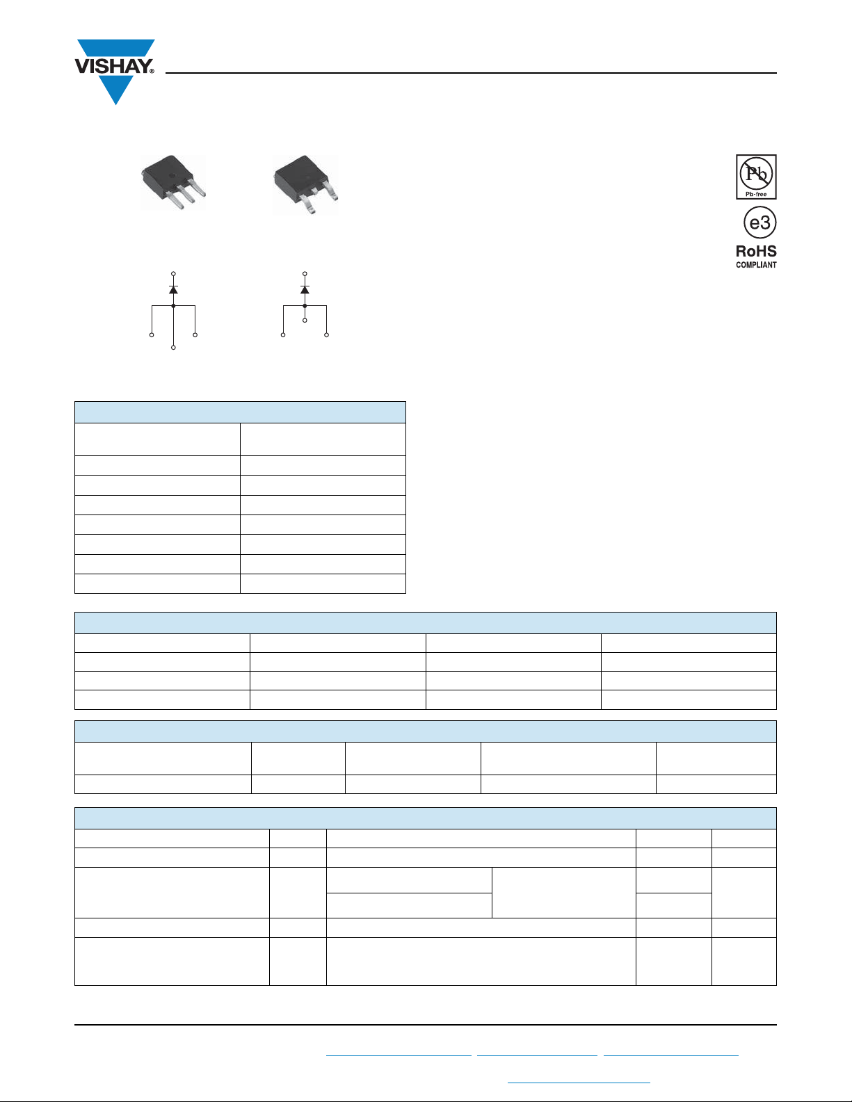
I-PAK (TO-251AA)
D-PAK (TO-252AA)
VS-10UT10 VS-10WT10FN
Base
cathode
Anode Anode
Cathode
4
3
2
1
Base
cathode
Anode Anode
Cathode
4
3
2
1
VS-10UT10, VS-10WT10FN
www.vishay.com
Vishay Semiconductors
High Performance Generation 5.0 Schottky Rectifier, 10 A
FEATURES
• 175 °C high performance Schottky diode
• Very low forward voltage drop
• Extremely low reverse leakage
• Optimized V
• Increased ruggedness for reverse avalanche
capability
• RBSOA available
• Negligible switching losses
• Submicron trench technology
• Compliant to RoHS Directive 2002/95/EC
• Designed and qualified according to JEDEC-JESD47
vs. IR trade off for high efficiency
F
PRODUCT SUMMARY
Package
I
F(AV)
V
R
V
at I
F
F
max. 4 mA at 125 °C
I
RM
T
max. 175 °C
J
Diode variation Single die
E
AS
I-PAK (TO-251AA),
D-PAK (TO-252AA)
10 A
100 V
0.66 V
54 mJ
APPLICATIONS
• High efficiency SMPS
• High frequency switching
• Output rectification
• Reverse battery protection
• Freewheeling
• DC/DC systems
• Increased power density systems
MAJOR RATINGS AND CHARACTERISTICS
SYMBOL CHARACTERISTICS VALUES UNITS
V
V
T
RRM
F
J
10 Apk, TJ = 125 °C (typical) 0.615 V
Range - 55 to 175 °C
100 V
VOLTAGE RATINGS
PARAMETER SYMBOL TEST CONDITIONS
Maximum DC reverse voltage V
R
TJ = 25 °C 100 V
VS-10UT10
VS-10WT10FN
UNITS
ABSOLUTE MAXIMUM RATINGS
PARAMETER SYMBOL TEST CONDITIONS VALUES UNITS
Maximum average forward current I
Maximum peak one cycle
non-repetitive surge current
Non-repetitive avalanche energy E
Repetitive avalanche current I
Note
(1)
Measured connecting 2 anode pins
Revision: 10-Aug-11
For technical questions within your region: DiodesAmericas@vishay.com
THIS DOCUMENT IS SUBJECT TO CHANGE WITHOUT NOTICE. THE PRODUCTS DESCRIBED HEREIN AND THIS DOCUMENT
F(AV)
I
FSM
50 % duty cycle at TC = 159 °C, rectangular waveform 10 A
5 μs sine or 3 μs rect. pulse
Following any rated load
condition and with rated
10 ms sine or 6 ms rect. pulse 110
TJ = 25 °C, IAS = 3 A, L = 12 mH 54 mJ
AS
V
RRM
applied
(1)
Limited by frequency of operation and time pulse duration
AR
so that T
< TJ max. IAS at TJ max. as a function of time pulse
J
(see fig. 8)
1
, DiodesAsia@vishay.com, DiodesEurope@vishay.com
ARE SUBJECT TO SPECIFIC DISCLAIMERS, SET FORTH AT www.vishay.com/doc?91000
610
A
at
I
T
J
AS
max.
A
Document Number: 94647

I
R
- Reverse Current (mA)
VR - Reverse Voltage (V)
020406080100
0.0001
0.001
0.01
0.1
1
10
100
25 °C
175 °C
150 °C
125 °C
100 °C
75 °C
50 °C
VS-10UT10, VS-10WT10FN
www.vishay.com
ELECTRICAL SPECIFICATIONS
PARAMETER SYMBOL TEST CONDITIONS TYP. MAX. UNITS
5 A
T
10 A 0.735 0.810
Forward voltage drop V
FM
(1)(2)
5 A
20 A 0.840 0.890
10 A 0.615 0.660
20 A 0.730 0.770
Reverse leakage current I
Junction capacitance C
Series inductance L
RM
T
J
VR = 5 VDC (test signal range 100 kHz to 1 MHz), 25 °C 400 - pF
T
Measured lead to lead 5 mm from package body 8.0 - nH
S
TJ = 25 °C
(1)
Maximum voltage rate of change dV/dt Rated V
Notes
(1)
Pulse width < 300 μs, duty cycle < 2 %
(2)
Only 1 anode pin connected
= 125 °C - 4 mA
R
= 25 °C
J
T
= 125 °C
J
V
= Rated VR
R
Vishay Semiconductors
0.630 -
0.530 -
-50μA
- 10 000 V/μs
V
THERMAL - MECHANICAL SPECIFICATIONS
PARAMETER SYMBOL TEST CONDITIONS VALUES UNITS
Maximum junction and
storage temperature range
Maximum thermal resistance,
junction to case
Typical thermal resistance,
case to heatsink
Approximate weight
Marking device
100
TJ = 175 °C
10
TJ = 125 °C
TJ = 25 °C
, T
T
J
Stg
R
DC operation 2
thJC
R
thCS
Case style I-PAK 10UT10
Case style D-PAK 10WT10FN
- 55 to 175 °C
°C/W
0.3
0.3 g
0.01 oz.
Revision: 10-Aug-11
1
- Instantaneous Forward Current (A)
F
I
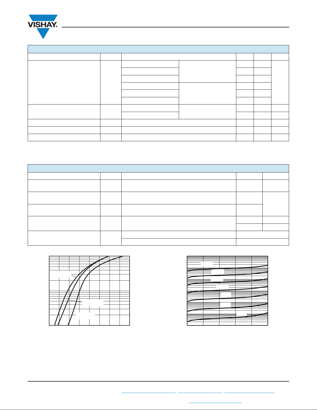
Fig. 1 - Maximum Forward Voltage Drop Characteristics Fig. 2 - Typical Values of Reverse Current vs.
For technical questions within your region: DiodesAmericas@vishay.com
THIS DOCUMENT IS SUBJECT TO CHANGE WITHOUT NOTICE. THE PRODUCTS DESCRIBED HEREIN AND THIS DOCUMENT
0.2 0.4 0.6 0.8 1.0 1.2 1.61.4 1.8
VFM - Forward Voltage Drop (V)
ARE SUBJECT TO SPECIFIC DISCLAIMERS, SET FORTH AT www.vishay.com/doc?91000
Reverse Voltage
2
Document Number: 94647
, DiodesAsia@vishay.com, DiodesEurope@vishay.com

www.vishay.com
C
T
- Junction Capacitance (pF)
VR - Reverse Voltage (V)
02040 8060 100
10
1000
100
0.01
0.1
1
10
0.00001 0.0001 0.001 0.01 0.1
t1 - Rectangular Pulse Duration (s)
Z
thJC
- Thermal Impedance (°C/W)
1
Single pulse
(thermal resistance)
D = 0.75
D = 0.50
D = 0.33
D = 0.25
D = 0.20
Allowable Case Temperature (°C)
I
F(AV)
Average Forward Current (A)
86421210 14
16
0
165
175
180
145
155
160
170
150
Square wave (D = 0.50)
80 % rated V
R
applied
See note (1)
DC
Average Power Loss (W)
I
F(AV)
- Average Forward Current (A)
12963
15
0
8
10
0
4
6
2
180°
120°
90°
60°
30°
RMS limit
DC
VS-10UT10, VS-10WT10FN
Vishay Semiconductors
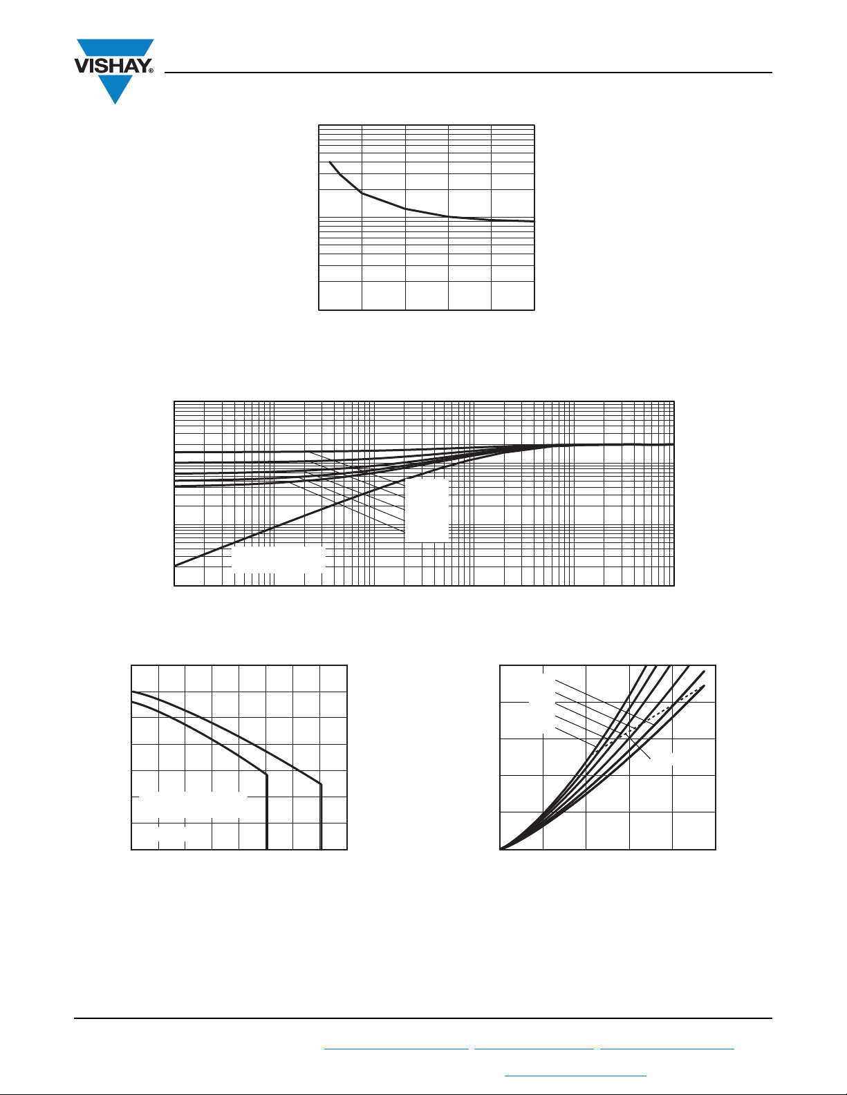
Fig. 3 - Typical Junction Capacitance vs. Reverse Voltage
Fig. 4 - Maximum Thermal Impedance Z
Fig. 5 - Maximum Allowable Case Temperature vs.
Revision: 10-Aug-11
For technical questions within your region: DiodesAmericas@vishay.com
THIS DOCUMENT IS SUBJECT TO CHANGE WITHOUT NOTICE. THE PRODUCTS DESCRIBED HEREIN AND THIS DOCUMENT
Average Forward Current
ARE SUBJECT TO SPECIFIC DISCLAIMERS, SET FORTH AT www.vishay.com/doc?91000
Characteristics
thJC
Fig. 6 - Forward Power Loss Characteristics
3
Document Number: 94647
, DiodesAsia@vishay.com, DiodesEurope@vishay.com
 Loading...