

PRODUCT SUMMARY
2N7000/2N7002, VQ1000J/P, BS170
Vishay Siliconix
N-Channel 60-V (D-S) MOSFET
Part Number V
2N7000
2N7002 7.5 @ VGS = 10 V 1 to 2.5 0.115
VQ1000J
VQ1000P 5.5 @ VGS = 10 V 0.8 to 2.5 0.225
BS170 5 @ VGS = 10 V 0.8 to 3 0.5
(BR)DSS
Min (V)
60
V
r
Max (W)
DS(on)
5 @ VGS = 10 V 0.8 to 3 0.2
5.5 @ VGS = 10 V 0.8 to 2.5 0.225
(V) ID (A)
GS(th)
FEATURES BENEFITS APPLICATIONS
D Low On-Resistance: 2.5 W
D Low Threshold: 2.1 V
D Low Input Capacitance: 22 pF
D Fast Switching Speed: 7 ns
D Low Input and Output Leakage
TO-226AA
(TO-92)
S
G
D
1
2
3
Top View
2N7000
Dual-In-Line
D Low Offset Voltage
D Low-Voltage Operation
D Easily Driven Without Buffer
D High-Speed Circuits
D Low Error Voltage
D Direct Logic-Level Interface: TTL/CMOS
D Drivers: Relays, Solenoids, Lamps, Hammers,
Displays, Memories, Transistors, etc.
D Battery Operated Systems
D Solid-State Relays
TO-236
(SOT-23)
G
1
S
2
Top View
Marking Code: 72wll
72 = Part Number Code for 2N7002
w = Week Code
ll = Lot Traceability
D
3
D
1
N
N
Document Number: 70226
S-04279—Rev. F, 16-Jul-01
S
1
G
1
NC NC
G
2
S
2
D
2
1
2
3
4
5
6
7
Top View
Plastic: VQ1000J
Sidebraze: VQ1000P
D
4
14
S
13
G
12
11
G
10
S
9
D
8
N
4
4
3
3
N
3
TO-92-18RM
(TO-18 Lead Form)
D
G
S
1
2
3
Top View
BS170
www.vishay.com
11-1
2N7000/2N7002, VQ1000J/P, BS170
Vishay Siliconix
ABSOLUTE MAXIMUM RATINGS (TA = 25_C UNLESS OTHERWISE NOTED)
Single Total Quad
Parameter Symbol 2N7000 2N7002
Drain-Source Voltage V
Gate-Source Voltage—Non-Repetitive V
Gate-Source Voltage—Continuous V
Continuous Drain Current
Continuous Drain Current
(T
= 150_C)
J
Pulsed Drain Current
Power Dissipation
Thermal Resistance, Junction-to-Ambient R
Operating Junction and
Storage Temperature Range
Notes
a. Pulse width limited by maximum junction temperature.
b. t
v 50 ms.
p
a
TA= 25_C
TA= 100_C
TA= 25_C
TA= 100_C
GSM
I
P
TJ, T
DS
GS
I
D
DM
thJA
60 60 60 60 60
"40 "40 "30 "25
"20 "20 "20 "20 "20
0.2 0.115 0.225 0.225 0.5
0.13 0.073 0.14 0.14 0.175
0.5 0.8 1 1
D
stg
0.4 0.2 1.3 1.3 2 0.83
0.16 0.08 0.52 0.52 0.8
312.5 625 96 96 62.5 156
VQ1000J VQ1000P
–55 to 150
SPECIFICATIONSĊ2N7000 AND 2N7002 (TA = 25_C UNLESS OTHERWISE NOTED)
Parameter Symbol Test Conditions TypaMin Max Min Max Unit
Static
Drain-Source Breakdown Voltage V
Gate-Threshold Voltage V
Gate-Body Leakage I
Zero Gate Voltage Drain Current I
On-State Drain Current
Drain-Source On-Resistance
Forward Transconductance
Common Source Output Conductance
b
b
b
b
(BR)DSS
r
Dynamic
Input Capacitance C
Output Capacitance C
Reverse Transfer Capacitance C
GS(th)
GSS
DSS
I
D(on)
DS(on)
DS(on)
g
fs
g
os
iss
oss
rss
VGS = 0 V, ID = 10 mA
VDS = VGS, ID = 1 mA 2.1 0.8 3
VDS = VGS, ID = 0.25 mA 2.0 1 2.5
VDS = 0 V, VGS = "15 V "10
VDS = 0 V, VGS = "20 V "100
VDS = 48 V, VGS = 0 V 1
TC = 125_C
VDS = 60 V, VGS = 0 V 1
TC = 125_C
VDS = 10 V, VGS = 4.5 V 0.35 0.075
VDS = 7.5 V, VGS = 10 V 1 0.5
VGS = 4.5 V, ID = 0.075 A 4.5 5.3
VGS = 5 V, ID = 0.05 A 3.2 7.5
TC = 125_C
VGS = 10 V, ID = 0.5 A 2.4 5 7.5
TJ = 125_C
VDS = 10 V, ID = 0.2 A 100 80
VDS = 5 V, ID = 0.05 A 0.5
VDS = 25 V, VGS = 0 V
f = 1 MHz
f = 1 MHz
70 60 60
5.8 13.5
4.4 9 13.5
22 60 50
11 25 25
2 5 5
VQ1000J/P
Limits
2N7000 2N7002
1000
BS170 Unit
V
A
W
_C/W
_C
V
nA
mA
500
A
W
mS
pF
www.vishay.com
11-2
Document Number: 70226
S-04279—Rev. F, 16-Jul-01
2N7000/2N7002, VQ1000J/P, BS170
W
W
m
W
W
Vishay Siliconix
SPECIFICATIONSĊ2N7000 AND 2N7002 (TA = 25_C UNLESS OTHERWISE NOTED)
Limits
2N7000 2N7002
Parameter Symbol Test Conditions TypaMin Max Min Max Unit
Switching
Turn-On Time t
Turn-Off Time t
Turn-On Time t
Turn-Off Time t
SPECIFICATIONSĊVQ1000J/P AND BS170 (TA = 25_C UNLESS OTHERWISE NOTED)
Static
Drain-Source Breakdown Voltage V
Gate-Threshold Voltage V
Gate-Body Leakage I
Zero Gate Voltage Drain Current I
On-State Drain Current
Drain-Source On-Resistance
Forward Transconductance
Common Source Output Conductance
Dynamic
Input Capacitance C
Output Capacitance C
Reverse Transfer Capacitance C
Switching
Turn-On Time t
Turn-Off Time t
Turn-On Time t
Turn-Off Time t
d
ON
OFF
ON
OFF
VDD = 15 V, RL = 25 W
VDD = 15 V, RL = 25
ID ^0.5 A, V
ID ^ 0.2 A, V
GEN
VDD = 30 V, RL = 150 W
VDD = 30 V, RL = 150
GEN
= 10 V, RG = 25 W
= 10 V, RG = 25 W
7 10
7 10
7 20
11 20
Limits
VQ1000J/P BS170
Parameter Symbol Test Conditions TypaMin Max Min Max Unit
(BR)DSS
GS(th)
GSS
GSS
DSS
DSS
b
b
b
b
I
D(on)
r
DS(on)
g
g
fs
os
iss
oss
rss
VGS = 0 V, ID = 100 mA
VDS = VGS, ID = 1 mA 2.1 0.8 2.5 0.8 3
VDS = 0 V, VGS = "10 V "100
TJ = 125_C
VDS = 0 V, VGS = "15 V "10
VDS = 25 V, VGS = 0 V 0.5
VDS = 48 V, VGS = 0 V, TJ = 125_C
VDS = 60 V, VGS = 0 V 10
VDS = 10 V, VGS = 10 V 1 0.5 A
VGS = 5 V, ID = 0.2 A 4 7.5
VGS = 10 V, ID = 0.2 A 2.3 5
VGS = 10 V, ID = 0.3 A 2.3 5.5
TJ = 125_C
VDS = 10 V, ID = 0.2 A 100
VDS = 10 V, ID = 0.5 A 100
VDS =5 V, ID = 0.05 A 0.5
VDS =25 V, VGS = 0 V
f = 1 MHz
f = 1 MHz
d
ON
OFF
ON
OFF
VDD = 15 V, RL = 23 W
VDD = 15 V, RL = 23
ID ^ 0.6 A, V
ID ^ 0.2 A, V
GEN
VDD = 25 V, RL = 125 W
VDD = 25 V, RL = 125
GEN
= 10 V, RG = 25 W
= 10 V, RG = 25 W
70 60 60
"500
500
4.2 7.6
22 60 60
11 25
2 5
7 10
7 10
7 10
7 10
ns
V
nA
mA
W
mS
pF
ns
Notes
a. For DESIGN AID ONLY, not subject to production testing. VNBF06
b. Pulse test: PW v80 ms duty cycle v1%.
c. This parameter not registered with JEDEC.
d. Switching time is essentially independent of operating temperature.
Document Number: 70226
S-04279—Rev. F, 16-Jul-01
www.vishay.com
11-3
2N7000/2N7002, VQ1000J/P, BS170
Vishay Siliconix
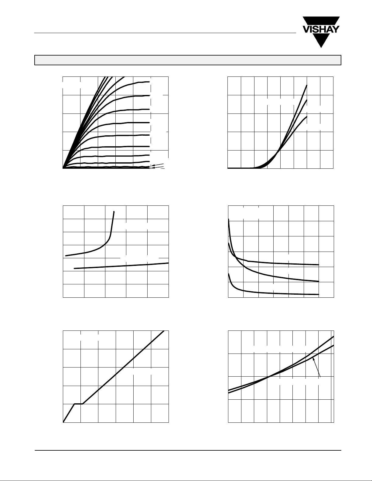
TYPICAL CHARACTERISTICS (TA = 25_C UNLESS OTHERWISE NOTED)
1.0
Output Characteristics Transfer Characteristics
VGS = 10, 9, 8, 7 V
0.8
0.6
0.4
– Drain Current (A)
D
I
0.2
0.0
0123456
VDS – Drain-to-Source Voltage (V)
7
6
5
4
3
– On-Resistance ( Ω )
2
DS(on)
r
1
0
0.0 0.2 0.4 0.6 0.8 1.0
I
– Drain Current (A)
D
rDS @ 5 V = V
rDS @ 10 V = V
6.5 V
6 V
5.5 V
5 V
4.5 V
4 V
3.5 V
3 V 2.5 V
GS
GS
2, 1 V
1.0
0.8
TJ = –55_C
0.6
0.4
– Drain Current (A)
D
I
0.2
0.0
012345678
– Gate-to-Source Voltage (V)
V
GS
CapacitanceOn-Resistance vs. Drain Current
60
VGS = 0 V
f = 1 MHz
50
40
30
20
C – Capacitance (pF)
10
0
0 5 10 15 20 25 30 35
– Drain-to-Source Voltage (V)
V
DS
C
iss
C
oss
C
rss
25_C
125_C
20
16
12
8
4
– Gate-to-Source Voltage (V)
GS
V
0
www.vishay.com
11-4
Gate Charge
ID = 0.5 A
VDS = 30 V
0 400 800 1200 1600 2000 2400
Qg – Total Gate Charge (pC)
(Normalized)
– On-Resistance ( Ω )
DS(on)
r
On-Resistance vs. Junction Temperature
2.0
VGS = 10 V, rDS @ 0.5 A
1.5
1.0
VGS = 5 V, rDS @ 0.05 A
0.5
0.0
–55 –30 –5 20 45 70 95 120 145
T
– Junction Temperature (_C)
J
Document Number: 70226
S-04279—Rev. F, 16-Jul-01

2N7000/2N7002, VQ1000J/P, BS170
TYPICAL CHARACTERISTICS (TA = 25_C UNLESS OTHERWISE NOTED)
Vishay Siliconix
1.000
Source-Drain Diode Forward Voltage On-Resistance vs. Gate-to-Source Voltage
TJ = 125_C
0.100
T
= 25_C
J
0.010
– Source Current (A)
S
I
0.001
0.0 0.2 0.4 0.6 0.8 1.0 1.2 1.4
VSD – Source-to-Drain Voltage (V) VGS – Gate-to-Source Voltage (V)
0.50
0.25
–0.00
– On-Resistance ( Ω )
DS(on)
r
Threshold Voltage
ID = 250 mA
6
I
5
4
= 50 mA
D
500 mA
3
2
1
0
0 2 4 6 8 101214161820
– Variance (V)
–0.25
GS(th)
V
–0.50
–0.75
–50 –25 0 25 50 75 100 125 150
Normalized Effective Transient Thermal Impedance, Junction-to-Ambient (TO-226AA, BS170 Only)
1
Duty Cycle = 0.5
0.2
0.1
0.05
0.1
0.02
Thermal Impedance
Normalized Effective Transient
0.01
0.1 1 10010 1 K
0.01
Single Pulse
t1 – Square Wave Pulse Duration (sec)
Notes:
P
DM
t
1
t
1. Duty Cycle, D =
2. Per Unit Base = R
3. TJM – TA = PDMZ
2
thJA
t
t
thJA
1
2
(t)
= 156_C/W
10 K
Document Number: 70226
S-04279—Rev. F, 16-Jul-01
www.vishay.com
11-5
 Loading...