

Page 1
PRODUCT SUMMARY
240
4.87
V
TN2404K/TN2404KL/BS107KL
Vishay Siliconix
N-Channel 240 -V (D-S) MOSFET
Part Number VDS Min (V)
TN2404K
TN2404KL/BS107KL
r
(W)
DS(on)
4 @ VGS = 10 V 0.8 to 2.0 0.2
4 @ VGS = 10 V 0.8 to 2.0 0.3
V
(V) ID (A) Qg (Typ)
GS(th)
FEATURES BENEFITS APPLICATIONS
D Low On-Resistance: 4 W
D Secondary Breakdown Free: 260 V
D Low Power/Voltage Driven
D Low Input and Output Leakage
D Excellent Thermal Stability
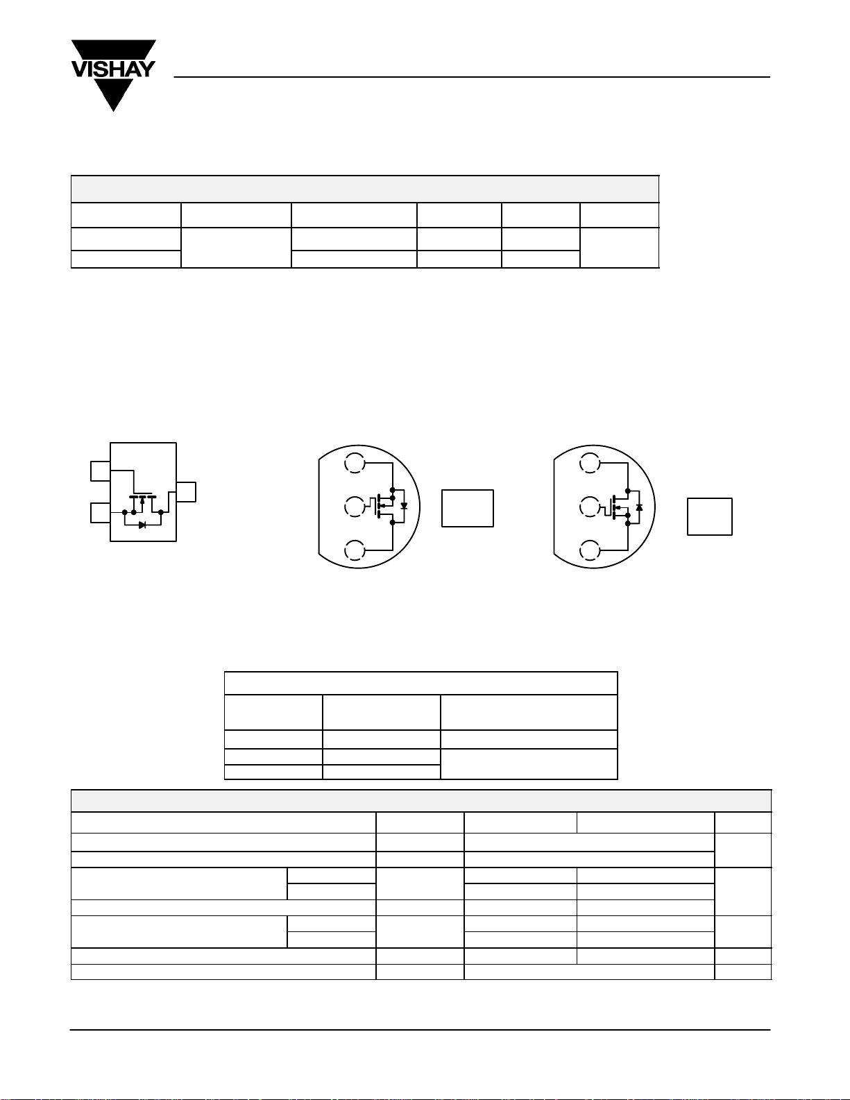
TO-236
(SOT-23)
G
1
D
3
S
2
Top View
TN2404K
Marking Code: K1ywl
K1 = Part Number Code for TN2404K
y = Year Code
w = Week Code
l = Lot Traceability
D Low Offset Voltage
D Full-Voltage Operation
D Easily Driven Without Buffer
D Low Error Voltage
D No High-Temperature
“Run-Away”
TO-226AA
(TO-92)
G
S
D
1
2
3
Top View
TN2404KL
Device Marking
Front View
“S” TN
2404KL
xxyy
“S” = Siliconix Logo
xxyy = Date Code
D High-Voltage Drivers: Relays, Solenoids,
Lamps, Hammers, Displays,
Transistors, etc.
D Telephone Mute Switches, Ringer Circuits
D Power Supply, Converters
D Motor Control
TO-92-18RM
(TO-18 Lead Form)
D
G
S
1
2
3
Top View
BS107KL
Device Marking
Front View
“S” BS
107KL
xxyy
“S” = Siliconix Logo
xxyy = Date Code
ABSOLUTE MAXIMUM RATINGS (TA = 25_C UNLESS OTHERWISE NOTED)
Parameter Symbol TN2404K TN2404KL/BS107KL Unit
Drain-Source Voltage V
Gate-Source Voltage V
Continuous Drain Current (TJ = 150_C)
Pulsed Drain Current
Power Dissipation
Thermal Resistance, Junction-to-Ambient R
Operating Junction and Storage Temperature Range TJ, T
Notes
a. Pulse width limited by maximum junction temperature.
b. Surface mounted on an FR4 board.
Document Number: 72225
S-41761—Rev. B , 04-Oct-04
a
ORDERING INFORMATION
Standard
Part Number
TN2404K-T1 TN2404K-T1—E3 With Tape and Reel Folding Option
TN2404KL-TR1 TN2404KL-TR1—E3
BS107KL-TR1 BS107KL-TR1—E3
_
TA= 25_C
TA= 70_C
TA= 25_C
TA= 70_C
Lead (Pb)-Free
Part Number
I
P
DS
GS
I
D
DM
D
thJA
stg
Spool Option
Option
"20
0.2 0.3
0.16 0.25
0.8 1.4
0.36 0.8
0.23 0.51
b
350
−55 to 150
240
156
A
W
_C/W
_C
www.vishay.com
1
Page 2
TN2404K/TN2404KL/BS107KL
b
()
VDD = 60 V, RL = 200 W
S
t
Off Ti
Vishay Siliconix
SPECIFICATIONS (TA = 25_C UNLESS OTHERWISE NOTED)
Parameter Symbol Test Conditions Min Typ
Static
Limits
a
Max Unit
Drain-Source Breakdown Voltage V
Gate-Threshold Voltage V
Gate-Body Leakage I
Zero Gate Voltage Drain Current I
On-State Drain Current
Drain-Source On-Resistance
Forward Transconductance
Diode Forward Voltage V
Dynamic
Total Gate Charge Q
Gate-Source Charge Q
Gate-Drain Charge Q
Turn-On Time
urn-
Notes
a. For DESIGN AID ONLY, not subject to production testing.
b. Pulse test: PW v300 ms duty cycle v2%.
Stresses beyond those listed under “Absolute Maximum Ratings” may cause permanent damage to the device. These are stress ratings only , and functional operation
of the device at these or any other conditions beyond those indicated in the operational sections of the specifications is not implied. Exposure to absolute maximum
rating conditions for extended periods may affect device reliability .
a
-
me
b
b
(BR)DSS
GS(th)
GSS
DSS
I
D(on)
r
DS(on)
g
fs
SD
g
gs
gd
t
d(on)
t
r
t
d(off)
t
r
VGS = 0 V, ID = 100 mA
VDS = VGS, ID = 250 mA
VDS = 0 V, VGS = "20 V "100 nA
VDS = 192 V, VGS = 0 V 1
TJ = 55_C
VDS = 10 V, VGS =10 V 0.8
VDS = 10 V, VGS = 4.5 V 0.5
VGS = 10 V, ID = 0.3 A 2.2 4
VGS = 4.5 V, ID = 0.2 A 2.3 4
VGS = 2.5 V, ID = 0.1 A 2.4 6
VDS = 10 V, ID = 0.3 A 1.6 S
IS = 0.3 A, VGS = 0 V 0.8 1.2 V
VDS = 192 V, VGS = 10 V, ID = 0.5 A
VDD = 60 V, RL = 200 W
ID ] 0.3 A, V
= 10 V, RG = 25 W
GEN
240 257
0.8 1.65 2.0
4.87 8
0.56
1.53
5 10
12 20
35 60
16 25
V
10
mA
A
W
nC
n
www.vishay.com
2
Document Number: 72225
S-41761—Rev. B , 04-Oct-04
Page 3

TN2404K/TN2404KL/BS107KL
TYPICAL CHARACTERISTICS (25_C UNLESS NOTED)
Vishay Siliconix
Output Characteristics Transfer Characteristics
1.8
VGS = 10 thru 3 V
1.5
1.2
0.9
0.6
− Drain Current (A)I
D
0.3
0.0
012345
VDS − Drain-to-Source Voltage (V)
On-Resistance vs. Drain Current
5
W )
4
3
− On-Resistance (r
2
DS(on)
1
0
0.0 0.2 0.4 0.6 0.8 1.0 1.2
VGS = 4.5 V
2.5 V
2 V
VGS = 10 V
1.4
1.2
1.0
0.8
0.6
− Drain Current (A)I
0.4
D
0.2
0.0
0123456
TC = −55_C
VGS − Gate-to-Source Voltage (V)
25_C
125_C
Capacitance
300
250
200
150
C − Capacitance (pF)
100
50
0
0 1020304050
C
iss
C
rss
C
oss
10
VDS = 192 V
= 0.5 A
I
D
8
6
4
− Gate-to-Source Voltage (V)
GS
2
V
0
012345
Document Number: 72225
S-41761—Rev. B , 04-Oct-04
− Drain Current (A)
I
D
Gate Charge
Qg − Total Gate Charge (nC)
VDS − Drain-to-Source Voltage (V)
On-Resistance vs. Junction Temperature
2.2
2.0
1.8
1.6
1.4
1.2
− On-Resiistance
(Normalized)
1.0
DS(on)
r
0.8
0.6
0.4
−50 −25 0 25 50 75 100 125 150
T
− Junction Temperature (_C)
J
VGS = 10 V
= 0.3 A
I
D
VGS = 4.5 V
= 0.2 A
I
D
www.vishay.com
3
Page 4

TN2404K/TN2404KL/BS107KL
Vishay Siliconix
TYPICAL CHARACTERISTICS (25_C UNLESS NOTED)
Source-Drain Diode Forward Voltage On-Resistance vs. Gate-to-Source Voltage
10
1
0.1
− Source Current (A)I
S
0.01
TJ = −55_C
TJ = 25_C
TJ = 150_C
W )
− On-Resistance (r
DS(on)
8
7
6
5
4
3
2
1
ID = 100 mA
ID = 50 mA
ID = 10 mA
0.001
0.0 0.2 0.4 0.6 0.8 1.0 1.2 1.4
VSD − Source-to-Drain Voltage (V) VGS − Gate-to-Source Voltage (V)
0.3
0.2
0.1
−0.0
−0.1
Variance (V)V
−0.2
GS(th)
−0.3
−0.4
−0.5
−50 −25 0 25 50 75 100 125 150
Normalized Thermal Transient Impedance, Junction-to-Ambient (TO-236, TN2404K Only)
2
0
0246810
Threshold Voltage
ID = 250 mA
TJ − Temperature (_C)
1
0.1
Thermal Impedance
Normalized Effective Transient
0.01
www.vishay.com
4
Duty Cycle = 0.5
0.2
0.1
0.05
0.02
−4
10
Single Pulse
−3
10
Notes:
P
DM
t
1
t
2
t
thJA
thJA
t
100
1
2
=350_C/W
(t)
1. Duty Cycle, D =
2. Per Unit Base = R
3. TJM − TA = PDMZ
4. Surface Mounted
−2
10
−1
1 10 60010
Square Wave Pulse Duration (sec)
Document Number: 72225
S-41761—Rev. B , 04-Oct-04
Page 5

TN2404K/TN2404KL/BS107KL
TYPICAL CHARACTERISTICS (25_C UNLESS NOTED)
Vishay Siliconix
1
Duty Cycle = 0.5
0.2
0.1
0.05
0.1
Thermal Impedance
Normalized Effective Transient
Single Pulse
0.01
0.1 1 10010 1 K
0.01
0.02
Normalized Effective Transient Thermal Impedance, Junction-to-Ambient
(TO-226AA, TN2404KL and TO-92-18RM, BS107KL Only)
Notes:
P
DM
t
1
1. Duty Cycle, D =
2. Per Unit Base = R
3. TJM − TA = PDMZ
t1 − Square Wave Pulse Duration (sec)
t
2
t
1
t
2
= 156_C/W
thJA
(t)
thJA
10 K
Vishay Siliconix maintains worldw ide manufacturing capability. Products may be manufactured at one of several qualified locations. Reliability data for Silicon Technology and
Package Reliability represent a composite of all qualified locations. For related documents such as package/tape drawings, part marking, and reliability data, see
http://www.vishay.com/ppg?72225.
Document Number: 72225
S-41761—Rev. B , 04-Oct-04
www.vishay.com
5
Page 6

Legal Disclaimer Notice
Vishay
Notice
Specifications of the products displayed herein are subject to change without notice. Vishay Intertechnology, Inc.,
or anyone on its behalf, assumes no responsibility or liability for any errors or inaccuracies.
Information contained herein is intended to provide a product description only. No license, express or implied, by
estoppel or otherwise, to any intellectual property rights is granted by this document. Except as provided in Vishay's
terms and conditions of sale for such products, Vishay assumes no liability whatsoever, and disclaims any express
or implied warranty, relating to sale and/or use of Vishay products including liability or warranties relating to fitness
for a particular purpose, merchantability, or infringement of any patent, copyright, or other intellectual property right.
The products shown herein are not designed for use in medical, life-saving, or life-sustaining applications.
Customers using or selling these products for use in such applications do so at their own risk and agree to fully
indemnify Vishay for any damages resulting from such improper use or sale.
Document Number: 91000 www.vishay.com
Revision: 08-Apr-05 1
 Loading...