

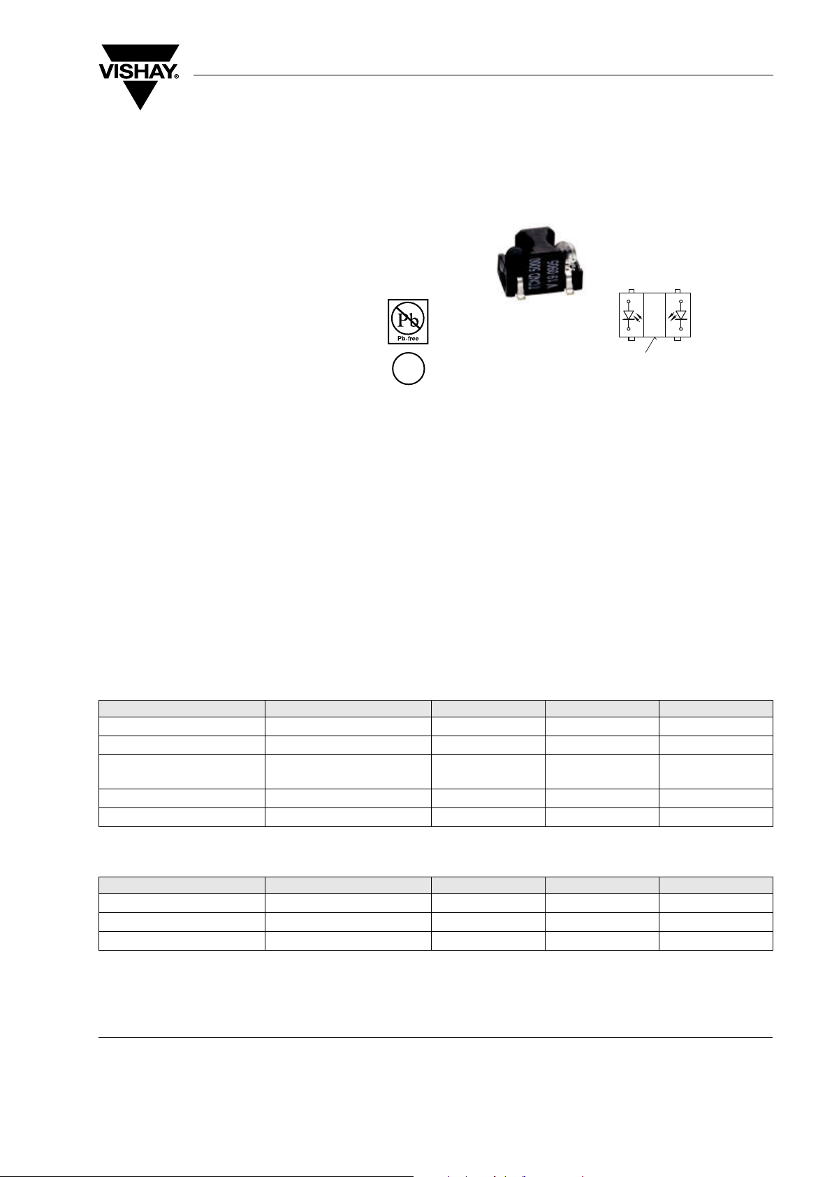
TCND5000
r
Vishay Semiconductors
Reflective Optical Sensor with PIN Photodiode Output
Description
The TCND5000 is a reflective sensor that includes an
infrared emitter and PIN photodiode in a surface
mount package which blocks visible light.
Features
• Package type: Surface mount
• Detector type: PIN Photodiode
• Dimensions:
L 6 mm x W 4.3 mm x H 3.75 mm
• Peak operating distance: 6 mm
• Peak operating range: 2 mm to 25 mm
• Typical output current under test: I
> 0.11 µA
ra
• Daylight blocking filter
• High linearity
• Emitter wavelength 940 nm
• Lead (Pb)-free soldering released
• Lead (Pb)-free component in accordance to RoHS
2002/95/EC and WEEE 2002/96/EC
• Minimum order quantity 2000 pcs, 2000 pcs/reel
e3
Detector
19967
Applications
• Proximity sensor
• Object sensor
• Motion sensor
• Touch key
Top view
A
C
Marking area
A
Emitte
C
Absolute Maximum Ratings
T
= 25 °C, unless otherwise specified
amb
Input (Emitter)
Parameter Test condition Symbol Val ue Unit
Reverse Voltage
Forward current
t
= 50 µs, T = 2 ms,
Peak Forward Current
Power Dissipation
Junction Temperature
p
T
amb
= 25 °C
Output (Detector)
Parameter Test condition Symbol Val ue Unit
Reverse Voltage
Power Dissipation
Junction Temperature
V
R
I
F
I
FM
P
V
T
j
V
R
P
V
T
j
5V
100 mA
500 mA
190 mW
100 °C
60 V
75 mW
100 °C
Document Number 83795
Rev. 1.2, 04-Sep-06
www.vishay.com
1
TCND5000
Vishay Semiconductors
Sensor
Paramete r Test condition Symbol Value Unit
Operating Temperature Range
Storage Temperature Range
Soldering Temperature acc. fig. 14
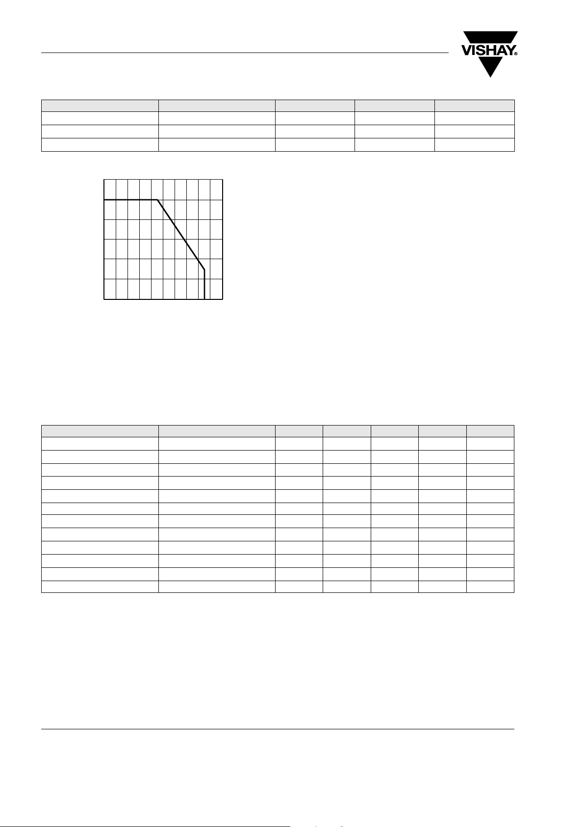
120
100
80
60
40
20
- Forward Current (mA)
F
I
0
20
0
10
16188
T
- Ambient Temperature (°C)
amb
Figure 1. Forward Current Limit vs. Ambient Temperature
50
30
40
70
60
100
90
80
T
amb
T
stg
T
sd
- 40 to + 85 °C
- 40 to + 100 °C
260 °C
Electrical Characteristics
T
= 25 °C, unless otherwise specified
amb
Input (Emitter)
Paramete r Test condition Symbol Min Ty p. Max Unit
= 20 mA, tp = 20 ms V
Forward Voltage
Temp. Coefficient of V
Reverse Current
Junction Capacitance
Radiant Intensity
F
I
F
IF = 1 mA TK
V
= 5 V I
R
= 0 V, f = 1 MHz, E = 0 C
V
R
I
= 20 mA, tp = 20 ms I
F
F
VF
R
j
e
Angle of Half Intensity ϕ ± 12 deg
Peak Wavelength
Spectral Bandwidth
Temp. Coefficient of λ
Rise Time
Fall Time
I
F
I
= 100 mA
F
p
IF = 100 mA TKλ
= 100 mA t
I
F
= 100 mA t
I
F
p
Δλ 50 nm
p
r
f
930 940 nm
= 100 mA λ
Virtual Source Diameter Method: 63 % encircled energy Ø 1.2 mm
see figures 2 to 8 accordingly
1.2 1.5 V
- 1.3 mV/K
10 µA
25 pF
775mW/sr
0.2 nm/K
800 ns
800 ns
www.vishay.com
2
Document Number 83795
Rev. 1.2, 04-Sep-06
TCND5000
Vishay Semiconductors
Output (Detector)
Parameter Test condition Symbol Min Ty p . Max Unit
= 50 mA V
Forward Voltage
Breakdown Voltage
Reverse Dark Current
Diode capacitance
Reverse Light Current
Temp. Coefficient of I
ra
Angle of Half Intensity ϕ ± 15 deg
Wavelength of Peak Sensitivity
Range of Spectral Bandwidth
see figures 9 to 12 accordingly
Sensor
T
= 25 °C, unless otherwise specified
amb
Parameter Test condition Symbol Min Ty p . Max Unit
Reverse Light Current V
I
F
= 100 µA V
I
R
= 10 V, E = 0 I
V
R
V
= 5 V, f = 1 MHz, E = 0 C
R
E
= 1 mW/cm
e
2
λ = 950 nm, VR = 5 V
VR = 5 V, λ = 870 nm TK
λ
= 2.5 V, IF = 20 mA
R
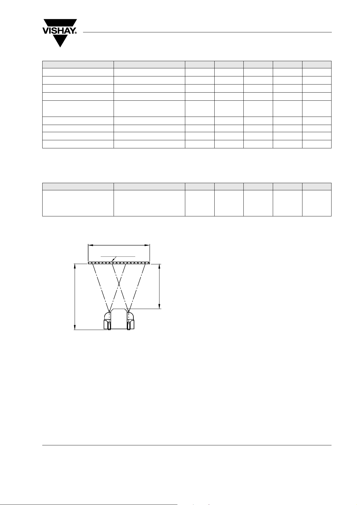
D = 30 mm
reflective mode:
see figure 2
F
BR
ro
D
I
ra
ira
λ
p
0.5
I
ra
60 V
110 nA
1.0 1.3 V
110nA
1.8 pF
12 µA
0.2 %/K
930 nm
840 to 1050 nm
D = 30 mm
30 mm
Kodak grey card
2 0 % Reflectivity
d = 26.25 mm
18223
Figure 2. Test Circuit
Document Number 83795
Rev. 1.2, 04-Sep-06
www.vishay.com
3

TCND5000
0°
10° 20°
Vishay Semiconductors
Typical Characteristics
T
= 25 °C, unless otherwise specified
amb
4
10
3
10
2
10
1
10
- Forward Current (mA)
F
I
0
10
0
13600
1
VF - Forward Voltage (V)
tP = 100 µs
t
/T = 0.001
P
3 2
4
Figure 3. Forward Current vs. Forward Voltage
1000
100
10
1
- Radiant Intensity (mW/sr)
e
I
16189
0.1
10
1
0
10
IF - Forward Current (mA)
10
3
2
10
4
10
Figure 4. Radiant Intensity vs. Forward Current
1.0
0.9
0.8
- Relative Intensity
e rel
0.7
I
0.6
18234
0.4
0.2
0
0.2
0.4
30°
40°
50°
60°
70°
80°
0.6
Figure 6. Relative Radiant Intensity vs. Angular Displacement
1000
100
10
- Reverse Dark Current (nA)
ro
I
1
20
94 8427
T
- Ambient Temperature (°C)
amb
VR = 10 V
806040
100
Figure 7. Reverse Dark Current vs. Ambient Temperature
1.25
1.0
0.75
0.5
- Relative Radiant Power
0.25
e rel
Φ
0
890
14291
Figure 5. Relative Radiant Power vs. Wavelength
IF = 100 mA
940
- Wavelength (nm)
λ
www.vishay.com
4
990
1.4
1.2
1.0
0.8
VR = 5 V
λ
= 950 nm
- Relative Reverse Light Current
ra, rel
0.6
I
94 8416
0
T
amb
4020
60
- Ambient Temperature (°C)
10080
Figure 8. Relative Reverse Light Current vs. Ambient Temperature
Document Number 83795
Rev. 1.2, 04-Sep-06

100
TCND5000
Vishay Semiconductors
0°
10° 20°
30°
10
V
= 5 V
CE
λ
= 950 nm
1
10
- Reverse Light Current (µA)
ra
I
16055
1.0
0.1
0.01
0.1
Ee - Irradiance (mW/cm²)
Figure 9. Reverse Light Current vs. Irradiance
8
6
E=0
f = 1 MHz
4
2
- Diode Capacitance (pF)
D
C
0
0.1
94 8430
1
10
VR- Reverse Voltage (V)
100
Figure 10. Diode Capacitance vs. Reverse Voltage
40°
50°
60°
70°
80°
0.6 0.4
- Relative Sensitivity
rel
S
94 8248
1.0
0.9
0.8
0.7
0.6
0.2 0.4
0.2
0
Figure 12. Relative Radiant Sensitivity vs. Angular Displacement
1.0
0.8
0.6
0.4
0.2
- Rel. Reverse Light Current
ra, rel
I
0.0
0
19966
5
d - Distance to Reflecting Card (mm)
Media: Kodak Gray Card
= 10 mA
I
F
10
40
45
3530252015
50
Figure 13. Relative Reverse Light Current vs. Distance
1.2
1.0
0.8
0.6
0.4
0.2
rel
λ
0
S ( ) - Relative Spectral Sensitivity
12786
750
850
950
λ - Wavelength (nm)
1050
Figure 11. Relative Spectral Sensitivity vs. Wavelength
Document Number 83795
Rev. 1.2, 04-Sep-06
1150
www.vishay.com
5

TCND5000
Vishay Semiconductors
Taping
www.vishay.com
6
18222
Document Number 83795
Rev. 1.2, 04-Sep-06

Package Dimensions in mm
TCND5000
Vishay Semiconductors
19968
Document Number 83795
Rev. 1.2, 04-Sep-06
www.vishay.com
7

TCND5000
Vishay Semiconductors
Precautions For Use
1. Over-current-proof
Customer must apply resistors for protection, otherwise slight voltage shift will cause big current change
(Burn out will happen).
2. Storage
2.1 Storage temperature and rel. humidity conditions
are: 5 °C to 30 °C, R.H. 60 %
2.2 Floor life must not exceed 72 h, acc. to JEDEC
level 4, J-STD-020.
Once the package is opened, the products should be
used within 72 h. Otherwise, they should be kept in a
damp proof box with desiccant.
Considering tape life, we suggest to use products
within one year from production date.
2.3 If opened more than 72 h in an atmosphere 5 °C
to 30 °C, R.H. 60 %, devices should be treated at
60 °C ± 5 °C for 15 hrs.
2.4 If humidity indicator in the package shows pink
color (normal blue), then devices should be treated
with the same conditions as 2.3
Reflow Solder Profiles
300
255 °C
250
240 °C
217 °C
200
150
100
Temperature (°C)
max. Ramp up 3°C/s max. Ramp down 6°C/s
50
0
0
Figure 14. Lead (Pb)-Free Reflow Solder Profile
300
max. 240 °C ca. 230 °C
250
200
150
100
Temperature (°C)
50
0
0
max. 120 s max. 100 s
50
Time (s)
215 °C
max. 160 °C
90s - 120s
2 K/s - 4 K/s
10050
Time (s)
max. 20 s
200
150100
10s
max 40s
Lead Temperature
full line : typical
dotted :process limits
150
19003
max. 260 °C
245 °C
250
948625
250200
300
www.vishay.com
8
Figure 15. Lead Tin (SnPb) Reflow Solder Profile
Document Number 83795
Rev. 1.2, 04-Sep-06

TCND5000
Vishay Semiconductors
Ozone Depleting Substances Policy Statement
It is the policy of Vishay Semiconductor GmbH to
1. Meet all present and future national and international statutory requirements.
2. Regularly and continuously improve the performance of our products, processes, distribution and operating
systems with respect to their impact on the health and safety of our employees and the public, as well as
their impact on the environment.
It is particular concern to control or eliminate releases of those substances into the atmosphere which are
known as ozone depleting substances (ODSs).
The Montreal Protocol (1987) and its London Amendments (1990) intend to severely restrict the use of ODSs
and forbid their use within the next ten years. Various national and international initiatives are pressing for an
earlier ban on these substances.
Vishay Semiconductor GmbH has been able to use its policy of continuous improvements to eliminate the use
of ODSs listed in the following documents.
1. Annex A, B and list of transitional substances of the Montreal Protocol and the London Amendments
respectively
2. Class I and II ozone depleting substances in the Clean Air Act Amendments of 1990 by the Environmental
Protection Agency (EPA) in the USA
3. Council Decision 88/540/EEC and 91/690/EEC Annex A, B and C (transitional substances) respectively.
Vishay Semiconductor GmbH can certify that our semiconductors are not manufactured with ozone depleting
substances and do not contain such substances.
We reserve the right to make changes to improve technical design
and may do so without further notice.
Parameters can vary in different applications. All operating parameters must be validated for each
customer application by the customer. Should the buyer use Vishay Semiconductors products for any
unintended or unauthorized application, the buyer shall indemnify Vishay Semiconductors against all
claims, costs, damages, and expenses, arising out of, directly or indirectly, any claim of personal
damage, injury or death associated with such unintended or unauthorized use.
Vishay Semiconductor GmbH, P.O.B. 3535, D-74025 Heilbronn, Germany
Document Number 83795
Rev. 1.2, 04-Sep-06
www.vishay.com
9

Legal Disclaimer Notice
Vishay
Document Number: 91000 www.vishay.com
Revision: 08-Apr-05 1
Notice
Specifications of the products displayed herein are subject to change without notice. Vishay Intertechnology, Inc.,
or anyone on its behalf, assumes no responsibility or liability for any errors or inaccuracies.
Information contained herein is intended to provide a product description only. No license, express or implied, by
estoppel or otherwise, to any intellectual property rights is granted by this document. Except as provided in Vishay's
terms and conditions of sale for such products, Vishay assumes no liability whatsoever, and disclaims any express
or implied warranty, relating to sale and/or use of Vishay products including liability or warranties relating to fitness
for a particular purpose, merchantability, or infringement of any patent, copyright, or other intellectual property right.
The products shown herein are not designed for use in medical, life-saving, or life-sustaining applications.
Customers using or selling these products for use in such applications do so at their own risk and agree to fully
indemnify Vishay for any damages resulting from such improper use or sale.
 Loading...