

Page 1
查询TCN75供应商
2-WIRE SERIAL TEMPERATURE
PRELIMINARY INFORMATION
SENSOR AND THERMAL MONIT OR
TCN75
TCN75
2-WIRE SERIAL TEMPERATURE SENSOR AND THERMAL MONITOR
FEATURES
■
Solid State Temperature Sensing; 2°C Accuracy (Typ.)
■ Operates from – 55°C to +125°C
■ Operating Range..................................... 2.7V - 5.5V
■ Programmable Trip Point and Hysteresis with
Power-up Defaults
■ Standard 2-Wire Serial Interface
■ Thermal Event Alarm Output Functions as
Interrupt or Comparator / Thermostat Output
■ Up to 8 TCN75's May Share the Same Bus
■ Shutdown Mode for Low Standby Power
Consumption
■ Low Power......................... 250µA (Typ.) Operating
1µA (Typ.) Shutdown Mode
■ 8-Pin Plastic DIP, SOIC, and MSOP Packaging
TYPICAL APPLICATIONS
■ Thermal Protection for High Performance CPU's
■ Solid-State Thermometer
■ Fire/Heat Alarms
■ Thermal Management in Electronic Systems:
Computers
Telecom Racks
Power Supplies / UPS* / Amplifiers
■ Copiers / Office Electronics
■ Consumer Electronics
■ Process Control
GENERAL DESCRIPTION
The TCN75 is a serially programmable temperature
sensor that notifies the host controller when ambient tem-
perature exceeds a user-programmed setpoint. Hysteresis
is also programmable. The INT/CMPTR output is programmable as either a simple comparator for thermostat operation or as a temperature event interrupt. Communication
with the TCN75 is accomplished via a two-wire bus that is
compatible with industry standard protocols. This permits
reading the current temperature, programming the setpoint
and hysteresis, and configuring the device.
The TCN75 powers up in Comparator Mode with a
default setpoint of 80°C with 5°C hysteresis. Defaults allow
independent operation as a stand-alone thermostat. A shutdown command may be sent via the 2-wire bus to activate
the low-power standby mode. Address selection inputs
allow up to eight TCN75's to share the same 2-wire bus for
multi-zone monitoring.
All registers can be read by the host and the INT/
CMPTR output's polarity is user programmable. Both polled
and interrupt driven systems are easily accommodated.
Small physical size, low installed cost, and ease of use make
the TCN75 an ideal choice for implementing sophisticated
system management schemes.
ORDERING INFORMATION
Supply Junction
Part No. Voltage (V) Package Temp. Range
TCN75-3.3MOA 3.3 8-Pin SOIC – 55°C to +125°C
TCN75-5.0MOA 5.0 8-Pin SOIC – 55°C to +125°C
T
CN75-3.3MPA 3.3 8-Pin PDIP – 55°C to +125°C
TCN75-5.0MPA 5.0 8-Pin PDIP – 55°C to +125°C
TCN75-3.3MUA 3.3 8-MSOP – 55°C to +125°C
TCN75-5.0MUA 5.0 8-MSOP – 55°C to +125°C
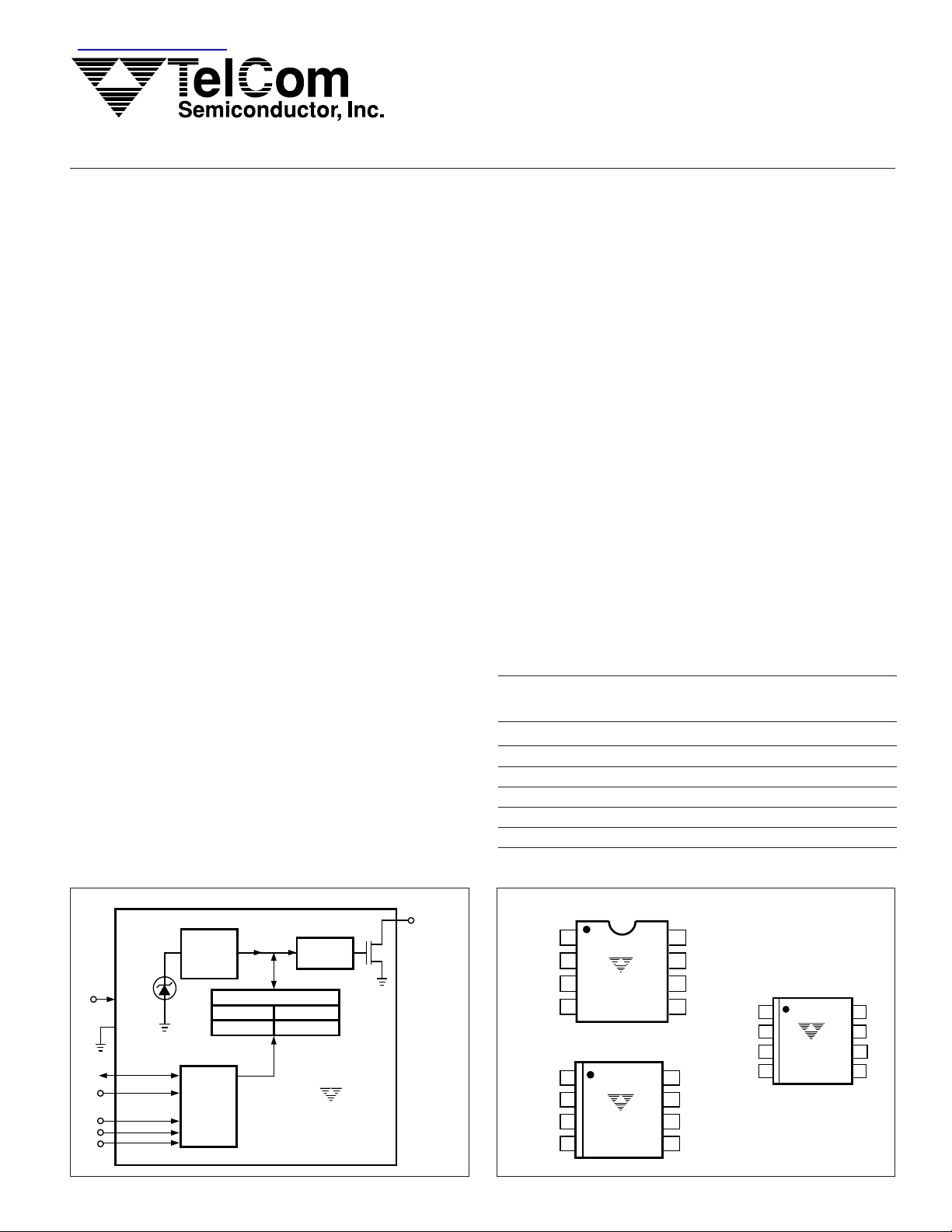
FUNCTIONAL BLOCK DIAGRAM
9 Bit
∆Σ
A/D
Temp
DD
SDA
SCL
Sensor
A
0
A
1
A
2
V
TCN75-04 6/16/97
Converter
Register Set
Configuration
Temperature
Two Wire
Serial Port
Interface
TelCom Semiconductor reserves the right to make changes in the circuitry and specifications of its devices.
T
T
Control
SET
HYST
Logic
TCN75
INT/CMPTR
PIN CONFIGURATIONS
8-Pin Plastic DIP
1
SDA V
2
SCL
INT/CMPTR A1
INT/CMPTR
1
GND
SDA
SCL
GND
3
TCN75MPA
4
8-Pin SOIC
1
2
TCN75MOA
3
4
8
7
6
5
8
7
6
5
DD
A0
A2
V
DD
A0
A1
A2
SDA
SCL
INT/CMPTR
GND
8-Pin MSOP
1
2
TCN75MUA
3
4
V
8
DD
7
A0
6
A1
5
A2
Page 2
PRELIMINARY INFORMATION
TCN75
2-WIRE SERIAL TEMPERATURE
SENSOR AND THERMAL MONIT OR
ABSOLUTE MAXIMUM RATINGS*
Supply Voltage (VDD) .................................................6.0V
ESD Susceptibility (Note 2)..................................... (TBD)
Voltage on Any Pin............. (GND – 0.3V) to (VDD + 0.3V)
Operating Temperature Range (TJ) ......– 55°C to +125°C
Storage Temperature Range (T
ELECTRICAL CHARACTERISTICS: V
) .....– 65°C to +150°C
STG
DD
= 2.7V – 5.5V, – 55°C ≤ (TA = TJ) ≤ 125°C, unless otherwise noted.
Lead Temperature (Soldering, 10 sec) ................. +300°C
Thermal Resistance (Junction to Ambient)
8-Pin DIP...................................................... 110°C/W
8-Pin SOIC .................................................. 170°C/W
8-Pin MSOP................................................ 250°C//W
*This is a stress rating only and functional operation of this device at these
or any other conditions above those indicated in the operations sections of
this specification is not implied.
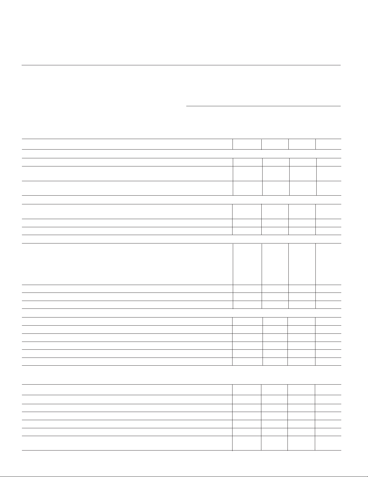
Symbol Parameter Test Conditions Min Typ Max Unit
Power Supply
V
I
I
DD
DD
DD1
Power Supply Voltage 2.7 — 5.5 V
Operating Current
Serial Port Inactive (T
= TJ = 25°C)
A
— 0.250 — mA
Serial Port Active — — 1.0
Standby Supply Current Shutdown Mode, Serial Port Inactive — 1 — µA
(TA = TJ = 25°C)
INT/CMPTR Output
I
OL
t
TRIP
V
OL
Sink Current: INT/CMPTR, SDA Note 1 — 1 4 mA
Outputs
INT/CMPTR Response Time User Programmable 1 — 6 t
CONV
Output Low Voltage IOL = 4.0mA — — 0.8 V
Temp-to-Bits Converter
∆T Temperature Accuracy (Note 2) – 55°C ≤ TA ≤ +125°C—±3—°C
V
= 3.3V : TCN75-3.3MOA,
DD
TCN75-3.3MPA, TCN75-3.3MUA
= 5.0V: TCN75-5.0MOA,
V
DD
TCN75-5.0MPA, TCN75-5.0 MUA
25°C ≤ TA ≤ 100°C—±0.5 ±2 °C
t
CONV
T
SET(PU)
T
HYST(PU)
Conversion Time — 100 — msec
TEMP Default Value Power Up — 80 — °C
T
Default Value Power Up — 75 — °C
HYST
2-Wire Serial Bus Interface
V
IH
V
IL
V
OL
C
IN
I
LEAK
I
OL(SDA)
Logic Input High VDD x 0.7 — — V
Logic Input Low — — VDD x 0.3 V
Logic Output Low IOL = 3mA — — 0.4 V
Input Capacitance SDA, SCL — 15 — pF
I/O Leakage
(TA = TJ = 25°C)
— ±100 — pA
SDA Output Low Current — — 6 mA
SERIAL PORT TIMING: 2.7V ≤ V
≤ 5.5V; – 55°C ≤ (TA = TJ ) ≤ 125°C, CL = 80pf, unless otherwise noted.
DD
Symbol Parameter Test Conditions Min Typ Max Unit
f
SC
t
LOW
t
HIGH
t
R
t
F
t
SU(START)
TCN75-04 6/16/97
Serial Port Frequency 0 100 400 kHz
Low Clock Period 1250 — — nsec
High Clock Period 1250 — — nsec
SCL and SDA Rise Time — — 250 nsec
SCL and SDA Fall Time — — 250 nsec
Start Condition Setup Time 1250 — — nsec
(for repeated Start Condition)
2
Page 3
2-WIRE SERIAL TEMPERATURE
SENSOR AND THERMAL MONIT OR
PRELIMINARY INFORMATION
TCN75
SERIAL PORT TIMING (Cont.): 2.7V ≤ V
≤ 5.5V; – 55°C ≤ (TA = TJ ) ≤ 125°C, CL = 80pf, unless otherwise
DD
noted.
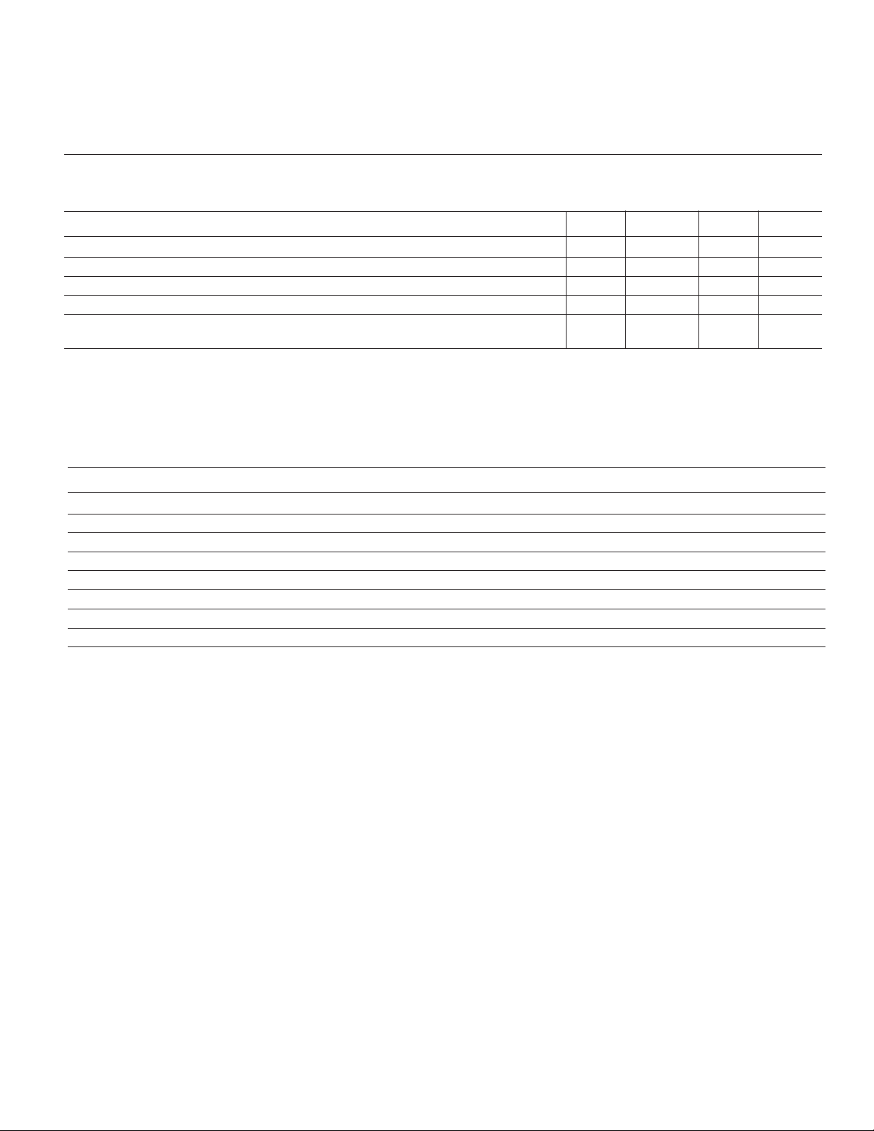
Symbol Parameter Test Conditions Min Typ Max Unit
t
H(START)
t
DSU
t
DH
t
SU(STOP)
t
IDLE
NOTES: 1. Output current should be minimized for best temperature accuracy. Power dissipation within the TCN75 will cause self-heating and
Start Condition Hold Time 1250 — — nsec
Data in Setup Time to SCL High 100 — — nsec
Data in Hold Time after SCL Low 0 — — nsec
Stop Condition Setup Time 1250 — — nsec
Bus Free Time Prior to New 1250 — — nsec
Transition
temperature drift. At maximum rated output current and saturation voltage, 4mA and 0.8V, respectively, the error amounts to 0.352°C for the
PDIP, and 0.544°C for the SOIC.
2. All part types of the TCN75 will operate properly over the wider power supply range of 2.7V to 5.5V. Each part type is tested and specified
for rated accuracy at its nominal supply voltage. As VDD varies from the nominal value, accuracy will degrade 1°C/V of VDD change.
3. Human body model, 100pF discharged through a 1.5k resistor, machine model, 200pF discharged directly into each pin.
PIN DESCRIPTION
Pin Number Symbol Description
1 SDA Bidirectional Serial Data.
2 SCL Serial Data Clock Input.
3 INT/CMPTR Interrupt or Comparator Output.
4 GND System Ground.
5A
6A
7A
8VDDPower Supply Input.
2
1
0
Address Select Pin (MSB).
Address Select Pin.
Address Select Pin (LSB).
DETAILED DESCRIPTION
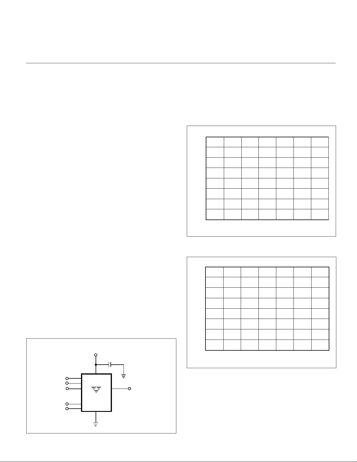
A typical TCN75 hardware connection is shown in
Figure 1.
Serial Data (SDA)
Bidirectional. Serial data is transferred in both directions
using this pin.
Serial Clock (SCL)
Input. Clocks data into and out of the TCN75.
INT/CMPTR
Open Collector, Programmable Polarity. In Comparator
Mode, unconditionally driven active any time temperature
exceeds the value programmed into the T
CMPTR will become inactive when temperature subsequently falls below the T
Programmer's Model.
setting. (See
HYST
) In Interrupt Mode, INT/CMPTR is
also made active by TEMP exceeding T
ally reset to its inactive state by reading any register via the
2-wire bus. If and when temperature falls below T
CMPTR is again driven active. Reading any register will
clear the T
TCN75-04 6/16/97
interrupt. In Interrupt Mode, the INT/CMPTR
HYST
register. INT/
SET
Register Set and
; it is uncondition-
SET
HYST
, INT/
output is unconditionally reset upon entering Shutdown
Mode. If programmed as an active-low output, it can be
wire-ORed with any number of other open collector devices.
Most systems will require a pull-up resistor for this configuration.
Note that current sourced from the pull-up resistor
causes power dissipation and may cause internal heating of
the TCN75. To avoid affecting the accuracy of ambient
temperature readings, the pull-up resistor should be made
as large as possible. INT/CMPTR's output polarity may be
programmed by writing to the INT/CMPTR POLARITY bit in
the CONFIG register. The default is active low.
Address (A2, A1, A0)
Inputs. Sets the three least significant bits of the TCN75
8-bit address. A match between the TCN75's address and
the address specified in the serial bit stream must be made
to initiate communication with the TCN75. Many protocolcompatible devices with other addresses may share the
same 2-wire bus.
Slave Address
The four most significant bits of the Address Byte (A6,
A5, A4, A3) are fixed to 1001[B]. The states of A2, A1 and
3
Page 4

PRELIMINARY INFORMATION
TCN75
2-WIRE SERIAL TEMPERATURE
SENSOR AND THERMAL MONIT OR
A0 in the serial bit stream must match the states of the A2,
A1 and A0 address inputs for the TCN75 to respond with an
Acknowledge (indicating the TCN75 is on the bus and ready
to accept data). The Slave Address is represented by:
TCN75 Slave Address
1001A2A1A0
MSB LSB
Comparator/Interrupt Modes
INT/CMPTR behaves differently depending on whether
the TCN75 is in Comparator Mode or Interrupt Mode.
Comparator Mode is designed for simple thermostatic operation. INT/CMPTR will go active anytime TEMP exceeds
T
. When in Comparator Mode, INT/CMPTR will remain
SET
active until TEMP falls below T
, whereupon it will reset
HYST
to its inactive state. The state of INT/CMPTR is maintained
in shutdown mode when the TCN75 is in comparator mode.
In Interrupt Mode, INT/CMPTR will remain active indefinitely, even if TEMP falls below T
, until any register is
HYST
read via the 2-wire bus. Interrupt Mode is better suited to
interrupt driven microprocessor-based systems. The INT/
CMPTR output may be wire-OR'ed with other interrupt
sources in such systems. Note that a pull-up resistor is
necessary on this pin since it is an open-drain output.
Entering Shutdown Mode will unconditionally reset INT/
CMPTR when in Interrupt Mode.
SHUTDOWN MODE
When the appropriate bit is set in the configuration
register (CONFIG) the TCN75 enters its low-power shutdown mode (IDD = 1µA, typical) and the temperature-todigital conversion process is halted. The TCN75's bus
interface remains active and TEMP, T
SET
, and T
HYST
may be
read from and written to. Transitions on SDA or SCL due to
external bus activity may increase the standby power consumption. If the TCN75 is in Interrupt Mode, the state of INT/
CMPTR will be RESET upon entering shutdown mode.
Fault Queue
To lessen the probability of spurious activation of INT/
CMPTR the TCN75 may be programmed to filter out transient events. This is done by programming the desired value
into the Fault Queue. Logic inside the TCN75 will prevent the
device from triggering INT/CMPTR unless the programmed
number of sequential temperature-to-digital conversions
yield the same qualitative result. In other words, the value
reported in TEMP must remain above T
for the consecutive number of cycles programmed in the
Fault Queue. Up to a six-cycle "filter" may be selected. See
Register Set and Programmer's Model
or below T
SET
.
HYST
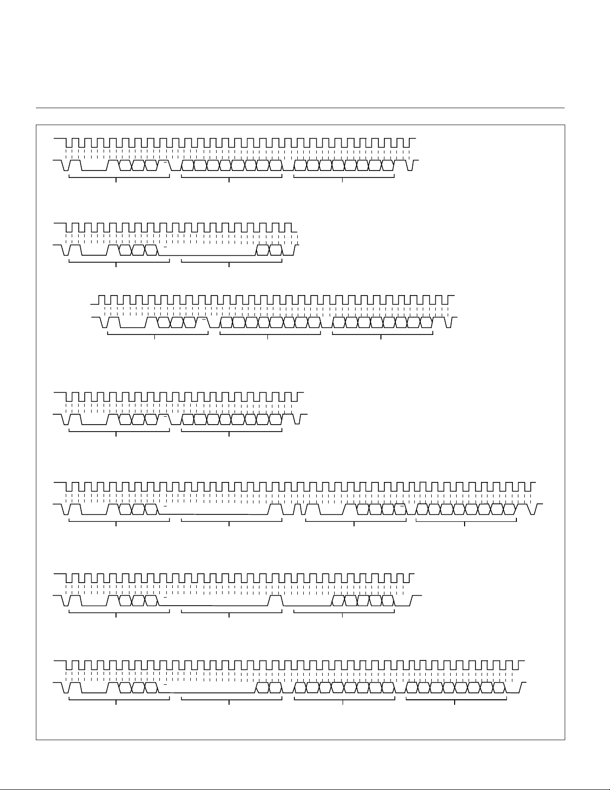
Serial Port Operation
The Serial Clock input (SCL) and bidirectional data port
(SDA) form a 2-wire bidirectional serial port for programming
and interrogating the TCN75. The following conventions are
used in this bus scheme:
TCN75 Serial Bus Conventions
Term Explanation
Transmitter The device sending data to the bus.
Receiver The device receiving data from the bus.
Master The device which controls the bus: initiating
transfers (START), generating the clock, and
terminating transfers (STOP).
Slave The device addressed by the master.
Start A unique condition signaling the beginning of a
transfer indicated by SDA falling (High-Low) while
SCL is high.
Stop A unique condition signaling the end of a transfer
indicated by SDA rising (Low - High) while SCL is
high.
ACK A Receiver acknowledges the receipt of each
byte with this unique condition. The Receiver
drives SDA low during SCL high of the ACK
clock-pulse. The Master provides the clock pulse
for the ACK cycle.
NOT Busy When the bus is idle, both SDA & SCL will
remain high.
Data Valid The state of SDA must remain stable during the
High period of SCL in order for a data bit to be
considered valid. SDA only changes state while
SCL is low during normal data transfers. (See
Start and Stop conditions)
All transfers take place under control of a host, usually
a CPU or microcontroller, acting as the Master, which
provides the clock signal for all transfers. The TCN75
operates as a Slave. This serial protocol is illustrated in
Figure 2. All data transfers have two phases; and all bytes
are transferred MSB first. Accesses are initiated by a start
condition (START), followed by a device address byte and
one or more data bytes. The device address byte includes
a Read/Write selection bit. Each access must be terminated
by a Stop Condition (STOP). A convention called
edge
(ACK) confirms receipt of each byte. Note that SDA
can change only during periods when SCL is LOW (SDA
changes while SCL is HIGH are reserved for Start and Stop
Conditions).
Start Condition (START)
The TCN75 continuously monitors the SDA and SCL
lines for a start condition (a HIGH to LOW transition of SDA
while SCL is HIGH), and will not respond until this condition
is met.
always
Acknowl-
TCN75-04 6/16/97
4
Page 5
2-WIRE SERIAL TEMPERATURE
SENSOR AND THERMAL MONIT OR
PRELIMINARY INFORMATION
TCN75
Address Byte
Immediately following the Start Condition, the host must
next transmit the address byte to the TCN75. The four most
significant bits of the Address Byte (A6, A5, A4, A3) are fixed
to 1001(B). The states of A2, A1 and A0 in the serial bit
stream must match the states of the A2, A1 and A0 address
inputs for the TCN75 to respond with an Acknowledge
(indicating the TCN75 is on the bus and ready to accept
data). The eighth bit in the Address Byte is a Read-Write Bit.
This bit is a 1 for a read operation or 0 for a write operation.
Acknowledge (ACK)
Acknowledge (ACK) provides a positive handshake
between the host and the TCN75. The host releases SDA
after transmitting eight bits then generates a ninth clock
cycle to allow the TCN75 to pull the SDA line LOW to
acknowledge that it successfully received the previous eight
bits of data or address.
Data Byte
After a successful ACK of the address byte, the host
must next transmit the data byte to be written or clock out the
data to be read. (See the appropriate timing diagrams.) ACK
will be generated after a successful write of a data byte into
the TCN75.
over the power supply voltage range of 2.7V to 5.5V, but
with a lower measurement accuracy. Figure 2 shows the
worst case temperature measurement error for the
TCN75CO_-3 operated at a power supply voltage of 5V ±
10%. Figure 3 shows the worst case temperature measurement error for the TCN75CO_-3 operated at a power supply
voltage of 3.3V ±10%.
±5
±4
±3
ERROR (°0)
±2
±1
20 35 50 65 80 12595 110
TCN75 Case Temeprature (°C)
Figure 2. TCN75CO_-3 Measurement Error at V
= 5V ± 10%
DD
Stop Condition (STOP)
Communications must be terminated by a stop condition (a LOW to HIGH transition of SDA while SCL is HIGH).
The Stop Condition must be communicated by the transmitter to the TCN75.
Power Supply
To minimize temperature measurement error, the
TCN75VO_-3 is factory calibrated at a supply voltage of
3.3V ±5V and the TCN75CO_-5 is factory calibrated at a
supply voltage of 5V ±5%. Either device is fully operational
(3V to 5.5V)
+V
DD
C
Address
(Set as Desired)
2
I
C Interface
A
SDA
SCL
Bypass
8
A
A
7
0
6
1
5
2
TCN75
1
2
4
0.1µF Recommended
Unless Device is Mounted
Close to CPU
3
INT/CMPTR
TO PROCESSOR
±5
±4
±3
ERROR (°0)
±2
±1
20 35 50 65 80 12595 110
TCN75 Case Temeprature (°C)
Figure 3. TCN75CO_-5 Measurement Error at V
= 3.3V ± 10%
DD
TCN75-04 6/16/97
Figure 1. Typical Application
5
Page 6
PRELIMINARY INFORMATION
TCN75
2-WIRE SERIAL TEMPERATURE
SENSOR AND THERMAL MONIT OR
1
00
1
Start
by
Master
Address Byte
(a) Typical 2-Byte Read From Preset Pointer Location Such as Temp, TOS, T
1
00
1
Start
by
Master
1 A2A1A0
Address Byte
1
00
1
Repeat
Start
by
Master
Address Byte
19199
D7 D6 D5 D4 D3 D2 D1 D0 D7 D6 D5 D4 D3 D2 D1 D01 A2A1A0
R/W
Ack
by
Most Significant Data Byte
TCN75
199
R/W
000000D1D0
Ack
by
TCN75
Pointer Byte
19199
D7 D6 D5 D4 D3 D2 D1 D0 D7 D6 D5 D4 D3 D2 D1 D01 A2A1A0
R/W
Ack
by
Most Significant Data Byte
TCN75
Ack
by
Least Significant Data Byte
Master
HYST
. . . . .
. . . . .
Ack
by
TCN75
Ack
Master
by
Least Significant Data Byte
(b) Typical Pointer Set Followed by Immediate Read for 2-Byte Register Such as Temp, TOS, T
1
00
1
Start
by
Master
Address Byte
199
D7 D6 D5 D4 D3 D2 D1 D01 A2A1A0
R/W
Ack
by
TCN75
Data Byte
No Ack
by
Master
Stop
Cond
by
Master
(c) Typical 1-Byte Read From Configuration Register With Preset Pointer
1
19199
HYST
Stop
No Ack
Cond
by
Master
by
Master
Stop
No Ack
Cond
by
Master
19
by
Master
0 0 0 0 0 0 0 D0 D7 D6 D5 D4 D3 D2 D1 D0100 A21A1A01 A2A1A0
00
1
Start
by
Master
Address Byte
(d) Typical Pointer Set Followed by Immediate Read from Configuration Register
1
00
1
Start
by
Master
Address Byte
R/W
Ack
R/W
by
TCN75
Ack
by
TCN75
Pointer Byte
19199
000000D1D0 00 0 D4 D2D3 D1 D01 A2A1A0
Pointer Byte
Ack
by
TCN75
Ack
by
TCN75
Repeat
Master
(e) Configuration Register Write
1
1
Start
by
Master
(f) TOS and T
00
Address Byte
HYST
Write
19199
000000D1D0 D7D6D5D4D3D2D1D0D6 D5 D4 D2D3 D1 D01 A2A1A0
R/W
Ack
by
TCN75
Pointer Byte
Ack
by
TCN75
Figure 2. Timing Diagrams
TCN75-04 6/16/97
Start
by
D7
Address Byte
Configuration Byte
Most Significant Data Byte
6
R/W
Stop
Ack
by
TCN75
No Ack
by
Master
Cond
Master
Stop
by
Cond
by
Master
Ack
by
TCN75
Stop
Ack
Cond
by
by
TCN75
Master
19
Ack
by
Least Significant Data Byte
TCN75
Data Byte
Page 7
2-WIRE SERIAL TEMPERATURE
SENSOR AND THERMAL MONIT OR
PRELIMINARY INFORMATION
TCN75
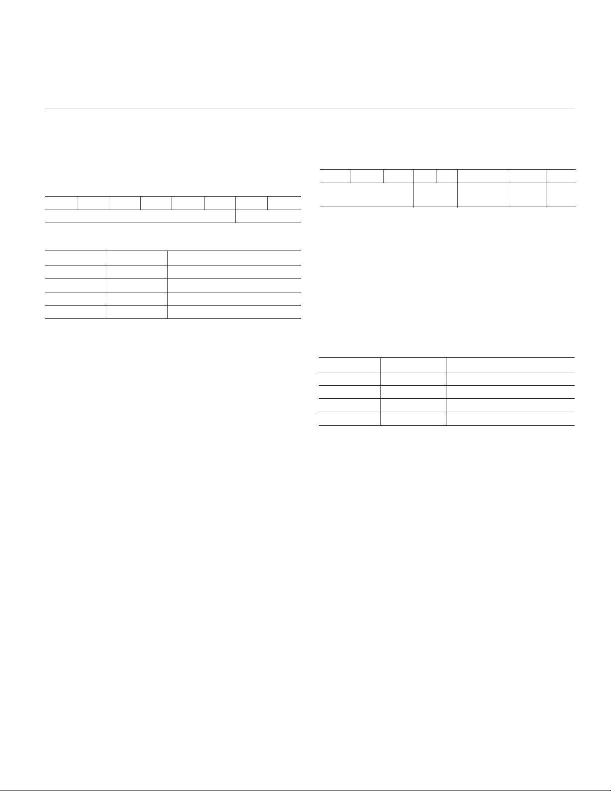
REGISTER SET AND PROGRAMMER'S MODEL
Register (POINT), 8-bits, Write-only
Pointer Register (POINT)
D[7] D[6] D[5] D[4] D[3] D[2] D[1] D[0]
Must Be Set To Zero Pointer
Register Selection via the Pointer Register:
D1 D0 Register Selection
0 0 TEMP
0 1 CONFIG
10T
11T
HYST
SET
Configuration Register (CONFIG), 8-bits,
Read/Write
Configuration Register (CONFIG)
D[7] D[6] D[5] D[4] D[3] D[2] D[1] D[0]
Must Be Set To Zero Fault INT/CMPTR. COMP/ Shut-
Queue POLARITY INT. Down
D0: Shutdown: 0 = Normal Operation
1 = Shutdown Mode
D1: CMPTR/INT: 0 = Comparator Mode
1 = Interrupt Mode
D2: INT/CMPTR POLARITY: 0 = Active Low
1 = Active High
D3 - D4: Fault Queue: Number of sequential temperature-
to-digital conversions with the same result before the
INT/CMPTR output is updated:
D4 D3 Number of Conversions
0 0 1 (Power-up-default)
012
104
116
TCN75-04 6/16/97
7
Page 8
PRELIMINARY INFORMATION
2-WIRE SERIAL TEMPERATURE
SENSOR AND THERMAL MONIT OR
TCN75
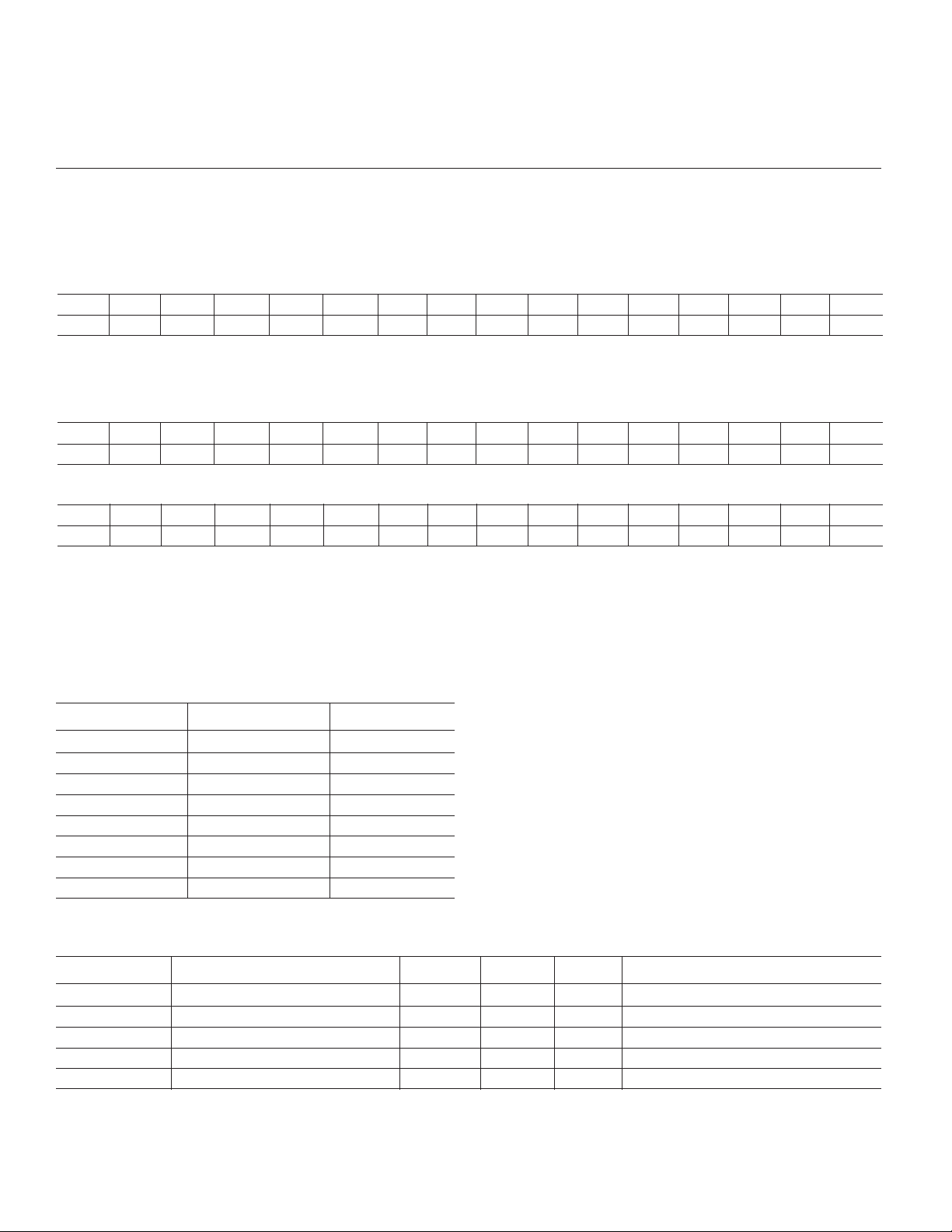
Temperature (TEMP) Register, 16-bits, Read-only
The binary value in this register represents ambient
temperature following a conversion cycle.
Temperature Register (TEMP)
D[15] D[14] D[13] D[12] D[11] D[10] D[9] D[8] D[7] D[6] D[5] D[4] D[3] D[2] D[1] D[0]
MSB D7 D6 D5 D4 D3 D2 D1 LSB X X X X X X X
Temperature Setpoint (T
Temperature Setpoint Register (T
D[15] D[14] D[13] D[12] D[11] D[10] D[9] D[8] D[7] D[6] D[5] D[4] D[3] D[2] D[1] D[0]
MSB D7 D6 D5 D4 D3 D2 D1 LSB X X X X X X X
Hysteresis Register (T
D[15] D[14] D[13] D[12] D[11] D[10] D[9] D[8] D[7] D[6] D[5] D[4] D[3] D[2] D[1] D[0]
MSB D7 D6 D5 D4 D3 D2 D1 LSB X X X X X X X
In the TEMP, T
SET
HYST
, and T
)
HYST
) and Hysteresis (T
SET
)
SET
registers, each unit value
) Register, 16-bits, Read-Write:
HYST
represents one-half degree (Celsius). The value is in 2's complement binary format such that a reading of 000000000b
corresponds to 0°C. Examples of this temperature to binary
value relationship are shown in the following table.
Temperature to Digital Value Conversion
Temperature Binary Value HEX Value
+125°C 0 11111010 0FA
+25°C 0 00110010 032
+0.5°C 0 00000001 001
0°C 0 00000000 00
– 0.5°C 1 11111111 1FF
– 25°C 1 11001110 1CE
– 40°C 1 10110000 1B0
– 55°C 1 10010010 192
The TCN75's register set is summarized below
Name Description Width Read Write Notes
TEMP Ambient Temperature 16 X 2's Complement Format
T
SET
T
HYST
POINT Register Pointer 8 X X
CONFIG Configuration Register 8 X X
TCN75-04 6/16/97
Temperature Setpoint 16 X X 2's Complement Format
Temperature Hysteresis 16 X X 2's Complement Format
8
Page 9
2-WIRE SERIAL TEMPERATURE
SENSOR AND THERMAL MONIT OR
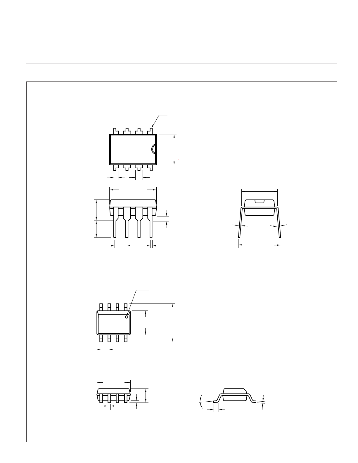
PACKAGE DIMENSIONS
PRELIMINARY INFORMATION
TCN75
8-Pin Plastic DIP
PIN 1
.260 (6.60)
.240 (6.10)
.045 (1.14)
.030 (0.76)
.200 (5.08)
.140 (3.56)
.150 (3.81)
.115 (2.92)
.400 (10.16)
.348 (8.84)
.110 (2.79)
.090 (2.29)
.070 (1.78)
.045 (1.14)
.022 (0.56)
.015 (0.38)
.157 (3.99)
.150 (3.81)
PIN 1
.244 (6.20)
.228 (5.79)
.040 (1.02)
.020 (0.51)
8-Pin SOIC
.015 (0.38)
.008 (0.20)
.310 (7.87)
.290 (7.37)
3°MIN.
.400 (10.16)
.310 (7.87)
TCN75-04 6/16/97
.050 (1.27) TYP.
.197 (5.00)
.189 (4.80)
.018 (0.46)
.014 (0.36)
.010 (0.25)
.004 (0.10)
.069 (1.75)
.053 (1.35)
8°MAX.
9
.010 (0.25)
.007 (0.18)
.050 (1.27)
.016 (0.40)
Dimensions: inches (mm)
Page 10
PRELIMINARY INFORMATION
TCN75
2-WIRE SERIAL TEMPERATURE
SENSOR AND THERMAL MONIT OR
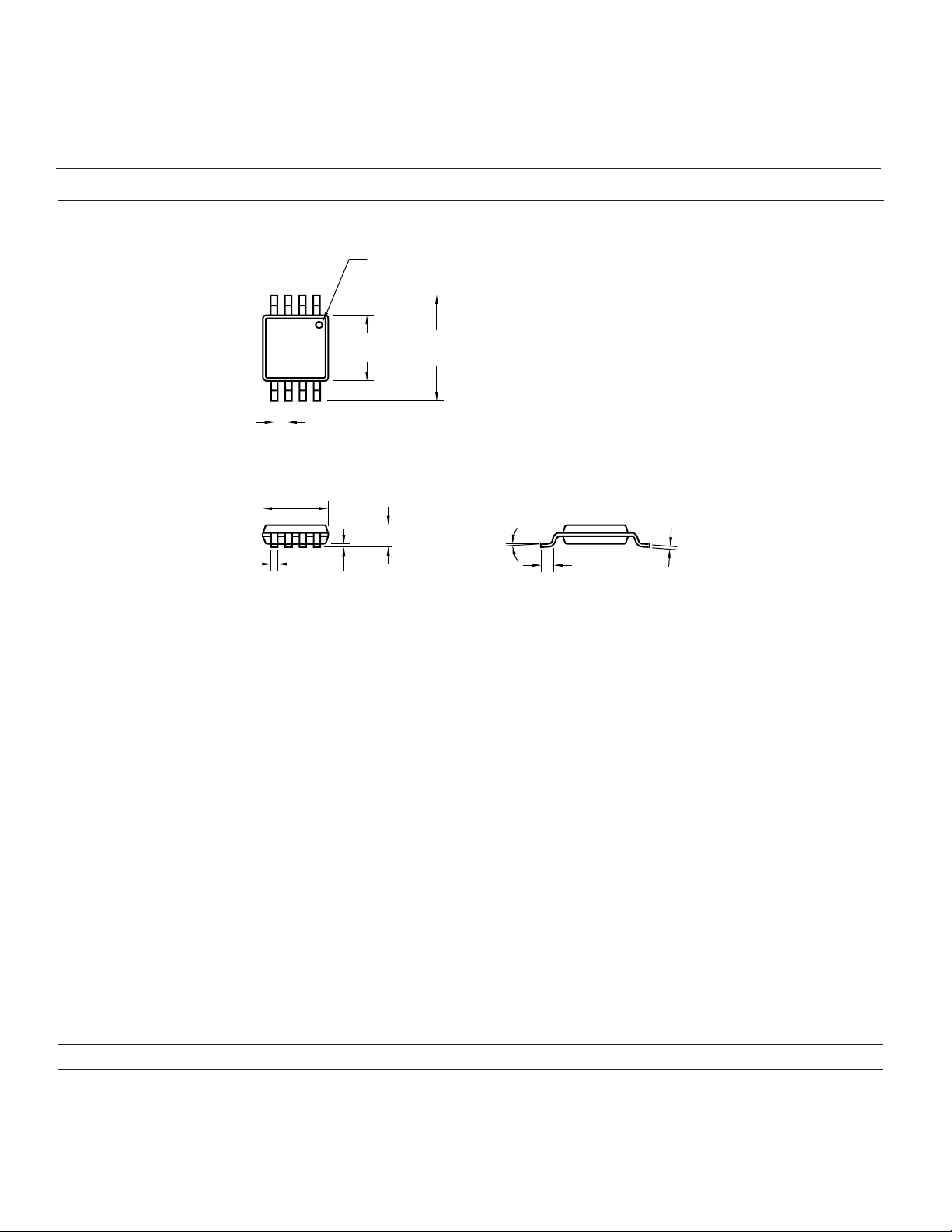
8-Pin MSOP
PIN 1
.026 (0.65) TYP.
.122 (3.10)
.114 (2.90)
.016 (0.40)
.010 (0.25)
.006 (0.15)
.002 (0.05)
.122 (3.10)
.114 (2.90)
.197 (5.00)
.187 (4.80)
.043 (1.10)
MAX.
6°MAX.
.008 (0.20)
.005 (0.13)
.028 (0.70)
.016 (0.40)
Dimensions: inches (mm)
Sales Offices
TelCom Semiconductor
1300 Terra Bella Avenue
P.O. Box 7267
Mountain View, CA 94039-7267
TEL: 415-968-9241
FAX: 415-967-1590
E-Mail: [email protected]
TCN75-04 6/16/97
TelCom Semiconductor
Austin Product Center
9101 Burnet Rd. Suite 214
Austin, TX 78758
TEL: 512-873-7100
FAX: 512-873-8236
10
TelCom Semiconductor H.K. Ltd.
10 Sam Chuk Street, Ground Floor
San Po Kong, Kowloon
Hong Kong
TEL: 852-2324-0122
FAX: 852-2354-9957
Printed in the U.S.A.
 Loading...