

Page 1
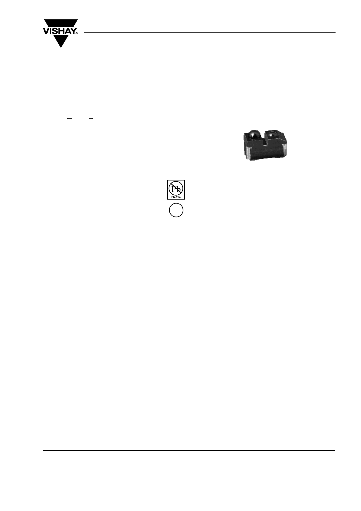
Reflective Sensor for Touchless Switch
Description
TCND3000 is a reflective optical sensor for applications using the HALIOS® (H
pendent O
infrared emitter and a photodetector forming the optical sensing path. According to the HALIOS principle a
second infrared emitter is used for compensation of
disturbing ambient light. Optoelectronic parameters of
the sensor are matched to the corresponding integrated circuit E909.01, manufactured by ELMOS
Semiconductor AG (www.elmos.de).
ptical System) principle. It consists of an
Features
• Package type: Surface mount
• Detector type: PIN Photodiode
• Dimensions:
L 4.83 mm x W 2.54 mm x H 2.21 mm
• Peak operating distance: 20 mm
• Peak operating range: 10 mm to 20 mm
• Typical output current under test: I
• Lead (Pb)-free soldering released
• Lead (Pb)-free component in accordance to RoHS
2002/95/EC and WEEE 2002/96/EC
• Emitter wavelength 885 nm
• Daylight blocking filter
• Touch distance: 10 mm*)
• Proximity distance: 20 mm*)
• High ambient light suppression for sunlight:
≤ 200 klx
• High ambient light suppression for CIE standard
illuminant A: ≤ 100 klx
• Minimum order quantity 800 pcs, 800 pcs/reel
*) Using E909.01 interface ASIC and Kodak grey card
with 20 % diffuse reflection
igh Ambient Light Inde-
e4
= 5.6 µA
C
Applications
• Optical switches for general purpose
TCND3000
Vishay Semiconductors
Document Number 84606
Rev. 1.2, 23-Aug-06
www.vishay.com
1
Page 2
TCND3000
R
thJA
Vishay Semiconductors
Absolute Maximum Ratings
T
= 25 °C, unless otherwise specified
amb
Sensor
Parameter Test condition Symbol Val ue Unit
≤ 25 °C P
Power dissipation
Storage temperature range
Operating temperature range
Thermal resistance
junction/ambient
Soldering temperature acc. figure 7
IR Emitter LEDS (Transmitter)
Parameter Test condition Symbol Val ue Unit
Reverse voltage
Forward current
Peak forward current
Junction temperature
T
amb
T
s
t
ps
= 8 µs
= 4 µs
V
T
stg
T
amb
R
thJA
T
sd
V
RS
I
FS
I
FS
T
js
180 mW
- 40 to + 100 °C
- 40 to + 85 °C
450 K/W
260 °C
5V
50 mA
100 mA
105 °C
IR Emitter LEDC (Compensation)
Parameter Test condition Symbol Val ue Unit
Reverse voltage
Forward current
= 8 µs
T
Peak forward current
s
t
pc
= 4 µs
Junction temperature
Detector
Parameter Test condition Symbol Val ue Unit
Reverse voltage
Junction temperature
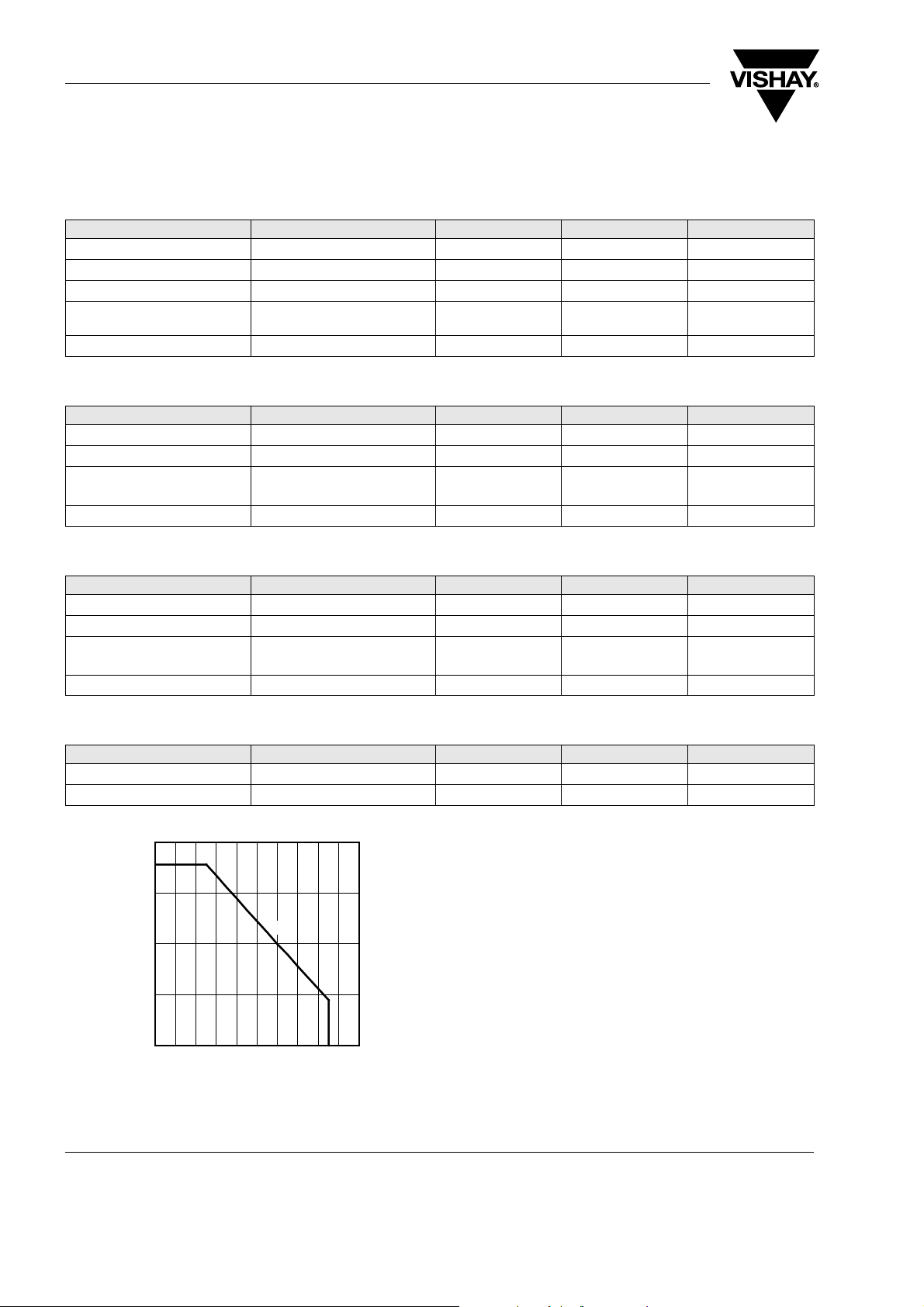
200
150
100
- Power Dissipation (mW)
V
50
P
V
RC
I
FC
I
FC
T
js
V
RD
T
jD
5V
50 mA
100 mA
105 °C
5V
105 °C
0
0
20
T
- Ambient Temperature (°C)
amb
100
806040
Figure 1. Power Dissipation Limit vs. Ambient Temperature
www.vishay.com
2
Document Number 84606
Rev. 1.2, 23-Aug-06
Page 3
TCND3000
Vishay Semiconductors
Electrical Characteristics
T
= 25 °C, unless otherwise specified
amb
Sensor
Parameter Test condition Symbol Min Ty p. Max Unit
Light current Kodak Grey Card
I
CA
20 % diffuse reflection
distance: 1 cm
I
= 10 mA
FS
Optical crosstalk sensing path no reflective medium
I
= 10 mA
FS
= 2 mA I
Compensation current
I
FC
I
CA
CR
IR Emitter LEDS (Transmitter)
Parameter Test condition Symbol Min Ty p. Max Unit
Forward voltage I
Reverse voltage
= 10 mA
FS
= 20 ms
t
p
I
= 10 µA V
RS
Junction capacitance C
Radiant intensity I
= 10 mA
FS
= 20 ms
t
p
Angle of half intensity
= 10 mA λ
Peak wavelength
Spectral bandwidth
I
FS
= 10 mA Δλ
I
FS
Virtual source diameter DIN EN ISO 1146/1:2005 Ø 1.4 mm
V
FS
RS
jS
I
e
ϕ
S
ps
s
5V
875 885 nm
1.2 µA
0.9 µA
5 µA
1.3 V
50 pF
222mW/sr
± 20 deg
42 nm
IR Emitter LEDC (Compensation)
Parameter Test condition Symbol Min Ty p. Max Unit
Forward voltage I
Reverse voltage
= 10 mA
FC
= 20 ms
t
pC
I
= 10 µA V
RC
Junction capacitance
= 10 mA λ
Peak wavelength
Spectral bandwidth
I
FC
= 10 mA Δλ
I
FC
Detector
Parameter Test condition Symbol Min Ty p. Max Unit
= 50 mA V
Forward voltage
Breakdown voltage I
Reverse dark current
Reverse light current
Temp. coefficient of I
ra
Angle of half sensitivity
Wavelength of peak sensitivity
Range of spectral bandwidth
I
FD
= 100 µA
RD
E = 0
= 10 V, E = 0 I
V
RD
= 1 mW/cm
E
e
2
λ = 870 nm
V
= 5 V
RD
VRD = 5 V
λ = 870 nm
V
TK
V
C
(BR)
I
ϕ
λ
λ
FC
RC
pC
FD
r0
ra
0.5
1.3 V
5V
jC
50 pF
885 nm
C
42 nm
1.0 1.3 V
5V
110nA
5.6 µA
Ira
D
p
0.2 %/K
± 20 deg
910 nm
790...1020 nm
Document Number 84606
Rev. 1.2, 23-Aug-06
www.vishay.com
3
Page 4

TCND3000
IFS= 10 mA
Crosstalk Level
Vishay Semiconductors
Typical Characteristics
T
= 25 °C unless otherwise specified
amb
0°
10° 20°
30°
1.2
1.0
1.0
0.9
0.8
- Relative Radiant Intensity
0.7
e, rel
I
94 8883
0.6
0.4
0.2
0
0.2
0.4
40°
50°
60°
70°
80°
0.6
Figure 2. Relative Radiant Intensity vs. Angular Displacement
0°
1.0
0.9
0.8
- Relative Intensity
rel
S
0.7
20181
0.6
0.4
0.2
0
0.2
10° 20°
0.4
30°
40°
50°
60°
70°
80°
0.6
Figure 3. Relative Radiant Sensitivity vs. Angular Displacement
0.8
0.6
0.4
- Relative Spectral Responsivity
0.2
rel
S( )
0.0
600
700
800
1000900
1100
λ - Wavelength (nm)
Figure 4. Relative Spectral Sensitivity vs. Wavelength
3.5
3
2.5
2
1.5
- Photocurrent (µA)
CA
I
1
0.5
0
1
10
100
d - Distance (mm)
Figure 5. Photocurrent vs. Distance
www.vishay.com
4
Document Number 84606
Rev. 1.2, 23-Aug-06
Page 5

Application Circuit
TCND3000
Vishay Semiconductors
Document Number 84606
Rev. 1.2, 23-Aug-06
Figure 6. Test circuit
www.vishay.com
5
Page 6

TCND3000
Vishay Semiconductors
Dimensions
www.vishay.com
6
Document Number 84606
Rev. 1.2, 23-Aug-06
Page 7

Reflow Solder Profiles
Preheat Reflow Cooling
280
260
240
220
200
180
160
140
120
100
Temperature (°C)
19030
125 °C
80
60
40
20
0
30
0
260 °C
250 °C
210 °C
145 °C
60
12090
Time (s)
TCND3000
Vishay Semiconductors
Drypack
Devices are packed in moisture barrier bags (MBB) to
prevent products from moisture absorption during
transportation and storage. Each bag contains a desiccant.
Floor Life
20 s
~
30 s
~
40 s120 s
~
210
180150
240
300270
Floor life (time between soldering and removing from
MBB) must not exceed the time indicated in
J-STD-020. TCND3000 is released for: Moisture Sensitivity Level 4, according to JEDEC, J-STD-020.
Floor Life: 72 h
Conditions: T
< 30 °C, RH < 60 %
amb
Figure 7. Lead (Pb)-Free (Sn) Reflow Solder Profile
300
max. 240 °C ca. 230 °C
250
200
150
100
Temperature (°C)
50
0
0
215 °C
max. 160 °C
90s - 120s
2 K/s - 4 K/s
10050
Time (s)
10s
max 40s
Lead Temperature
full line : typical
dotted :process limits
150
Figure 8. Lead Tin (SnPb) Reflow Solder Profile
948625
Drying
In case of moisture absorption devices should be
baked before soldering. Conditions see J-STD-020 or
label. Devices taped on reel dry using recommended
conditions 192 h at 40 °C (± 5 °C), RH < 5 % or 96 h
at 65 °C (± 5 °C), RH < 5 %.
250200
Document Number 84606
Rev. 1.2, 23-Aug-06
www.vishay.com
7
Page 8

TCND3000
Vishay Semiconductors
Ozone Depleting Substances Policy Statement
It is the policy of Vishay Semiconductor GmbH to
1. Meet all present and future national and international statutory requirements.
2. Regularly and continuously improve the performance of our products, processes, distribution and operating
systems with respect to their impact on the health and safety of our employees and the public, as well as
their impact on the environment.
It is particular concern to control or eliminate releases of those substances into the atmosphere which are
known as ozone depleting substances (ODSs).
The Montreal Protocol (1987) and its London Amendments (1990) intend to severely restrict the use of ODSs
and forbid their use within the next ten years. Various national and international initiatives are pressing for an
earlier ban on these substances.
Vishay Semiconductor GmbH has been able to use its policy of continuous improvements to eliminate the use
of ODSs listed in the following documents.
1. Annex A, B and list of transitional substances of the Montreal Protocol and the London Amendments
respectively
2. Class I and II ozone depleting substances in the Clean Air Act Amendments of 1990 by the Environmental
Protection Agency (EPA) in the USA
3. Council Decision 88/540/EEC and 91/690/EEC Annex A, B and C (transitional substances) respectively.
Vishay Semiconductor GmbH can certify that our semiconductors are not manufactured with ozone depleting
substances and do not contain such substances.
We reserve the right to make changes to improve technical design
and may do so without further notice.
Parameters can vary in different applications. All operating parameters must be validated for each
customer application by the customer. Should the buyer use Vishay Semiconductors products for any
unintended or unauthorized application, the buyer shall indemnify Vishay Semiconductors against all
claims, costs, damages, and expenses, arising out of, directly or indirectly, any claim of personal
damage, injury or death associated with such unintended or unauthorized use.
Vishay Semiconductor GmbH, P.O.B. 3535, D-74025 Heilbronn, Germany
www.vishay.com
8
Document Number 84606
Rev. 1.2, 23-Aug-06
Page 9

Legal Disclaimer Notice
Vishay
Document Number: 91000 www.vishay.com
Revision: 08-Apr-05 1
Notice
Specifications of the products displayed herein are subject to change without notice. Vishay Intertechnology, Inc.,
or anyone on its behalf, assumes no responsibility or liability for any errors or inaccuracies.
Information contained herein is intended to provide a product description only. No license, express or implied, by
estoppel or otherwise, to any intellectual property rights is granted by this document. Except as provided in Vishay's
terms and conditions of sale for such products, Vishay assumes no liability whatsoever, and disclaims any express
or implied warranty, relating to sale and/or use of Vishay products including liability or warranties relating to fitness
for a particular purpose, merchantability, or infringement of any patent, copyright, or other intellectual property right.
The products shown herein are not designed for use in medical, life-saving, or life-sustaining applications.
Customers using or selling these products for use in such applications do so at their own risk and agree to fully
indemnify Vishay for any damages resulting from such improper use or sale.
 Loading...