

Page 1
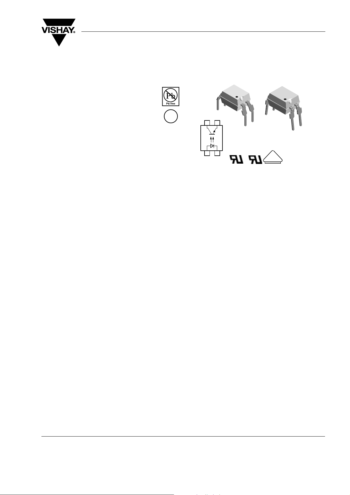
TCET1100/TCET1100G
Vishay Semiconductors
Optocoupler, Phototransistor Output, High Temperature
Features
• Extra low coupling capacity - typical 0.2 pF
• High Common Mode Rejection
• Low temperature coefficient of CTR
e3
• CTR offered in 9 groups
• Reinforced Isolation provides circuit protection
against electrical shock (Safety Class II)
• Lead-(Pb)-free component
• Component in accordance to RoHS 2002/95/EC
and WEEE 2002/96/EC
17197_1
C
E
4
3
12
AC
V
C
DE
Agency Approvals
• UL1577, File No. E76222 System Code U, Double
Protection
• CSA 22.2 bulletin 5A, Double Protection
• BSI: EN 60065:2002, EN 60950:2000
Certificate No. 7081 and 7402
• DIN EN 60747-5-2 (VDE0884)
DIN EN 60747-5-5 pending
• FIMKO
Applications
Switch-mode power supplies
Line receiver
Computer peripheral interface
Microprocessor system interface
Circuits for safe protective separation against electri-
cal shock according to safety class II (reinforced isolation):
• For appl. class I - IV at mains voltage ≤ 300 V
• For appl. class I - III at mains voltage ≤ 600 V accord-
ing to DIN EN 60747-5-2(VDE0884)/ DIN EN 607475-5 pending, table 2.
Description
The TCET110. consists of a phototransistor optically
coupled to a gallium arsenide infrared-emitting diode
in a 4-lead plastic dual inline package.
The elements are mounted on one leadframe using a
coplanar technique, providing a fixed distance
between input and output for highest safety requirements.
Isolation materials according to UL94-VO
Pollution degree 2 (DIN/VDE 0110 / resp. IEC 60664)
Climatic classification 55/100/21 (IEC 60068 part 1)
Rated impulse voltage (transient overvoltage)
V
= 8 kV peak
IOTM
Isolation test voltage (partial discharge test voltage)
V
= 1.6 kV
pd
Rated isolation voltage (RMS includes DC)
V
IOWM
= 600 V
(848 V peak)
RMS
Rated recurring peak voltage (repetitive)
V
= 600 V
IORM
RMS
Thickness through insulation ≥ 0.75 mm
Internal creepage distance > 4 mm
Creepage current resistance according to VDE 0303/
IEC 112 Comparative Tracking Index:
CTI ≥ 175
VDE Standards
These couplers perform safety functions according to
the following equipment standards:
DIN EN 60747-5-2(VDE0884)/ DIN EN 60747-5-5
pending
Optocoupler for electrical safety requirements
IEC 60950/EN 60950
Office machines (applied for reinforced isolation for
mains voltage ≤ 400 VRMS)
VDE 0804
Telecommunication apparatus and data processing
IEC 60065
Safety for mains-operated electronic and related
household apparatus
Document Number 83503
Rev. 2.2, 05-Sep-06
www.vishay.com
1
Page 2
TCET1100/TCET1100G
Vishay Semiconductors
Order Information
Par t Remarks
TCET1100 CTR 50 - 600 %, DIP-4
TCET1101 CTR 40 - 80 %, DIP-4
TCET1102 CTR 63 - 125 %, DIP-4
TCET1103 CTR 100 - 200 %, DIP-4
TCET1104 CTR 160 - 320 %, DIP-4
TCET1105 CTR 50 - 150 %, DIP-4
TCET1106 CTR 100 - 300 %, DIP-4
TCET1107 CTR 80 - 160 %, DIP-4
TCET1108 CTR 130 - 260 %, DIP-4
TCET1109 CTR 200 - 400 %, DIP-4
TCET1100G CTR 50 - 600 %, DIP-4
TCET1101G CTR 40 - 80 %, DIP-4
TCET1102G CTR 63 - 125 %, DIP-4
TCET1103G CTR 100 - 200 %, DIP-4
TCET1104G CTR 160 - 320 %, DIP-4
TCET1105G CTR 50 - 150 %, DIP-4
TCET1106G CTR 100 - 300 %, DIP-4
TCET1107G CTR 80 - 160 %, DIP-4
TCET1108G CTR 130 - 260 %, DIP-4
TCET1109G CTR 200 - 400 %, DIP-4
G = Leadform 10.16 mm; G is not marked on the body
Absolute Maximum Ratings
T
= 25 °C, unless otherwise specified
amb
Stresses in excess of the absolute Maximum Ratings can cause permanent damage to the device. Functional operation of the device is
not implied at these or any other conditions in excess of those given in the operational sections of this document. Exposure to absolute
Maximum Rating for extended periods of the time can adversely affect reliability.
Input
Parameter Test condition Symbol Val ue Unit
Reverse voltage
Forward current
Forward surge current
V
R
I
F
t
≤ 10 μsI
p
FSM
6V
60 mA
1.5 A
Output
Parameter Test condition Symbol Val ue Unit
Collector emitter voltage
Emitter collector voltage
Collector current
Collector peak current
/T = 0.5, tp ≤ 10 ms I
t
p
V
V
CEO
ECO
I
C
CM
70 V
7V
50 mA
100 mA
www.vishay.com
2
Document Number 83503
Rev. 2.2, 05-Sep-06
Page 3
TCET1100/TCET1100G
T
A
θ
CA
T
C
T
JD
T
JE
T
B
θ
EC
θ
EB
θ
DC
θ
DB
θ
BA
θ
DE
T
A
Vishay Semiconductors
Coupler
Parameter Test condition Symbol Value Unit
Isolation test voltage (RMS) t = 1 min
Operating ambient temperature
range
Storage temperature range
Soldering temperature 2 mm from case t ≤ 10 s
V
T
T
T
ISO
amb
stg
sld
5000
- 40 to + 100 °C
- 55 to + 125 °C
260 °C
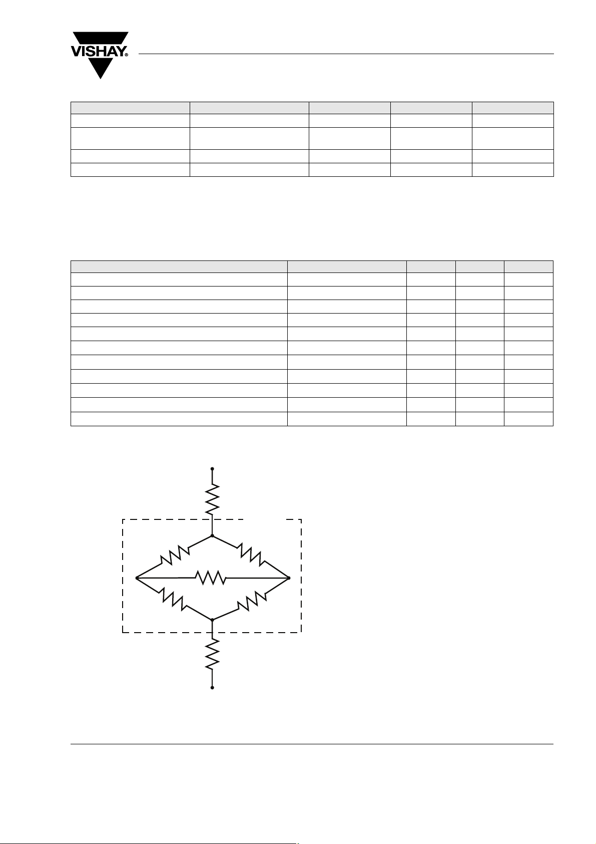
Thermal Characteristics
The thermal model is represented in the thermal network below. Each resistance value given in this model can be used to calculate the temperatures at each node for a given operating condition. The thermal resistance from board to ambient will be dependent on the type of PCB,
layout and thickness of copper traces. For a detailed explanation of the thermal model, please reference Vishay's Thermal Characteristics
of Optocouplers Application note.
Parameter Test condition Symbol Val ue Unit
LED Power dissipation at 25 °C P
Output Power dissipation at 25 °C P
Maximum LED junction temperature T
Maximum output die junction temperature T
Thermal resistance, Junction Emitter to Board
Thermal resistance, Junction Emitter to Case
Thermal resistance, Junction Detector to Board
Thermal resistance, Junction Detector to Case
Thermal resistance, Junction Emitter to Junction Detector
Thermal resistance, Board to Ambient*
Thermal resistance, Case to Ambient*
jmax
jmax
θ
θ
θ
θ
θ
θ
θ
diss
diss
EB
EC
DB
DC
ED
BA
CA
4041 °C/W
V
RMS
100 mW
150 mW
125 °C
125 °C
173 °C/W
149 °C/W
111 °C/W
127 °C/W
173 °C/W
197 °C/W
* For 2 layer FR4 board (4" x 3" x 0.062)
Package
19996
Document Number 83503
Rev. 2.2, 05-Sep-06
www.vishay.com
3
Page 4
TCET1100/TCET1100G
Vishay Semiconductors
Electrical Characteristics
T
= 25 °C, unless otherwise specified
amb
Minimum and maximum values are testing requirements. Typical values are characteristics of the device and are the result of engineering
evaluation. Typical values are for information only and are not part of the testing requirements.
Input
Parameter Test condition Symbol Min Ty p. Max Unit
= 50 mA V
Forward voltage
Junction capacitance
Output
Parameter Test condition Symbol Min Ty p. Max Unit
Collector emitter voltage
Emitter collector voltage
Collector-emitter cut-off current
Coupler
Parameter Test condition Symbol Min Ty p. Max Unit
Collector emitter saturation
voltage
Cut-off frequency V
Coupling capacitance f = 1 MHz
I
F
= 0 V, f = 1 MHz C
V
R
= 1 mA V
I
C
= 100 μAV
I
E
= 20 V, If = 0, E = 0 I
V
CE
= 10 mA, IC = 1 mA V
I
F
= 5 V, IF = 10 mA,
CE
= 100 Ω
R
L
F
j
CEO
ECO
CEO
CEsat
f
c
C
k
70 V
7V
1.25 1.6 V
50 pF
10 100 nA
0.3 V
110 kHz
0.3 pF
Current Transfer Ratio
Parameter Test condition Par t Symbol Min Ty p . Max Unit
I
C/IF
VCE = 5 V, IF = 1 mA
V
= 5 V, IF = 5 mA
CE
V
= 5 V, IF = 10 mA
CE
TCET1101
TCET1101G
TCET1102
TCET1102G
TCET1103
TCET1103G
TCET1104
TCET1104G
TCET1100
TCET1100G
TCET1105
TCET1105G
TCET1106
TCET1106G
TCET1107
TCET1107G
TCET1108
TCET1108G
TCET1109
TCET1109G
TCET1101
TCET1101G
TCET1102
TCET1102G
TCET1103
TCET1103G
TCET1104
TCET1104G
CTR 13 30 %
CTR 22 45 %
CTR 34 70 %
CTR 56 90 %
CTR 50 600 %
CTR 50 150 %
CTR 100 300 %
CTR 80 160 %
CTR 130 260 %
CTR 200 400 %
CTR 40 80 %
CTR 63 125 %
CTR 100 200 %
CTR 160 320 %
www.vishay.com
4
Document Number 83503
Rev. 2.2, 05-Sep-06
Page 5

TCET1100/TCET1100G
Maximum Safety Ratings
(according to DIN EN 60747-5-2(VDE0884)/ DIN EN 60747-5-5 pending) see figure 1.
This optocoupler is suitable for safe electrical isolation only within the safety ratings.
Compliance with the safety ratings shall be ensured by means of suitable protective circuits.
Input
Parameter Test condition Symbol Min Ty p . Max Unit
V
I
P
diss
IOTM
T
F
si
Forward current
Output
Parameter Test condition Symbol Min Ty p . Max Unit
Power dissipation
Coupler
Parameter Test condition Symbol Min Ty p . Max Unit
Rated impulse voltage
Safety temperature
Vishay Semiconductors
130 mA
265 mW
8kV
150 °C
Insulation Rated Parameters
Parameter Test condition Symbol Min Ty p . Max Unit
Partial discharge test voltage Routine test
Partial discharge test voltage Lot test (sample test)
Insulation resistance
300
250
200
150
100
50
tot
P - Total Power Dissipation (mW)
0
0 25 50 75 125
T
94 9182
- Safety Temperature (°C)
si
Figure 1. Derating diagram
IR-Diode
Isi (mA)
Phototransistor
Psi (mW)
100 %, t
test
= 60 s, t
t
Tr
(see figure 2)
= 500 V R
V
IO
= 500 V, T
V
IO
= 500 V, T
V
IO
(construction test only)
100
= 1 s V
= 10 s,
test
= 100 °C R
amb
= 150 °C
amb
150
Figure 2. Test pulse diagram for sample test according to DIN EN
1.6 kV
8kV
1.3 kV
12
10
11
10
9
10
t1, t2 = 1 to 10 s
t
, t4 = 1 s
3
t
= 10 s
test
= 12 s
t
stres
V
Pd
0
t
1
tTr = 60 s
V
pd
IOTM
V
pd
IO
IO
R
IO
V
V
IOWM
V
13930
IOTM
IORM
60747-5-2(VDE0884)/ DIN EN 60747-; IEC60747
t
2
t
t3t
test
t
stres
Ω
Ω
Ω
4
t
Document Number 83503
Rev. 2.2, 05-Sep-06
www.vishay.com
5
Page 6

TCET1100/TCET1100G
Vishay Semiconductors
Switching Characteristics
Parameter Test condition Symbol Min Ty p. Max Unit
Delay time V
Rise time V
Turn-on time V
Storage time V
Fall time V
Turn-off time V
Turn-on time V
Turn-off time V
I
I
F
0
F
RG = 50
t
p
= 0.01
T
tp = 50 µs
50 100
95 10804
Figure 3. Test circuit, non-saturated operation
= 5 V, IC = 2 mA, RL = 100 Ω
S
(see figure 3)
= 5 V, IC = 2 mA, RL = 100 Ω
S
(see figure 3)
= 5 V, IC = 2 mA, RL = 100 Ω
S
(see figure 3)
= 5 V, IC = 2 mA, RL = 100 Ω
S
(see figure 3)
= 5 V, IC = 2 mA, RL = 100 Ω
S
(see figure 3)
= 5 V, IC = 2 mA, RL = 100 Ω
S
(see figure 3)
= 5 V, IF = 10 mA, RL = 1 kΩ
S
(see figure 4)
= 5 V, IF = 10 mA, RL = 1 kΩ
S
(see figure 4)
+ 5 V
IC = 2 mA;
Channel I
Channel II
adjusted through
input amplitude
Oscilloscope
= 1 M
R
L
= 20 pF
C
L
t
d
t
r
t
on
t
s
t
f
t
off
t
on
t
off
I
F
0
I
C
100 %
90 %
10 %
t
p
t
d
t
r
t
on
(=t + t )
d
0
r
t
t
d
t
on
pulse duration
delay time
rise time
turn-on time
3.0 µs
3.0 µs
6.0 µs
0.3 µs
4.7 µs
5.0 µs
9.0 µs
10.0 µs
t
p
r
t
t
f
s
t
off
t
s
t
f
t
(= ts+tf)turn-off time
off
96 11698
t
t
storage time
fall time
Figure 5. Switching Times
I
F
0
R G =5 0
Ω
t
p
= 0.01
T
t p =5 0 µs
95 10843
Figure 4. Test circuit, saturated operation
www.vishay.com
6
50
I
F
=1 0m A
Ω
1k
Ω
+5V
I
C
Channel I
Channel II
Oscilloscope
Ω
R
M 1
≥
L
C
20 pF
≤
L
Document Number 83503
Rev. 2.2, 05-Sep-06
Page 7

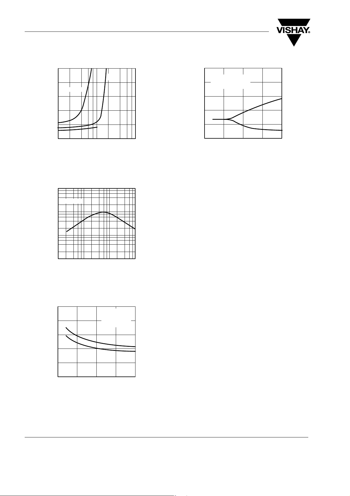
Typical Characteristics
1000
C
T
= 25 °C, unless otherwise specified
amb
TCET1100/TCET1100G
Vishay Semiconductors
300
Coupled device
250
200
Phototransistor
150
IR-diode
100
50
tot
P - Total Power Dissipation (mW)
0
04080 120
T
96 11700
- Ambient Temperature (°C)
amb
Figure 6. Total Power Dissipation vs. Ambient Temperature
100
urrent (mA)
10
10000
VCE= 20 V
= 0
I
1000
F
100
with open Base (nA)
10
CEO
I - Collector Dark Current,
1
0255075
95 11026
- Ambient Temperature (°C)
T
amb
100
Figure 9. Collector Dark Current vs. Ambient Temperature
100
VCE = 5 V
10
1
1
F
I - Forward
0.1
0
0.2
0.4
0.8 0.6
1.0
- Forward Voltage (V) 96 11862
V
F
1.2
1.4
1.6
1.8
Figure 7. Forward Current vs. Forward Voltage
2.0
1.5
1.0
0.5
rel
0
CTR - Relative Current Transfer Ratio
- 25 0 25 50
95 11025
T
- Ambient Temperature (°C)
amb
VCE = 5 V
= 5 mA
I
F
Figure 8. Relative Current Transfer Ratio vs.
Ambient Temperature
2.0
0.1
C
I - Collector Current (mA)
0.01
0.1 1 10
95 11027
IF- Forward Current (mA)
100
Figure 10. Collector Current vs. Forward Current
100
IF= 50 mA
10
1
C
I - Collector Current (mA)
0.1
75
0.1 1 10
- Collector Emitter Voltage (V)
95 10985
V
CE
20 mA
10 mA
5 mA
2 mA
1 mA
100
Figure 11. Collector Current vs. Collector Emitter Voltage
Document Number 83503
Rev. 2.2, 05-Sep-06
www.vishay.com
7
Page 8
TCET1100/TCET1100G
Vishay Semiconductors
1.0
20 %
0.8
CTR = 50 %
0.6
0.4
0.2
0
110
CEsat
V - Collector Emitter Saturation Voltage (V)
95 11028
IC- Collector Current (mA)
10 %
100
Figure 12. Collector Emitter Saturation Voltage vs.
Collector Current
1000
VCE = 5 V
100
10
50
Saturated Operation
= 5 V
V
S
= 1 kΩ
R
L
t
off
t
0
01015
5
- Forward Current (mA)
I
F
on
20
offon
t/t - Turn on/Turn off Time (µs)
95 11031
40
30
20
10
Figure 15. Turn on/off Time vs. Forward Current
CTR - Current Transfer Ratio (%)
1
0.1 1 10
95 11029
IF- Forward Current (mA)
100
Figure 13. Current Transfer Ratio vs. Forward Current
10
8
t
on
6
t
off
4
2
offon
t/t- Turn on /Turn off Time (µs)
0
04
95 11030
2
- Collector Current (mA)
I
C
Non Saturated
Operation
V
= 5 V
S
R
= 100 Ω
L
6
8
Figure 14. Turn on/off Time vs. Collector Current
www.vishay.com
8
Document Number 83503
Rev. 2.2, 05-Sep-06
Page 9
Package Dimensions in mm
TCET1100/TCET1100G
Vishay Semiconductors
Package Dimensions in mm
14789
Document Number 83503
Rev. 2.2, 05-Sep-06
14792
www.vishay.com
9
Page 10

TCET1100/TCET1100G
Vishay Semiconductors
Ozone Depleting Substances Policy Statement
It is the policy of Vishay Semiconductor GmbH to
1. Meet all present and future national and international statutory requirements.
2. Regularly and continuously improve the performance of our products, processes, distribution and operating
systems with respect to their impact on the health and safety of our employees and the public, as well as
their impact on the environment.
It is particular concern to control or eliminate releases of those substances into the atmosphere which are
known as ozone depleting substances (ODSs).
The Montreal Protocol (1987) and its London Amendments (1990) intend to severely restrict the use of ODSs
and forbid their use within the next ten years. Various national and international initiatives are pressing for an
earlier ban on these substances.
Vishay Semiconductor GmbH has been able to use its policy of continuous improvements to eliminate the use
of ODSs listed in the following documents.
1. Annex A, B and list of transitional substances of the Montreal Protocol and the London Amendments
respectively
2. Class I and II ozone depleting substances in the Clean Air Act Amendments of 1990 by the Environmental
Protection Agency (EPA) in the USA
3. Council Decision 88/540/EEC and 91/690/EEC Annex A, B and C (transitional substances) respectively.
Vishay Semiconductor GmbH can certify that our semiconductors are not manufactured with ozone depleting
substances and do not contain such substances.
We reserve the right to make changes to improve technical design
and may do so without further notice.
Parameters can vary in different applications. All operating parameters must be validated for each
customer application by the customer. Should the buyer use Vishay Semiconductors products for any
unintended or unauthorized application, the buyer shall indemnify Vishay Semiconductors against all
claims, costs, damages, and expenses, arising out of, directly or indirectly, any claim of personal
damage, injury or death associated with such unintended or unauthorized use.
Vishay Semiconductor GmbH, P.O.B. 3535, D-74025 Heilbronn, Germany
www.vishay.com
10
Document Number 83503
Rev. 2.2, 05-Sep-06
Page 11

Legal Disclaimer Notice
Vishay
Document Number: 91000 www.vishay.com
Revision: 08-Apr-05 1
Notice
Specifications of the products displayed herein are subject to change without notice. Vishay Intertechnology, Inc.,
or anyone on its behalf, assumes no responsibility or liability for any errors or inaccuracies.
Information contained herein is intended to provide a product description only. No license, express or implied, by
estoppel or otherwise, to any intellectual property rights is granted by this document. Except as provided in Vishay's
terms and conditions of sale for such products, Vishay assumes no liability whatsoever, and disclaims any express
or implied warranty, relating to sale and/or use of Vishay products including liability or warranties relating to fitness
for a particular purpose, merchantability, or infringement of any patent, copyright, or other intellectual property right.
The products shown herein are not designed for use in medical, life-saving, or life-sustaining applications.
Customers using or selling these products for use in such applications do so at their own risk and agree to fully
indemnify Vishay for any damages resulting from such improper use or sale.
 Loading...