

Page 1
www.vishay.com
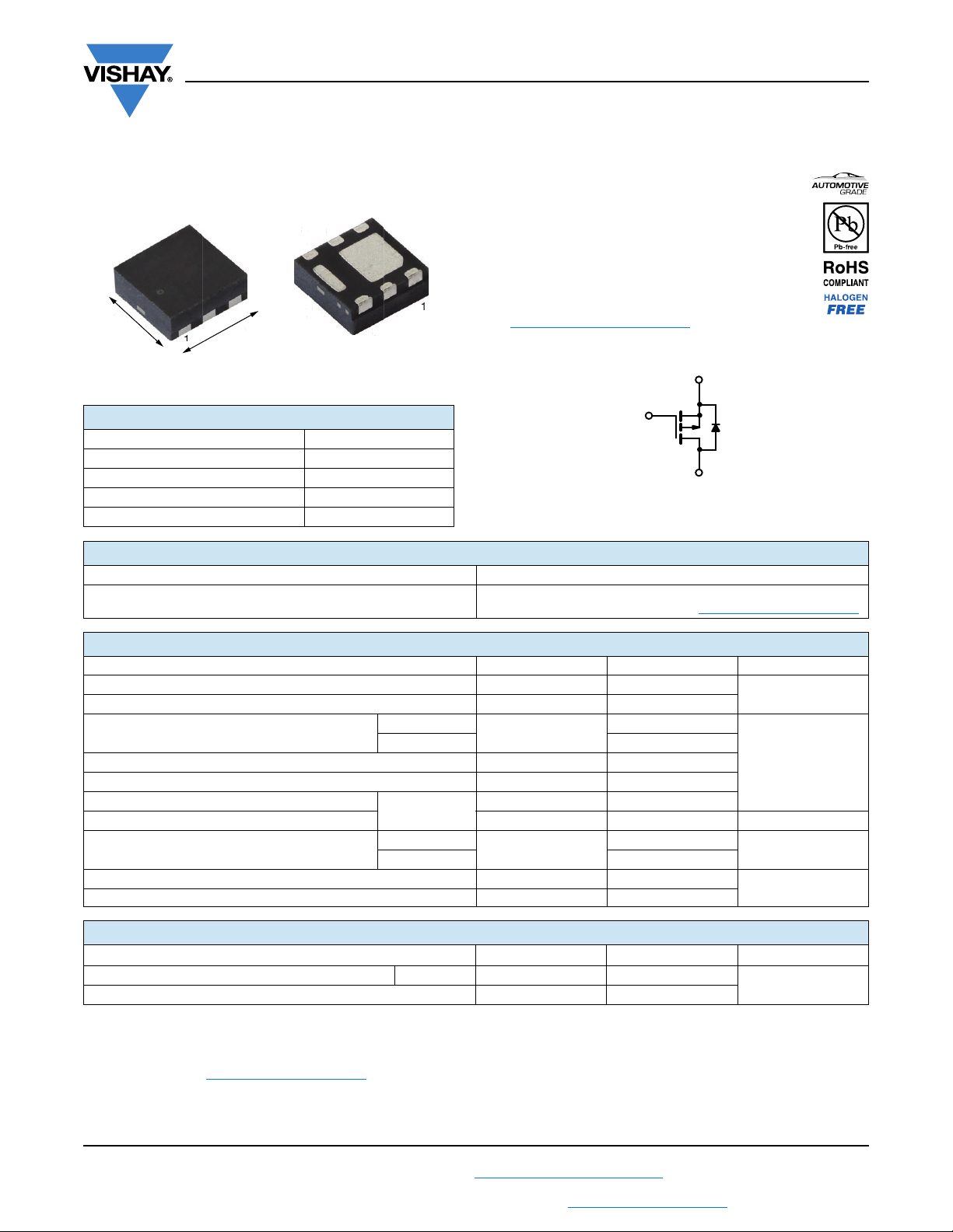
PowerPAK® SC-70W-6L Single
Top View
2.05 mm
2.05 mm
1
m
2.05 mm
Bottom View
3
G
2
D
1
D
S
4
D
5
D
6
S
7
21DS4
D
5
6
S
7
S
G
D
P-Channel MOSFET
Automotive P-Channel 20 V (D-S) 175 °C MOSFET
Marking Code: QKXXXX
PRODUCT SUMMARY
VDS (V) -20
R
(Ω) at VGS = -4.5 V 0.125
DS(on)
R
(Ω) at VGS = -2.5 V 0.219
DS(on)
I
(A) -3.75
D
Configuration Single
FEATURES
• TrenchFET® power MOSFET
• AEC-Q101 qualified
• Wettable flank terminals
• 100 % R
• Material categorization:
for definitions of compliance please see
www.vishay.com/doc?99912
and UIS tested
g
SQA401CEJW
Vishay Siliconix
ORDERING INFORMATION
Package PowerPAK SC-70W-6L
Lead (Pb)-free and halogen-free
SQA401CEJW
(for detailed order number please see www.vishay.com/doc?79776
ABSOLUTE MAXIMUM RATINGS (TC = 25 °C, unless otherwise noted)
PARAMETER SYMBOL LIMIT UNIT
Drain-source voltage V
Gate-source voltage V
a
TC = 25 °C
T
= 125 °C -3.75
C
L = 0.1 mH
T
= 25 °C
C
= 125 °C 4.5
T
C
Continuous drain current
a
Continuous source current (diode conduction)
Pulsed drain current
b
Single pulse avalanche current
Single pulse avalanche energy E
Maximum power dissipation
Operating junction and storage temperature range T
Soldering recommendations (peak temperature)
d, e
DS
± 12
GS
I
D
I
S
IDM -12
I
AS
AS
P
D
, T
J
stg
-20
-3.75
-3.75
-8
3.2 mJ
13.6
-55 to +175
260
THERMAL RESISTANCE RATINGS
PARAMETER SYMBOL LIMIT UNIT
Junction-to-ambient PCB mount
c
Junction-to-case (drain) R
Notes
a. Package limited
b. Pulse test; pulse width ≤ 300 μs, duty cycle ≤ 2 %
c. When mounted on 1" square PCB (FR4 material)
d. See solder profile (www.vishay.com/doc?73257
The end of the lead terminal is plated with tin
e. Rework conditions: manual soldering with a soldering iron is not recommended for leadless components
f. Not intended for continuous use with positive gate voltage > 3.0 V
). The PowerPAK SC-70W-6L is a leadless package and features wettable flank terminals.
R
thJA
thJF
90
11
)
V
A
W
°C
°C/W
S21-0091-Rev. A, 08-Feb-2021
THIS DOCUMENT IS SUBJECT TO CHANGE WITHOUT NOTICE. THE PRODUCTS DESCRIBED HEREIN AND THIS DOCUMENT
ARE SUBJECT TO SPECIFIC DISCLAIMERS, SET FORTH AT www.vishay.com/doc?91000
For technical questions, contact: automostechsupport@vishay.com
1
Document Number: 66844
Page 2
SQA401CEJW
www.vishay.com
SPECIFICATIONS (TC = 25 °C, unless otherwise noted)
PARAMETER SYMBOL TEST CONDITIONS MIN. TYP. MAX. UNIT
Static
Drain-source breakdown voltage V
Gate-source threshold voltage V
Gate-source leakage I
Zero gate voltage drain current I
On-state drain current
Drain-source on-state resistance
Forward transconductance
Dynamic
b
a
a
b
Input capacitance C
Reverse transfer capacitance C
Total gate charge
Gate-drain charge
c
c
c
Gate resistance R
Turn-on delay time
Rise time
c
Turn-off delay time
Fall time
c
c
c
I
R
t
t
DS
GS(th)
GSS
DSS
D(on)
DS(on)
g
fs
iss
oss
rss
Q
g
Q
gs
Q
gd
g
d(on)
t
r
d(off)
t
f
Source-Drain Diode Ratings and Characteristics
Pulsed current
Forward voltage V
Body diode reverse recovery time t
Body diode reverse recovery charge Q
Reverse recovery fall time t
Reverse recovery rise time t
Body diode peak reverse recovery current I
a
I
SM
SD
rr
rr
-9-
a
b
RM(REC)
Notes
a. Pulse test; pulse width ≤ 300 μs, duty cycle ≤ 2 %
b. Guaranteed by design, not subject to production testing
c. Independent of operating temperature
VGS = -4.5 V VDS ≥ 5 V -8 - - A
VGS = -4.5 V ID = -2.4 A - 0.085 0.125
V
V
V
VGS = -4.5 V VDS = -10 V, ID = -2.4 A
VGS = 0, ID = -250 μA -20 - -
VDS = VGS, ID = -250 μA -0.6 -1.0 -1.3
VDS = 0 V, VGS = ± 12 V - - ± 100 nA
VGS = 0 V VDS = -20 V - - -1
= 0 V VDS = -20 V, TJ = 125 °C - - -50
GS
V
= 0 V VDS = -20 V, TJ = 175 °C - - -150
GS
= -4.5 V ID = -2.4 A, TJ = 125 °C - - 0.175
GS
= -4.5 V ID = -2.4 A, TJ = 175 °C - - 0.200
GS
= -2.5 V ID = -1.8 A - 0.160 0.219
GS
VDS = -10 V, ID = -2.4 A - 6 - S
VGS = 0 V VDS = -10 V, f = 1 MHz
f = 1 MHz 2.8 5.6 8.4 Ω
VDD = -10 V, RL = 5.21 Ω
I
≅ -1.9 A, V
D
= -4.5 V, Rg = 1 Ω
GEN
IF = -2 A, V
= 0 - -0.8 -1.2 V
GS
IF = -1.5 A, di/dt = 100 A/μs
Vishay Siliconix
- 265 330
-7594
-5063
-3.55.5
-0.9-
-1.2-
-2030
-1827
-1928
-812
---12A
-2244ns
-1224nC
-13-
--1-A
V
μA V
Ω
pF Output capacitance C
nC Gate-source charge
ns
ns
Stresses beyond those listed under “Absolute Maximum Ratings” may cause permanent damage to the device. These are stress ratings only, and functional operation
of the device at these or any other conditions beyond those indicated in the operational sections of the specifications is not implied. Exposure to absolute maximum
rating conditions for extended periods may affect device reliability.
S21-0091-Rev. A, 08-Feb-2021
2
Document Number: 66844
For technical questions, contact: automostechsupport@vishay.com
THIS DOCUMENT IS SUBJECT TO CHANGE WITHOUT NOTICE. THE PRODUCTS DESCRIBED HEREIN AND THIS DOCUMENT
ARE SUBJECT TO SPECIFIC DISCLAIMERS, SET FORTH AT www.vishay.com/doc?91000
Page 3

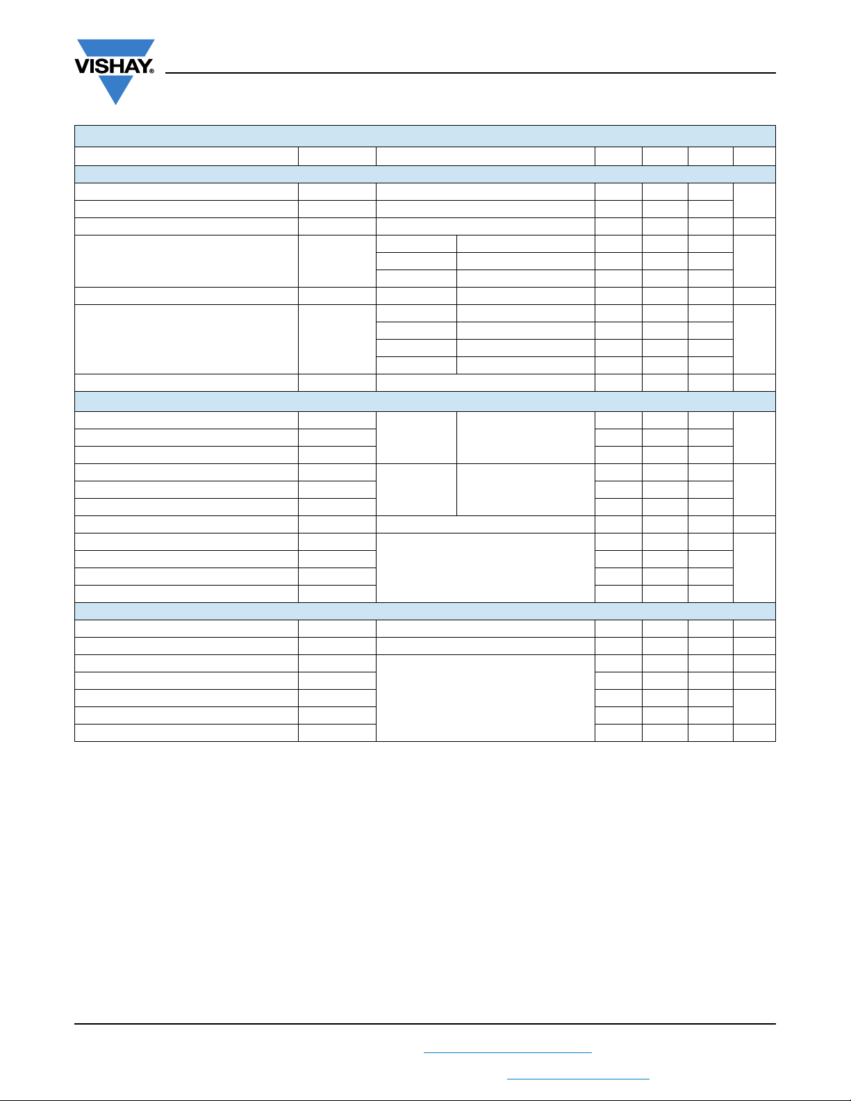
10
100
1000
10000
0
4
8
12
16
20
012345
Axis Title
1st line
2nd line
2nd line
I
D
- Drain Current (A)
VDS- Drain-to-Source Voltage (V)
VGS= 4.5 V
VGS= 2 V
VGS= 2.5 V
VGS= 3 V
VGS= 3.5 V
VGS= 4 V
VGS= 5 V
10
100
1000
10000
10
100
1000
0 4 8 12 16 20
Axis Title
1st line
2nd line
2nd line
C - Capacitance (pF)
VDS- Drain-to-Source Voltage (V)
C
rss
C
oss
10
100
1000
10000
0
2
4
6
8
10
012345
Axis Title
1st line
2nd line
2nd line
I
D
- Drain Current (A)
VGS- Gate-to-Source Voltage (V)
TC= 25 °C
TC= -55 °C
TC= 125 °C
10
100
1000
10000
0.0
0.1
0.2
0.3
0.4
0.5
0246810
Axis Title
1st line
2nd line
2nd line
R
DS(on)
- On-Resistance (Ω)
ID- Drain Current (A)
VGS= 4.5 V
VGS= 2.5 V
10
100
1000
10000
0
1
2
3
4
5
012345
Axis Title
1st line
2nd line
2nd line
V
GS
- Gate-to-Source Voltage (V)
Qg- Total Gate Charge (nC)
ID= 2.4 A
V
DS
= 10 V
www.vishay.com
TYPICAL CHARACTERISTICS (TA = 25 °C, unless otherwise noted)
SQA401CEJW
Vishay Siliconix
Output Characteristics
10
8
TC= 25 °C
6
2nd line
4
- Transconductance (S)
fs
2
g
0
012345
ID- Drain Current (A)
TC= -55 °C
TC= 125 °C
Transconductance
C
iss
Transfer Characteristics
On-Resistance vs. Drain Current
S21-0091-Rev. A, 08-Feb-2021
THIS DOCUMENT IS SUBJECT TO CHANGE WITHOUT NOTICE. THE PRODUCTS DESCRIBED HEREIN AND THIS DOCUMENT
Capacitance
ARE SUBJECT TO SPECIFIC DISCLAIMERS, SET FORTH AT www.vishay.com/doc?91000
Gate Charge
3
For technical questions, contact: automostechsupport@vishay.com
Document Number: 66844
Page 4

10
100
1000
10000
0.5
0.8
1.1
1.4
1.7
2.0
-50 -25 0 25 50 75 100 125 150 175
Axis Title
1st line
2nd line
2nd line
R
DS(on)
- On-Resistance (Normalized)
TJ- Junction Temperature (°C)
VGS= 4.5 V
VGS= 2.5 V
10
100
1000
10000
0
0.2
0.4
0.6
0.8
1.0
012345
Axis Title
1st line
2nd line
2nd line
R
DS(on)
- On-Resistance (Ω)
VGS- Gate-to-Source Voltage (V)
TJ= 150 °C
TJ= 25 °C
10
100
1000
10000
0.01
0.1
1
10
100
0 0.2 0.4 0.6 0.8 1.0 1.2
Axis Title
1st line
2nd line
2nd line
I
S
- Source Current (A)
VSD- Source-to-Drain Voltage (V)
TJ= 25 °C
TJ= 150 °C
10
100
1000
10000
-0.4
-0.2
0
0.2
0.4
0.6
-50 -25 0 25 50 75 100 125 150 175
Axis Title
1st line
2nd line
2nd line
V
GS(th)
- Variance (V)
TJ- Junction Temperature (°C)
ID= 250 μA
10
100
1000
10000
-28
-27
-26
-25
-24
-23
-50 -25 0 25 50 75 100 125 150 175
Axis Title
1st line
2nd line
2nd line
V
DS
- Drain-to-Source Voltage (V)
TJ- Junction Temperature (°C)
www.vishay.com
TYPICAL CHARACTERISTICS (TA = 25 °C, unless otherwise noted)
ID= 2.5 A
SQA401CEJW
Vishay Siliconix
ID= 5 mA
On-Resistance vs. Junction Temperature
On-Resistance vs. Gate-to-Source Voltage
Threshold Voltage
ID= 10 mA
Drain Source Breakdown vs. Junction Temperature
100
IDMlimited
10
Axis Title
100 us
10000
1000
1
2nd line
S21-0091-Rev. A, 08-Feb-2021
Source-Drain Diode Forward Voltage
4
THIS DOCUMENT IS SUBJECT TO CHANGE WITHOUT NOTICE. THE PRODUCTS DESCRIBED HEREIN AND THIS DOCUMENT
ARE SUBJECT TO SPECIFIC DISCLAIMERS, SET FORTH AT www.vishay.com/doc?91000
For technical questions, contact: automostechsupport@vishay.com
- Drain Current (A)
D
I
0.1
0.01
0.01 0.1 1 10 100
Note
> minimum VGS at which R
a. V
GS
Limited by R
TC= 25 °C,
single pulse
VDS- Drain-to-Source Voltage (V)
Safe Operating Area
IDlimited
a
DS(on)
BVDSS limited
DS(on)
1 ms
10 ms
100 ms, 1 s, 10 s, DC
100
10
is specified
Document Number: 66844
1st line
2nd line
Page 5

10
-3
10
-2
1 10 60010
-1
10
-4
100
2
1
0.1
0.01
0.2
0.1
0.05
0.02
Single pulse
Duty cycle = 0.5
Square Wave Pulse Duration (s)
tneisnarT evitceffE dezilamroN
ecnadepmI lam
r
e
hT
1. Duty cycle, D =
2. Per unit base = R
thJA
= 90 °C/W
3. T
JM
- TA = PDMZ
thJA
(t)
t
1
t
2
t
1
t
2
Notes:
4. Surface mounted
P
DM
www.vishay.com
THERMAL RATINGS (TA = 25 °C, unless otherwise noted)
Normalized Thermal Transient Impedance, Junction-to-Ambient
SQA401CEJW
Vishay Siliconix
2
1
tneisnarT evitceffE dezilam
Duty cycle = 0.5
ecnad
e
p
mI lamrehT
0.2
0.1
0.1
0.05
r
oN
0.02
Single pulse
0.01
-4
10
-3
10
-2
10
-1
11010
Square Wave Pulse Duration (s)
Normalized Thermal Transient Impedance, Junction-to-Case
5
Document Number: 66844
Vishay Siliconix maintains worldwide manufacturing capability. Products may be manufactured at one of several qualified locations. Reliability data for Silicon
Technology and Package Reliability represent a composite of all qualified locations. For related documents such as package / tape drawings, part marking, and
reliability data, see www.vishay.com/ppg?66844
.
S21-0091-Rev. A, 08-Feb-2021
For technical questions, contact: automostechsupport@vishay.com
THIS DOCUMENT IS SUBJECT TO CHANGE WITHOUT NOTICE. THE PRODUCTS DESCRIBED HEREIN AND THIS DOCUMENT
ARE SUBJECT TO SPECIFIC DISCLAIMERS, SET FORTH AT www.vishay.com/doc?91000
Page 6

Legal Disclaimer Notice
www.vishay.com
Vishay
Disclaimer
ALL PRODUCT, PRODUCT SPECIFICATIONS AND DATA ARE SUBJECT TO CHANGE WITHOUT NOTICE TO IMPROVE
RELIABILITY, FUNCTION OR DESIGN OR OTHERWISE.
Vishay Intertechnology, Inc., its affiliates, agents, and employees, and all persons acting on its or their behalf (collectively,
“Vishay”), disclaim any and all liability for any errors, inaccuracies or incompleteness contained in any datasheet or in any other
disclosure relating to any product.
Vishay makes no warranty, representation or guarantee regarding the suitability of the products for any particular purpose or
the continuing production of any product. To the maximum extent permitted by applicable law, Vishay disclaims (i) any and all
liability arising out of the application or use of any product, (ii) any and all liability, including without limitation special,
consequential or incidental damages, and (iii) any and all implied warranties, including warranties of fitness for particular
purpose, non-infringement and merchantability.
Statements regarding the suitability of products for certain types of applications are based on Vishay’s knowledge of
typical requirements that are often placed on Vishay products in generic applications. Such statements are not binding
statements about the suitability of products for a particular application. It is the customer’s responsibility to validate that a
particular product with the properties described in the product specification is suitable for use in a particular application.
Parameters provided in datasheets and / or specifications may vary in different applications and performance may vary over
time. All operating parameters, including typical parameters, must be validated for each customer application by the customer’s
technical experts. Product specifications do not expand or otherwise modify Vishay’s terms and conditions of purchase,
including but not limited to the warranty expressed therein.
Except as expressly indicated in writing, Vishay products are not designed for use in medical, life-saving, or life-sustaining
applications or for any other application in which the failure of the Vishay product could result in personal injury or death.
Customers using or selling Vishay products not expressly indicated for use in such applications do so at their own risk.
Please contact authorized Vishay personnel to obtain written terms and conditions regarding products designed for
such applications.
No license, express or implied, by estoppel or otherwise, to any intellectual property rights is granted by this document
or by any conduct of Vishay. Product names and markings noted herein may be trademarks of their respective owners.
© 2021 VISHAY INTERTECHNOLOGY, INC. ALL RIGHTS RESERVED
Revision: 01-Jan-2021
1
Document Number: 91000
 Loading...