

Page 1
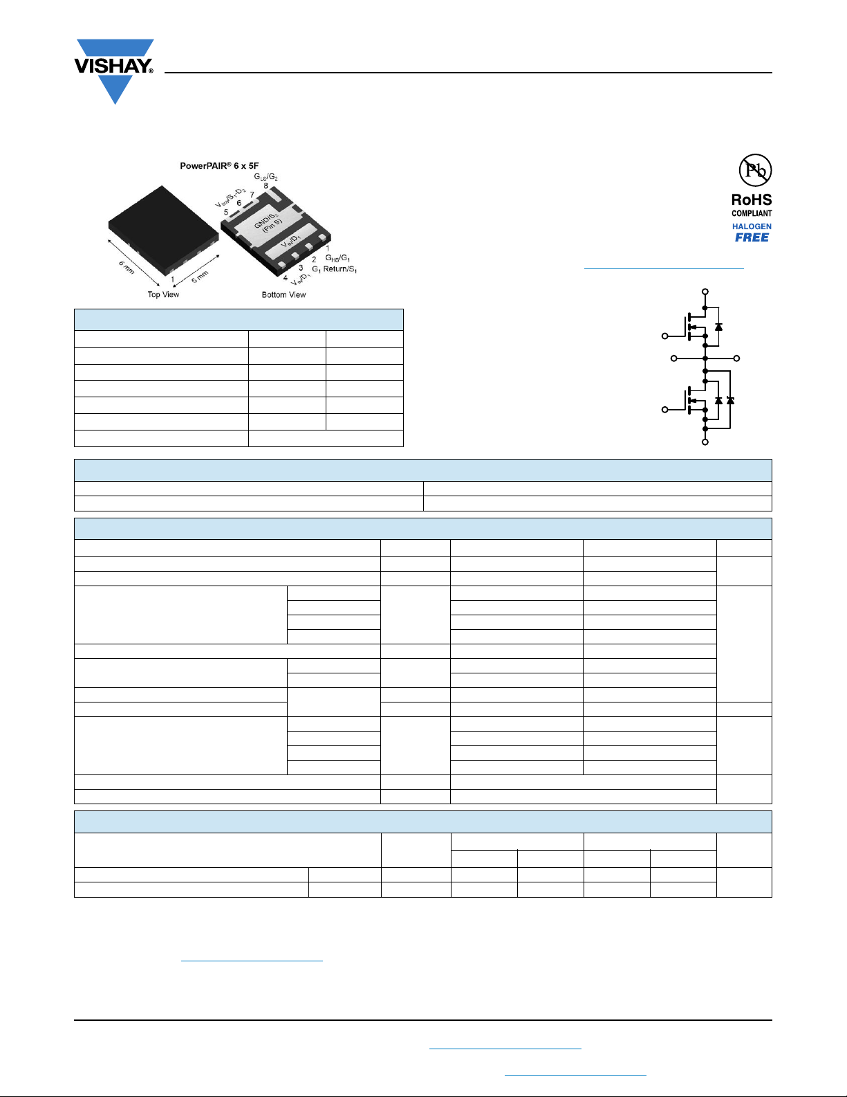
SiZF906BDT
www.vishay.com
Vishay Siliconix
Dual N-Channel 30 V (D-S) MOSFET with Schottky Diode
FEATURES
• TrenchFET® Gen IV power MOSFET
®
•SkyFET
Schottky
• 100 % Rg and UIS tested
• Material categorization: for definitions of
compliance please see www.vishay.com/doc?99912
low side MOSFET with integrated
VIN/D
1
VSW/S1-D
Schottky
Diode
2
2
1
GND/S
PRODUCT SUMMARY
CHANNEL-1 CHANNEL-2
V
(V) 30 30
DS
R
max. () at VGS = 10 V 0.00210 0.00068
DS(on)
R
max. () at VGS = 4.5 V 0.00370 0.00130
DS(on)
Q
typ. (nC) 11.7 38
g
a
I
(A)
D
Configuration Dual
105 257
APPLICATIONS
• CPU core power
• Computer / server peripherals
•POL
• Synchronous buck converter
• Telecom DC/DC
N-Channel 1
MOSFET
GHS/G
1
G1Return/S
GLS/G
2
N-Channel 2
MOSFET
ORDERING INFORMATION
Package PowerPAIR 6 x 5F
Lead (Pb)-free and halogen-free SiZF906BDT-T1-GE3
ABSOLUTE MAXIMUM RATINGS (TA = 25 °C, unless otherwise noted)
PARAMETER SYMBOL CHANNEL-1 CHANNEL-2 UNIT
Drain-source voltage V
Gate-source voltage V
= 25 °C
T
C
= 70 °C 84 206
T
Continuous drain current (T
= 150 °C)
J
C
= 25 °C 36
T
A
TA = 70 °C 29
Pulsed drain current (t = 100 μs) I
= 25 °C
T
Continuous source-drain diode current
Single pulse avalanche current
Single pulse avalanche energy E
Maximum power dissipation
C
TA = 25 °C 4.1
L = 0.1 mH
= 25 °C
T
C
= 70 °C 24 53
T
C
= 25 °C 4.5
T
A
I
P
TA = 70 °C 2.9
Operating junction and storage temperature range TJ, T
d, e
Soldering recommendations (peak temperature)
260
DS
GS
I
D
DM
I
AS
AS
S
D
stg
30 30
+20, -16 +20, -16
105 257
b, c
b, c
63
50
b, c
b, c
120 350
8.5
a
b, c
34 141
b, c
23 40
26.5 80 mJ
38 83
b, c
b, c
5
3.2
b, c
b, c
-55 to +150
V
A
W
°C
THERMAL RESISTANCE RATINGS
PARAMETER SYMBOL
Maximum junction-to-ambient
b, f
Maximum junction-to-case (source) Steady state R
t 10 s R
thJA
thJC
Notes
a. T
= 25 °C
C
b. Surface mounted on 1" x 1" FR4 board
c. t = 20 s
d. See solder profile (www.vishay.com/doc?73257
plated) as a result of the singulation process in manufacturing. A solder fillet at the exposed copper tip cannot be guaranteed and is not
required to ensure adequate bottom side solder interconnection
). The PowerPAIR is a leadless package. The end of the lead terminal is exposed copper (not
e. Rework conditions: manual soldering with a soldering iron is not recommended for leadless components
f. Maximum under steady state conditions is 60 °C/W for channel-1 and 60 °C/W for channel-2
S20-0516-Rev. A, 29-Jun-2020
1
For technical questions, contact: pmostechsupport@vishay.com
THIS DOCUMENT IS SUBJECT TO CHANGE WITHOUT NOTICE. THE PRODUCTS DESCRIBED HEREIN AND THIS DOCUMENT
ARE SUBJECT TO SPECIFIC DISCLAIMERS, SET FORTH AT www.vishay.com/doc?91000
CHANNEL-1 CHANNEL-2
TYP. MAX. TYP. MAX.
22 28 20 25
2.6 3.3 1.2 1.5
Document Number: 77619
UNIT
°C/W
Page 2
SiZF906BDT
www.vishay.com
SPECIFICATIONS (TJ = 25 °C, unless otherwise noted)
PARAMETER SYMBOL TEST CONDITIONS MIN. TYP. MAX. UNIT
Static
V
= 0 V, ID = 250 μA Ch-1 30 - -
Drain-source breakdown voltage V
Drain-source breakdown voltage
(transient)
c
V
Gate-source threshold voltage V
Gate-source leakage I
Zero Gate voltage drain current I
On-state drain current
Drain-source on-state resistance
Forward transconductance
Dynamic
a
b
b
b
I
R
Input capacitance C
Output capacitance C
Reverse transfer capacitance C
C
ratio
rss/Ciss
Total gate charge Q
Gate-source charge Q
Gate-drain charge Q
Output charge Q
Gate resistance R
DS
DSt
GS(th)
GSS
DSS
V
D(on)
DS(on)
g
fs
iss
oss
rss
g
gs
gd
oss
g
GS
= 0 V, ID = 5 mA Ch-2 30 - -
V
GS
V
= 0 V, t
GS
(transient)
VDS = VGS, ID = 250 μA
V
= 0 V, V
V
DS
DS
= 30 V, V
GS
V
= 30 V, V
DS
GS
5 V, V
DS
V
= 10 V, ID = 15 A Ch-1 - 0.00150 0.00210
GS
V
= 10 V, ID = 20 A Ch-2 - 0.00045 0.00068
GS
V
= 4.5 V, ID = 10 A Ch-1 - 0.00250 0.00370
GS
V
= 4.5 V, ID = 15 A Ch-2 - 0.00085 0.00130
GS
V
= 10 V, ID = 40 A Ch-1 - 93 -
DS
V
= 10 V, ID = 30 A Ch-2 170 -
DS
Channel-1
V
= 15 V, V
DS
GS
Channel-2
= 15 V, V
V
DS
= 15 V, V
V
DS
GS
GS
Channel-1
V
= 15 V, V
DS
GS
Channel-2
= 15 V, V
V
DS
GS
VDS = 15 V, VGS = 0 V
f = 1 MHz
1 μs
= +20 V, -16 V
= 0 V
GS
= 0 V, TJ = 55 °C
= 10 V
GS
= 0 V, f = 1 MHz
= 0 V, f = 1 MHz
= 10 V, ID = 20 A
= 4.5 V, ID = 20 A
= 4.5 V, ID = 20 A
Ch-1 36 - -
Ch-2 36 - -
Ch-1 1.1 - 2.2
Ch-2 1.1 - 2.2
Ch-1 - - ± 100
Ch-2 - - ± 100
Ch-1 - - 1
Ch-2 - 100 1000
Ch-1 - - 5
Ch-2 - 500 5000
Ch-1 20 - -
Ch-2 20 - -
Ch-1 - 1630 -
Ch-2 - 5550 -
Ch-1 - 690 -
Ch-2 - 2320 -
Ch-1 - 50 -
Ch-2 - 205 -
Ch-1 - 0.030 0.060
Ch-2 0.037 0.080
Ch-1 - 25 49
Ch-2 - 81 165
Ch-1 11.7 22
Ch-2 - 38 80
Ch-1 - 5.8 -
Ch-2 - 17.8 -
Ch-1 - 2.9 -
Ch-2 - 8.4 -
Ch-1 - 18 -
Ch-2 - 65 -
Ch-1 0.2 1.2 2
Ch-2 0.12 0.6 1.2
Vishay Siliconix
V
nA
μA
A
S
pF
nC
S20-0516-Rev. A, 29-Jun-2020
2
Document Number: 77619
For technical questions, contact: pmostechsupport@vishay.com
THIS DOCUMENT IS SUBJECT TO CHANGE WITHOUT NOTICE. THE PRODUCTS DESCRIBED HEREIN AND THIS DOCUMENT
ARE SUBJECT TO SPECIFIC DISCLAIMERS, SET FORTH AT www.vishay.com/doc?91000
Page 3
SiZF906BDT
www.vishay.com
SPECIFICATIONS (TJ = 25 °C, unless otherwise noted)
PARAMETER SYMBOL TEST CONDITIONS MIN. TYP. MAX. UNIT
Dynamic
Turn-on delay time t
Rise time t
Turn-off delay time t
Fall time t
Turn-on delay time t
Rise time t
Turn-off delay time t
Fall time t
Drain-Source Body Diode Characteristics
Continuous source-drain diode current I
Pulse diode forward current
Body diode voltage V
Body diode reverse recovery time t
Body diode reverse recovery charge Q
Reverse recovery fall time t
Reverse recovery rise time t
Notes
a. Guaranteed by design, not subject to production testing
b. Pulse test; pulse width 300 μs, duty cycle 2 %
c. Based on characterization, not subject to production testing
Stresses beyond those listed under “Absolute Maximum Ratings” may cause permanent damage to the device. These are stress ratings only, and functional operation
of the device at these or any other conditions beyond those indicated in the operational sections of the specifications is not implied. Exposure to absolute maximum
rating conditions for extended periods may affect device reliability.
a
d(on)
I
r
d(off)
f
d(on)
r
d(off)
f
S
a
I
SM
SD
rr
rr
a
b
10 A, V
D
I
10 A, V
D
I
10 A, V
D
I
10 A, V
D
Channel-1
= 15 V, RL = 1.5
V
DD
= 4.5 V, Rg = 1
GEN
Channel-2
= 15 V, RL = 1.5
V
DD
= 4.5 V, Rg = 1
GEN
Channel-1
= 15 V, RL = 1.5
V
DD
= 10 V, Rg = 1
GEN
Channel-2
= 15 V, RL = 1.5
V
DD
= 10 V, Rg = 1
GEN
TC = 25 °C
IS = 10 A, V
= 5 A, V
I
S
= 0 V Ch-1 - 0.8 1.1
GS
= 0 V Ch-2 - 0.39 0.59
GS
Channel-1
I
= 10 A, di/dt = 100 A/μs,
F
T
= 25 °C
J
Channel-2
= 10 A, di/dt = 100 A/μs,
I
F
T
= 25 °C
J
Ch-1 - 22 40
Ch-2 - 40 80
Ch-1 - 75 150
Ch-2 - 130 260
Ch-1 - 21 40
Ch-2 - 41 80
Ch-1 - 10 20
Ch-2 - 20 40
Ch-1 - 12 20
Ch-2 - 20 40
Ch-1 - 5 10
Ch-2 - 30 60
Ch-1 - 22 40
Ch-2 - 40 80
Ch-1 - 5 10
Ch-2 - 10 20
Ch-1 - - 34
Ch-2 - - 141
Ch-1 - - 120
Ch-2 - - 350
Ch-1 - 27 55
Ch-2 - 55 110
Ch-1 - 17 35
Ch-2 - 65 130
Ch-1 - 15 -
Ch-2 - 31 -
Ch-1 - 12 -
Ch-2 - 24 -
Vishay Siliconix
ns
A
V
ns
nC
ns
S20-0516-Rev. A, 29-Jun-2020
3
Document Number: 77619
For technical questions, contact: pmostechsupport@vishay.com
THIS DOCUMENT IS SUBJECT TO CHANGE WITHOUT NOTICE. THE PRODUCTS DESCRIBED HEREIN AND THIS DOCUMENT
ARE SUBJECT TO SPECIFIC DISCLAIMERS, SET FORTH AT www.vishay.com/doc?91000
Page 4
10
100
1000
10000
0.0005
0.0010
0.0015
0.0020
0.0025
0.0030
0.0035
0 20406080100120
Axis Title
1st line
2nd line
R
DS(on)
- On-Resistance (Ω)
ID- Drain Current (A)
VGS= 10 V
VGS= 4.5 V
10
100
1000
10000
0.6
0.8
1.0
1.2
1.4
1.6
1.8
-50-25 0 255075100125150
Axis Title
1st line
2nd line
2nd line
R
DS(on)
- On-Resistance (Normalized)
TJ- Junction Temperature (°C)
VGS= 4.5 V
VGS= 10 V
www.vishay.com
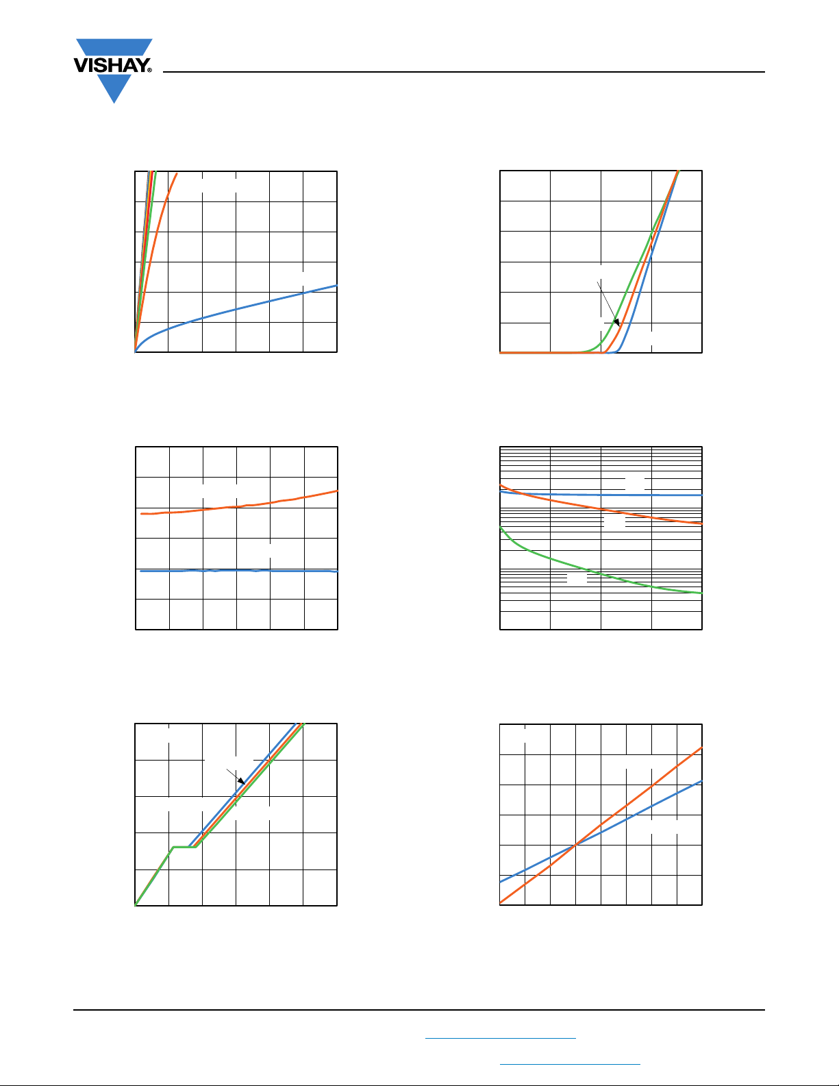
CHANNEL-1 TYPICAL CHARACTERISTICS (25 °C, unless otherwise noted)
SiZF906BDT
Vishay Siliconix
120
100
80
60
2nd line
40
- Drain Current (A)
D
I
20
0
0 0.51.01.52.02.53.0
VDS- Drain-to-Source Voltage (V)
Axis Title
VGS= 10 V thru 4 V
VGS= 3 V
10000
1000
100
10
1st line
2nd line
Output Characteristics
2nd line
2nd line
120
100
80
60
40
- Drain Current (A)
D
I
20
0
01234
VGS- Gate-to-Source Voltage (V)
Transfer Characteristics
10 000
1000
100
C - Capacitance (pF)
Axis Title
TC= 25 °C
TC= 125 °C
Axis Title
C
rss
C
oss
TC= -55 °C
C
iss
10000
1000
100
10
10000
1000
100
1st line
2nd line
1st line
2nd line
On-Resistance vs. Drain Current
10
ID= 20 A
8
6
2nd line
4
- Gate-to-Source Voltage (V)
2
GS
V
0
S20-0516-Rev. A, 29-Jun-2020
THIS DOCUMENT IS SUBJECT TO CHANGE WITHOUT NOTICE. THE PRODUCTS DESCRIBED HEREIN AND THIS DOCUMENT
VDS= 7.5 V
0 5 10 15 20 25 30
Qg- Total Gate Charge (nC)
Gate Charge
ARE SUBJECT TO SPECIFIC DISCLAIMERS, SET FORTH AT www.vishay.com/doc?91000
Axis Title
VDS= 15 V
VDS= 24 V
10
0 5 10 15 20
VDS- Drain-to-Source Voltage (V)
10000
1000
100
10
1st line
2nd line
ID= 15 A
On-Resistance vs. Junction Temperature
4
For technical questions, contact: pmostechsupport@vishay.com
10
Capacitance
Document Number: 77619
Page 5

10
100
1000
10000
0
0.0020
0.0040
0.0060
0.0080
0.0100
0246810
Axis Title
1st line
2nd line
2nd line
R
DS(on)
- On-Resistance (Ω)
VGS- Gate-to-Source Voltage (V)
TJ= 125 °C
TJ= 25 °C
10
100
1000
10000
0.01
0.1
1
10
100
1000
0.01 0.1 1 10 100
Axis Title
1st line
2nd line
2nd line
I
D
- Drain Current (A)
VDS- Drain-to-Source Voltage (V)
TA= 25 °C,
single pulse
Limited by R
DS(on)
a
BVDSS limited
100 ms, 10 ms
DC
1 ms, 100 μs
I
D(ON)
limited
1 s
10 s
www.vishay.com
CHANNEL-1 TYPICAL CHARACTERISTICS (25 °C, unless otherwise noted)
SiZF906BDT
Vishay Siliconix
TJ= 150 °C
Axis Title
Axis Title
TJ= 25 °C
ID= 250 μA
1
10000
1000
100
10
10000
1000
100
1st line
2nd line
On-Resistance vs. Gate-to-Source Voltage
50
40
30
1st line
2nd line
2nd line
20
P - Power (W )
Axis Title
10000
1000
100
1st line
2nd line
100
10
1
2nd line
- Source Current (A)
S
0.1
I
0.01
0 0.2 0.4 0.6 0.8
VSD- Source-to-Drain Voltage (V)
Source-Drain Diode Forward Voltage
2.0
1.8
(V)
1.6
GS(th)
2nd line
V
1.4
1.2
1.0
0.8
-50 -25 0 25 50 75 100 125 150
TJ- Junction Temperature (°C)
Threshold Voltage
Note
a. V
GS
S20-0516-Rev. A, 29-Jun-2020
> minimum VGS at which R
THIS DOCUMENT IS SUBJECT TO CHANGE WITHOUT NOTICE. THE PRODUCTS DESCRIBED HEREIN AND THIS DOCUMENT
ARE SUBJECT TO SPECIFIC DISCLAIMERS, SET FORTH AT www.vishay.com/doc?91000
10
10
0
0.001 0.01 0.1 1 10 100 1000
0.0001
Single Pulse Power, Junction-to-Ambient
IDMlimited
Safe Operating Area, Junction-to-Ambient
is specified
DS(on)
For technical questions, contact: pmostechsupport@vishay.com
5
10
t - Time (s)
Document Number: 77619
Page 6

www.vishay.com
CHANNEL-1 TYPICAL CHARACTERISTICS (25 °C, unless otherwise noted)
SiZF906BDT
Vishay Siliconix
120
100
80
60
2nd line
40
- Drain Current (A)
D
I
20
0
0 25 50 75 100 125 150
TC- Case Temperature (°C)
Axis Title
Current Derating
a
10000
1000
100
10
50
40
30
1st line
2nd line
2nd line
20
P - Power (W )
10
0
0255075100125150
Power, Junction-to-Case
Axis Title
10000
1000
100
10
TC- Case Temperature (°C)
Note
a. The power dissipation P
dissipation limit for cases where additional heatsinking is used. It is used to determine the current rating, when this rating falls below the
is based on TJ max. = 150 °C, using junction-to-case thermal resistance, and is more useful in settling the upper
D
package limit
1st line
2nd line
S20-0516-Rev. A, 29-Jun-2020
6
Document Number: 77619
For technical questions, contact: pmostechsupport@vishay.com
THIS DOCUMENT IS SUBJECT TO CHANGE WITHOUT NOTICE. THE PRODUCTS DESCRIBED HEREIN AND THIS DOCUMENT
ARE SUBJECT TO SPECIFIC DISCLAIMERS, SET FORTH AT www.vishay.com/doc?91000
Page 7

10
100
1000
10000
0.01
0.1
1
0.0001 0.001 0.01 0.1 1 10 100 1000
Axis Title
1st line
2nd line
Normalized Effective Transient
Thermal Impedance
Square Wave Pulse Duration (s)
0.2
0.02
0.05
0.1
Single pulse
P
DM
t
1
t
2
1. Duty cycle, D =
2. Per unit base = R
thJA
= 60 °C/W
3. T
JM-TA
= PDMZ
thJA
(t)
4. Surface mounted
t
1
t
2
Notes
10
100
1000
10000
0.1
1
0.0001 0.001 0.01 0.1 1
Axis Title
1st line
2nd line
Normalized Effective Transient
Thermal Impedance
Square Wave Pulse Duration (s)
0.2
0.05
0.1
Single pulse
www.vishay.com
CHANNEL-1 TYPICAL CHARACTERISTICS (25 °C, unless otherwise noted)
Duty cycle = 0.5
Normalized Thermal Transient Impedance, Junction-to-Ambient
SiZF906BDT
Vishay Siliconix
Duty cycle = 0.5
Normalized Thermal Transient Impedance, Junction-to-Case
S20-0516-Rev. A, 29-Jun-2020
For technical questions, contact: pmostechsupport@vishay.com
THIS DOCUMENT IS SUBJECT TO CHANGE WITHOUT NOTICE. THE PRODUCTS DESCRIBED HEREIN AND THIS DOCUMENT
ARE SUBJECT TO SPECIFIC DISCLAIMERS, SET FORTH AT www.vishay.com/doc?91000
7
Document Number: 77619
Page 8

10
100
1000
10000
0
20
40
60
80
100
120
0 0.5 1.0 1.5 2.0 2.5 3.0
Axis Title
1st line
2nd line
2nd line
I
D
- Drain Current (A)
VDS- Drain-to-Source Voltage (V)
VGS= 3 V
VGS= 10V thru 4 V
10
100
1000
10000
0.6
0.8
1.0
1.2
1.4
1.6
1.8
2.0
-50-250 255075100125150
Axis Title
1st line
2nd line
2nd line
R
DS(on)
- On-Resistance (Normalized)
TJ- Junction Temperature (°C)
VGS= 4.5 V
VGS= 10 V
www.vishay.com
CHANNEL-2 TYPICAL CHARACTERISTICS (25 °C, unless otherwise noted)
SiZF906BDT
Vishay Siliconix
2nd line
- On-Resistance (Ω)
R
0.0012
0.0010
0.0008
0.0006
DS(on)
0.0004
Output Characteristics
Axis Title
VGS= 4.5 V
VGS= 10 V
10000
1000
100
120
100
80
60
2nd line
40
- Drain Current (A)
D
I
20
0
01234
VGS- Gate-to-Source Voltage (V)
Axis Title
TC= 25 °C
TC= 125 °C
TC= -55 °C
10000
1000
100
10
1st line
2nd line
Transfer Characteristics
10 000
1st line
2nd line
1000
2nd line
C - Capacitance (pF)
Axis Title
C
iss
C
oss
C
rss
10000
1000
100
1st line
2nd line
0.0002
0 20406080100120
ID- Drain Current (A)
On-Resistance vs. Drain Current
10
ID= 20 A
8
6
2nd line
4
- Gate-to-Source Voltage (V)
2
GS
V
0
S20-0516-Rev. A, 29-Jun-2020
THIS DOCUMENT IS SUBJECT TO CHANGE WITHOUT NOTICE. THE PRODUCTS DESCRIBED HEREIN AND THIS DOCUMENT
VDS= 7.5 V
0 20406080100
Qg- Total Gate Charge (nC)
Axis Title
VDS= 15 V
VDS= 24 V
Gate Charge
For technical questions, contact: pmostechsupport@vishay.com
ARE SUBJECT TO SPECIFIC DISCLAIMERS, SET FORTH AT www.vishay.com/doc?91000
10
100
0 5 10 15 20 25 30
VDS- Drain-to-Source Voltage (V)
10
Capacitance
10000
1000
100
10
1st line
2nd line
ID= 15 A
On-Resistance vs. Junction Temperature
8
Document Number: 77619
Page 9

10
100
1000
10000
10
-8
10
-7
10
-6
10
-5
10
-4
10
-3
10
-2
10
-1
-50-250 255075100125150
Axis Title
1st line
2nd line
I
R
(A)
TJ- Junction Temperature (°C)
VDS= 30 V
VDS= 20 V
10
100
1000
10000
0.0000
0.0010
0.0020
0.0030
0.0040
0246810
Axis Title
1st line
2nd line
R
DS(on)
- On-Resistance (Ω)
VGS- Gate-to-Source Voltage (V)
TJ= 125 °C
TJ= 25 °C
10
100
1000
10000
0
10
20
30
40
0.0001
0.001 0.01 0.1 1 10 100 1000
Axis Title
1st line
2nd line
2nd line
P - Power (W )
t - Time (s)
10
100
1000
10000
0.01
0.1
1
10
100
1000
0.01 0.1 1 10 100
Axis Title
1st line
2nd line
2nd line
I
D
- Drain Current (A)
VDS- Drain-to-Source Voltage (V)
TA= 25 °C,
single pulse
Limited by R
DS(on)
a
BVDSS limited
1 ms, 100 μs
DC
I
D(ON)
limited
1 s
10 s
100 ms, 10 ms
www.vishay.com
CHANNEL-2 TYPICAL CHARACTERISTICS (25 °C, unless otherwise noted)
SiZF906BDT
Vishay Siliconix
100
TJ= 150 °C
10000
10
1000
Axis Title
TJ= 25 °C
1
1st line
2nd line
- Source Current (A)
S
0.1
I
0.01
100
10
2nd line
0 0.2 0.4 0.6 0.8 1.0
VSD- Source-to-Drain Voltage (V)
Source-Drain Diode Forward Voltage
On-Resistance vs. Gate-to-Source Voltage
Reverse Current (Schottky)
Note
a. V
GS
S20-0516-Rev. A, 29-Jun-2020
> minimum VGS at which R
THIS DOCUMENT IS SUBJECT TO CHANGE WITHOUT NOTICE. THE PRODUCTS DESCRIBED HEREIN AND THIS DOCUMENT
ARE SUBJECT TO SPECIFIC DISCLAIMERS, SET FORTH AT www.vishay.com/doc?91000
Single Pulse Power, Junction-to-Ambient
IDMlimited
Safe Operating Area, Junction-to-Ambient
is specified
DS(on)
For technical questions, contact: pmostechsupport@vishay.com
9
Document Number: 77619
Page 10

www.vishay.com
CHANNEL-2 TYPICAL CHARACTERISTICS (25 °C, unless otherwise noted)
SiZF906BDT
Vishay Siliconix
300
250
200
150
2nd line
100
- Drain Current (A)
D
I
50
0
0 25 50 75 100 125 150
TC- Case Temperature (°C)
Axis Title
Current Derating
a
10000
1000
100
10
100
80
60
1st line
2nd line
2nd line
40
P - Power (W )
20
0
0 25 50 75 100 125 150
Power, Junction-to-Case
Axis Title
10000
1000
100
10
TC- Case Temperature (°C)
Note
a. The power dissipation P
dissipation limit for cases where additional heatsinking is used. It is used to determine the current rating, when this rating falls below the
is based on TJ max. = 150 °C, using junction-to-case thermal resistance, and is more useful in settling the upper
D
package limit
1st line
2nd line
S20-0516-Rev. A, 29-Jun-2020
10
Document Number: 77619
For technical questions, contact: pmostechsupport@vishay.com
THIS DOCUMENT IS SUBJECT TO CHANGE WITHOUT NOTICE. THE PRODUCTS DESCRIBED HEREIN AND THIS DOCUMENT
ARE SUBJECT TO SPECIFIC DISCLAIMERS, SET FORTH AT www.vishay.com/doc?91000
Page 11

10
100
1000
10000
0.01
0.1
1
0.0001 0.001 0.01 0.1 1 10 100 1000
Axis Title
1st line
2nd line
Normalized Effective Transient
Thermal Impedance
Square Wave Pulse Duration (s)
0.2
0.02
0.05
0.1
Single pulse
P
DM
t
1
t
2
1. Duty cycle, D =
2. Per unit base = R
thJA
= 60 °C/W
3. T
JM-TA
= PDMZ
thJA
(t)
4. Surface mounted
t
1
t
2
Notes
10
100
1000
10000
0.1
1
0.0001 0.001 0.01 0.1 1
Axis Title
1st line
2nd line
Normalized Effective Transient
Thermal Impedance
Square Wave Pulse Duration (s)
0.2
0.05
0.1
Single pulse
www.vishay.com
CHANNEL-2 TYPICAL CHARACTERISTICS (25 °C, unless otherwise noted)
Duty cycle = 0.5
Normalized Thermal Transient Impedance, Junction-to-Ambient
SiZF906BDT
Vishay Siliconix
Duty cycle = 0.5
Normalized Thermal Transient Impedance, Junction-to-Case
Vishay Siliconix maintains worldwide manufacturing capability. Products may be manufactured at one of several qualified locations. Reliability data for Silicon
Technology and Package Reliability represent a composite of all qualified locations. For related documents such as package / tape drawings, part marking, and
reliability data, see www.vishay.com/ppg?77619
S20-0516-Rev. A, 29-Jun-2020
THIS DOCUMENT IS SUBJECT TO CHANGE WITHOUT NOTICE. THE PRODUCTS DESCRIBED HEREIN AND THIS DOCUMENT
ARE SUBJECT TO SPECIFIC DISCLAIMERS, SET FORTH AT www.vishay.com/doc?91000
.
For technical questions, contact: pmostechsupport@vishay.com
11
Document Number: 77619
Page 12

Legal Disclaimer Notice
www.vishay.com
Vishay
Disclaimer
ALL PRODUCT, PRODUCT SPECIFICATIONS AND DATA ARE SUBJECT TO CHANGE WITHOUT NOTICE TO IMPROVE
RELIABILITY, FUNCTION OR DESIGN OR OTHERWISE.
Vishay Intertechnology, Inc., its affiliates, agents, and employees, and all persons acting on its or their behalf (collectively,
“Vishay”), disclaim any and all liability for any errors, inaccuracies or incompleteness contained in any datasheet or in any other
disclosure relating to any product.
Vishay makes no warranty, representation or guarantee regarding the suitability of the products for any particular purpose or
the continuing production of any product. To the maximum extent permitted by applicable law, Vishay disclaims (i) any and all
liability arising out of the application or use of any product, (ii) any and all liability, including without limitation special,
consequential or incidental damages, and (iii) any and all implied warranties, including warranties of fitness for particular
purpose, non-infringement and merchantability.
Statements regarding the suitability of products for certain types of applications are based on Vishay’s knowledge of
typical requirements that are often placed on Vishay products in generic applications. Such statements are not binding
statements about the suitability of products for a particular application. It is the customer’s responsibility to validate that a
particular product with the properties described in the product specification is suitable for use in a particular application.
Parameters provided in datasheets and / or specifications may vary in different applications and performance may vary over
time. All operating parameters, including typical parameters, must be validated for each customer application by the customer’s
technical experts. Product specifications do not expand or otherwise modify Vishay’s terms and conditions of purchase,
including but not limited to the warranty expressed therein.
Except as expressly indicated in writing, Vishay products are not designed for use in medical, life-saving, or life-sustaining
applications or for any other application in which the failure of the Vishay product could result in personal injury or death.
Customers using or selling Vishay products not expressly indicated for use in such applications do so at their own risk.
Please contact authorized Vishay personnel to obtain written terms and conditions regarding products designed for
such applications.
No license, express or implied, by estoppel or otherwise, to any intellectual property rights is granted by this document
or by any conduct of Vishay. Product names and markings noted herein may be trademarks of their respective owners.
© 2021 VISHAY INTERTECHNOLOGY, INC. ALL RIGHTS RESERVED
Revision: 01-Jan-2021
1
Document Number: 91000
 Loading...