

PRODUCT SUMMARY
C/W
Si1553DL
Vishay Siliconix
Complementary 2.5-V (G-S) MOSFET
V
DS
N-Channel 20
P-Channel -20
(V) r
0.385 @ VGS = 4.5 V "0.70
0.630 @ VGS = 2.5 V "0.54
0.995 @ VGS = -4.5 V "0.44
1.800 @ VGS = -2.5 V "0.32
(W) I
DS(on)
(A)
D
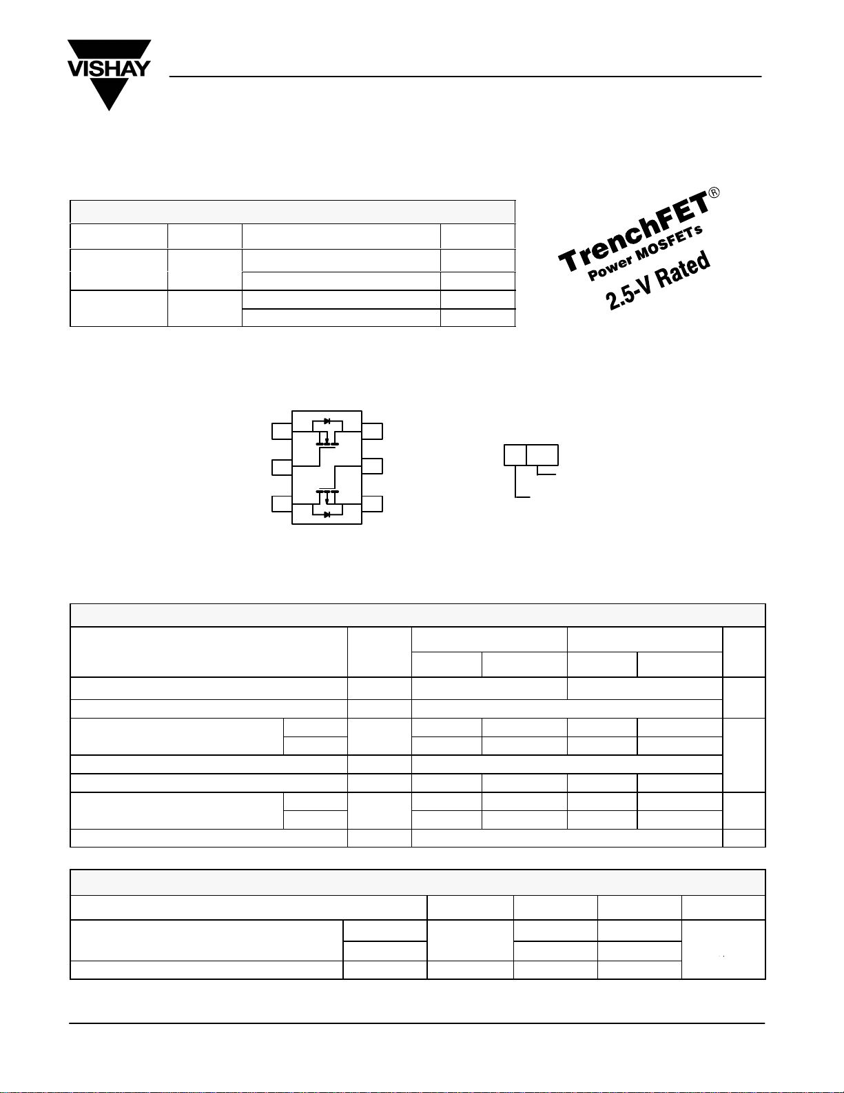
SOT-363
SC-70 (6-LEADS)
1
S
1
2
G
1
3
D
2
Top View
6
D
1
5
G
2
S
4
2
Marking Code
RA XX
Part # Code
YY
Lot Traceability
and Date Code
ABSOLUTE MAXIMUM RATINGS (TA = 25_C UNLESS OTHERWISE NOTED)
Parameter Symbol
Drain-Source Voltage V
Gate-Source Voltage V
a
Continuous Drain Current (TJ = 150_C)
Pulsed Drain Current I
Continuous Source Current (Diode Conduction)
Maximum Power Dissipation
Operating Junction and Storage Temperature Range TJ, T
_
a
TA = 25_C "0.70 "0.66 "0.44 "0.41
TA = 85_C
a
TA = 25_C 0.30 0.27 0.30 0.27
TA = 85_C
THERMAL RESISTANCE RATINGS
Parameter Symbol Typical Maximum Unit
Maximum Junction-to-Ambient
Maximum Junction-to-Foot (Drain) Steady State R
Notes
a. Surface Mounted on 1” x 1” FR4 Board.
Document Number: 71078
S-21374—Rev. D, 12-Aug-02
a
t v 5 sec 360 415
Steady State
N-Channel P-Channel
5 secs Steady State 5 secs Steady State
DS
GS
I
D
DM
I
S
P
D
stg
"0.50 "0.48 "0.31 "0.30
0.25 0.23 -0.25 -0.23
0.16 0.14 0.16 0.14
20 -20
"12
"1.0
-55 to 150 _C
R
thJA
thJF
400 460
300 350
Unit
V
A
W
_C/W
www.vishay.com
2-1
Si1553DL
W
^
W
Vishay Siliconix
SPECIFICATIONS (TJ = 25_C UNLESS OTHERWISE NOTED)
Parameter Symbol T est Condition Min Typ Max Unit
Static
Gate Threshold Voltage V
Gate-Body Leakage I
Zero Gate Voltage Drain Current I
On-State Drain Current
Drain-Source On-State Resistance
Forward Transconductance
Diode Forward Voltage
a
a
a
a
GS(th)
GSS
DSS
I
D(on)
r
DS(on)
g
V
fs
SD
Dynamicb
Total Gate Charge Q
Gate-Source Charge Q
Gate-Drain Charge Q
Turn-On Delay Time t
Rise Time t
Turn-Off Delay Time t
Fall Time t
Source-Drain
Source-Drain
Reverse Recovery Time
Notes
a. Pulse test; pulse width v
b. Guaranteed by design, not subject to production testing.
300 ms, duty cycle v 2%.
d(on)
d(off)
t
rr
g
gs
gd
r
f
VDS = VGS, I
VDS = VGS, I
VDS = 0 V, VGS = "12 V
= 250 mA N-Ch 0.6
D
= -250 mA P-Ch -0.6
D
N-Ch "100
P-Ch "100
VDS = 16 V, VGS = 0 V N-Ch 1
VDS = -16 V, VGS = 0 V P-Ch -1
VDS = 16 V, VGS = 0 V, TJ = 85_C N-Ch 5
VDS = -16 V, VGS = 0 V, TJ = 85_C P-Ch -5
VDS w 5 V, VGS = 4.5 V N-Ch 1.0
VDS p -5 V, VGS = -4.5 V P-Ch -1.0
VGS = 4.5 V, ID = 0.66 A N-Ch 0.320 0.385
VGS = -4.5 V, ID = -0.41 A P-Ch 0.850 0.995
VGS = 2.5 V, ID = 0.40 A N-Ch 0.560 0.630
VGS = -2.5 V, ID = -0.25 A P-Ch 1.4 1.800
VDS = 10 V, ID = 0.66 A N-Ch 1.5
VDS = -10 V, ID = -0.41 A P-Ch 0.8
IS = 0.23 A, VGS = 0 V N-Ch 0.8 1.2
IS = -0.23 A, VGS = 0 V P-Ch -0.8 -1.2
N-Ch 0.8 1.2
N-Channel
V
DS
V
= -10 V, VGS = -4.5 V, ID = -0.41 A
DS
N-Channel
= 10 V, VGS = 4.5 V, ID = 0.66 A
P-Channel
P-Ch 1.2 1.8
N-Ch 0.06
P-Ch 0.45
N-Ch 0.30
P-Ch 0.25
N-Ch 10 20
P-Ch 7.5 15
VDD = 10 V, RL = 20
ID ^ 0.5 A, V
V
= -10 V, RL = 20 W
DD
I ^ -0.5 A, V
I
-0.5 A, V
D
N-Channel
= 4.5 V, RG = 6 W
GEN
P-Channel
P-Channel
= -4.5 V, R = 6 W
= -4.5 V, RG = 6
GEN
N-Ch 16 30
P-Ch 20 40
N-Ch 10 20
P-Ch 8.5 17
N-Ch 10 20
P-Ch 12 24
IF = 0.23 A, di/dt = 100 A/ms N-Ch 20 40
IF = -0.23 A, di/dt = 100 A/ms P-Ch 25 40
V
nA
mA
A
W
S
V
nC
ns
www.vishay.com
2-2
Document Number: 71078
S-21374—Rev. D, 12-Aug-02
Si1553DL
Vishay Siliconix
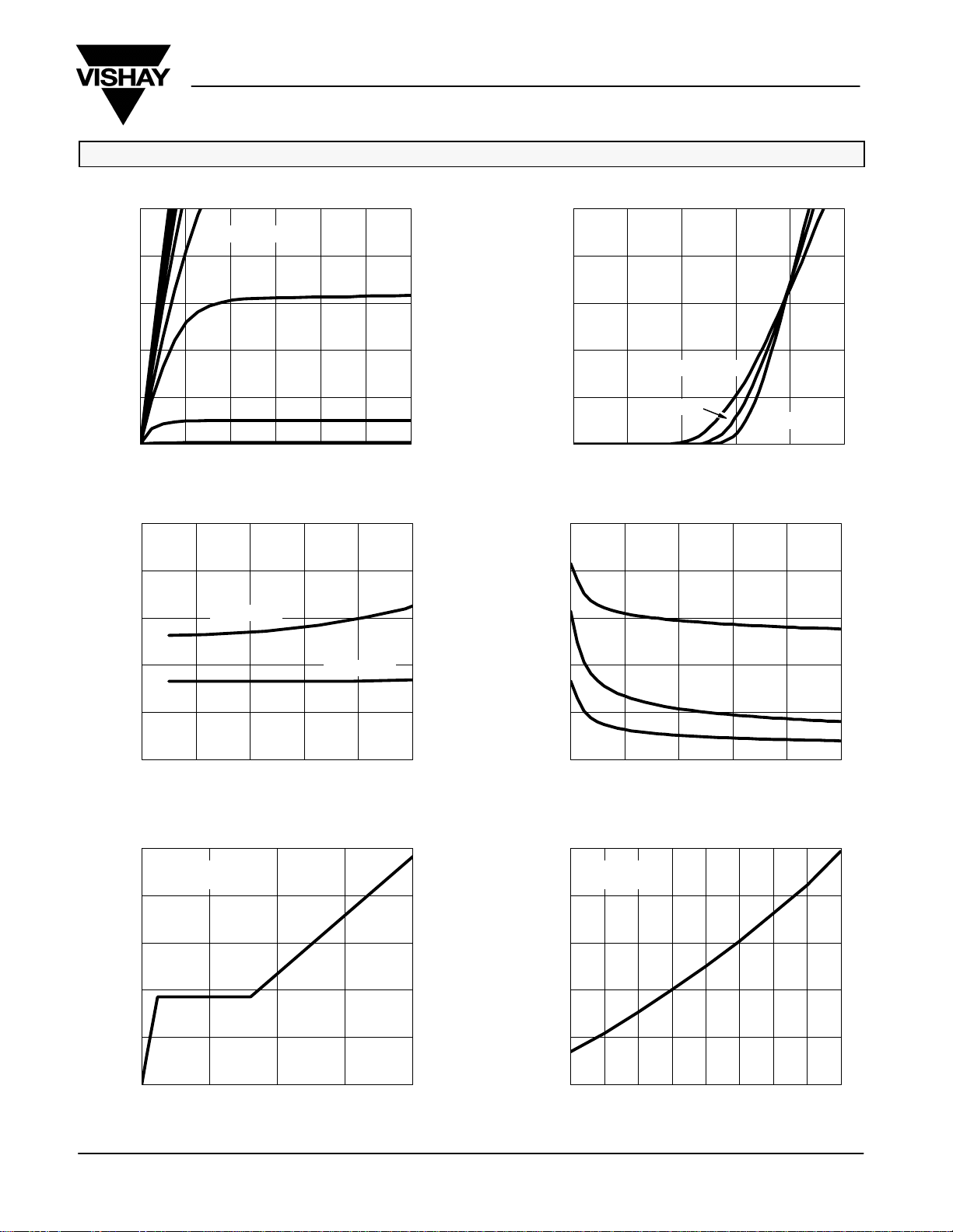
TYPICAL CHARACTERISTICS (25_C UNLESS NOTED) N−CHANNEL
1.0
VGS = 5 thru 2.5 V
0.8
0.6
0.4
- Drain Current (A)I
D
0.2
0.0
0.0 0.5 1.0 1.5 2.0 2.5 3.0
VDS - Drain-to-Source Voltage (V)
On-Resistance vs. Drain Current
1.0
W )
0.8
Output Characteristics Transfer Characteristics
0.6
VGS = 2.5 V
2 V
1.5 V
1 V
1.0
0.8
0.6
0.4
- Drain Current (A)I
D
0.2
0.0
0.0 0.5 1.0 1.5 2.0 2.5
VGS - Gate-to-Source Voltage (V)
TC = 125_C
25_C
Capacitance
100
80
C
60
iss
-55_C
- On-Resistance (r
0.4
DS(on)
0.2
0.0
0.0 0.2 0.4 0.6 0.8 1.0
- Drain Current (A)
I
D
Gate Charge
5
VDS = 10 V
I
= 0.66 A
D
4
3
2
- Gate-to-Source Voltage (V)
GS
1
V
0
0.0 0.2 0.4 0.6 0.8
Qg - Total Gate Charge (nC)
VGS = 4.5 V
40
C - Capacitance (pF)
20
C
0
048121620
C
oss
rss
VDS - Drain-to-Source Voltage (V)
On-Resistance vs. Junction Temperature
1.6
VGS = 4.5 V
I
= 0.66 A
W)
1.4
1.2
(Normalized)
- On-Resistance (r
1.0
DS(on)
0.8
0.6
D
-50 -25 0 25 50 75 100 125 150
T
- Junction Temperature (_C)
J
Document Number: 71078
S-21374—Rev. D, 12-Aug-02
www.vishay.com
2-3

Si1553DL
Vishay Siliconix
TYPICAL CHARACTERISTICS (25_C UNLESS NOTED) N−CHANNEL
Source-Drain Diode Forward Voltage On-Resistance vs. Gate-to-Source Voltage
1
1.0
0.8
W )
TJ = 150_C
- Source Current (A)I
S
0.1
0.0 0.2 0.4 0.6 0.8 1.0 1.2
VSD - Source-to-Drain Voltage (V) VGS - Gate-to-Source Voltage (V)
Threshold Voltage
0.2
0.1
ID = 250 mA
-0.0
-0.1
Variance (V)V
GS(th)
-0.2
-0.3
TJ = 25_C
0.6
0.4
- On-Resistance (r
DS(on)
0.2
0.0
5
4
3
Power (W)
2
1
ID = 0.66 A
012345
Single Pulse Power
-0.4
-50 -25 0 25 50 75 100 125 150
0.1
Thermal Impedance
Normalized Effective Transient
0.01
www.vishay.com
2-4
2
1
Duty Cycle = 0.5
0.2
0.1
0.05
0.02
-4
10
TJ - Temperature (_C)
Normalized Thermal Transient Impedance, Junction-to-Ambient
Single Pulse
-3
10
0
-3
10
10
-1
-2
1 100 6001010
Time (sec)
Notes:
P
DM
t
1
t
2
t
thJA
t
thJA
100
1
2
=400_C/W
(t)
1. Duty Cycle, D =
2. Per Unit Base = R
3. TJM - TA = PDMZ
4. Surface Mounted
-2
10
-1
1 10 60010
Square Wave Pulse Duration (sec)
Document Number: 71078
S-21374—Rev. D, 12-Aug-02

Si1553DL
Vishay Siliconix
TYPICAL CHARACTERISTICS (25_C UNLESS NOTED) N−CHANNEL
Normalized Thermal Transient Impedance, Junction-to-Foot
2
1
Duty Cycle = 0.5
0.2
0.1
0.1
Thermal Impedance
Normalized Effective Transient
0.05
0.02
-4
Single Pulse
-3
10
-2
10
Square Wave Pulse Duration (sec)
-1
11010
0.01
10
TYPICAL CHARACTERISTICS (25_C UNLESS NOTED) P−CHANNEL
1.0
VGS = 5 thru 3 V
0.8
0.6
0.4
- Drain Current (A)I
D
0.2
1 V
0.0
0.0 0.5 1.0 1.5 2.0 2.5 3.0
VDS - Drain-to-Source Voltage (V)
On-Resistance vs. Drain Current
3.0
Output Characteristics Transfer Characteristics
2.5 V
2 V
1.5 V
1.0
TC = -55_C
0.8
0.6
0.4
- Drain Current (A)I
D
0.2
0.0
0.0 0.5 1.0 1.5 2.0 2.5 3.0
VGS - Gate-to-Source Voltage (V)
25_C
Capacitance
100
125_C
W )
2.5
2.0
1.5
- On-Resistance (r
1.0
DS(on)
0.5
0.0
0.0 0.2 0.4 0.6 0.8 1.0
Document Number: 71078
S-21374—Rev. D, 12-Aug-02
VGS = 2.5 V
ID - Drain Current (A)
VGS = 3.6 V
VGS = 4.5 V
80
60
40
C - Capacitance (pF)
20
C
0
048121620
C
oss
rss
VDS - Drain-to-Source Voltage (V)
C
iss
www.vishay.com
2-5

Si1553DL
Vishay Siliconix
TYPICAL CHARACTERISTICS (25_C UNLESS NOTED) P−CHANNEL
Gate Charge
5
VDS = 10 V
= 0.41 A
I
D
4
3
2
- Gate-to-Source Voltage (V)
GS
1
V
0
0.0 0.2 0.4 0.6 0.8 1.0 1.2 1.4
Qg - Total Gate Charge (nC)
Source-Drain Diode Forward Voltage On-Resistance vs. Gate-to-Source Voltage
1
TJ = 150_C
On-Resistance vs. Junction Temperature
1.6
VGS = 4.5 V
= 0.41 A
I
W)
(Normalized)
- On-Resistance (r
DS(on)
3.0
2.5
W )
2.0
1.5
D
1.4
1.2
1.0
0.8
0.6
-50 -25 0 25 50 75 100 125 150
T
- Junction Temperature (_C)
J
ID = 0.41 A
- Source Current (A)I
S
0.1
0.0 0.2 0.4 0.6 0.8 1.0 1.2
VSD - Source-to-Drain Voltage (V) VGS - Gate-to-Source Voltage (V)
Threshold Voltage
0.4
0.3
ID = 250 mA
0.2
0.1
Variance (V)V
GS(th)
0.0
-0.1
-0.2
-50 -25 0 25 50 75 100 125 150
TJ - Temperature (_C)
TJ = 25_C
- On-Resistance (r
1.0
DS(on)
0.5
0.0
5
4
3
Power (W)
2
1
0
012345
Single Pulse Power
-1
-2
-3
10
10
1 100 6001010
Time (sec)
www.vishay.com
2-6
Document Number: 71078
S-21374—Rev. D, 12-Aug-02

Si1553DL
Vishay Siliconix
TYPICAL CHARACTERISTICS (25_C UNLESS NOTED) P−CHANNEL
Normalized Thermal Transient Impedance, Junction-to-Ambient
2
1
Duty Cycle = 0.5
0.2
Notes:
P
DM
t
1
t
1. Duty Cycle, D =
2. Per Unit Base = R
3. TJM - TA = PDMZ
4. Surface Mounted
2
thJA
t
t
thJA
100
1
2
(t)
= 400_C/W
0.1
Thermal Impedance
Normalized Effective Transient
0.01
10
2
-4
0.1
0.05
0.02
Single Pulse
-3
10
-2
10
-1
1 10 60010
Square Wave Pulse Duration (sec)
Normalized Thermal Transient Impedance, Junction-to-Foot
1
0.1
Thermal Impedance
Normalized Effective Transient
0.01
10
Duty Cycle = 0.5
0.2
0.1
0.05
0.02
Single Pulse
-4
-3
10
-2
10
-1
11010
Square Wave Pulse Duration (sec)
Document Number: 71078
S-21374—Rev. D, 12-Aug-02
www.vishay.com
2-7
 Loading...