

Si1469DH
P-Channel 20-V (G-S) MOSFET
PRODUCT SUMMARY
VDS (V) r
0.080 at V
- 20
0.155 at V
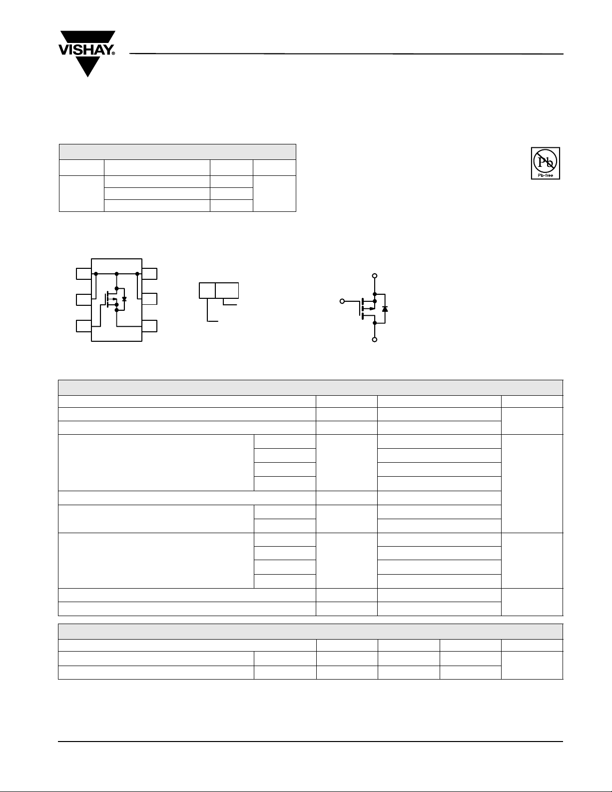
SOT-363
SC-70 (6-LEADS)
D
1
D
2
G
3
Top V i ew
Ordering Information: Si1469DH-T1-E3 (Lead (Pb)-free)
(Ω)
DS(on)
= - 10 V - 1.6
GS
= - 4.5 V - 1.6
GS
= - 2.5 V - 1.6
GS
D
6
5
D
S
4
Marking Code
BL XX
I
(A)
D
Par t #
Code
New Product
c
Qg (Typ)
5.5 nC0.100 at V
YY
Lot Traceability
and Date Code
FEATURES
• TrenchFET® Power MOSFET
APPLICATIONS
• Load Switch for Portable Devices
S
G
D
P-Channel MOSFET
Vishay Siliconix
RoHS
COMPLIANT
ABSOLUTE MAXIMUM RATINGS TA = 25 °C, unless otherwise noted
Parameter Symbol Limit Unit
Drain-Source Voltage
Gate-Source Voltage
Continuous Drain Current (T
= 150 °C)
J
a, b
Pulsed Drain Current (10 µs Pulse Width)
Continuous Source-Drain Diode Current
Maximum Power Dissipation
a, b
a, b
Operating Junction and Storage Temperature Range
Soldering Recommendations (Peak Temperature)
c, d
TC = 25 °C
T
= 70 °C
C
TA = 25 °C
TA = 70 °C
TC = 25 °C
TA = 25 °C
TC = 25 °C
= 70 °C
T
C
T
= 25 °C
A
TA = 70 °C
V
DS
V
GS
I
D
I
DM
I
S
P
D
, T
T
J
stg
- 20
± 12
c
-1.6
c
- 1.6
a, b, c
- 1.6
a, b, c
- 1.6
c
- 6.5
c
- 1.6
a, b, c
- 1.6
2.78
1.78
a, b
2.5
a, b
1
- 55 to 150
260
V
A
W
°C
THERMAL RESISTANCE RATINGS
Parameter Symbol Typical Maximum Unit
Maximum Junction-to-Ambient
a, d
t ≤ 5 sec
Maximum Junction-to-Foot (Drain) Steady State
Notes:
a. Surface Mounted on 1" x 1" FR4 board.
b. t = 5 sec.
c. Package limited.
d. Maximum under Steady State conditions is 125 °C/W.
R
thJA
R
thJF
60 80
34 45
°C/W
Document Number: 74441
S-70195-Rev. A, 29-Jan-07
www.vishay.com
1
Si1469DH
Vishay Siliconix
SPECIFICATIONS TJ = 25 °C, unless otherwise noted
Parameter Symbol Test Conditions Min Typ Max Unit
Static
Drain-Source Breakdown Voltage
V
Temperature Coefficient ΔVDS/T
DS
V
Temperature Coefficient ΔV
GS(th)
Gate-Source Threshold Voltage
Gate-Source Leakage
Zero Gate Voltage Drain Current
On-State Drain Current
Drain-Source On-State Resistance
Forward Transconductance
Dynamic
b
a
a
a
Input Capacitance
Reverse Transfer Capacitance
Total Gate Charge
V
DS
J
GS(th)/TJ
V
GS(th)
I
GSS
I
DSS
I
V
D(on)
r
DS(on)
g
fs
C
iss
C
oss
C
rss
Q
g
Qgs
Q
t
d(on)
t
d(off)
t
d(on)
t
d(off)
gd
R
g
t
r
t
f
t
r
t
f
Gate-Drain Charge
Gate Resistance
Tur n - On D e l a y T im e
Rise Time
Turn-Off Delay Time
Fall Time
Tur n - On D e l a y T im e
Rise Time
Turn-Off Delay Time
Fall Time
Drain-Source Body Diode Characteristics
Continuous Source-Drain Diode Current
Pulse Diode Forward Current
Body Diode Voltage
Body Diode Reverse Recovery Time
Body Diode Reverse Recovery Charge
Reverse Recovery Fall Time
Reverse Recovery Rise Time
I
S
I
SM
V
SD
t
rr
Q
rr
t
a
t
b
Notes:
a. Pulse test; pulse width ≤ 300 µs, duty cycle ≤ 2 %.
b. Guaranteed by design, not subject to production testing.
Stresses beyond those listed under “Absolute Maximum Ratings” may cause permanent damage to the device. These are stress ratings only, and functional operation
of the device at these or any other conditions beyond those indicated in the operational sections of the specifications is not implied. Exposure to absolute maximum
rating conditions for extended periods may affect device reliability.
VGS = 0 V, ID = - 250 µA
ID = - 250 µA
V
= VGS, ID = - 250 µA
DS
VDS = 0 V, VGS = ± 12 V
V
V
DS
= - 20 V, V
DS
= - 20 V, V
V
GS
V
GS
V
GS
GS
≤ 5 V, V
DS
= - 10 V, ID = - 2.0 A
= - 4.5 V, ID = - 1.8 A
= - 2.5 V, ID = - 1.5 A
= 0 V
GS
= 0 V, TJ = 55 °C
= - 4.5 V
GS
VDS = - 10 V, ID = - 2.0 A
VDS = - 10 V, V
VDS = - 10 V, V
= 0 V, f = 1 MHz
GS
= - 4.5 V, ID = - 2.5 A
GS
f = 1 MHz 10 Ω
V
= - 10 V, RL = 5 Ω
DD
≅ - 2 A, V
I
D
≅ - 2 A, V
I
D
V
= - 4.5 V, Rg = 1 Ω
GEN
= - 10 V, RL = 5 Ω
DD
= - 10 V, Rg = 1 Ω
GEN
TC = 25 °C
IS = - 2 A, V
GS
= 0 V
IF = - 2.0 A, di/dt = 100 A/µs, TJ = 25 °C
- 20 V
- 21
- 2.4
mV/°C
- 0.6 - 1.5 V
- 100 nA
- 1
- 10
µA
- 3 A
0.065 0.080
0.081 0.100
0.126 0.155
6S
470
105
80
5.5 8.5
0.8
nCGate-Source Charge
1.7
27 41
48 72
27 41
15 23
510
20 30
22 33
918
- 1.6
- 6.5
- 0.83 - 1.2 V
20 30 ns
815nC
7
13
Ω
pFOutput Capacitance
ns
A
ns
www.vishay.com
2
Document Number: 74441
S-70195-Rev. A, 29-Jan-07
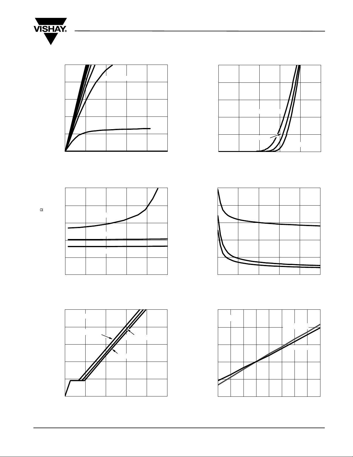
TYPICAL CHARACTERISTICS 25 °C, unless otherwise noted
Si1469DH
Vishay Siliconix
10
8
6
4
- Drain Current (A)I
D
2
0
0.0 0.6 1.2 1.8 2.4 3.0
VDS - Drain-to-Source Voltage (V)
VGS = 10 thru 3 V
2 V
Output Characteristics
0.20
0.16
)
VGS = 2.5 V
0.12
2.5
2.0
1.5
T
C
TC = 125 °C
= 25 °C
T
C
1.0
- Drain Current (A)I
D
0.5
0.0
0.0 0.5 1.0 1.5 2.0 2.5
VGS - Gate-to-Source Voltage (V)
Transfer Characteristics
800
640
C
iss
480
= - 55 °C
- On-Resistance (r
VGS = 4.5 V
0.0
8
DS(on)
0.04
0.00
0.0 1.4 2.8 4.2 5.6 7.0
VGS = 10 V
ID - Drain Current (A)
On-Resistance vs. Drain Current and Gate Voltage
10
ID = 2.5 A
8
6
4
- Gate-to-Source Voltage (V)V
GS
2
0
0 3 6 9 12 15
VDS = 5 V
VDS = 10 V
VDS = 15 V
Qg - Total Gate Charge (nC)
Gate Charge
C - Capacitance (pF)
- On-Resistance
(Normalized)
DS(on)
r
320
C
160
C
rss
0
048 12 16 20
oss
VDS - Drain-to-Source Voltage (V)
Capacitance
1.6
ID = 2 A
1.4
1.2
1.0
0.8
0.6
- 50 - 25 0 25 50 75 100 125 150
TJ- Junction Temperature (°C)
VGS = 2.5 V
VGS = 10 V
On-Resistance vs. Junction Temperature
Document Number: 74441
S-70195-Rev. A, 29-Jan-07
www.vishay.com
3

Si1469DH
Vishay Siliconix
TYPICAL CHARACTERISTICS 25 °C, unless otherwise noted
- Source Current (A)I
S
10
T
= 150 °C
1
0.1
0.01
0.0 0.3 0.6 0.9 1.2 1.5
J
TJ = 25 °C
VSD - Source-to-Drain Voltage (V)
Source-Drain Diode Forward Voltage
0.4
0.
3
0.2
0.1
Variance (V)
GS(th)
0.0
V
- 0.1
ID = 5 mA
ID = 250 µA
0.5
ID = 2 A
0.4
)
0.3
0.2
- On-Resistance (r
DS(on)
0.1
25 °C
0.0
02468 10
V
GS
125 °C
- Gate-to-Source Voltage (V)
On-Resistance vs. Gate-to-Source Voltage
30
24
8
1
12
Power (W)
6
- 0.2
- 50 - 25 0 25 50 75 100 125 150
www.vishay.com
4
TJ - Temperature (°C)
Threshold Voltage
- Drain Current (A)I
D
10
Limited by r
1
0.1
0.01
0.01
*V
DS(on)
TC = 25 °C
Single Pulse
0.1
VDS - Drain-to-Source Voltage (V)
minimum VGS at which r
GS
1
Safe Operating Area, Junction-to-Ambient
0
10 100
isspecified
DS(on)
0.1
Time (sec)
Single Pulse Power, Junction-to-Ambient
1 ms
10 ms
100 ms
1 s
10 s
dc
Document Number: 74441
S-70195-Rev. A, 29-Jan-07
011100.0 0.01

TYPICAL CHARACTERISTICS 25 °C, unless otherwise noted
5
Si1469DH
Vishay Siliconix
3.5
4
3
2
- Drain Current (A)
D
I
1
0
0 25 50 75 100 125 150
Package Limited
TC - Case Temperature (°C)
Current Derating*
1.20
0.96
0.72
0.48
Power Dissipation (W)
0.24
2.8
2.1
1.4
Power Dissipation (W)
0.7
0.0
0 25 50 75 100 125 150
TC - Case Temperature (°C)
Power Derating, Junction-to-Foot
0.00
0 25 50 75 100 125 150
TA - Ambient Temperature (°C)
Power Derating, Junction-to-Ambient
*The power dissipation PD is based on T
= 175 °C, using junction-to-case thermal resistance, and is more useful in settling the upper dis-
J(max)
sipation limit for cases where additional heatsinking is used. It is used to determine the current rating, when this rating falls below the package
limit.
Document Number: 74441
www.vishay.com
S-70195-Rev. A, 29-Jan-07
5

Si1469DH
Vishay Siliconix
TYPICAL CHARACTERISTICS 25 °C, unless otherwise noted
1
Duty Cycle = 0.5
Normalized Effective Transient
Normalized Effective Transient
Thermal Impedance
Thermal Impedance
0.1
0.01
10
1
0.1
0.01
10
0.2
0.1
0.05
0.02
Single Pulse
-4
Duty Cycle = 0.5
0.2
0.1
0.02
Single Pulse
-4
Notes:
P
DM
t
1
t
2
t
thJA
100
1
t
2
= 125 °C/W
thJA
(t)
100010
1. Duty Cycle, D =
2. Per Unit Base = R
3. T
- TA = PDMZ
JM
4. Surface Mounted
-3
10
-2
10
-1
1
10
Square Wave Pulse Duration (sec)
Normalized Thermal Transient Impedance, Junction-to-Ambient
0.05
-3
10
-2
10
-1
01110
Square Wave Pulse Duration (sec)
Normalized Thermal Transient Impedance, Junction-to-Foot
Vishay Siliconix maintains worldwide manufacturing capability. Products may be manufactured at one of several qualified locations. Reliability data for Silicon Technology and Package Reliability represent a composite of all qualified locations. For related documents such as package/tape drawings, part marking, and reliability
data, see http://www.vishay.com/ppg?74441.
www.vishay.com
6
Document Number: 74441
S-70195-Rev. A, 29-Jan-07

Legal Disclaimer Notice
Vishay
Notice
Specifications of the products displayed herein are subject to change without notice. Vishay Intertechnology, Inc.,
or anyone on its behalf, assumes no responsibility or liability for any errors or inaccuracies.
Information contained herein is intended to provide a product description only. No license, express or implied, by
estoppel or otherwise, to any intellectual property rights is granted by this document. Except as provided in Vishay's
terms and conditions of sale for such products, Vishay assumes no liability whatsoever, and disclaims any express
or implied warranty, relating to sale and/or use of Vishay products including liability or warranties relating to fitness
for a particular purpose, merchantability, or infringement of any patent, copyright, or other intellectual property right.
The products shown herein are not designed for use in medical, life-saving, or life-sustaining applications.
Customers using or selling these products for use in such applications do so at their own risk and agree to fully
indemnify Vishay for any damages resulting from such improper use or sale.
Document Number: 91000 www.vishay.com
Revision: 08-Apr-05 1

 Loading...