

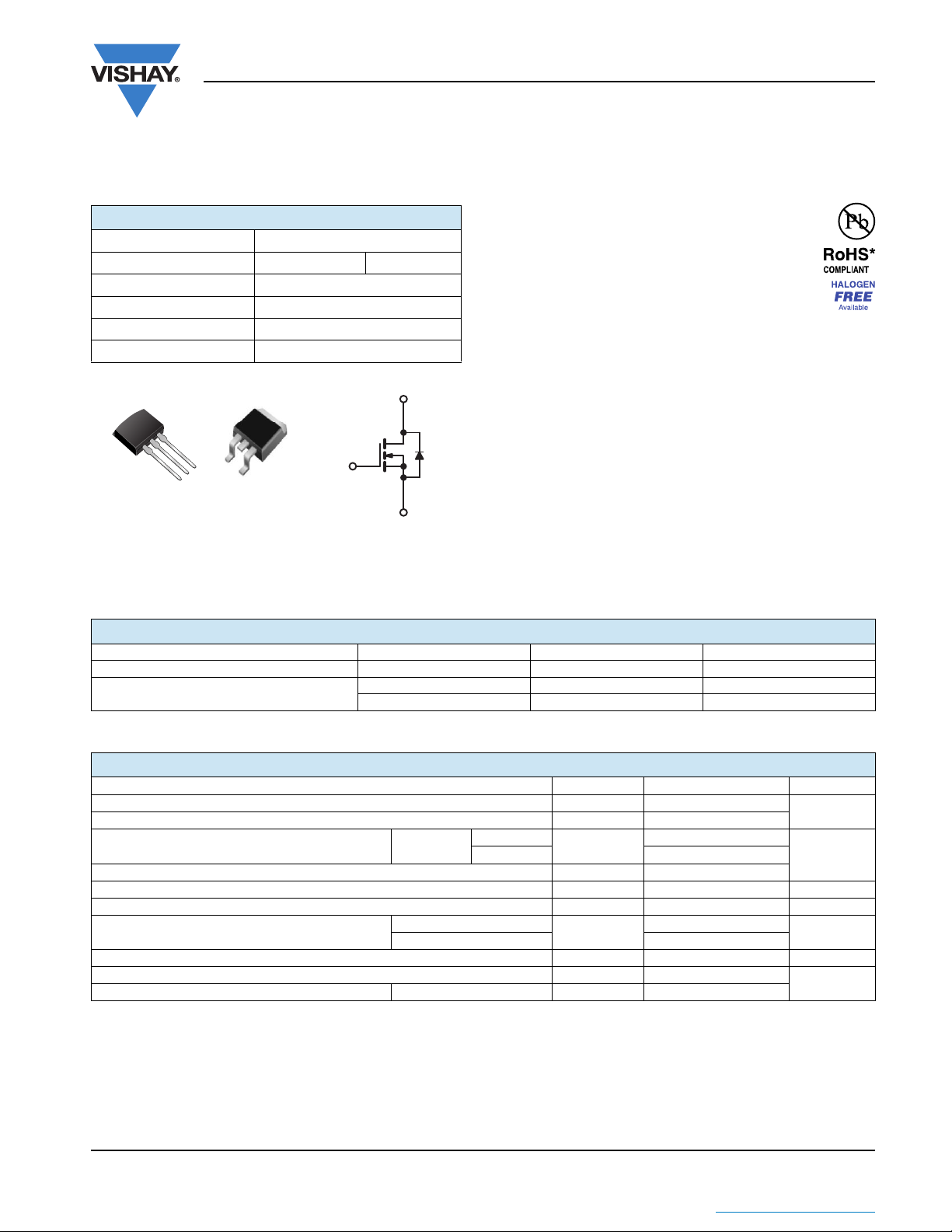
N-Channel MOSFET
G
D
S
D2PAK (TO-263)
G
D
S
I2PAK (TO-262)
G
D
S
IRFZ24S, IRFZ24L, SiHFZ24S, SiHFZ24S
Vishay Siliconix
Power MOSFET
PRODUCT SUMMARY
VDS (V) 60
()V
R
DS(on)
Q
(Max.) (nC) 25
g
Q
(nC) 5.8
gs
Q
(nC) 11
gd
Configuration Single
= 10 V 0.10
GS
FEATURES
• Halogen-free According to IEC 61249-2-21
Definition
• Advanced Process Technology
• Surface Mount (IRFZ24S, SiHFZ24S)
• Low-ProfileThrough-Hole (IRFZ24L, SiHFZ24L)
• 175 °C Operating Temperature
•Fast Switching
• Compliant to RoHS Directive 2002/95/EC
DESCRIPTION
Third generation Power MOSFETs from Vishay utilize
advanced processing techniques to achieve extremely low
on-resistance per silicon area. This benefit, combined with
the fast switching speed and ruggedized device design that
Power MOSFETs are well known for, provides the designer
with an extremely efficient and reliable device for use in a
wide variety of applications.
The D2PAK is a surface mount power package capable of
accommodating die size up to HEX-4. It provides the highest
power capability and the last lowest possible on-resistance
in any existing surface mount package. The D
suitable for high current applications because of its low
internal connection resistance and can dissipate up to 2.0 W
in a typical surface mount application. The through-hole
version (IRFZ24L, SiHFZ24L) is available for low-profile
applications.
ORDERING INFORMATION
Package
Lead (Pb)-free and Halogen-free SiHFZ24S-GE3 SiHFZ24STRR-GE3 -
Lead (Pb)-free
Note
a. See device orientation.
2
D
PAK (TO-263) D2PAK (TO-263) I2PAK (TO-262)
IRFZ24SPbF - IRFZ24LPbF
SiHFZ24S-E3 - SiHFZ24L-E3
2
PAK is
ABSOLUTE MAXIMUM RATINGS (TC = 25 °C, unless otherwise noted)
PARAMETER SYMBOL LIMIT UNIT
Drain-Source Voltage V
Gate-Source Voltage V
T
= 25 °C
Continuous Drain Current V
Pulsed Drain Current
Linear Derating Factor 0.40 W/°C
Single Pulse Avalanche Energy
Maximum Power Dissipation
Peak Diode Recovery dV/dt
Operating Junction and Storage Temperature Range T
Soldering Recommendations (Peak Temperature) for 10 s 300
Notes
a. Repetitive rating; pulse width limited by maximum junction temperature (see fig. 11).
b. V
= 25 V, starting TJ = 25 °C, L = 400 μH, Rg = 25 , IAS = 17 A (see fig. 12).
DD
17 A, dI/dt 140 A/μs, VDD VDS, TJ 175 °C.
c. I
SD
d. 1.6 mm from case.
e. Uses IRFZ24, SiHFZ24 data and test conditions.
* Pb containing terminations are not RoHS compliant, exemptions may apply
Document Number: 90366
S11-1063-Rev. C, 30-May-11 1
THE PRODUCTS DESCRIBED HEREIN AND THIS DOCUMENT ARE SUBJECT TO SPECIFIC DISCLAIMERS, SET FORTH AT
a, e
b, e
c, e
This document is subject to change without notice.
at 10 V
GS
C
= 100 °C 12
T
C
T
= 25 °C
C
= 25 °C 3.7
T
A
www.vishay.com
DS
± 20
GS
I
D
IDM 68
E
AS
P
D
dV/dt 4.5 V/ns
, T
J
stg
60
17
100 mJ
60
- 55 to + 175
d
www.vishay.com/doc?91000
V
A
W
°C
IRFZ24S, IRFZ24L, SiHFZ24S, SiHFZ24S
Vishay Siliconix
THERMAL RESISTANCE RATINGS
PARAMETER SYMBOL TYP. MAX. UNIT
Maximum Junction-to-Ambient
(PCB Mounted, Steady-State)
a
Maximum Junction-to-Case (Drain) R
Note
a. When mounted on 1" square PCB (FR-4 or G-10 material).
SPECIFICATIONS (TJ = 25 °C, unless otherwise noted)
PARAMETER SYMBOL TEST CONDITIONS MIN. TYP. MAX. UNIT
Static
Drain-Source Breakdown Voltage V
V
Temperature Coefficient VDS/TJ Reference to 25 °C, ID = 1 mA
DS
Gate-Source Threshold Voltage V
Gate-Source Leakage I
Zero Gate Voltage Drain Current I
Drain-Source On-State Resistance R
Forward Transconductance g
Dynamic
Input Capacitance C
Reverse Transfer Capacitance C
Total Gate Charge Q
Gate-Drain Charge Q
Turn-On Delay Time t
Rise Time t
Turn-Off Delay Time t
Fall Time t
Internal Source Inductance L
Drain-Source Body Diode Characteristics
Continuous Source-Drain Diode Current I
Pulsed Diode Forward Current
Body Diode Voltage V
Body Diode Reverse Recovery Time t
Body Diode Reverse Recovery Charge Q
Forward Turn-On Time t
Notes
a. Repetitive rating; pulse width limited by maximum junction temperature (see fig. 11).
b. Pulse width 300 μs; duty cycle 2 %.
c. Uses IRFZ24/SiHFZ24 data and test conditions.
a
R
thJA
thJC
DS
GS(th)
V
GSS
-40
°C/W
-2.5
VGS = 0, ID = 250 μA 60 - - V
c
- 0.061 - V/°C
VDS = VGS, ID = 250 μA 2.0 - 4.0 V
= ± 20 V - - ± 100 nA
GS
VDS = 60 V, VGS = 0 V - - 25
DSS
VGS = 10 V ID = 10 A
DS(on)
fs
iss
- 360 -
oss
-79-
rss
g
--5.8
gs
--11
gd
d(on)
r
-25-
d(off)
-42-
f
S
S
I
SM
SD
rr
rr
on
V
= 48 V, VGS = 0 V, TJ = 150 °C - - 250
DS
VDS = 25 V, ID = 10 A
VGS = 0 V,
V
= 25 V,
DS
f = 1.0 MHz, see fig. 5
b
d
d
- - 0.10
5.5 - - S
- 640 -
--25
= 17 A, VDS = 48 V,
I
V
GS
= 10 V
D
see fig. 6 and 13
b, c
-13-
V
= 30 V, ID = 17 A,
R
DD
= 18 , RD = 1.7 , see fig. 10
g
b, c
-58-
Between lead, and center of die contact - 7.5 - nH
MOSFET symbol
showing the
integral reverse
p - n junction diode
TJ = 25 °C, IS = 17 A, VGS = 0 V
TJ = 25 °C, IF = 17 A, dI/dt = 100 A/μs
D
G
S
b
b, c
--17
--68
--1.5V
- 88 180 ns
- 290 640 μC
Intrinsic turn-on time is negligible (turn-on is dominated by LS and LD)
μA
pFOutput Capacitance C
nC Gate-Source Charge Q
ns
A
www.vishay.com Document Number: 90366
2 S11-1063-Rev. C, 30-May-11
This document is subject to change without notice.
THE PRODUCTS DESCRIBED HEREIN AND THIS DOCUMENT ARE SUBJECT TO SPECIFIC DISCLAIMERS, SET FORTH AT
www.vishay.com/doc?91000
IRFZ24S, IRFZ24L, SiHFZ24S, SiHFZ24S
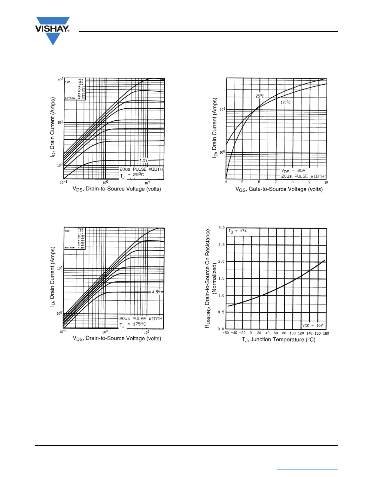
TYPICAL CHARACTERISTICS (25 °C, unless otherwise noted)
Vishay Siliconix
Fig. 1 - Typical Output Characteristics, TC = 25 °C
Fig. 2 - Typical Output Characteristics, T
= 175 °C
C
Fig. 3 - Typical Transfer Characteristics
Fig. 4 - Normalized On-Resistance vs. Temperature
Document Number: 90366 www.vishay.com
S11-1063-Rev. C, 30-May-11 3
THE PRODUCTS DESCRIBED HEREIN AND THIS DOCUMENT ARE SUBJECT TO SPECIFIC DISCLAIMERS, SET FORTH AT
This document is subject to change without notice.
www.vishay.com/doc?91000

IRFZ24S, IRFZ24L, SiHFZ24S, SiHFZ24S
Vishay Siliconix
Fig. 5 - Typical Capacitance vs. Drain-to-Source Voltage
Fig. 6 - Typical Gate Charge vs. Gate-to-Source Voltage
Fig. 7 - Typical Source-Drain Diode Forward Voltage
Fig. 8 - Maximum Safe Operating Area
www.vishay.com Document Number: 90366
4 S11-1063-Rev. C, 30-May-11
THE PRODUCTS DESCRIBED HEREIN AND THIS DOCUMENT ARE SUBJECT TO SPECIFIC DISCLAIMERS, SET FORTH AT
This document is subject to change without notice.
www.vishay.com/doc?91000

V
DS
90 %
10 %
V
GS
t
d(on)
t
r
t
d(off)
t
f
R
g
I
AS
0.01 W
t
p
D.U.T.
L
V
DS
+
-
V
DD
10 V
Var y t
p
to obtain
required I
AS
I
AS
V
DS
V
DD
V
DS
t
p
IRFZ24S, IRFZ24L, SiHFZ24S, SiHFZ24S
Vishay Siliconix
R
D.U.T.
D
+
V
-
DD
V
DS
V
GS
R
g
10 V
Pulse width ≤ 1 µs
Duty factor ≤ 0.1 %
Fig. 10a - Switching Time Test Circuit
Fig. 9 - Maximum Drain Current vs. Case Temperature
Fig. 11 - Maximum Effective Transient Thermal Impedance, Junction-to-Case
Fig. 10b - Switching Time Waveforms
Document Number: 90366 www.vishay.com
S11-1063-Rev. C, 30-May-11 5
THE PRODUCTS DESCRIBED HEREIN AND THIS DOCUMENT ARE SUBJECT TO SPECIFIC DISCLAIMERS, SET FORTH AT
Fig. 12a - Unclamped Inductive Test Circuit
Fig. 12b - Unclamped Inductive Waveforms
This document is subject to change without notice.
www.vishay.com/doc?91000

D.U.T.
3 mA
V
GS
V
DS
I
G
I
D
0.3 µF
0.2 µF
50 kΩ
12 V
Current regulator
Current sampling resistors
Same type as D.U.T.
+
-
IRFZ24S, IRFZ24L, SiHFZ24S, SiHFZ24S
Vishay Siliconix
Fig. 12c - Maximum Avalanche Energy vs. Drain Current
Q
10 V
V
Q
GS
G
G
Q
GD
Charge
Fig. 13a - Basic Gate Charge Waveform Fig. 13b - Gate Charge Test Circuit
www.vishay.com Document Number: 90366
6 S11-1063-Rev. C, 30-May-11
This document is subject to change without notice.
THE PRODUCTS DESCRIBED HEREIN AND THIS DOCUMENT ARE SUBJECT TO SPECIFIC DISCLAIMERS, SET FORTH AT
www.vishay.com/doc?91000

IRFZ24S, IRFZ24L, SiHFZ24S, SiHFZ24S
Vishay Siliconix
Peak Diode Recovery dV/dt Test Circuit
D.U.T.
+
-
R
g
Driver gate drive
P.W.
+
-
Period
Circuit layout considerations
• Low stray inductance
• Ground plane
• Low leakage inductance
current transformer
• dV/dt controlled by R
• Driver same type as D.U.T.
I
controlled by duty factor “D”
•
SD
• D.U.T. - device under test
-
D =
g
Period
P.W.
+
+
V
DD
-
= 10 Va
V
GS
D.U.T. l
Reverse
recovery
current
D.U.T. V
Re-applied
voltage
Inductor current
Note
a. V
waveform
SD
Body diode forward
waveform
DS
Body diode forward drop
Ripple ≤ 5 %
= 5 V for logic level devices
GS
current
dI/dt
Diode recovery
dV/dt
V
DD
I
SD
Fig. 14 - For N-Channel
Vishay Siliconix maintains worldwide manufacturing capability. Products may be manufactured at one of several qualified locations. Reliability data for Silicon
Technology and Package Reliability represent a composite of all qualified locations. For related documents such as package/tape drawings, part marking, and
reliability data, see www.vishay.com/ppg?90366
.
Document Number: 90366 www.vishay.com
S11-1063-Rev. C, 30-May-11 7
This document is subject to change without notice.
THE PRODUCTS DESCRIBED HEREIN AND THIS DOCUMENT ARE SUBJECT TO SPECIFIC DISCLAIMERS, SET FORTH AT
www.vishay.com/doc?91000

www.vishay.com
M
*
3
2
1
L
L(1)
D
H(1)
Q
Ø P
A
F
J(1)
b(1)
e(1)
e
E
b
C
Package Information
Vishay Siliconix
TO-220AB
MILLIMETERS INCHES
DIM. MIN. MAX. MIN. MAX.
A 4.25 4.65 0.167 0.183
b 0.69 1.01 0.027 0.040
b(1) 1.20 1.73 0.047 0.068
c 0.36 0.61 0.014 0.024
D 14.85 15.49 0.585 0.610
E 10.04 10.51 0.395 0.414
e 2.41 2.67 0.095 0.105
e(1) 4.88 5.28 0.192 0.208
F 1.14 1.40 0.045 0.055
H(1) 6.09 6.48 0.240 0.255
J(1) 2.41 2.92 0.095 0.115
L 13.35 14.02 0.526 0.552
L(1) 3.32 3.82 0.131 0.150
Ø P 3.54 3.94 0.139 0.155
Q 2.60 3.00 0.102 0.118
ECN: T13-0724-Rev. O, 14-Oct-13
DWG: 5471
Note
* M = 1.32 mm to 1.62 mm (dimension including protrusion)
Heatsink hole for HVM
ARE SUBJECT TO SPECIFIC DISCLAIMERS, SET FORTH AT www.vishay.com/doc?91000
Revison: 14-Oct-13
THIS DOCUMENT IS SUBJECT TO CHANGE WITHOUT NOTICE. THE PRODUCTS DESCRIBED HEREIN AND THIS DOCUMENT
For technical questions, contact: hvm@vishay.com
1
Document Number: 71195

Legal Disclaimer Notice
www.vishay.com
Vishay
Disclaimer
ALL PRODUCT, PRODUCT SPECIFICATIONS AND DATA ARE SUBJECT TO CHANGE WITHOUT NOTICE TO IMPROVE
RELIABILITY, FUNCTION OR DESIGN OR OTHERWISE.
Vishay Intertechnology, Inc., its affiliates, agents, and employees, and all persons acting on its or their behalf (collectively,
“Vishay”), disclaim any and all liability for any errors, inaccuracies or incompleteness contained in any datasheet or in any other
disclosure relating to any product.
Vishay makes no warranty, representation or guarantee regarding the suitability of the products for any particular purpose or
the continuing production of any product. To the maximum extent permitted by applicable law, Vishay disclaims (i) any and all
liability arising out of the application or use of any product, (ii) any and all liability, including without limitation special,
consequential or incidental damages, and (iii) any and all implied warranties, including warranties of fitness for particular
purpose, non-infringement and merchantability.
Statements regarding the suitability of products for certain types of applications are based on Vishay’s knowledge of typical
requirements that are often placed on Vishay products in generic applications. Such statements are not binding statements
about the suitability of products for a particular application. It is the customer’s responsibility to validate that a particular
product with the properties described in the product specification is suitable for use in a particular application. Parameters
provided in datasheets and/or specifications may vary in different applications and performance may vary over time. All
operating parameters, including typical parameters, must be validated for each customer application by the customer’s
technical experts. Product specifications do not expand or otherwise modify Vishay’s terms and conditions of purchase,
including but not limited to the warranty expressed therein.
Except as expressly indicated in writing, Vishay products are not designed for use in medical, life-saving, or life-sustaining
applications or for any other application in which the failure of the Vishay product could result in personal injury or death.
Customers using or selling Vishay products not expressly indicated for use in such applications do so at their own risk. Please
contact authorized Vishay personnel to obtain written terms and conditions regarding products designed for such applications.
No license, express or implied, by estoppel or otherwise, to any intellectual property rights is granted by this document or by
any conduct of Vishay. Product names and markings noted herein may be trademarks of their respective owners.
Material Category Policy
Vishay Intertechnology, Inc. hereby certifies that all its products that are identified as RoHS-Compliant fulfill the
definitions and restrictions defined under Directive 2011/65/EU of The European Parliament and of the Council
of June 8, 2011 on the restriction of the use of certain hazardous substances in electrical and electronic equipment
(EEE) - recast, unless otherwise specified as non-compliant.
Please note that some Vishay documentation may still make reference to RoHS Directive 2002/95/EC. We confirm that
all the products identified as being compliant to Directive 2002/95/EC conform to Directive 2011/65/EU.
Vishay Intertechnology, Inc. hereby certifies that all its products that are identified as Halogen-Free follow Halogen-Free
requirements as per JEDEC JS709A standards. Please note that some Vishay documentation may still make reference
to the IEC 61249-2-21 definition. We confirm that all the products identified as being compliant to IEC 61249-2-21
conform to JEDEC JS709A standards.
Revision: 02-Oct-12
1
Document Number: 91000
 Loading...