

Vishay IRFR9214, IRFU9214, SiHFR9214, SiHFU9214 Data Sheet
www.vishay.com
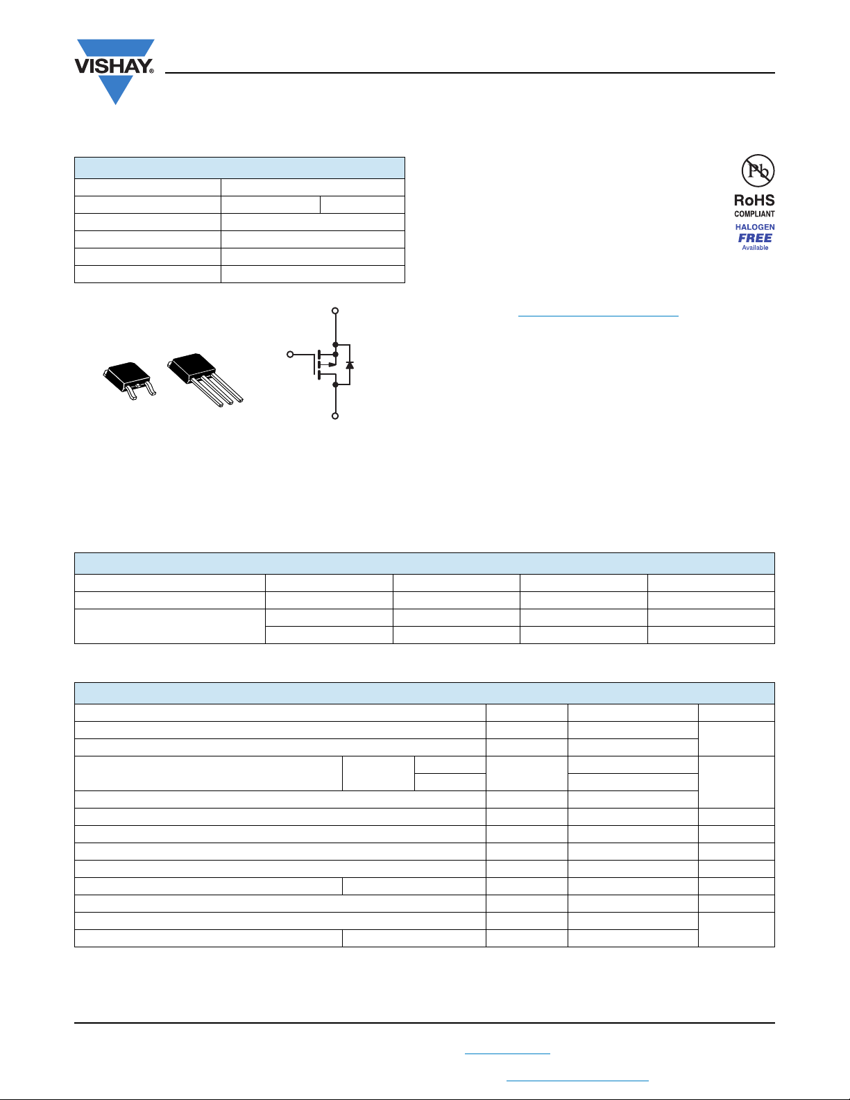
S
G
D
P-Channel MOSFET
IRFR9214, IRFU9214, SiHFR9214, SiHFU9214
Vishay Siliconix
Power MOSFET
PRODUCT SUMMARY
VDS (V) - 250
R
()V
DS(on)
Q
(Max.) (nC) 14
g
Q
(nC) 3.1
gs
Q
(nC) 6.8
gd
Configuration Single
DPAK
(TO-252)
D
G
IPAK
(TO-251)
D
S
= - 10 V 3.0
GS
S
D
G
FEATURES
•P-Channel
• Surface Mount (IRFR9214, SiHFR9214)
• Straight Lead (IRFU9214, SiHFU9214)
• Advanced Process Technology
• Fast Switching
• Fully Avalanche Rated
• Material categorization: For definitions of compliance
please see www.vishay.com/doc?99912
DESCRIPTION
Third generation power MOSFETs from Vishay utilize
advanced processing techniques to achieve low
on-resistance per silicon area. This benefit, combined with
the fast switching speed and ruggedized device design that
power MOSFETs are well known for, provides the designer
with an extremely efficient and reliable device for use in a
wide variety of applications.
The DPAK is designed for surface mounting using vapor
phase, infrared, or wave soldering techniques. The straight
lead version (IRFU, SiHFU series) is for through-hole
mounting applications. Power dissipation levels up to 1.5 W
are possible in typical surface mount applications.
ORDERING INFORMATION
Package DPAK (TO-252) DPAK (TO-252) DPAK (TO-252) IPAK (TO-251)
Lead (Pb)-free and Halogen-free SiHFR9214-GE3 SiHFR9214TRL-GE3 SiHFR9214TR-GE3 SiHFU9214-GE3
Lead (Pb)-free
IRFR9214PbF IRFR9214TRLPbF
SiHFR9214-E3 SiHFR9214TL-E3
a
a
IRFR9214TRPbF
SiHFR9214T-E3
a
a
IRFU9214PbF
SiHFU9214-E3
Note
a. See device orientation.
ABSOLUTE MAXIMUM RATINGS (TC = 25 °C, unless otherwise noted)
PARAMETER SYMBOL LIMIT UNIT
Drain-Source Voltage V
Gate-Source Voltage V
T
= 25 °C
Continuous Drain Current V
Pulsed Drain Current
a
at - 10 V
GS
C
= 100 °C - 1.7
C
DS
± 20
GS
I
D
IDM - 11
Linear Derating Factor 0.40 W/°C
Single Pulse Avalanche Energy
Repetitive Avalanche Current
Repetitive Avalanche Energy
Maximum Power Dissipation T
Peak Diode Recovery dV/dt
Operating Junction and Storage Temperature Range T
Soldering Recommendations (Peak Temperature)
b
a
a
= 25 °C P
c
d
C
for 10 s 260
E
AS
I
AR
E
AR
D
dV/dt - 5.0 V/ns
, T
J
stg
Notes
a. Repetitive rating; pulse width limited by maximum junction temperature (see fig. 11).
b. Starting T
c. I
SD
d. 1.6 mm from case.
S13-0166-Rev. D, 04-Feb-13
= 25 °C, L = 27 mH, Rg = 25 , IAS = - 2.7 A (see fig. 12).
J
- 2.7 A, dI/dt 600 A/μs, VDD VDS, TJ 150 °C.
1
For technical questions, contact: hvm@vishay.com
THIS DOCUMENT IS SUBJECT TO CHANGE WITHOUT NOTICE. THE PRODUCTS DESCRIBED HEREIN AND THIS DOCUMENT
ARE SUBJECT TO SPECIFIC DISCLAIMERS, SET FORTH AT www.vishay.com/doc?91000
- 250
- 2.7
100 mJ
- 2.7 A
5.0 mJ
50 W
- 55 to + 150
Document Number: 91282
V
AT
°C
IRFR9214, IRFU9214, SiHFR9214, SiHFU9214
D
S
G
S
D
G
www.vishay.com
THERMAL RESISTANCE RATINGS
PARAMETER SYMBOL MIN. TYP. MAX. UNIT
Maximum Junction-to-Ambient R
Maximum Junction-to-Ambient
(PCB Mount)
a
Maximum Junction-to-Case (Drain) R
thJA
R
thJA
thJC
- - 110
--50
--2.5
Note
a. When mounted on 1" square PCB (FR-4 or G-10 material).
SPECIFICATIONS (TJ = 25 °C, unless otherwise noted)
PARAMETER SYMBOL TEST CONDITIONS MIN. TYP. MAX. UNIT
Static
Drain-Source Breakdown Voltage V
V
Temperature Coefficient VDS/TJ Reference to 25 °C, ID = - 1 mA - - 0.25 - V/°C
DS
Gate-Source Threshold Voltage V
Gate-Source Leakage I
Zero Gate Voltage Drain Current I
Drain-Source On-State Resistance R
Forward Transconductance g
DS
GS(th)
V
GSS
DSS
VGS = - 10 V ID = - 1.7 A
DS(on)
fs
Dynamic
Input Capacitance C
Reverse Transfer Capacitance C
Total Gate Charge Q
Gate-Drain Charge Q
Turn-On Delay Time t
Rise Time t
Turn-Off Delay Time t
Fall Time t
Internal Drain Inductance L
iss
-75-
oss
-11-
rss
g
--3.1
gs
--6.8
gd
d(on)
r
d(off)
-17-
f
D
V
-20-
Between lead,
6 mm (0.25") from
package and center of
Internal Source Inductance L
S
die contact
Drain-Source Body Diode Characteristics
Continuous Source-Drain Diode Current I
Pulsed Diode Forward Current
a
Body Diode Voltage V
Body Diode Reverse Recovery Time t
Body Diode Reverse Recovery Charge Q
Forward Turn-On Time t
S
I
SM
SD
rr
rr
on
MOSFET symbol
showing the
integral reverse
p - n junction diode
TJ = 25 °C, IF = - 1.7 A, dI/dt = 100 A/μs
Notes
a. Repetitive rating; pulse width limited by maximum junction temperature (see fig. 11).
b. Pulse width 300 μs; duty cycle 2 %.
VGS = 0 V, ID = - 250 μA - 250 - - V
VDS = VGS, ID = - 250 μA - 2.0 - - 4.0 V
= ± 20 V - - ± 100 nA
GS
VDS = - 250 V, VGS = 0 V - - - 100
= - 200 V, VGS = 0 V, TJ = 125 °C - - - 500
V
DS
b
VDS = - 50 V, ID = - 1.7 A 0.9 - - S
VGS = 0 V,
V
= - 25 V,
DS
f = 1.0 MHz, see fig. 5
= - 1.7 A, VDS = - 200 V,
I
= - 10 V
GS
V
R
= 21 , RD = 70 , see fig. 10
g
TJ = 25 °C, IS = - 2.7 A, VGS = 0 V
D
see fig. 6 and 13
= - 125 V, ID = - 1.7 A,
DD
b
b
b
b
Intrinsic turn-on time is negligible (turn-on is dominated by LS and LD)
Vishay Siliconix
°C/W
--3.0
- 220 -
--14
-11-
-14-
-4.5-
-7.5-
--- 2.7
--- 11
--- 5.8V
- 150 220 ns
- 870 1300 nC
μA
pFOutput Capacitance C
nC Gate-Source Charge Q
ns
nH
A
THIS DOCUMENT IS SUBJECT TO CHANGE WITHOUT NOTICE. THE PRODUCTS DESCRIBED HEREIN AND THIS DOCUMENT
ARE SUBJECT TO SPECIFIC DISCLAIMERS, SET FORTH AT www.vishay.com/doc?91000
For technical questions, contact: hvm@vishay.com
S13-0166-Rev. D, 04-Feb-13
2
Document Number: 91282
IRFR9214, IRFU9214, SiHFR9214, SiHFU9214
www.vishay.com
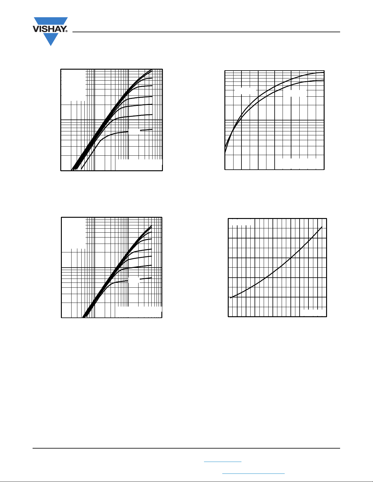
TYPICAL CHARACTERISTICS (25 °C, unless otherwise noted)
Vishay Siliconix
10
1
TOP
BOTTOM
VGS
-15V
-10V
-8.0V
-7.0V
-6.0V
-5.5V
-5.0V
-4.5V
-4.5V
D
-I , Drain-to-Source Current (A)
20μs PULSE W IDTH
°
T = 25 C
0.1
0.1 1 10 100
-V , Drain-to-Source Voltage (V)
DS
J
Fig. 1 - Typical Output Characteristics, TC = 25 °C
10
TOP
BOTTOM
VGS
-15V
-10V
-8.0V
-7.0V
-6.0V
-5.5V
-5.0V
-4.5V
10
°
T = 25 C
J
1
D
-I , Drain-to-Source Current (A)
0.1
4 5 6 7 8 9 10
-V , Gate-to-Source Voltage (V)
GS
T = 150 C
J
V = -50V
DS
20μs PULSE WIDTH
Fig. 3 - Typical Transfer Characteristics
2.5
2.0
I =
D
-2.7A
°
1
-4.5V
D
-I , Drain-to-Source Current (A)
20μs PULSE WIDTH
°
T = 150 C
0.1
0.1 1 10 100
-V , Drain-to-Source Voltage (V)
DS
J
Fig. 2 - Typical Output Characteristics, T
= 150 °C
C
1.5
1.0
(Normalized)
0.5
DS(on)
R , Drain-to-Source On Resistance
0.0
-60 -40 -20 0 20 40 60 80 100 120 140 160
T , Junction Temperature ( C)
J
V =
GS
°
-10V
Fig. 4 - Normalized On-Resistance vs. Temperature
S13-0166-Rev. D, 04-Feb-13
3
Document Number: 91282
For technical questions, contact: hvm@vishay.com
THIS DOCUMENT IS SUBJECT TO CHANGE WITHOUT NOTICE. THE PRODUCTS DESCRIBED HEREIN AND THIS DOCUMENT
ARE SUBJECT TO SPECIFIC DISCLAIMERS, SET FORTH AT www.vishay.com/doc?91000
www.vishay.com
0.1
1
10
100
10 100 1000
OPERAT ION IN THIS AREA LIMITED
BY R
DS(on)
Single Pulse
T T= 150 C
= 25 C
°
°
J
C
-V , Drain-to-Source Voltage (V)
-I , Drain Current (A)I , Drain Current (A)
DS
D
100us
1ms
10ms
IRFR9214, IRFU9214, SiHFR9214, SiHFU9214
Vishay Siliconix
400
300
200
C, Capacitance (pF)
100
0
1 10 100
V
=
0V,
GS
C
=
iss gs gd , ds
C
=
rss gd
C
=
oss ds gd
-V , Drain-to-Source Voltage (V)
DS
f = 1MHz
C
+ C
C SHORTED
C
C
+ C
C
iss
C
oss
C
rss
Fig. 5 - Typical Capacitance vs. Drain-to-Source Voltage
20
I =
-1.7 A
D
16
V =-200V
DS
V =-125V
DS
V =-50V
DS
10
°
T = 150 C
J
1
°
T = 25 C
J
SD
I , Reverse Drain Current (A)
V = 0 V
0.1
1.0 2.0 3.0 4.0 5.0
V ,Source-to-Drain Voltage (V)
SD
GS
Fig. 7 - Typical Source-Drain Diode Forward Voltage
12
8
4
GS
-V , Gate-to-Source Voltage (V)
0
0 3 6 9 12 15
Q , Total Gate Charge (nC)
G
Fig. 6 - Typical Gate Charge vs. Gate-to-Source Voltage
S13-0166-Rev. D, 04-Feb-13
THIS DOCUMENT IS SUBJECT TO CHANGE WITHOUT NOTICE. THE PRODUCTS DESCRIBED HEREIN AND THIS DOCUMENT
ARE SUBJECT TO SPECIFIC DISCLAIMERS, SET FORTH AT www.vishay.com/doc?91000
FOR TEST CIRCUIT
SEE FIGURE
13
4
For technical questions, contact: hvm@vishay.com
Fig. 8 - Maximum Safe Operating Area
Document Number: 91282
 Loading...