

Page 1
i179052
1
2
3
4
8
7
6
5
E
C
C
E
A
C
C
A
A
C
C
A
A
C
C
A
E
C
C
E
E
C
C
E
16
15
14
13
12
11
10
9
1
2
3
4
5
6
7
8
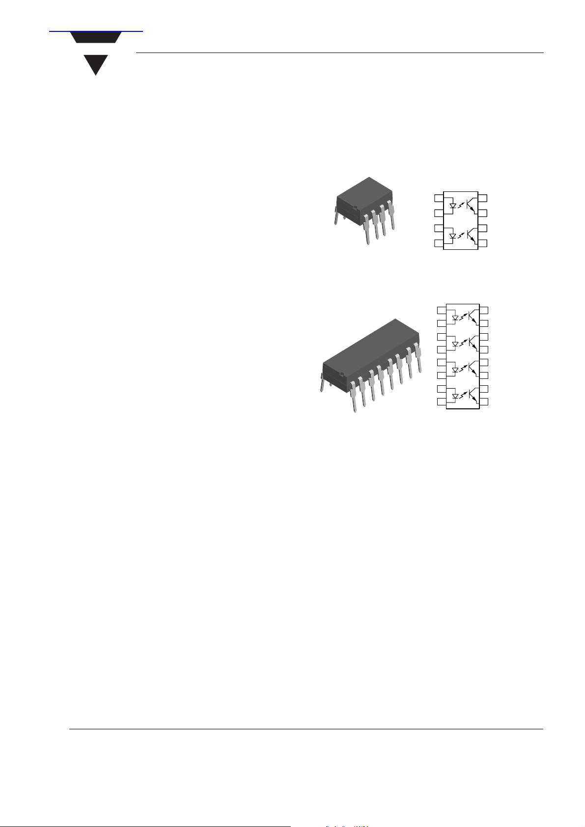
Dual Channel
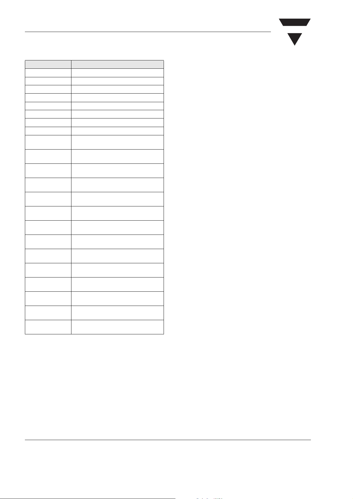
Quad Channel
查询ILD615供应商
VISHAY
ILD615/ ILQ615
Vishay Semiconductors
Optocoupler, Phototransistor Output (Dual, Quad Channel)
Features
• Identical Channel to Channel Footprint
• Dual and Quad Packages Feature:
- Reduced Board Space
- Lower Pin and Parts Count
- Better Channel to Channel CTR Match
- Improved Common Mode Rejection
• Isolation Test Voltage from Double Molded Package, 5300 V
• Lead-free component
• Component in accordance to RoHS 2002/95/EC
and WEEE 2002/96/EC
Agency Approvals
• UL1577, File No. E52744 System Code H or J,
Double Protection
• CSA 93751
• BSI IEC60950 IEC60965
• DIN EN 60747-5-2 (VDE0884)
DIN EN 60747-5-5 pending
Available with Option 1
RMS
Description
The ILD615/ ILQ615 are multi-channel phototransistor optocouplers that use GaAs IRLED emitters and
high gain NPN phototransistors. These devices are
constructed using over/under leadframe optical coupling and double molded insulation technology resulting a withstand test voltage of 7500 VAC
working voltage of 1700 V
The binned min./max. and linear CTR characteristics
make these devices well suited for DC or AC voltage
detection. Eliminating the phototransistor base connection provides added electrical noise immunity from
the transients found in many industrial control envi-
RMS
.
ronments.
Because of guaranteed maximum non-saturated and
saturated switching characteristics, the ILD615/
ILQ615 can be used in medium speed data I/O and
control systems. The binned min./max. CTR specification allow easy worst case interface calculations for
Document Number 83652
Rev. 1.3, 19-Apr-04
PEAK
and a
both level detection and switching applications. Interfacing with a CMOS logic is enhanced by the guaranteed CTR at I
= 1.0 mA.
F
www.vishay.com
1
Page 2
ILD615/ ILQ615
Vishay Semiconductors
Order Information
Part Remarks
ILD615-1 CTR 40 - 80 %, Dual Channel, DIP-8
ILD615-2 CTR 63 - 125 %, Dual Channel, DIP-8
ILD615-3 CTR 100 - 200 %, Dual Channel, DIP-8
ILD615-4 CTR 160 - 320 %, Dual Channel, DIP-8
ILQ615-1 CTR 40 - 80 %, Quad Channel, DIP-16
ILQ615-2 CTR 63 - 125 %, Quad Channel, DIP-16
ILQ615-3 CTR 100 - 200 %, Quad Channel, DIP-16
ILQ615-4 CTR 160 - 320 %, Quad Channel, DIP-16
ILD615-1X007 CTR 40 - 80 %, Dual Channel, SMD-8
(option 7)
ILD615-2X006 CTR 63 - 125 %, Dual Channel, DIP-8 400
mil (option 6)
ILD615-2X009 CTR 63 - 125 %, Dual Channel, SMD-8
(option 9)
ILD615-3X006 CTR 100 - 200 %, Dual Channel, DIP-8
400 mil (option 6)
ILD615-3X007 CTR 100 - 200 %, Dual Channel, SMD-8
(option 7)
ILD615-3X009 CTR 100 - 200 %, Dual Channel, SMD-8
(option 9)
ILD615-4X006 CTR 160 - 320 %, Dual Channel, DIP-8
400 mil (option 6)
ILD615-4X009 CTR 160 - 320 %, Dual Channel, SMD-8
(option 9)
ILQ615-1X009 CTR 40 - 80 %, Quad Channel, SMD-16
(option 9)
ILQ615-2X007 CTR 63 - 125 %, Quad Channel, SMD-16
(option 7)
ILQ615-3X006 CTR 100 - 200 %, Quad Channel, DIP-16
400 mil (option 6)
ILQ615-3X009 CTR 100 - 200 %, Quad Channel, SMD-16
(option 9)
ILQ615-4X007 CTR 160 - 320 %, Quad Channel, SMD-16
(option 7)
ILQ615-4X009 CTR 160 - 320 %, Quad Channel, SMD-16
(option 9)
For additional information on the available options refer to
Option Information.
VISHAY
www.vishay.com
2
Document Number 83652
Rev. 1.3, 19-Apr-04
Page 3
VISHAY
ILD615/ ILQ615
Vishay Semiconductors
Absolute Maximum Ratings
T
= 25 °C, unless otherwise specified
amb
Stresses in excess of the absolute Maximum Ratings can cause permanent damage to the device. Functional operation of the device is
not implied at these or any other conditions in excess of those given in the operational sections of this document. Exposure to absolute
Maximum Rating for extended periods of the time can adversely affect reliability.
Input
Parameter Test condition Symbol Val ue Unit
Reverse voltage V
Forward current I
Surge current I
Power dissipation P
Derate linearly from 25 °C 1.33 mW/°C
R
F
FSM
diss
6.0 V
60 mA
1.5 A
100 mW
Output
Parameter Test condition Symbol Val ue Unit
Collector-emitter breakdown
voltage
Emitter-collector breakdown
voltage
Collector current I
t < 1.0 ms I
Power dissipation P
Derate linearly from 25 °C 2.0 mW/°C
BV
BV
CEO
ECO
C
C
diss
70 V
7.0 V
50 mA
100 mA
150 mW
Coupler
Parameter Test condition Symbol Val ue Unit
Storage temperature T
Operating temperature T
Junction temperature T
Soldering temperature 2.0 mm distance from case
bottom
Package power dissipation,
ILD615
Derate linearly from 25 °C 5.33 mW/°C
Package power dissipation,
ILQ615
Derate linearly from 25 °C 6.67 mW/°C
Isolation test voltage t = 1.0 sec. V
Creepage ≥ 7.0 mm
Clearance ≥ 7.0 mm
Isolation resistance V
= 500 V, T
IO
V
= 500 V, T
IO
= 25 °C R
amb
= 100 °C R
amb
T
stg
amb
j
sld
ISO
IO
IO
- 55 to + 150 °C
- 55 to + 100 °C
100 °C
260 °C
400 mW
500 mW
5300 V
12
≥ 10
11
≥ 10
RMS
Ω
Ω
Document Number 83652
Rev. 1.3, 19-Apr-04
www.vishay.com
3
Page 4
ILD615/ ILQ615
VISHAY
Vishay Semiconductors
Electrical Characteristics
T
= 25 °C, unless otherwise specified
amb
Minimum and maximum values are testing requirements. Typical values are characteristics of the device and are the result of engineering
evaluation. Typical values are for information only and are not part of the testing requirements.
Input
Parameter Test condition Symbol Min Typ . Max Unit
Forward voltage I
Breakdown voltage I
Reverse current V
Capacitance V
Thermal resistance, junction to
lead
= 10 mA V
F
= 10 µAV
R
= 6.0 V I
R
= 0 V, f = 1.0 MHz C
R
R
F
BR
R
O
THJL
1.0 1.15 1.3 V
6.0 30 V
0.01 10 µA
25 pF
750 K/W
Output
Parameter Test condition Symbol Min Typ . Max Unit
Collector-emitter capacitance V
Collector-emitter leakage
current, -1, -2
Collector-emitter leakage
current, -3, -4
Collector-emitter breakdown
voltage
Emitter-collector breakdown
voltage
Thermal resistance, junction to
lead
Package transfer characteristics
Channel/Channel CTR match I
= 5.0 V, f = 1.0 MHz C
CE
= 10 V I
V
CE
= 10 V I
V
CE
I
= 0.5 mA BV
CE
I
= 0.1 mA BV
E
R
= 10 mA, VCE = 5.0 V CTRX/
F
CTRY
CE
CEO
CEO
CEO
ECO
THJL
6.8 pF
2.0 50 nA
5.0 100 nA
70 V
7.0 V
500 K/W
1 to 1 2 to 1
Coupler
Parameter Test condition Symbol Min Typ . Max Unit
Capacitance (input-output) V
Insulation resistance V
= 0 V, f = 1.0 MHz C
IO
= 500 V, TA = 25 °C R
IO
IO
S
10
12
0.8 pF
14
10
Channel to channel isolation 500 VAC
Current Transfer Ratio
Parameter Test condition Part Symbol Min Typ. Max Unit
Current Transfer Ratio
(collector-emitter saturated)
www.vishay.com
4
= 10 mA, VCE = 0.4 V ILD615-1
I
F
ILQ615-1
ILD615-2
ILQ615-2
ILD615-3
ILQ615-3
ILD615-4
ILQ615-4
CTR
CTR
CTR
CTR
CEsat
CEsat
CEsat
CEsat
25 %
40 %
60 %
100 %
Document Number 83652
Rev. 1.3, 19-Apr-04
Ω
Page 5

VISHAY
ILD615/ ILQ615
Vishay Semiconductors
Parameter Test condition Part Symbol Min Typ. Max Unit
Current Transfer Ratio
(collector-emitter)
IF = 10 mA, VCE = 5.0 V ILD615-1
ILQ615-1
= 1.0 mA, VCE = 5.0 V ILD615-2
I
F
CTR
CTR
CE
CE
40 60 80 %
13 30 %
ILQ615-2
I
= 10 mA, VCE = 5.0 V ILD615-3
F
I
= 1.0 mA, VCE = 5.0 V ILD615-4
F
ILQ615-3
CTR
CTR
CE
CE
63 80 125 %
22 45 %
ILQ615-4
= 10 mA, VCE = 5.0 V ILD615-1
I
F
CTR
CE
100 150 200 %
ILQ615-1
I
= 1.0 mA, VCE = 5.0 V ILD615-2
F
I
= 10 mA, VCE = 5.0 V ILD615-3
F
ILQ615-2
CTR
CTR
CE
CE
34 70 %
160 200 320 %
ILQ615-3
= 1.0 mA, VCE = 5.0 V ILD615-4
I
F
CTR
CE
56 90 %
ILQ615-4
Switching Non-saturated
Parameter Current Turn-on time Rise time Turn-off time Fall time Propagation
Test condition VCC = 5.0 V, RL = 75 Ω, 50 % of V
Symbol I
F
t
on
t
r
t
off
PP
t
f
Unit mA µs µs µs µs µs µs
ILD615-1 10 3.0 2.0 2.3 2.0 1.1 2.5
H-L
t
PHL
Propagation
L-H
t
PLH
Switching Saturated
Parameter Current Turn-on time Rise time Turn-off time Fall time Propagation
Test condition VCC = 5.0 V, RL = 1.0 kΩ, VTH = 1.5 V
Symbol I
F
t
on
t
r
t
off
t
f
Unit mA µs µs µs µs µs µs
ILD615-1
20 3.0 2.0 18 11 1.6 8.6
ILQ615-1
ILD615-2
10 4.3 2.8 25 14 2.6 7.2
ILQ615-2
ILD615-3
10 4.3 2.8 25 14 2.6 7.2
ILQ615-3
ILD615-4
5.0 6.0 4.6 25 15 5.4 7.4
ILQ615-4
H-L
t
PHL
Common Mode Transient Immunity
Parameter Test condition Symbol Min Typ. Max Unit
Common mode rejection output
high
Common mode rejection output
low
Common mode coupling
capacitance
= 50 V
V
CM
I
= 0 mA
F
V
= 50 V
CM
= 10 mA
I
F
, RL = 1.0 kΩ,
P-P
, RL = 1.0 kΩ,
P-P
CM
CM
C
CM
H
L
5000 V/µs
5000 V/µs
0.01 pF
Propagation
L-H
t
PLH
Document Number 83652
Rev. 1.3, 19-Apr-04
www.vishay.com
5
Page 6

ILD615/ ILQ615
iild615_04
I
F
t
R
V
O
t
D
t
S
t
F
t
PHL
t
PLH
VTH= 1.5 V
-60 -40 -20 0 20 40 60 80 100
120
100
80
60
40
0
20
Ta - Ambient Temperature - °C
IF - Maximum LED Current - mA
TJ (MAX) = 100 °C
iild615_05
iild615_06
-60 -40 -20 0 20 40 60 80 100
200
100
0
50
Ta - Ambient Temperature - °C
P
LED
- LED Power - mW
150
Vishay Semiconductors
Typical Characteristics (Tamb = 25 °C unless otherwise specified)
VCC=5V
VISHAY
iild615_01
iild615_02
IF=10mA
V
O
F = 10 KHz,
RL = 75 Ω
DF = 50%
Figure 1. Non-saturated Switching Timing
F=10KHz,
DF=50%
VCC=5V
R
L
V
O
Figure 4. Saturated Switching Timing
Figure 2. Saturated Switching Timing
I
F
t
V
iild615_03
www.vishay.com
6
PLH
O
t
t
D
R
t
on
Figure 3. Non-saturated Switching Timing
t
PLH
t
S
Figure 5. Maximum LED Current vs. Ambient Temperature
50%
t
F
t
off
Figure 6. Maximum LED Power Dissipation
Document Number 83652
Rev. 1.3, 19-Apr-04
Page 7

VISHAY
iild615_10
.1 10 100
1000
100
10
1
.1
VCE- Collector-Emitter Voltage - V
I
CE
- Collector Current - mA
Rth = 500 °C/W
25 °C
50 °C
75 °C
90 °C
1
iild615_11
CTRNF - Normalized CTR Factor
.1 1 10 100
2.0
1.5
1.0
0.5
0.0
IF- LED Current - mA
NCTRce
TA=25°C
Normalized to:
V
CE
=10V,IF= 5 mA,
CTRce(sat) VCE= 0.4 V
NCTRce(sat)
iild615_12
CTRNF - Normalized CTR Factor
.1 1 10 100
2.0
1.5
1.0
0.5
0.0
IF- LED Current - mA
NCTRce
TA=50°C
Normalized to:
V
CE
=10V,IF= 5 mA,
CTRce(sat) VCE= 0.4 V
NCTRce(sat)
1.4
3
1.
1.2
1.1
1.0
0.9
0.8
VF - Forward Voltage - V
0.7
iild615_07
ILD615/ ILQ615
Vishay Semiconductors
Ta = –55 °C
Ta=25°C
Ta = 85° C
100101.1
IF - Forward Current - mA
Figure 7. Forward Voltage vs. Forward Current
If(pk) - Peak LED Current - mA
iild615_08
10000
Duty F actor
.005
.01
1000
.02
.05
.1
.2
.5
100
10
10-610-510-410-310-210-110010
t - LED Pulse Duration - s
τ
ˇ
t
DF=/t
Figure 8. Peak LED Current vs. Pulse Duration, Tau
200
150
Figure 10. Maximum Collector Current vs. Collector Voltage
τ
1
Figure 11. Normalization Factor for Non-saturated and Saturated
CTR vs. I
F
100
- Detector Power - mW
50
DET
P
0
-60 -40 -20 0 20 40 60 80 100
iild615_09
Ta - Ambient Temperature - °C
Figure 9. Maximum Detector Power Dissipation
Document Number 83652
Rev. 1.3, 19-Apr-04
Figure 12. Normalization Factor for Non-saturated and Saturated
CTR vs. I
F
www.vishay.com
7
Page 8

ILD615/ ILQ615
iild615_16
100806040200-20
10
10
10
10
10
10
10
10
-2
-1
0
1
2
3
4
5
TA- Ambient Temperature - °C
I
CEO
- Collector-Emitter - nA
Vce=10V
Typical
iild615_17
RL-LoadResistor-kΩ
100101.1
1
10
100
1000
1.0
1.5
2.0
4.0
tpLH
tpHL
t
pLH
- Propagation Low-High µs
t
pHL
- Propagation High-Low µs
IF=10mA
V
CC
= 5 V, Vth = 1.5 V
2.5
3.0
3.5
iild615_18
RL- Collector Load Resistor - kΩ
100101.1
1
10
100
1000
1.0
1.5
2.0
2.5
tpLH
tpHL
t
pLH
- Propagation Low-High µs
t
pHL
- Propagation High-Low µs
IF=10mA
V
CC
=5V,Vth=1.5V
Vishay Semiconductors
2.0
Normalized to:
V
=10V,IF= 5 mA,
CE
1.5
CTRce(sat) VCE= 0.4 V
VISHAY
1.0
0.5
NCTRce
NCTRce(sat)
TA=70°C
0.0
CTRNF - Normalized CTR Factor
.1 1 10 100
IF- LED Current - mA
iild615_13
Figure 13. Normalization Factor for Non-saturated and Saturated
CTR vs. I
2.0
Normalized to:
V
=10V,IF= 5 mA,
CE
1.5
CTRce(sat) VCE= 0.4 V
1.0
NCTRce
0.5
0.0
CTRNF - Normalized CTR Factor
.1 1 10 100
F
NCTRce(sat)
TA= 100 °C
IF- LED Current - mA
Figure 16. Collector Emitter Leakage vs. Temperature
iild615_14
Figure 14. Normalization Factor for Non-saturated and Saturated
CTR vs. I
F
35
30
25
50°C
20
15
10
- Collector Current - mA
5
CE
I
25°C
85°C
70°C
0
iild615_15
40
IF- LED Current - mA
60503020100
Figure 15. Collector-Emitter Current vs. Temperature and LED
www.vishay.com
8
Current
Figure 17. -1, Propagation Delay vs. Collector Load Resistor
Figure 18. -2, -3, Propagation Delay vs. Collector Load Resistor
Document Number 83652
Rev. 1.3, 19-Apr-04
Page 9

VISHAY
1000
IF=10mA
V
CC
100
ILD615/ ILQ615
Vishay Semiconductors
Figure 19. -4, Propagation Delay vs. Collector Load Resistor
2.5
= 5 V, Vth = 1.5 V
2.0
tpLH
- Propagation Low-High µs
pLH
t
iild615_19
10
tpHL
1
RL- Collector Load Resistor - kΩ
1.5
1.0
100101.1
Package Dimensions in Inches (mm)
pin one ID
i178006
.255 (6.48)
.268 (6.81)
.030 (0.76)
.045 (1.14)
4° typ.
.050 (1.27)
.018 (.46)
.022 (.56)
4
3
5
6
.379 (9.63)
.390 (9.91)
1
2
78
.031 (0.79)
.130 (3.30)
.150 (3.81)
.020 (.51 )
.035 (.89 )
.100 (2.54) typ.
- Propagation High-Low µs
t
pHL
ISO Method A
.300 (7.62)
typ.
10°
3°–9°
.008 (.20)
.012 (.30)
.110 (2.79)
.130 (3.30)
.230(5.84)
.250(6.35)
Document Number 83652
Rev. 1.3, 19-Apr-04
www.vishay.com
9
Page 10

ILD615/ ILQ615
Vishay Semiconductors
Package Dimensions in Inches (mm)
87654321
910111213141516
.779 (19.77 )
.790 (20.07)
VISHAY
pin one ID
.255 (6.48)
.265 (6.81)
ISO Method A
4°
.018 (.46)
.022 (.56)
i178007
Option 6
.407 (10.36)
.391 (9.96)
.307 (7.8)
.291 (7.4)
.014 (0.35)
.010 (0.25)
.400 (10.16)
.430 (10.92)
.030 (.76)
.045 (1.14)
.100 (2.54)typ.
.028 (0.7)
MIN.
.031(.79)
Option 7
.300 (7.62)
TYP.
.315 (8.0)
MIN.
.331 (8.4)
MIN.
.406 (10.3)
MAX.
.130 (3.30)
.150 (3.81)
.020(.51)
.035 (.89)
.050 (1.27)
.180 (4.6)
.160 (4.1)
.300 (7.62)
3°–9°
.0040 (.102)
.0098 (.249)
typ.
10°
typ.
.008 (.20)
.012 (.30)
.110 (2.79)
.130 (3.30)
Option 9
.375 (9.53)
.395 (10.03)
.300 (7.62)
ref.
.020 (.51)
.040 (1.02)
.315 (8.00)
min.
.230 (5.84)
.250 (6.35)
.012 (.30) typ.
15° max.
18450
www.vishay.com
10
Document Number 83652
Rev. 1.3, 19-Apr-04
Page 11

VISHAY
ILD615/ ILQ615
Vishay Semiconductors
Ozone Depleting Substances Policy Statement
It is the policy of Vishay Semiconductor GmbH to
1. Meet all present and future national and international statutory requirements.
2. Regularly and continuously improve the performance of our products, processes, distribution and
operatingsystems with respect to their impact on the health and safety of our employees and the public, as
well as their impact on the environment.
It is particular concern to control or eliminate releases of those substances into the atmosphere which are
known as ozone depleting substances (ODSs).
The Montreal Protocol (1987) and its London Amendments (1990) intend to severely restrict the use of ODSs
and forbid their use within the next ten years. Various national and international initiatives are pressing for an
earlier ban on these substances.
Vishay Semiconductor GmbH has been able to use its policy of continuous improvements to eliminate the use
of ODSs listed in the following documents.
1. Annex A, B and list of transitional substances of the Montreal Protocol and the London Amendments
respectively
2. Class I and II ozone depleting substances in the Clean Air Act Amendments of 1990 by the Environmental
Protection Agency (EPA) in the USA
3. Council Decision 88/540/EEC and 91/690/EEC Annex A, B and C (transitional substances) respectively.
Vishay Semiconductor GmbH can certify that our semiconductors are not manufactured with ozone depleting
substances and do not contain such substances.
We reserve the right to make changes to improve technical design
and may do so without further notice.
Parameters can vary in different applications. All operating parameters must be validated for each
customer application by the customer. Should the buyer use Vishay Semiconductors products for any
unintended or unauthorized application, the buyer shall indemnify Vishay Semiconductors against all
claims, costs, damages, and expenses, arising out of, directly or indirectly, any claim of personal
damage, injury or death associated with such unintended or unauthorized use.
Vishay Semiconductor GmbH, P.O.B. 3535, D-74025 Heilbronn, Germany
Telephone: 49 (0)7131 67 2831, Fax number: 49 (0)7131 67 2423
Document Number 83652
Rev. 1.3, 19-Apr-04
www.vishay.com
11
 Loading...