

Small Signal Zener Diodes
Features
• Silicon Planar Power Zener Diodes
• The Zener voltages are graded according
to the international E 24 standard
• Standard Zener voltage tolerance is ± 5 %;
Replace "C" with "B" for ± 2 % tolerance
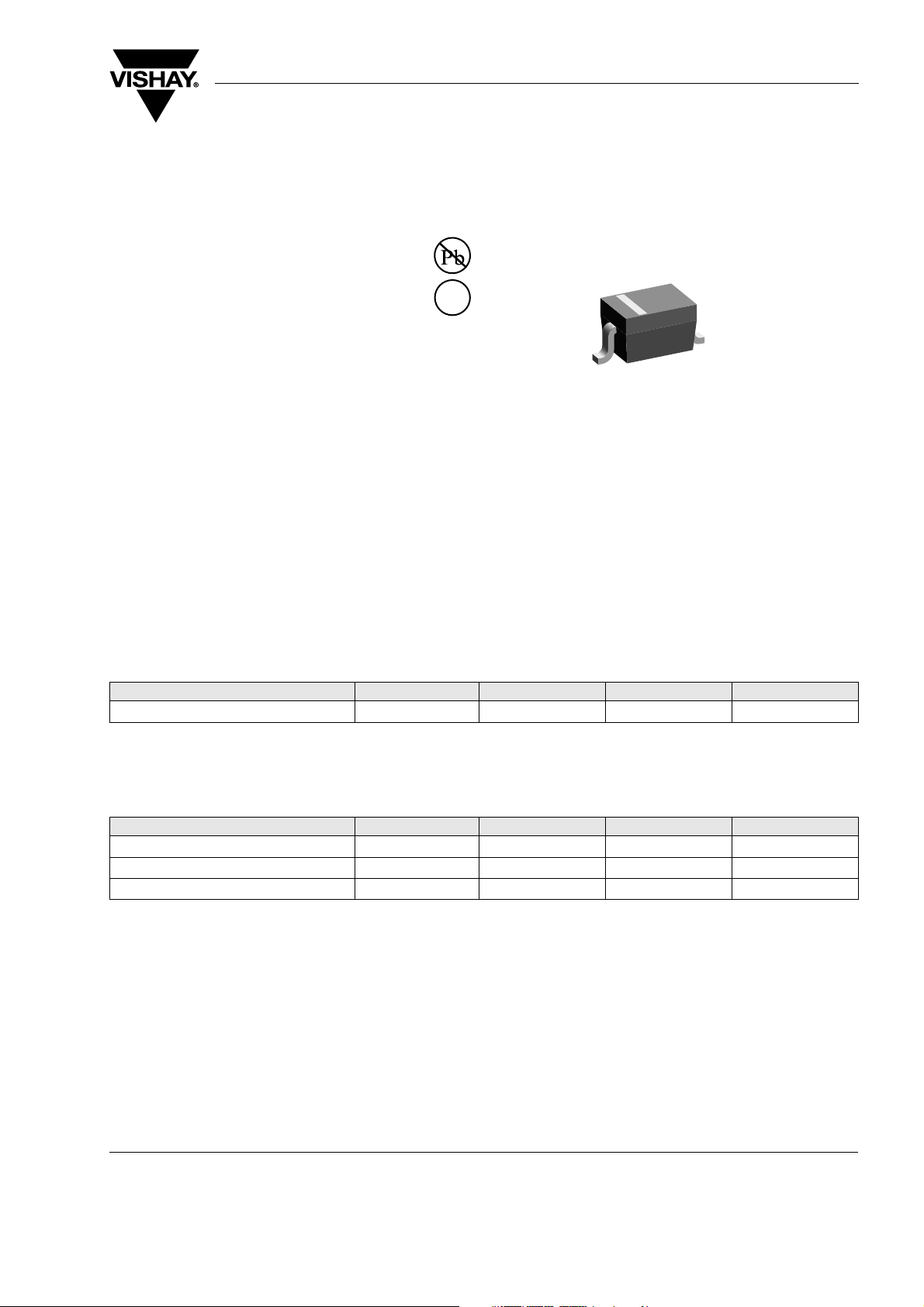
• Lead (Pb)-free component
• Component in accordance to RoHS 2002/95/EC
and WEEE 2002/96/EC
Mechanical Data
Case: SOD323 Plastic case
Weight: approx. 5.0 mg
Packaging Codes/Options:
GS18/10 k per 13" reel (8 mm tape), 10 k/box
GS08/3 k per 7" reel (8 mm tape), 15 k/box
e3
BZX384-V-Series
Vishay Semiconductors
20145
Absolute Maximum Ratings
T
= 25 °C, unless otherwise specified
amb
Parameter Test condition Symbol Val ue Unit
Power dissipation
1)
Device on fiberglass substrate
Thermal Characteristics
T
= 25 °C, unless otherwise specified
amb
Parameter Test condition Symbol Val ue Unit
Thermal resistance junction to ambient air R
Junction temperature T
Storage temperature range T
1)
Valid that electrodes are kept at ambient temperature
P
tot
thJA
stg
1)
200
1)
650
j
150 °C
- 65 to + 150 °C
mW
K/W
Document Number 85764
Rev. 1.6, 17-May-06
www.vishay.com
1

BZX384-V-Series
Vishay Semiconductors
Electrical Characteristics
Partnumber Marking
Code
BZX384C2V4-V W1 2.2 2.6 70 (≤ 100) 275 5 - 9 - 4 1 50 1
BZX384C2V7-V W2 2.5 2.9 75 (≤ 100) 300 (≤ 600) 5 - 9 - 4 1 20 1
BZX384C3V0-V W3 2.8 3.2 80 (≤ 95) 325 (≤ 600) 5 - 9 - 3 1 10 1
BZX384C3V3-V W4 3.1 3.5 85 (≤ 95) 350 (≤ 600) 5 - 8 - 3 1 5 1
BZX384C3V6-V W5 3.4 3.8 85 (≤ 90) 375 (≤ 600) 5 - 8 - 3 1 5 1
BZX384C3V9-V W6 3.7 4.1 85 (≤ 90) 400 (≤ 600) 5 - 7 - 3 1 3 1
BZX384C4V3-V W7 4 4.6 80 (≤ 90) 410 (≤ 600) 5 - 6 - 1 1 3 1
BZX384C4V7-V W8 4.4 5 50 (≤ 80) 425 (≤ 500) 5 - 5 2 1 3 2
BZX384C5V1-V W9 4.8 5.4 40 (≤ 60) 400 (≤ 480) 5 - 3 4 1 2 2
BZX384C5V6-V WA 5.2 6 15 (≤ 40) 80 (≤ 400) 5 - 2 6 1 1 2
BZX384C6V2-V WB 5.8 6.6 6.0 (≤ 10) 40 (≤ 150) 5 - 1 7 1 3 4
BZX384C6V8-V WC 6.4 7.2 6.0 (≤ 15) 30 (≤ 80) 5 2 7 1 2 4
BZX384C7V5-V WD 7 7.9 6.0 (≤ 15) 30 (≤ 80) 5 3 7 1 1 5
BZX384C8V2-V WE 7.7 8.7 6.0 (≤ 15) 40 (≤ 80) 5 4 7 1 0.7 5
BZX384C9V1-V WF 8.5 9.6 6.0 (≤ 15) 40 (≤ 100) 5 5 8 1 0.5 6
BZX384C10-V WG 9.4 10.6 8.0 (≤ 20) 50 (≤ 150) 5 5 8 1 0.2 7
BZX384C11-V WH 10.4 11.6 10 (≤ 20) 50 (≤ 150) 5 5 9 1 0.1 8
BZX384C12-V WI 11.4 12.7 10 (≤ 25) 50 (≤ 150) 5 6 9 1 0.1 8
BZX384C13-V WK 12.4 14.1 10 (≤ 30) 50 (≤ 170) 5 7 9 1 0.1 8
BZX384C15-V WL 13.8 15.6 10 (≤ 30) 50 (≤ 200) 5 7 9 1 0.05 0.7 V
BZX384C16-V WM 15.3 17.1 10 (≤ 40) 50 (≤ 200) 5 8 9.5 1 0.05 0.7 V
BZX384C18-V WN 16.8 19.1 10 (≤ 45) 50 (≤ 225) 5 8 9.5 1 0.05 0.7 V
BZX384C20-V WO 18.8 21.2 15 (≤ 55) 60 (≤ 225) 5 8 10 1 0.05 0.7 V
BZX384C22-V WP 20.8 23.3 20 (≤ 55) 60 (≤ 250) 5 8 10 1 0.05 0.7 V
BZX384C24-V WR 22.8 25.6 25 (≤ 70) 60 (≤ 250) 5 8 10 1 0.05 0.7 V
BZX384C27-V WS 25.1 28.9 25 (≤ 80) 65 (≤ 300) 2 8 10 0.5 0.05 0.7 V
BZX384C30-V WT 28 32 30 (≤ 80) 70 (≤ 300) 2 8 10 0.5 0.05 0.7 V
BZX384C33-V WU 31 35 35 (≤ 80) 75 (≤ 325) 2 8 10 0.5 0.05 0.7 V
BZX384C36-V WW 34 38 35 (≤ 90) 80 (≤ 350) 2 8 10 0.5 0.05 0.7 V
BZX384C39-V WX 37 41 40 (≤ 130) 80 (≤ 350) 2 10 12 0.5 0.05 0.7 V
BZX384C43-V WY 40 46 45 (≤ 150) 85 (≤ 375) 2 10 12 0.5 0.05 0.7 V
BZX384C47-V WZ 44 50 50 (≤ 170) 85 (≤ 375) 2 10 12 0.5 0.05 0.7 V
BZX384C51-V X1 48 54 60 (≤ 180) 85 (≤ 400) 2 10 12 0.5 0.05 0.7 V
BZX384C56-V X2 52 60 70 (≤ 200) 100 (≤ 425) 2 9 11 0.5 0.05 0.7 V
BZX384C62-V X3 58 66 80 (≤ 215) 100 (≤ 450) 2 9 12 0.5 0.05 0.7 V
BZX384C68-V X4 64 72 90 (≤ 240) 150 (≤ 475) 2 10 12 0.5 0.05 0.7 V
BZX384C75-V X5 70 79 95 (≤ 255) 170 (≤ 500) 2 10 12 0.5 0.05 0.7 V
(1)
Measured with pulses tp = 5 ms
Zener Voltage
Range
Dynamic Resistance Te s t
Current
Temperature
Coefficient of
Zener Voltage
VZ at I
ZT1
V Ω Ω mA
rzj at I
ZT1
rzj at I
ZT2
I
ZT1
αVZ at I
10-4/°C
min max typ typ min max
ZT1
Te s t
Reverse Leakage
Current
at I
ZT2
mA µA V
Current
IR at V
R
Znom.
Znom.
Znom.
Znom.
Znom.
Znom.
Znom.
Znom.
Znom.
Znom.
Znom.
Znom.
Znom.
Znom.
Znom.
Znom.
Znom.
Znom.
www.vishay.com
2
Document Number 85764
Rev. 1.6, 17-May-06

BZX384-V-Series
Vishay Semiconductors
Electrical Characteristics
Partnumber Marking
Code
BZX384B2V4-V W1 2.35 2.45 70 (≤ 100) 275 5 - 9 - 4 1 50 1
BZX384B2V7-V W2 2.65 2.75 75 (≤ 100) 300 (≤ 600) 5 - 9 - 4 1 20 1
BZX384B3V0-V W3 2.94 3.06 80 (≤ 95) 325 (≤ 600) 5 - 9 - 3 1 10 1
BZX384B3V3-V W4 3.23 3.37 85 (≤ 95) 350 (≤ 600) 5 - 8 - 3 1 5 1
BZX384B3V6-V W5 3.53 3.67 85 (≤ 90) 375 (≤ 600) 5 - 8 - 3 1 5 1
BZX384B3V9-V W6 3.82 3.98 85 (≤ 90) 400 (≤ 600) 5 - 7 - 3 1 3 1
BZX384B4V3-V W7 4.21 4.39 80 (≤ 90) 410 (≤ 600) 5 - 6 - 1 1 3 1
BZX384B4V7-V W8 4.61 4.79 50 (≤ 80) 425 (≤ 500) 5 - 5 2 1 3 2
BZX384B5V1-V W9 5.00 5.20 40 (≤ 60) 400 (≤ 480) 5 - 3 4 1 2 2
BZX384B5V6-V WA 5.49 5.71 15 (≤ 40) 80 (≤ 400) 5 - 2 6 1 1 2
BZX384B6V2-V WB 6.08 6.32 6.0 (≤ 10) 40 (≤ 150) 5 - 1 7 1 3 4
BZX384B6V8-V WC 6.66 6.94 6.0 (≤ 15) 30 (≤ 80) 5 2 7 1 2 4
BZX384B7V5-V WD 7.35 7.65 6.0 (≤ 15) 30 (≤ 80) 5 3 7 1 1 5
BZX384B8V2-V WE 8.04 8.36 6.0 (≤ 15) 40 (≤ 80) 5 4 7 1 0.7 5
BZX384B9V1-V WF 8.92 9.28 6.0 (≤ 15) 40 (≤ 100) 5 5 8 1 0.5 6
BZX384B10-V WG 9.80 10.2 8.0 (≤ 20) 50 (≤ 150) 5 5 8 1 0.2 7
BZX384B11-V WH 10.8 11.2 10 (≤ 20) 50 (≤ 150) 5 5 9 1 0.1 8
BZX384B12-V WI 11.8 12.2 10 (≤ 25) 50 (≤ 150) 5 6 9 1 0.1 8
BZX384B13-V WK 12.7 13.3 10 (≤ 30) 50 (≤ 170) 5 7 9 1 0.1 8
BZX384B15-V WL 14.7 15.3 10 (≤ 30) 50 (≤ 200) 5 7 9 1 0.05 0.7 V
BZX384B16-V WM 15.7 16.3 10 (≤ 40) 50 (≤ 200) 5 8 9.5 1 0.05 0.7 V
BZX384B18-V WN 17.6 18.4 10 (≤ 45) 50 (≤ 225) 5 8 9.5 1 0.05 0.7 V
BZX384B20-V WO 19.6 20.4 15 (≤ 55) 60 (≤ 225) 5 8 10 1 0.05 0.7 V
BZX384B22-V WP 21.6 22.4 20 (≤ 55) 60 (≤ 250) 5 8 10 1 0.05 0.7 V
BZX384B24-V WR 23.5 24.5 25 (≤ 70) 60 (≤ 250) 5 8 10 1 0.05 0.7 V
BZX384B27-V WS 26.5 27.5 25 (≤ 80) 65 (≤ 300) 2 8 10 0.5 0.05 0.7 V
BZX384B30-V WT 29.4 30.6 30 (≤ 80) 70 (≤ 300) 2 8 10 0.5 0.05 0.7 V
BZX384B33-V WU 32.3 33.7 35 (≤ 80) 75 (≤ 325) 2 8 10 0.5 0.05 0.7 V
BZX384B36-V WW 35.3 36.7 35 (≤ 90) 80 (≤ 350) 2 8 10 0.5 0.05 0.7 V
BZX384B39-V WX 38.2 39.8 40 (≤ 130) 80 (≤ 350) 2 10 12 0.5 0.05 0.7 V
BZX384B43-V WY 42.1 43.9 45 (≤ 150) 85 (≤ 375) 2 10 12 0.5 0.05 0.7 V
BZX384B47-V WZ 46.1 47.9 50 (≤ 170) 85 (≤ 375) 2 10 12 0.5 0.05 0.7 V
BZX384B51-V X1 50.0 52.0 60 (≤ 180) 85 (≤ 400) 2 10 12 0.5 0.05 0.7 V
BZX384B56-V X2 54.9 57.1 70 (≤ 200) 100 (≤ 425) 2 9 11 0.5 0.05 0.7 V
BZX384B62-V X3 60.8 63.2 80 (≤ 215) 100 (≤ 450) 2 9 12 0.5 0.05 0.7 V
BZX384B68-V X4 66.6 69.4 90 (≤ 240) 150 (≤ 475) 2 10 12 0.5 0.05 0.7 V
BZX384B75-V X5 73.5 76.5 95 (≤ 255) 170 (≤ 500) 2 10 12 0.5 0.05 0.7 V
Zener Voltage
Range
Dynamic Resistance Te st
Current
Temperature
Coefficient of
Zener Voltage
VZ at I
ZT1
V Ω Ω mA
rzj at I
ZT1
rzj at I
ZT2
I
ZT1
αVZ at I
10-4/°C
min max typ typ min max
ZT1
Te st
Reverse Leakage
Current
atI
ZT2
mA µA V
Current
IR at V
R
Znom.
Znom.
Znom.
Znom.
Znom.
Znom.
Znom.
Znom.
Znom.
Znom.
Znom.
Znom.
Znom.
Znom.
Znom.
Znom.
Znom.
Znom.
Document Number 85764
Rev. 1.6, 17-May-06
www.vishay.com
3

BZX384-V-Series
Vishay Semiconductors
Typical Characteristics
T
= 25 °C, unless otherwise specified
amb
mA
3
10
2
10
I
10
F
1
-1
10
-2
10
-3
10
-4
10
-5
10
0 0.2 0.4 0.6 0.8 1 V
18114
TJ = 100 °C
T
= 25 °C
J
V
Figure 1. Forward characteristics
r
1000
zj
5
4
3
2
TJ = 25 °C
100
5
4
3
2
100
5
4
3
2
1
0.1 25 25110
F
18117
2.7
3.6
4.7
5.1
5.6
25100 mA
I
Z
Figure 4. Dynamic Resistance vs. Zener Current
mW
250
200
P
tot
150
100
50
0
0 100 200 °C
18192
T
amb
Figure 2. Admissible Power Dissipation vs. Ambient Temperature
°C/W
3
10
7
5
4
3
r
thA
0.5
2
2
0.2
10
7
0.1
5
0.05
4
3
0.02
2
0.01
10
18116
7
5
4
3
2
1
= 0
tp
tp
P
T
T
10-510-410-310-210-1110s
tp
I
Figure 3. Pulse Thermal Resistance vs. Pulse Duration
pF
1000
7
5
4
C
tot
3
VR = 2 V
2
VR = 1 V
Tj = 25 °C
100
7
5
4
3
2
VR = 2 V
VR = 1 V
10
18193
1
2345 2345
10 100 V
V
Z
Figure 5. Capacitance vs. Zener Voltage
Ω
100
5
4
3
r
zj
2
10
5
4
3
2
1
0.1
25 25
18119
110
= 25 °C
T
J
33
27
22
18
15
12
25
I
Z
10
6.8/8.2
6.2
Figure 6. Dynamic Resistance vs. Zener Current
100 mA
www.vishay.com
4
Document Number 85764
Rev. 1.6, 17-May-06

BZX384-V-Series
Vishay Semiconductors
Ω
3
10
7
5
4
r
3
47 + 51
zj
10
10
18120
43
39
2
36
2
7
5
4
3
2
0.1
2345 2345
1 10 mA
I
Tj = 25 °C
Z
Figure 7. Dynamic Resistance vs. Zener Current
Ω
3
10
5
r
= R
zth
4
3
2
r
zth
2
10
5
4
3
2
x VZ x
thA
ΔΔV
Z
T
j
10
5
4
3
2
negative
positive
1
18121
1
2345 2345
10 100 V
VZ at IZ = 5 mA
Figure 8. Thermal Differential Resistance vs. Zener Voltage
mV/°C
25
20
Δ
V
Z
Δ
T
j
15
5 mA
1 mA
=
I
Z
20 mA
10
5
0
- 5
18135
1
2345 2345
10 100 V
VZ at IZ = 5 mA
≥
V 27 V, I = 2 mA
Figure 10. Temperature Dependence of Zener Voltage vs. Zener
Voltage
V
0.8
0.7
VZ at IZ = 5 mA
0.6
0.5
V
Δ
Z
0.4
0.3
0.2
0.1
0
- 1
- 0.2
020406080
18124
25
15
3.6
100 120 140 C
T
j
10
8
7
6.2
5.9
5.6
5.1
4.7
Figure 11. Change of Zener Voltage vs. Junction Temperature
Ω
100
7
5
4
r
3
zj
2
10
7
5
4
3
2
1
1
18122
2345 2345
Figure 9. Dynamic Resistance vs. Zener Voltage
Document Number 85764
Rev. 1.6, 17-May-06
Tj = 25 °C
I
= 5 mA
Z
10 100 V
V
Z
V
9
8
7
Δ
V
6
Z
VZ at IZ = 2 mA
51
5
4
3
43
36
2
1
0
- 1
0
20 40 120
18194
80 140 °C
60
100
I
= 2 mA
Z
T
j
Figure 12. Change of Zener Voltage vs. Junction Temperature
www.vishay.com
5

BZX384-V-Series
Vishay Semiconductors
mV/°C
100
80
V
Δ
Z
Δ
T
j
IZ = 5 mA
60
40
20
0
18195
0
20 40 80
60 100 V
VZ at IZ = 2 mA
Figure 13. Temperature Dependence of Zener Voltage vs. Zener
Voltage
V
1.6
V
= r
x I
Δ
Z
zth
1.4
IZ = 5 mA
1.2
V
Δ
V
Z
Z
1
Z
≥
27 V; IZ = 2 mA
0.8
0.6
0.4
0.2
0
- 0.2
- 0.4
18196
1
2345 2345
10 100 V
VZ at IZ = 5 mA
Figure 14. Change of Zener voltage from turn-on up to the point of
thermal equilibrium vs. Zener voltage
mA
50
Tj = 25 °C
40
l
z
2.7
3.3
3.9
4.7
5.6
6.8
30
20
Test Current I
10
0
0 10 V
18111
Z
5 mA
1
2345678 9
V
Z
Figure 16. Breakdown Characteristics
mA
30
l
z
20
10
Test Current I
5 mA
0
0 40 V
18112
10
12
15
18
22
Z
10 20 30
V
Z
27
Figure 17. Breakdown Characteristics
8.2
Tj = 25 °C
33
36
V
5
= r
x I
V
Δ
Z
zth
Z
4
Δ
V
Z
3
IZ = 5 mA
2
18160
1
0
0
20 40 60 80
I
= 2.5 mA
Z
VZ at IZ = 5 mA
100 V
Figure 15. Change of Zener voltage from turn-on up to the point of
thermal equilibrium vs. Zener voltage
www.vishay.com
6
mA
10
8
l
z
39
43
51
47
6
4
Test Current I
2 mA
Z
2
0
10
0 100 V
18191
20 30 40 50 60 70 8090
V
Z
Figure 18. Breakdown Characteristics
Document Number 85764
Rev. 1.6, 17-May-06
Tj = 25 °C
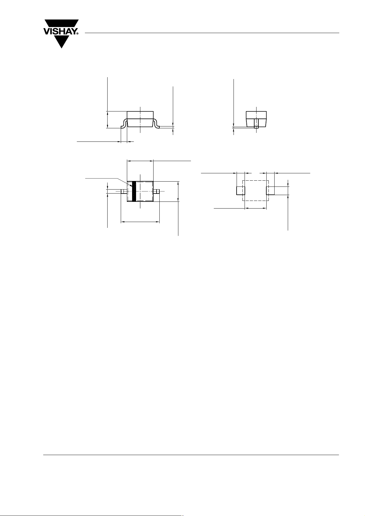
Package Dimensions in mm (Inches): SOD323
0.8 (0.031)
1.15 (0.045)
0.10 (0.004)
0.15 (0.006)
0.25 (0.010) min
BZX384-V-Series
Vishay Semiconductors
0.1 (0.004) max
cathode bar
2.85 (0.112)
0.20 (0.008)
0.40 (0.016)
Document no.: S8-V-3910.02-001 (4)
Rev. 03 - Date: 08.November 2004
17443
2.50 (0.098)
1.95 (0.077)
1.60 (0.063)
1.1 (0.043)
1.5 (0.059)
foot print recommendation:
0.6 (0.024)
1.6 (0.063)
0.6 (0.024)
0.6 (0.024)
Document Number 85764
Rev. 1.6, 17-May-06
www.vishay.com
7

BZX384-V-Series
Vishay Semiconductors
Ozone Depleting Substances Policy Statement
It is the policy of Vishay Semiconductor GmbH to
1. Meet all present and future national and international statutory requirements.
2. Regularly and continuously improve the performance of our products, processes, distribution and operating
systems with respect to their impact on the health and safety of our employees and the public, as well as
their impact on the environment.
It is particular concern to control or eliminate releases of those substances into the atmosphere which are
known as ozone depleting substances (ODSs).
The Montreal Protocol (1987) and its London Amendments (1990) intend to severely restrict the use of ODSs
and forbid their use within the next ten years. Various national and international initiatives are pressing for an
earlier ban on these substances.
Vishay Semiconductor GmbH has been able to use its policy of continuous improvements to eliminate the use
of ODSs listed in the following documents.
1. Annex A, B and list of transitional substances of the Montreal Protocol and the London Amendments
respectively
2. Class I and II ozone depleting substances in the Clean Air Act Amendments of 1990 by the Environmental
Protection Agency (EPA) in the USA
3. Council Decision 88/540/EEC and 91/690/EEC Annex A, B and C (transitional substances) respectively.
Vishay Semiconductor GmbH can certify that our semiconductors are not manufactured with ozone depleting
substances and do not contain such substances.
We reserve the right to make changes to improve technical design
and may do so without further notice.
Parameters can vary in different applications. All operating parameters must be validated for each
customer application by the customer. Should the buyer use Vishay Semiconductors products for any
unintended or unauthorized application, the buyer shall indemnify Vishay Semiconductors against all
claims, costs, damages, and expenses, arising out of, directly or indirectly, any claim of personal
damage, injury or death associated with such unintended or unauthorized use.
Vishay Semiconductor GmbH, P.O.B. 3535, D-74025 Heilbronn, Germany
www.vishay.com
8
Document Number 85764
Rev. 1.6, 17-May-06

Legal Disclaimer Notice
Vishay
Notice
Specifications of the products displayed herein are subject to change without notice. Vishay Intertechnology, Inc.,
or anyone on its behalf, assumes no responsibility or liability for any errors or inaccuracies.
Information contained herein is intended to provide a product description only. No license, express or implied, by
estoppel or otherwise, to any intellectual property rights is granted by this document. Except as provided in Vishay's
terms and conditions of sale for such products, Vishay assumes no liability whatsoever, and disclaims any express
or implied warranty, relating to sale and/or use of Vishay products including liability or warranties relating to fitness
for a particular purpose, merchantability, or infringement of any patent, copyright, or other intellectual property right.
The products shown herein are not designed for use in medical, life-saving, or life-sustaining applications.
Customers using or selling these products for use in such applications do so at their own risk and agree to fully
indemnify Vishay for any damages resulting from such improper use or sale.
Document Number: 91000 www.vishay.com
Revision: 08-Apr-05 1
 Loading...