

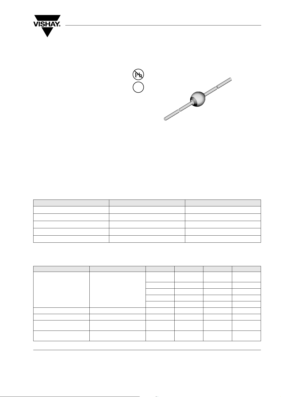
Ultra Fast Avalanche Sinterglass Diode
Features
• Glass passivated junction
• Hermetically sealed package
• Very low switching losses
• Low reverse current
• High reverse voltage
• Lead (Pb)-free component
• Component in accordance to RoHS 2002/95/EC
and WEEE 2002/96/EC
e2
BYV26
Vishay Semiconductors
949539
Applications
Switched mode power supplies
High-frequency inverter circuits
Terminals: Plated axial leads, solderable per
MIL-STD-750, Method 2026
Polarity: Color band denotes cathode end
Mounting Position: Any
Mechanical Data
Weight: approx. 369 mg
Case: SOD-57 Sintered glass case
Parts Table
Part Type differentiation Package
BYV26A V
BYV26B V
BYV26C V
BYV26D V
BYV26E V
= 200 V; I
R
= 400 V; I
R
= 600 V; I
R
= 800 V; I
R
= 1000 V; I
R
= 1 A SOD-57
FAV
= 1 A SOD-57
FAV
= 1 A SOD-57
FAV
= 1 A SOD-57
FAV
= 1 A SOD-57
FAV
Absolute Maximum Ratings
T
= 25 °C, unless otherwise specified
amb
Parameter Test condition Part Symbol Val ue Unit
Reverse voltage = Repetitive
peak reverse voltage
Peak forward surge current t
Average forward current I
Non repetitive reverse
avalanche energy
Junction and storage
temperature range
see electrical characteristics BYV26A V
BYV26B V
BYV26C V
BYV26D V
BYV26E V
= 10 ms, half sinewave I
p
I
= 1 A, inductive load E
(BR)R
R
R
R
R
R
T
= V
= V
= V
= V
= V
FSM
FAV
= T
j
R
RRM
RRM
RRM
RRM
RRM
stg
200 V
400 V
600 V
800 V
1000 V
30 A
1A
10 mJ
- 55 to + 175 °C
Document Number 86040
Rev. 1.6, 14-Apr-05
www.vishay.com
1
BYV26
Vishay Semiconductors
Maximum Thermal Resistance
T
= 25 °C, unless otherwise specified
amb
Parameter Test condition Symbol Valu e Unit
Junction ambient l = 10 mm, T
Electrical Characteristics
T
= 25 °C, unless otherwise specified
amb
Parameter Test condition Par t Symbol Min Ty p. Max Unit
Forward voltage I
Reverse current V
Reverse breakdown voltage I
Reverse recovery time I
= 1 A V
F
I
= 1 A, Tj = 175 °C V
F
= V
R
RRM
V
= V
R
= 100 µA BYV26A V
R
= 0.5 A, IR = 1 A, iR = 0.25 A BYV26A-
F
, Tj = 150 °C I
RRM
= constant R
L
BYV26B V
BYV26C V
BYV26D V
BYV26E V
BYV26C
BYV26D-
BYV26E
thJA
F
F
I
R
R
(BR)R
(BR)R
(BR)R
(BR)R
(BR)R
t
rr
t
rr
45 K/W
2.5 V
1.3 V
5 µA
100 µA
300 V
500 V
700 V
900 V
1100 V
30 ns
75 ns
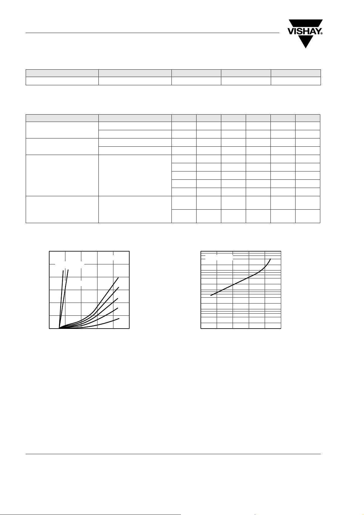
Typical Characteristics (Tamb = 25 °C unless otherwise specified)
600
VR=V
RRM
200V
400V
600V
800V
1000V
200
R
P - Maximum Reverse Power Dissipation (mW
95 9728
500
R
=45K/W
thJA
400
R
= 100 K/W
300
200
100
0
0 40 80 120 160
thJA
Tj– Junction Temperature (° C)
Figure 1. Max. Reverse Power Dissipation vs. Junction
Temperature
R
I - Reverse Current ( µA)
95 9729
1000
VR=V
RRM
100
10
1
0 40 80 120 160
Tj– Junction Temperature ( °C)
Figure 2. Max. Reverse Current vs. Junction Temperature
200
www.vishay.com
2
Document Number 86040
Rev. 1.6, 14-Apr-05

1.2
1.0
0.8
0.6
0.4
R
= 100 K/W
thJA
0.2
FAV
I - Average Forward Current ( A )
0
0 40 80 120 160
- Ambient Temperature ( °C)
T
95 9730
amb
R
thJA
=45K/W
200
Vishay Semiconductors
40
35
30
25
20
15
10
D
C - Diode Capacitance ( pF )
5
0
0.1 1 10 100
V - Reverse Voltage(V)
16380
R
BYV26C
BYV26
f=1MHz
Figure 3. Max. Average Forward Current vs. Ambient Temperature
10
Tj=175°C
1
Tj=25°C
10723566
VF- Forward Voltage(V)
F
I - Forward Current(A)
0.001
95 9731
0.1
0.01
Figure 4. Max. Forward Current vs. Forward Voltage
Package Dimensions in mm (Inches)
Sintered Glass Case
SOD-57
Cathode Identification
40
35
30
25
20
15
10
D
C - Diode Capacitance ( pF )
16381
3.6 (0.140)max.
Figure 5. Diode Capacitance vs. Reverse Voltage
f=1MHz
BYV26E
5
0
0.1 1 10 100
V - Reverse Voltage(V)
R
Figure 6. Diode Capacitance vs. Reverse Voltage
94 9538
ISO Method E
0.82 (0.032) max.
26(1.014) min.
Document Number 86040
Rev. 1.6, 14-Apr-05
4.0 (0.156) max.
26(1.014) min.
www.vishay.com
3

BYV26
Vishay Semiconductors
Ozone Depleting Substances Policy Statement
It is the policy of Vishay Semiconductor GmbH to
1. Meet all present and future national and international statutory requirements.
2. Regularly and continuously improve the performance of our products, processes, distribution and operating
systems with respect to their impact on the health and safety of our employees and the public, as well as
their impact on the environment.
It is particular concern to control or eliminate releases of those substances into the atmosphere which are
known as ozone depleting substances (ODSs).
The Montreal Protocol (1987) and its London Amendments (1990) intend to severely restrict the use of ODSs
and forbid their use within the next ten years. Various national and international initiatives are pressing for an
earlier ban on these substances.
Vishay Semiconductor GmbH has been able to use its policy of continuous improvements to eliminate the use
of ODSs listed in the following documents.
1. Annex A, B and list of transitional substances of the Montreal Protocol and the London Amendments
respectively
2. Class I and II ozone depleting substances in the Clean Air Act Amendments of 1990 by the Environmental
Protection Agency (EPA) in the USA
3. Council Decision 88/540/EEC and 91/690/EEC Annex A, B and C (transitional substances) respectively.
Vishay Semiconductor GmbH can certify that our semiconductors are not manufactured with ozone depleting
substances and do not contain such substances.
We reserve the right to make changes to improve technical design
and may do so without further notice.
Parameters can vary in different applications. All operating parameters must be validated for each
customer application by the customer. Should the buyer use Vishay Semiconductors products for any
unintended or unauthorized application, the buyer shall indemnify Vishay Semiconductors against all
claims, costs, damages, and expenses, arising out of, directly or indirectly, any claim of personal
damage, injury or death associated with such unintended or unauthorized use.
Vishay Semiconductor GmbH, P.O.B. 3535, D-74025 Heilbronn, Germany
www.vishay.com
4
Document Number 86040
Rev. 1.6, 14-Apr-05

Legal Disclaimer Notice
Vishay
Document Number: 91000 www.vishay.com
Revision: 08-Apr-05 1
Notice
Specifications of the products displayed herein are subject to change without notice. Vishay Intertechnology, Inc.,
or anyone on its behalf, assumes no responsibility or liability for any errors or inaccuracies.
Information contained herein is intended to provide a product description only. No license, express or implied, by
estoppel or otherwise, to any intellectual property rights is granted by this document. Except as provided in Vishay's
terms and conditions of sale for such products, Vishay assumes no liability whatsoever, and disclaims any express
or implied warranty, relating to sale and/or use of Vishay products including liability or warranties relating to fitness
for a particular purpose, merchantability, or infringement of any patent, copyright, or other intellectual property right.
The products shown herein are not designed for use in medical, life-saving, or life-sustaining applications.
Customers using or selling these products for use in such applications do so at their own risk and agree to fully
indemnify Vishay for any damages resulting from such improper use or sale.
 Loading...