

PD-20526 rev. B 10/98
T
1 3
2
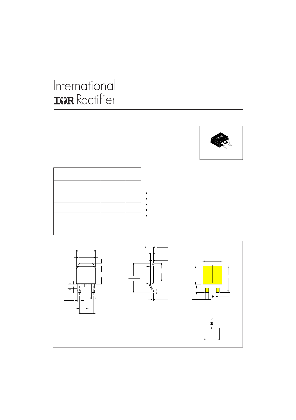
50WQ10FN
SCHOTTKY RECTIFIER 5.5 Amp
D-Pak (TO-252AA)
Major Ratings and Characteristics
Characteristics 50WQ10FN Units
I
Rectangular 5.5 A
F(AV)
waveform
V
RRM
I
@ tp = 5 µs sine 330 A
FSM
@ 5 Apk, TJ = 125°C 0.63 V
V
F
100 V
Description/Features
The 50WQ10FN surface mount Schottky rectifier has been
designed for applications requiring low forward drop and small
foot prints on PC board. Typical applications are in disk drives,
switching power supplies, converters, free-wheeling diodes,
battery charging, and reverse battery protection.
Popular D-PAK outline
Small foot print, surface moutable
Low forward voltage drop
High frequency operation
Guard ring for enhanced ruggedness and long term
reliability
TJrange - 40 to 150 °C
6.73 (0.26)
6.35 (0.25)
1.02 (0.04)
0.64 (0.03)
1.52 (0.06)
1.15 (0.04)
2x
1.14 (0.04)
0.76 (0.03)
2.28 (0.09)
2x
5.46 (0.21)
5.21 (0.20)
4
123
6.22 (0.24)
5.97 (0.23)
0.89 (0.03)
3x
0.64 (0.02)
4.57 (0.18)
1.27 (0.05)
0.88 (0.03)
10.42 (0.41)
9.40 (0.37)
Conform to JEDEC outline D-Pak (Similar to TO-252AA)
Dimensions in millimeters and (inches)
2.38 (0.09)
2.19 (0.08)
1.14 (0.04)
0.89 (0.03)
0.58 (0.02)
0.46 (0.02)
6.45 (0.24)
5.68 (0.22)
0.51 (0.02)
MIN.
0.58 (0.02)
0.46 (0.02)
MINIMUM RECOMMENDED FOOTPRIN
5.97 (0.24)
2x 2.54 (0.10)
6.48 (0.26)
1.65 (0.06)
2X
Cathode
Anode
BASE
2.28 (0.09)
Anode
10.67 (0.42)
2X
1www.irf.com
50WQ10FN
PD-20526 rev. B 10/98
Voltage Ratings
Part number 50WQ10FN
VRMax. DC Reverse Voltage (V)
V
Max. Working Peak Reverse Voltage (V)
RWM
100
Absolute Maximum Ratings
Parameters 50WQ10FN Units Conditions
I
Max. Average Forward Current 5.5 A 50% duty cycle @ TC = 135 °C, rectangular wave form
F(AV)
* See Fig. 5
I
Max. Peak One Cycle Non-Repetitive 330 5µs Sine or 3µs Rect. pulse
FSM
Surge Current * See Fig. 7 110 10ms Sine or 6ms Rect. pulse
A
Following any rated
load condition and
with rated V
RRM
Electrical Specifications
Parameters 50WQ10FN Units Conditions
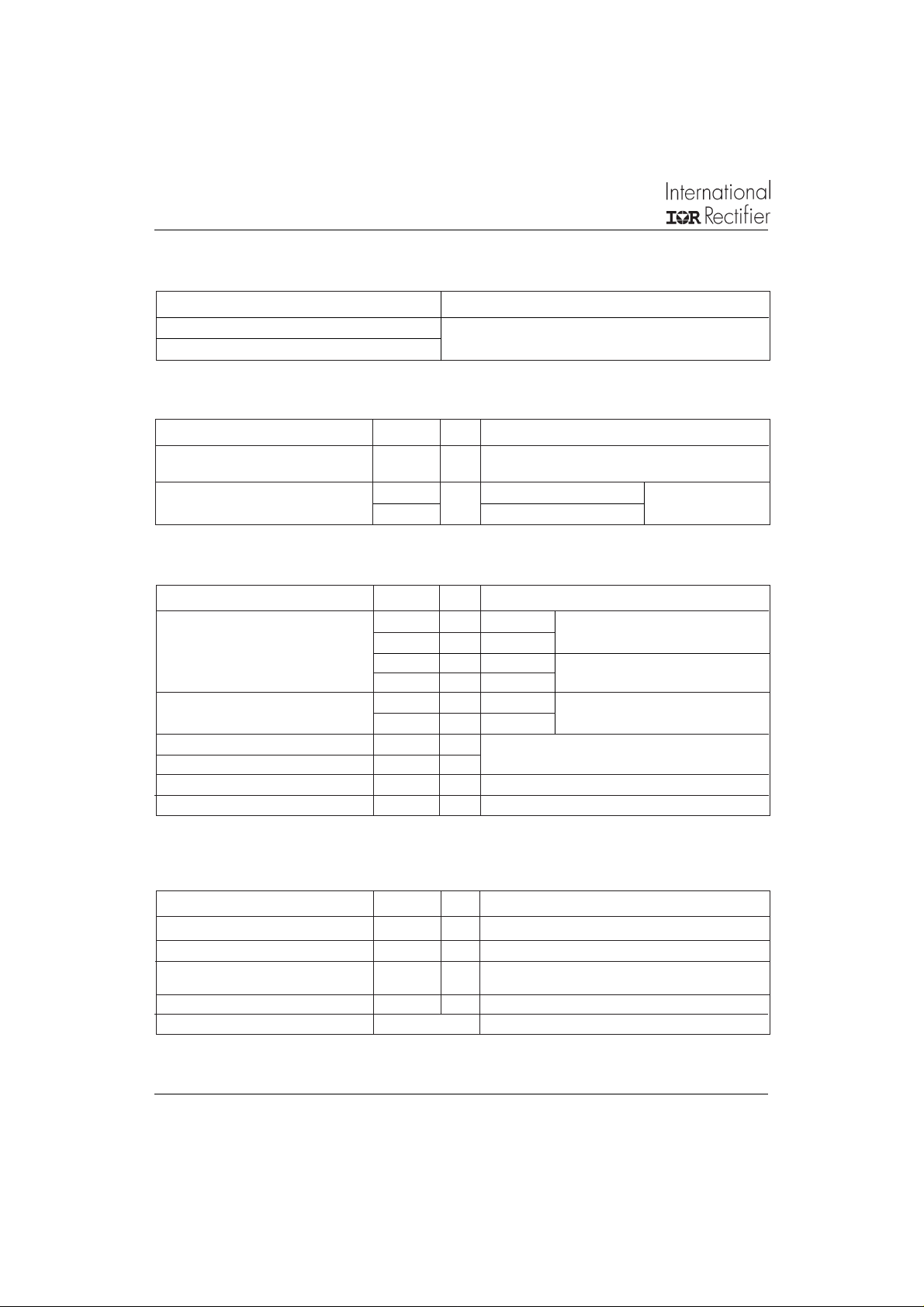
VFMMax. Forward Voltage Drop 0.77 V @ 5A
* See Fig. 1 (1 ) 0.91 V @ 10A
0.63 V @ 5A
0.74 V @ 10A
IRMMax. Reverse Leakage Current 1 mA TJ = 25 °C
* See Fig. 2 (1 ) 4 mA T
V
Threshold Voltage 0.47 V T
F(TO)
= 125 °C
J
= TJ max.
J
rtForward Slope Resistance 21.4 6 mΩ
CTTypical Junction Capacitance 183 pF VR = 5VDC, (test signal range 100Khz to 1Mhz) 25 °C
LSTypical Series Inductance 5.0 nH Measured lead to lead 5mm from package body
(1) Pulse Width < 300µs, Duty Cycle < 2%
TJ = 25 °C
T
= 125 °C
J
V
= rated V
R
R
applied
Thermal-Mechanical Specifications
Parameters 50WQ10FN Units Conditions
TJMax. Junction Temperature Range -40 to 150 °C
Max. Storage Temperature Range -40 to 150 °C
T
stg
R
Max. Thermal Resistance Junction 3.0 °C/W DC operation * See Fig. 4
thJC
to Case
wt Approximate Weight 0.3 (0.01) g (oz.)
Case Style D - PAK Similar to TO-252AA
2
www.irf.com

50WQ10FN
PD-20526 rev. B 10/98
1000
100
10
T = 150°C
J
R
1
125°C
100°C
0.1
0.01
100
F
T = 150°C
J
T = 125°C
J
T = 25°C
10
Instantaneous Forward Current - I (A)
J
Reverse Current - I (mA)
0.001
0.0001
0 102030405060708090100
Fig. 2 - Typical Values of Reverse Current
1000
T
75°C
50°C
25°C
Reverse Voltage - V (V)
R
Vs. Reverse Voltage
T = 25°C
J
100
1
00.511.522.533.5
Forward Voltage Drop - V (V)
Fig. 1 - Maximum Forward Voltage Drop Characteristics
10
D = 0.75
D = 0.50
D = 0.33
1
thJC
D = 0.25
D = 0.20
0.1
Single Pulse
Thermal Impedance Z (°C/W)
0.01
0.00001 0.0001 0.001 0.01 0.1 1
(Thermal Resistance)
t , Rectangular Pulse Duration (Seconds)
1
Fig. 4 - Maximum Thermal Impedance Z
www.irf.com
Junction Capacitance - C (pF)
10
0 20406080100
FM
Reverse Voltage - V (V)
R
Fig. 3 - Typical Junction Capacitance
Vs. Reverse Voltage
P
DM
t
1
t
DM
2
12
thJC
C
Notes:
1. Duty factor D = t / t
2. Peak T = P x Z + T
J
Characteristics
thJC
3
50WQ10FN
PD-20526 rev. B 10/98
150
145
DC
140
135
Square wave (D = 0.50)
80% Rated V applied
130
R
125
Allowa ble Cas e Temperatu re - (°C)
see note (2)
120
012345678
Average Forward Current - I (A)
Fig. 5 - Maximum Allowable Case Temperature
Vs. Average Forward Current
1000
FSM
F(AV)
At Any Rated Load Condition
And With Rated V Applied
Following Surge
RRM
5.5
5
4.5
4
D = 0.20
D = 0.25
D = 0.33
D = 0.50
D = 0.75
3.5
3
RMS Limit
2.5
2
1.5
1
Average Power Loss - (Watts)
0.5
0
012345678
Average Forward Current - I (A)
Fig. 6 - Forward Power Loss Characteristics
DC
F(AV)
(2) Formula used: TC = TJ - (Pd + Pd
Pd = Forward Power Loss = I
= Inverse Power Loss = VR1 x IR (1 - D); IR @ V
Pd
REV
F(AV)
4
Non-Repetitive Surge Current - I (A)
100
10 100 1000 10000
Square Wave Pulse Duration - t (microsec)
Fig. 7 - Maximum Non-Repetitive Surge Current
) x R
REV
x VFM @ (I
;
thJC
/ D) (see Fig. 6);
F(AV)
= 80% rated V
R1
R
p
www.irf.com
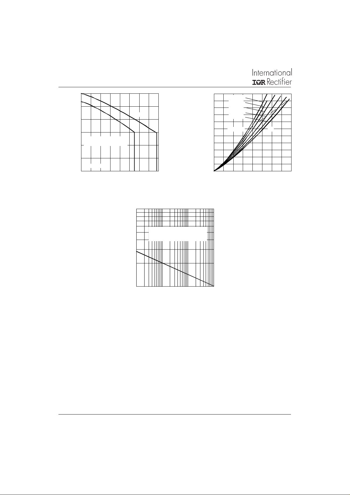
Marking Information
EXAMPLE: THIS IS AN 50WQ10FN
Tape & Reel Information
TR
FEED DIRECTION
4.1 (0.16)
3.9 (0.15)
2.1 (0.83)
1.9 (0.07)
12.1 (0.48)
11.9 (0.47)
INTERNATIONAL
RECTIFIER LOGO
ASSEMBLY
LOT CODE
1.85 (0.07)
1.65 (0.06)
1.85 (0.07)
1.65 (0.06)
DIA.
2.6 (0.10)
1.5 (0.06)
7.6 (0.30)
7.4 (0.29)
DIA.
(K)
50WQ10FN
9712
5K3A
(A) (A)
0.35 (0.01)
0.25 (0.01)
7.0 (0.28)
6.8 (0.26)
2.75 (0.11)
2.55 (0.10)
50WQ10FN
PD-20526 rev. B 10/98
PART NUMBER
DATE CODE (YYWW)
YY = YEAR
WW = WEEK
16.3 (0.64)
15.7 (0.62)
375 (14.17)
DIA. MAX.
TRR
FEED DIRECTION
TRL
FEED DIRECTION
13 (0.52) DIA.
4.1 (0.16)
3.9 (0.15)
2.1 (0.83)
1.9 (0.07)
8.1 (0.32)
7.9 (0.31)
4.1 (0.16)
3.9 (0.15)
2.1 (0.83)
1.9 (0.07)
8.1 (0.32)
7.9 (0.31)
1.85 (0.07)
1.65 (0.06)
1.85 (0.07)
1.65 (0.06)
7.6 (0.30)
7.4 (0.29)
2.6 (0.10)
1.5 (0.06)
1.85 (0.07)
1.65 (0.06)
1.85 (0.07)
1.65 (0.06)
7.6 (0.30)
7.4 (0.29)
2.6 (0.10)
1.5 (0.06)
22.4 (0.88)
50 (1.97) DIA.
DIA.
DIA.
0.35 (0.01)
0.25 (0.01)
10.6 (0.42)
10.4 (0.41)
DIA.
DIA.
2.75 (0.11)
2.55 (0.10)
0.35 (0.01)
0.25 (0.01)
10.6 (0.42)
10.4 (0.41)
2.75 (0.11)
2.55 (0.10)
TO-252AA Tape & Reel
When ordering, indicate the part
number, part orientation, and the
quantity. Quantities are in multiples
of 2,000 pieces per reel for TR and
multiples of 3,000 pieces per reel
for both TRL and TRR.
16.3 (0.64)
15.7 (0.62)
16.3 (0.64)
15.7 (0.62)
www.irf.com
5

50WQ10FN
PD-20526 rev. B 10/98
WORLD HEADQUARTERS: 233 Kansas St., El Segundo, California 90245 U.S.A. Tel: (310) 322 3331. Fax: (310) 322 3332.
EUROPEAN HEADQUARTERS: Hurst Green, Oxted, Surrey RH8 9BB, U.K. Tel: ++ 44 1883 732020. Fax: ++ 44 1883 733408.
IR SOUTHEAST ASIA: 1 Kim Seng Promenade, Great World City West Tower,13-11, Singapore 237994. Tel: ++ 65 838 4630.
http://www.irf.com Fax-On-Demand: +44 1883 733420 Data and specifications subject to change without notice.
6
IR CANADA: 15 Lincoln Court, Brampton, Markham, Ontario L6T3Z2. Tel: (905) 453 2200. Fax: (905) 475 8801.
IR GERMANY: Saalburgstrasse 157, 61350 Bad Homburg. Tel: ++ 49 6172 96590. Fax: ++ 49 6172 965933.
IR ITALY: Via Liguria 49, 10071 Borgaro, Torino. Tel: ++ 39 11 4510111. Fax: ++ 39 11 4510220.
IR FAR EAST: K&H Bldg., 2F, 30-4 Nishi-Ikebukuro 3-Chome, Toshima-Ku, Tokyo, Japan 171. Tel: 81 3 3983 0086.
IR TAIWAN: 16 Fl. Suite D.207, Sec. 2, Tun Haw South Road, Taipei, 10673, Taiwan. Tel: 886 2 2377 9936.
www.irf.com
 Loading...