Vishay High Power Products
Medium Power Thyristors
(Stud Version), 50 A
FEATURES
• High current rating
• Excellent dynamic characteristics
• dV/dt = 1000 V/µs option
• Superior surge capabilities
• Standard package
• Metric threads version available
50RIA Series
RoHS
COMPLIANT
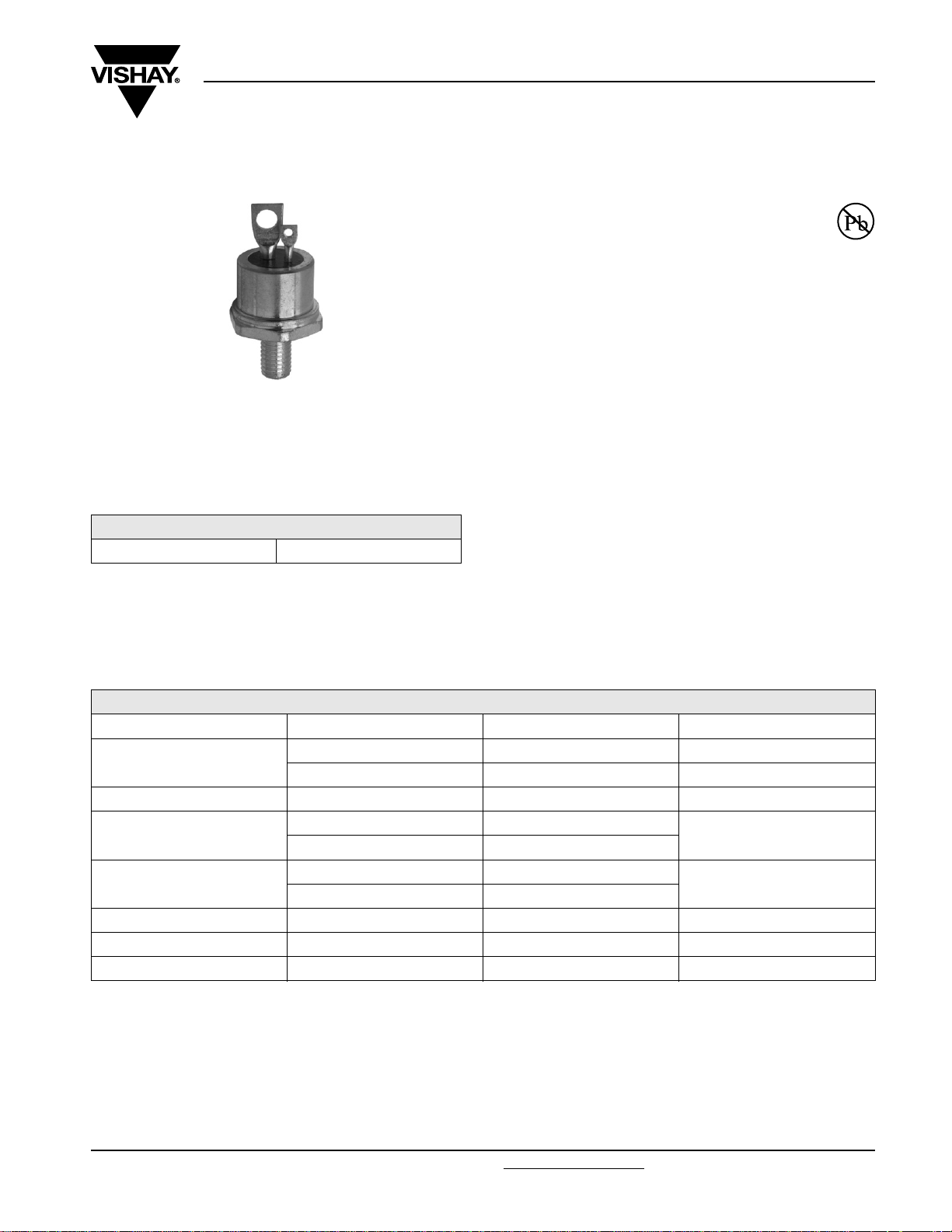
TO-208AC (TO-65)
• Types up to 1200 V V
DRM/VRRM
• RoHS compliant
TYPICAL APPLICATIONS
• Phase control applications in converters
PRODUCT SUMMARY
I
T(AV)
50 A
• Lighting circuits
• Battery charges
• Regulated power supplies and temperature and speed
control circuit
• Can be supplied to meet stringent military, aerospace and
other high reliability requirements
MAJOR RATINGS AND CHARACTERISTICS
PARAMETER TEST CONDITIONS VALUES UNITS
I
T(AV)
I
T(RMS)
I
TSM
2
I
t
V
DRM/VRRM
t
q
T
J
T
C
50 Hz 1430
60 Hz 1490
50 Hz 10.18
60 Hz 9.30
Typical 110 µs
50 A
94 °C
80 A
A
kA2s
100 to 1200 V
- 40 to 125 °C
Document Number: 93711 For technical questions, contact: ind-modules@vishay.com
Revision: 19-Sep-08 1
www.vishay.com

50RIA Series
Vishay High Power Products
Medium Power Thyristors
(Stud Version), 50 A
ELECTRICAL SPECIFICATIONS
VOLTAGE RATINGS
V
DRM/VRRM
TYPE NUMBER
VOLTAGE
CODE
REPETITIVE PEAK AND
OFF-STATE VOLTAGE
10 100 150
20 200 300
40 400 500
50RIA
60 600 700
80 800 900
100 1000 1100
120 1200 1300
Notes
(1)
Units may be broken over non-repetitively in the off-state direction without damage, if dI/dt does not exceed 20 A/µs
(2)
For voltage pulses with tp ≤ 5 ms
ABSOLUTE MAXIMUM RATINGS
PARAMETER SYMBOL TEST CONDITIONS VALUES UNITS
Maximum average on-state current
at case temperature
Maximum RMS on-state current I
Maximum peak, one-cycle
non-repetitive surge current
2
Maximum I
Maximum I
t for fusing I2t
2
√t for fusing I2√t
Low level value of threshold voltage V
High level value of threshold voltage V
Low level value of on-state
slope resistance
High level value of on-state
slope resistance
Maximum on-state voltage V
Maximum holding current I
Latching current I
I
T(AV)
T(RMS)
I
TSM
T(TO)1
T(TO)2
r
t1
r
t2
TM
H
L
, MAXIMUM
V
, MAXIMUM NON-REPETITIVE
V
RSM
(1)
PEAK VOLTAGE
V
(2)
I
DRM/IRRM
AT T
= TJ MAXIMUM
J
MAXIMUM
mA
15
180° sinusoidal conduction
50 A
94 °C
80 A
t = 10 ms
t = 8.3 ms 1490
t = 10 ms
t = 8.3 ms 1255
t = 10 ms
t = 8.3 ms 9.30
t = 10 ms
t = 8.3 ms 6.56
No voltage
reapplied
100 % V
RRM
reapplied
No voltage
reapplied
100 % V
RRM
reapplied
Sinusoidal half wave,
initial T
= TJ maximum
J
t = 0.1 to 10 ms, no voltage reapplied,
T
= TJ maximum
J
(16.7 % x π x I
(π x I
< I < 20 x π x I
T(AV)
(16.7 % x π x I
(π x I
< I < 20 x π x I
T(AV)
T(AV)
T(AV)
< I < π x I
T(AV)
< I < π x I
T(AV)
), TJ = TJ maximum 0.94
T(AV)
), TJ = TJ maximum 1.08
), TJ = TJ maximum 4.08
T(AV)
), TJ = TJ maximum 3.34
1430
1200
10.18
7.20
101.8 kA
Ipk = 157 A, TJ = 25 °C 1.60 V
TJ = 25 °C, anode supply 22 V, resistive load,
= 2 A
initial I
T
200
Anode supply 6 V, resistive load 400
A
kA2s
V
mΩ
mA
2
√s
www.vishay.com For technical questions, contact: ind-modules@vishay.com
Document Number: 93711
2 Revision: 19-Sep-08

50RIA Series
Medium Power Thyristors
Vishay High Power Products
(Stud Version), 50 A
SWITCHING
PARAMETER SYMBOL TEST CONDITIONS VALUES UNITS
T
= 125 °C, VDM = Rated V
V
≤ 600 V
Maximum rate of
rise of turned-on current
DRM
≤ 1600 V 100
V
DRM
Typical delay time t
Typical turn-off time t
dI/dt
d
q
C
Gate pulse = 20 V, 15 Ω, t
I
= (2 x rated dI/dt) A
TM
TC = 25 °C, VDM = Rated V
Gate pulse = 10 V, 15 Ω source, t
TC = 125 °C, ITM = 50 A, reapplied dV/dt = 20 V/µs
dIr/dt = - 10 A/µs, V
= 50 V
R
BLOCKING
PARAMETER SYMBOL TEST CONDITIONS VALUES UNITS
= TJ maximum linear to 100 % rated V
T
Maximum critical rate of rise of
off-state voltage
dV/dt
Note
(1)
Available with dV/dt = 1000 V/µs, to complete code add S90 i.e. 50RIA120S90
J
T
= TJ maximum linear to 67 % rated V
J
,
DRM
= 6 µs, tr = 0.1 µs maximum
p
, ITM = 10 A dc resistive circuit
DRM
= 20 µs
p
DRM
DRM
200
0.9
110
200
500
(1)
A/µs
µs
V/µs
TRIGGERING
PARAMETER SYMBOL TEST CONDITIONS VALUES UNITS
Maximum peak gate power P
Maximum average gate power P
Maximum peak positive gate current I
Maximum peak positive gate voltage +V
Maximum peak negative gate voltage -V
DC gate current required to trigger I
DC gate voltage required to trigger V
DC gate current not to trigger I
DC gate voltage not to trigger V
GM
G(AV)
GM
GT
GT
GD
GD
TJ = TJ maximum, tp ≤ 5 ms 10
GM
GM
TJ = - 40 °C
= 25 °C 100
J
= 125 °C 50
T
J
TJ = - 40 °C 3.5
T
= 25 °C 2.5
J
TJ = TJ maximum,
V
= Rated voltage
DRM
Maximum required gate trigger
current/voltage are the lowest
value which will trigger all units 6 V
anode to cathode applied
Maximum gate current/voltage not
to trigger is the maximum value
which will not trigger any unit with
TJ = TJ maximum 0.2 V
rated V
anode to cathode
DRM
applied
2.5
W
2.5 A
20
10
250
mAT
5.0 mA
V
V
Document Number: 93711 For technical questions, contact: ind-modules@vishay.com
www.vishay.com
Revision: 19-Sep-08 3

50RIA Series
Vishay High Power Products
Medium Power Thyristors
(Stud Version), 50 A
THERMAL AND MECHANICAL SPECIFICATIONS
PARAMETER SYMBOL TEST CONDITIONS VALUES UNITS
Maximum operating junction and
storage temperature range
Maximum thermal resistance,
junction to case
Maximum thermal resistance,
case to heatsink
Allowable mounting torque
Approximate weight
Case style See dimensions - link at the end of datasheet TO-208AC (TO-65)
ΔR
CONDUCTION
thJC
CONDUCTION ANGLE SINUSOIDAL CONDUCTION RECTANGULAR CONDUCTION TEST CONDITIONS UNITS
180° 0.078 0.057
120° 0.094 0.098
90° 0.120 0.130
60° 0.176 0.183
30° 0.294 0.296
Note
• The table above shows the increment of thermal resistance R
T
R
R
J
, T
thJC
thCS
Stg
DC operation 0.35
Mounting surface, smooth, flat and greased 0.25
Non-lubricated threads
Lubricated threads
- 40 to 125 °C
+ 0 - 10 %
3.4
(30)
2.3
+ 0 - 10 %
(lbf · in)
(20)
28 g
1.0 oz.
T
= TJ maximum K/W
J
when devices operate at different conduction angles than DC
thJC
K/W
N · m
130
120
110
100
Maxi mum All owable Case Tempera ture (°C)
90
0 102030405060
50RIA Series
R (DC) = 0.35 K/W
thJC
Conduction Angl e
30°
60°
90°
120°
180°
Average On-state Current (A)
130
120
110
100
90
Maximum Allowable Case Temperature (°C)
80
0 1020304050607080
50RIA Series
R (DC) = 0.35 K/W
thJC
Conduction Per iod
90°
60°
30°
Average On-state Current (A)
120°
180°
DC
Fig. 1 - Current Ratings Characteristics Fig. 2 - Current Ratings Characteristics
www.vishay.com For technical questions, contact: ind-modules@vishay.com
Document Number: 93711
4 Revision: 19-Sep-08

50RIA Series
80
70
60
50
40
30
20
10
Maximum Average On-state Power Loss (W)
0
180°
120°
90°
60°
30°
RMS Limi t
Conducti on Angle
50RIA Series
T = 125°C
J
0 1020304050
Average On-state Current (A)
Fig. 3 - On-State Power Loss Characteristics
100
Maximum Average On-state Power Loss (W)
DC
90
180°
120°
80
90°
70
60°
30°
60
50
RMS Limi t
40
30
20
10
0
0 1020304050607080
Average On-state Current (A)
Conductio n Period
50RIA Series
T = 125°C
J
Fig. 4 - On-State Power Loss Characteristics
Medium Power Thyristors
(Stud Version), 50 A
Peak Half Sine Wave On-state Current (A)
Peak Half Sine Wave On-state Current (A)
Vishay High Power Products
1300
1200
1100
1000
900
800
700
600
Number Of Equal Amplit ude Half Cycle Current Pul ses (N)
Fig. 5 - Maximum Non-Repetitive Surge Current
1500
1400
1300
1200
1100
1000
900
800
700
600
500
Fig. 6 - Maximum Non-Repetitive Surge Current
At Any Rated Load Condition And With
Rated V Applied Following Surge.
RRM
50RIA Series
110100
Maximum Non Repetitive Surge Current
Versus Pulse Train Duration. Control
Of Co ndu ct ion May Not Be Mai ntai ned.
50RIA Series
0.01 0.1 1
Pulse Train Duration (s)
Initial T = 125°C
J
@ 60 Hz 0.0083 s
@ 50 Hz 0.0100 s
Initial T = 125°C
No Vol tage Reapplied
Rated V Reapplied
J
RRM
1000
100
T = 25°C
J
T = 125°C
10
Instantaneous On-state Current (A)
1
0.5 1 1.5 2 2.5 3 3.5 4 4.5
Instantaneous On-state Voltage (V)
J
50RIA Series
Fig. 7 - Forward Voltage Drop Characteristics
Document Number: 93711 For technical questions, contact: ind-modules@vishay.com
www.vishay.com
Revision: 19-Sep-08 5

50RIA Series
A
Vishay High Power Products
1
Steady Stat e Value
R = 0.35 K/W
thJ-hs
Transient Thermal Impedance Z (K/W)
Instantaneo us Gate Voltage (V)
thJ-hs
0.1
0.01
0.001 0.01 0.1 1 10
100
Rectangular gate pulse
a) Recommended load line for
rated di/dt : 20V, 30 ohms; tr<=0.5 µs
b) Recommended load line for
<=30% rated di/dt : 20V, 65 ohms
tr<=1 µs
10
1
VGD
0.1
0.001 0.01 0.1 1 10 100 1000
IGD
Medium Power Thyristors
(Stud Version), 50 A
50RIA Ser ies
Square Wave Pul se Duration (s)
Fig. 8 - Thermal Impedance Z
(b)
Tj=125 °C
Instantaneous Gate Current (A)
(a)
Tj=-40 °C
Tj=25 °C
50RIA Series Frequency Li mit ed by PG(AV)
Fig. 9 - Gate Characteristics
Characteristics
thJC
(1) PGM = 10W, tp = 5ms
(2) PGM = 20W, tp = 2.5ms
(3) PGM = 50W, tp = 1ms
(4) PGM = 100W, tp = 500µs
(1)
(2)
(3) (4)
ORDERING INFORMATION TABLE
Device code
Dimensions http://www.vishay.com/doc?95334
www.vishay.com For technical questions, contact: ind-modules@vishay.com
6 Revision: 19-Sep-08
50 RIA 120 S90 M
1 - Current code
2 - Essential part number
3 - Voltage code x 10 = V
- Critical dV/dt:
4
None = 500 V/µs (standard value)
S90 = 1000 V/µs (special selection)
-
5
LINKS TO RELATED DOCUMENTS
None = Stud base TO-208AC (TO-65) 1/4" 28UNF-2
M = Stud base TO-208AC (TO-65) M6 x 1
51324
(see Voltage Ratings table)
RRM
Document Number: 93711

Legal Disclaimer Notice
Vishay
Disclaimer
All product specifications and data are subject to change without notice.
Vishay Intertechnology, Inc., its affiliates, agents, and employees, and all persons acting on its or their behalf
(collectively, “Vishay”), disclaim any and all liability for any errors, inaccuracies or incompleteness contained herein
or in any other disclosure relating to any product.
Vishay disclaims any and all liability arising out of the use or application of any product described herein or of any
information provided herein to the maximum extent permitted by law. The product specifications do not expand or
otherwise modify Vishay’s terms and conditions of purchase, including but not limited to the warranty expressed
therein, which apply to these products.
No license, express or implied, by estoppel or otherwise, to any intellectual property rights is granted by this
document or by any conduct of Vishay.
The products shown herein are not designed for use in medical, life-saving, or life-sustaining applications unless
otherwise expressly indicated. Customers using or selling Vishay products not expressly indicated for use in such
applications do so entirely at their own risk and agree to fully indemnify Vishay for any damages arising or resulting
from such use or sale. Please contact authorized Vishay personnel to obtain written terms and conditions regarding
products designed for such applications.
Product names and markings noted herein may be trademarks of their respective owners.
Document Number: 91000 www.vishay.com
Revision: 18-Jul-08 1

DIMENSIONS in millimeters (inches)
Outline Dimensions
Vishay High Power Products
TO-208AC (TO-65)
5.1/7.6
(0.2/0.3)
31 MAX.
(1.22 MAX.)
3 MIN.
(0.118 MIN.)
Ø 15 (Ø 0.59)
10.7/11.5
(0.42/0.46)
Ø 4.1 (Ø 0.16)
(0.1/0.14)
1/4"-28UNF-2A
for metric device M6 x 1
Ø 19.2 (Ø 0.75)
2.5/3.6
Ø 1.5 (Ø 0.06)
14.5 MAX.
(0.57 MAX.)
22.4 MAX.
(0.88 MAX.)
17.2/17.35
(0.67/0.68)
Across flats
1.7/1.8
(0.06/0.07)
2.7 (0.106)
Document Number: 95334 For technical questions concerning discrete products, contact: diodes-tech@vishay.com
Revision: 08-Jul-08 For technical questions concerning module products, contact: ind-modules@vishay.com
www.vishay.com
1
 Loading...