

40TPS...APbF/40TPS...PbF High Voltage Series
Vishay High Power Products
Phase Control SCR, 35 A
DESCRIPTION/FEATURES
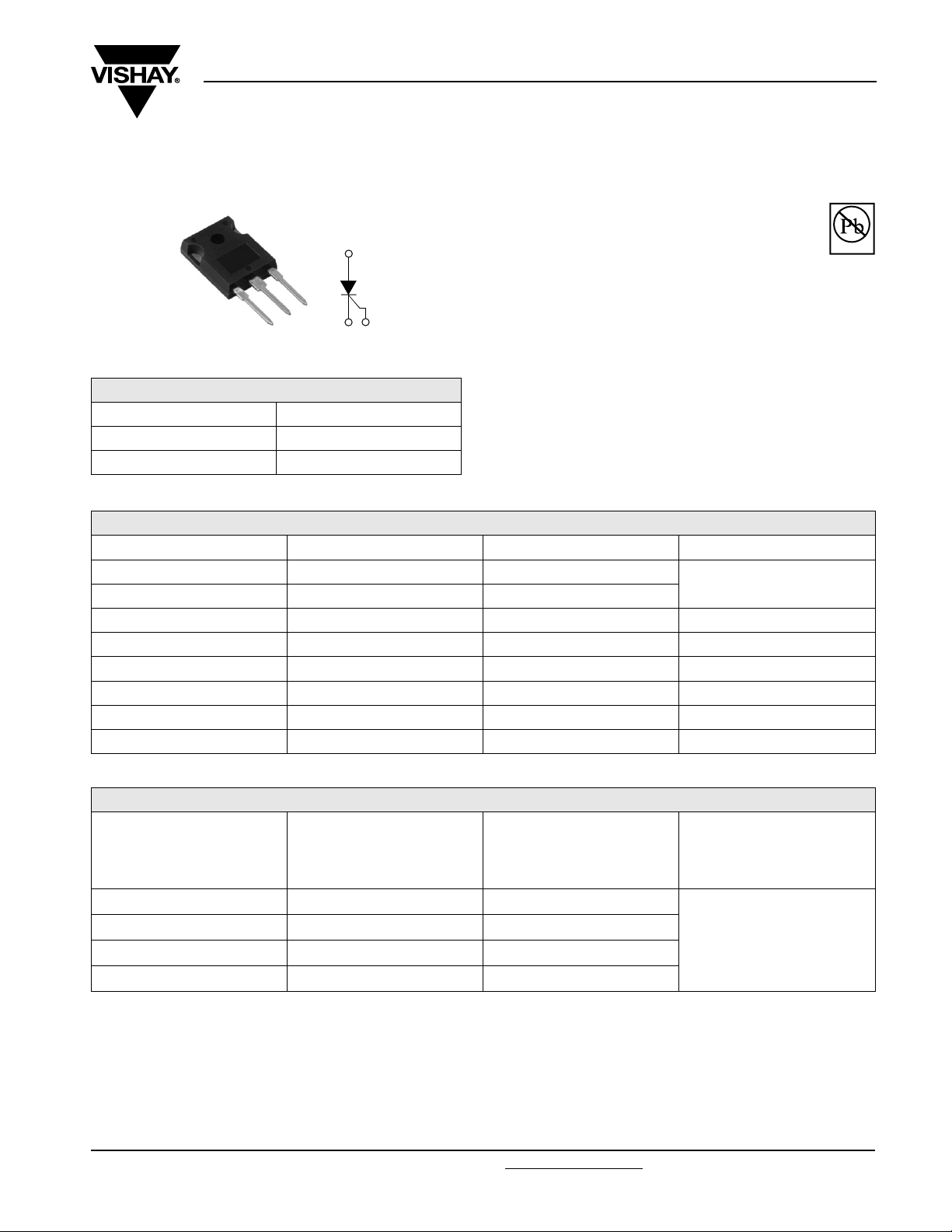
TO-2 47AC
PRODUCT SUMMARY
VT at 40 A < 1.45 V
I
TSM
V
RRM
2
(A)
1 (K)
(G) 3
500 A
800/1200 V
The 40TPS...APbF High Voltage Series of silicon
controlled rectifiers are specifically designed for
medium power switching and phase control
applications. The glass passivation technology
used has reliable operation up to 125 °C junction
temperature. Low Igt parts available.
Typical applications are in input rectification (soft start) and
these products are designed to be used with Vishay HPP
input diodes, switches and output rectifiers which are
available in identical package outlines.
This product has been designed and qualified for industrial
level and lead (Pb)-free (“PbF” suffix).
MAJOR RATINGS AND CHARACTERISTICS
PARAMETER TEST CONDITIONS VALUES UNITS
I
T(AV)
I
RMS
V
RRM/VDRM
I
TSM
V
T
dV/dt 1000 V/µs
dI/dt 100 A/µs
T
J
Sinusoidal waveform 35
55
800/1200 V
500 A
40 A, TJ = 25 °C 1.45 V
- 40 to 125 °C
A
Pb-free
Available
RoHS*
COMPLIANT
VOLTAGE RATINGS
V
RRM/VDRM
PART NUMBER
40TPS08APbF 800 900
40TPS12APbF 1200 1300
40TPS08PbF 800 900
40TPS12PbF 1200 1300
* Pb containing terminations are not RoHS compliant, exemptions may apply
Document Number: 94388 For technical questions, contact: diodes-tech@vishay.com
Revision: 12-Sep-08 1
REPETITIVE PEAK AND
OFF-STATE VOLTAGE
, MAXIMUM
V
V
, MAXIMUM
RSM
NON-REPETITIVE PEAK
REVERSE VOLTAGE
V
I
RRM/IDRM
AT 125 °C
mA
10
www.vishay.com
40TPS...APbF/40TPS...PbF High Voltage Series
Vishay High Power Products
Phase Control SCR, 35 A
ABSOLUTE MAXIMUM RATINGS
PARAMETER SYMBOL TEST CONDITIONS VALUES UNITS
Maximum average on-state current I
Maximum continuous RMS
on-state current as AC switch
Maximum peak, one-cycle
non-repetitive surge current
Maximum I
Maximum I
2
t for fusing I2t
2
√t for fusing I2√t t = 0.1 to 10 ms, no voltage reapplied 12 500 A2√s
Low level value of threshold voltage V
High level value of threshold voltage V
Low level value of on-state slope resistance r
High level value of on-state slope resistance r
Maximum peak on-state voltage V
T(AV)
I
T(RMS)
I
TSM
T(TO)1
T(TO)2
t1
t2
TM
Maximum rate of rise of turned-on current dI/dt T
Maximum holding current I
H
Maximum latching current I
Maximum reverse and direct leakage current I
Maximum rate of rise of off-state voltage 40TPS08
Maximum rate of rise of off-state voltage 40TPS12 1000
RRM/IDRM
dV/dt T
TC = 79 °C, 180° conduction half sine wave 35
10 ms sine pulse, rated V
RRM
applied
10 ms sine pulse, no voltage reapplied 600
Initial T
=
10 ms sine pulse, rated V
applied 1250
RRM
10 ms sine pulse, no voltage reapplied 1760
T
maximum
J
J
TJ = 125 °C
110 A, TJ = 25 °C 1.85 V
= 25 °C 100 A/µs
J
L
TJ = 25 °C
T
= 125 °C 10
J
= TJ maximum, linear to 80 % V
J
V
= Rated V
R
RRM/VDRM
, Rg-k = Open
DRM
55
500
1.02
1.23
9.74
7.50
150
300
0.5
500
A
2
A
V
mΩ
mA
V/µs
s
TRIGGERING
PARAMETER SYMBOL TEST CONDITIONS VALUES UNITS
Maximum peak gate power P
Maximum average gate power P
Maximum peak gate current I
Maximum peak negative gate voltage - V
Maximum required DC gate
voltage to trigger
Maximum required DC gate current to trigger I
Maximum DC gate voltage not to trigger V
Maximum DC gate current not to trigger I
GM
G(AV)
GM
V
GT
GT
GD
GD
GM
TJ = - 40 °C
= 25 °C 2.5
J
T
= 125 °C 1.7
J
Anode supply = 6 V
resistive load
TJ = - 40 °C 270
= 25 °C 150
T
J
= 125 °C 80
T
J
T
= 25 °C, for 40TPS08APbF and 40TPS12APbF 40
J
TJ = 125 °C, V
= Rated value 0.25 V
DRM
10
2.5
W
2.5 A
10 V
4.0
VT
mA
6mA
www.vishay.com For technical questions, contact: diodes-tech@vishay.com
Document Number: 94388
2 Revision: 12-Sep-08
40TPS...APbF/40TPS...PbF High Voltage Series
Phase Control SCR, 35 A
Vishay High Power Products
THERMAL AND MECHANICAL SPECIFICATIONS
PARAMETER SYMBOL TEST CONDITIONS VALUES UNITS
Maximum junction and storage
temperature range
Maximum thermal resistance,
junction to case
Maximum thermal resistance,
junction to ambient
Maximum thermal resistance,
case to heatsink
Approximate weight
Mounting torque
Marking device Case style TO-247AC
minimum 6 (5)
maximum 12 (10)
T
R
R
R
J
, T
thJC
thJA
thCS
Stg
DC operation
Mounting surface, smooth and greased 0.2
- 40 to 125 °C
0.6
40
6g
0.21 oz.
40TPS08A
40TPS12A
40TPS08
40TPS12
°C/W
kgf · cm
(lbf · in)
Document Number: 94388 For technical questions, contact: diodes-tech@vishay.com
Revision: 12-Sep-08 3
www.vishay.com

40TPS...APbF/40TPS...PbF High Voltage Series
Vishay High Power Products
130
120
110
100
90
80
70
Maximum Allowable Case Temperature (°C)
010203040
Fig. 1 - Current Rating Characteristics
130
120
110
100
90
80
70
Maximum Allowable Case Temperature (°C)
0 102030405060
Fig. 2 - Current Rating Characteristics
40TPS.. Series
R (DC) = 0.6 °C/W
thJC
Conduction A ngle
30°
60°
90°
120°
Average On-state Current (A)
40TPS.. Series
R (DC) = 0.6 °C/ W
thJC
Conduction Period
30°
60°
90°
120°
180°
DC
Average On-state Current (A)
Phase Control SCR, 35 A
180°
80
70
60
50
40
30
20
10
Maximum Average On-state Power Loss (W)
DC
180°
120°
90°
60°
30°
RM S Li m it
Conduction Period
40 TPS. . Se r ie s
T = 125°C
J
0
0 102030405060
Ave ra ge On-sta te Current (A)
Fig. 4 - On-State Power Loss Characteristics
550
At Any Rated Load Condition And With
Rated V Applied Following Surge.
500
450
400
350
ine Wa ve On-st at e Current (A)
300
4 0 TPS. . Se r i e s
Pe a k Half S
250
110100
Numbe r Of Eq ual Amplitude Half Cycle Current Pulses (N)
RRM
Init ia l T = 125°C
J
@ 6 0 Hz 0. 0 083 s
@ 5 0 Hz 0. 0 100 s
Fig. 5 - Maximum Non-Repetitive Surge Current
60
180°
120°
50
90°
60°
30°
40
30
20
10
0
Maximum Average On-state Power Loss (W)
0 5 10 15 20 25 30 35 40
Average On-state Current (A)
Conduction Angle
40TPS.. Series
T = 1 2 5 ° C
J
Fig. 3 - On-State Power Loss Characteristics
RM S Li m it
600
550
500
450
400
350
300
Peak Half Sine Wave On-state Current (A)
250
Maximum Non Repetitive Surge Current
Versus Pulse Train Dura tion. Control
Of Co nduc tion May Not Be Mainta ined.
40TPS.. Series
0.01 0.1 1
Pulse Tra in D u ra t io n ( s)
Ini t ia l T = 125°C
No Voltage Reapplied
Ra t e d V Re a p p li e d
RRM
Fig. 6 - Maximum Non-Repetitive Surge Current
J
www.vishay.com For technical questions, contact: diodes-tech@vishay.com
Document Number: 94388
4 Revision: 12-Sep-08

40TPS...APbF/40TPS...PbF High Voltage Series
100
Rectangular gate pulse
a)Recommended load line for
rated di/dt: 20 V, 30 ohms
tr = 0.5 µs, tp >= 6 µs
b)Recommended load line for
<= 30% rated di/dt: 10 V, 65 ohms
10
tr = 1 µs, tp >= 6 µs
Phase Control SCR, 35 A
100
10
Insta nt a neo us On-state Cu rrent (A )
1
0.5 1 1.5 2
Instantaneous On-state Voltage (V)
Fig. 7 - On-State Voltage Drop Characteristics
(a)
(b)
T = 2 5 ° C
J
T = 125°C
J
4 0 TPS. . Se r i e s
Vishay High Power Products
(1) PGM = 100 W, tp = 500µs
(2) PGM = 50 W, tp = 1 ms
(3) PGM = 20 W, tp = 25 ms
(4) PGM = 10 W, tp = 5 ms
TJ = -40
1
Instantaneous Gate Voltage (V)
VGD
IGD
0.1
TJ = 25
TJ = 125
°C
°
C
°C
40TPS..A Series
(2)
(3)
(4)
Frequency Limited by PG(AV)
(1)
0.001 0.01 0.1 1 10 100 1000
Instantaneous Gate Current (A)
Fig. 8 - Gate Characteristics
1
thJC
Transient Thermal Impedance Z (°C/W)
0.01
D = 0.50
D = 0.33
D = 0.25
D = 0.17
0.1
D = 0.08
Si n g l e Pu ls e
0.0001 0.001 0.01 0.1 1
Sq u a r e W a v e Pu l se D u r a t i o n ( s)
Fig. 9 - Thermal Impedance Z
Characteristics
thJC
St e a d y St a t e V a l u e
(DC Operation)
40TPS.. Ser ie s
Document Number: 94388 For technical questions, contact: diodes-tech@vishay.com
www.vishay.com
Revision: 12-Sep-08 5

40TPS...APbF/40TPS...PbF High Voltage Series
Vishay High Power Products
ORDERING INFORMATION TABLE
Device code
40 T P S 12 A PbF
1
- Current rating (40 = 40 A)
2
- Circuit configuration:
3
- Package:
4
- Type of silicon:
5
- Voltage ratings
6
-
7
-
Phase Control SCR, 35 A
51324
67
T = Thyristor
P = TO-247
S = Standard recovery rectifier
A = Low Igt selection 40 mA maximum
None = Standard Igt selection
None = Standard production
PbF = Lead (Pb)-free
08 = 800 V
12 = 1200 V
LINKS TO RELATED DOCUMENTS
Dimensions http://www.vishay.com/doc?95223
Part marking information http://www.vishay.com/doc?95226
www.vishay.com For technical questions, contact: diodes-tech@vishay.com
6 Revision: 12-Sep-08
Document Number: 94388

Legal Disclaimer Notice
Vishay
Disclaimer
All product specifications and data are subject to change without notice.
Vishay Intertechnology, Inc., its affiliates, agents, and employees, and all persons acting on its or their behalf
(collectively, “Vishay”), disclaim any and all liability for any errors, inaccuracies or incompleteness contained herein
or in any other disclosure relating to any product.
Vishay disclaims any and all liability arising out of the use or application of any product described herein or of any
information provided herein to the maximum extent permitted by law. The product specifications do not expand or
otherwise modify Vishay’s terms and conditions of purchase, including but not limited to the warranty expressed
therein, which apply to these products.
No license, express or implied, by estoppel or otherwise, to any intellectual property rights is granted by this
document or by any conduct of Vishay.
The products shown herein are not designed for use in medical, life-saving, or life-sustaining applications unless
otherwise expressly indicated. Customers using or selling Vishay products not expressly indicated for use in such
applications do so entirely at their own risk and agree to fully indemnify Vishay for any damages arising or resulting
from such use or sale. Please contact authorized Vishay personnel to obtain written terms and conditions regarding
products designed for such applications.
Product names and markings noted herein may be trademarks of their respective owners.
Document Number: 91000 www.vishay.com
Revision: 18-Jul-08 1

DIMENSIONS in millimeters and inches
Outline Dimensions
Vishay High Power Products
TO-247
(2) R/2
2 x R
(5) L1
0.10 AC
Planting
B
D
(2)
C
2 x b2
3 x b
MM
(c)
Section C - C, D - D, E - E
E
1
2
b4
(b1, b3, b5)
(b, b2, b4)
(3)
E/2
(4)
3
2 x e
S
D
L
Base metal
c1
See view B
A
A2
A
D
A
C
A1
DDE E
View B
A
(6)
Ø P
MM
Ø K BD
D2
Thermal pad
Lead assignments
HEXFET
1. - Gate
2. - Drain
3. - Source
4. - Drain
C
C
IGBTs, CoPAK
1. - Gate
2. - Collector
3. - Emitter
4. - Collector
4
(4)
E1
MM
0.01 BD
View A - A
(Datum B)
FP1
D1 (4)
Diodes
1. - Anode/open
2. - Cathode
3. - Anode
SYMBOL
MILLIMETERS INCHES
MIN. MAX. MIN. MAX. MIN. MAX. MIN. MAX.
NOTES SYMBOL
MILLIMETERS INCHES
NOTES
A 4.65 5.31 0.183 0.209 D2 0.51 1.30 0.020 0.051
A1 2.21 2.59 0.087 0.102 E 15.29 15.87 0.602 0.625 3
A2 1.50 2.49 0.059 0.098 E1 13.72 - 0.540 -
b 0.99 1.40 0.039 0.055 e 5.46 BSC 0.215 BSC
b1 0.99 1.35 0.039 0.053 FK 2.54 0.010
b2 1.65 2.39 0.065 0.094 L 14.20 16.10 0.559 0.634
b3 1.65 2.37 0.065 0.094 L1 3.71 4.29 0.146 0.169
b4 2.59 3.43 0.102 0.135 N 7.62 BSC 3
b5 2.59 3.38 0.102 0.133 FP 3.56 3.66 0.14 0.144
c 0.38 0.86 0.015 0.034 FP1 - 6.98 - 0.275
c1 0.38 0.76 0.015 0.030 Q 5.31 5.69 0.209 0.224
D 19.71 20.70 0.776 0.815 3 R 0.452 5.49 0.178 0.216
D1 13.08 - 0.515 - 4 S 5.51 BSC 0.217 BSC
Notes
(1)
Dimensioning and tolerancing per ASME Y14.5M-1994
(2)
Contour of slot optional
(3)
Dimension D and E do not include mold flash. Mold flash shall not exceed 0.127 mm (0.005") per side. These dimensions are measured at
the outermost extremes of the plastic body
(4)
Thermal pad contour optional with dimensions D1 and E1
(5)
Lead finish uncontrolled in L1
(6)
Ø P to have a maximum draft angle of 1.5 to the top of the part with a maximum hole diameter of 3.91 mm (0.154")
(7)
Outline conforms to JEDEC outline TO-247 with exception of dimension c
Document Number: 95223 For technical questions concerning discrete products, contact: diodes-tech@vishay.com
www.vishay.com
Revision: 11-Mar-08 For technical questions concerning module products, contact: ind-modules@vishay.com
1

Assembly
lot code
xxxxxxx
V P119X
A
Part Marking Information
Vishay High Power Products
TO-247
Example: This is a xxxxxxx with
Part number
C
Product version (optional):
P = Lead (Pb)-free
None = Standard
Date code:
Year 1 = 2001
Week 19
Line X
assembly lot code AC,
assembled on WW 19, 2001
in the assembly line ”X”
Document Number: 95226 For technical questions concerning discrete products, contact: diodes-tech@vishay.com
Revision: 28-Nov-08 For technical questions concerning module products, contact: ind-modules@vishay.com
www.vishay.com
1
 Loading...