

N-Channel 60-V (D-S) MOSFET
V
PRODUCT SUMMARY
V
(V)
DS
60 3 @ VGS = 10 V 240
r
DS(on)
(W)
FEATURES BENEFITS APPLICATIONS
D Low On-Resistance: 3 W
D Low Threshold: 2 V (typ)
D Low Input Capacitance: 25 pF
D Fast Switching Speed: 7.5 ns
D Low Input and Output Leakage
D Low Offset Voltage
D Low-Voltage Operation
D Easily Driven Without Buffer
D High-Speed Circuits
D Low Error Voltage
I
D
(mA)
D Direct Logic-Level Interface: TTL/CMOS
D Drivers: Relays, Solenoids, Lamps, Hammers,
Display, Memories, Transistors, etc.
D Battery Operated Systems
D Solid-State Relays
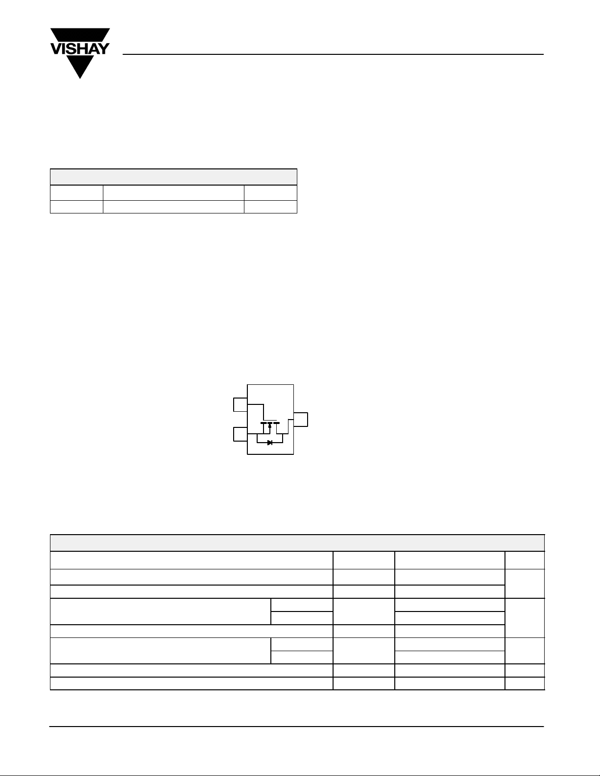
2N7002E
Vishay Siliconix
TO-236
(SOT-23)
Marking Code: 7Ewl
G
1
3
D
2
S
Top View
Ordering Information: 2N7002E-T1
E = Part Number Code for 2N7002E
w = Week Code
l = Lot Traceability
ABSOLUTE MAXIMUM RATINGS (TA = 25_C UNLESS OTHERWISE NOTED)
Parameter Symbol Limit Unit
Drain-Source Voltage V
Gate-Source Voltage V
Continuous Drain Current (TJ = 150_C)
Pulsed Drain Current
Power Dissipation
Thermal Resistance, Junction-to-Ambient R
Operating Junction and Storage Temperature Range TJ, T
a
_
TA = 25_C
TA = 70_C
TA = 25_C
TA = 70_C
I
I
DM
P
thJA
DS
GS
D
D
stg
60
"20
240
190
1300
0.35
0.22
357
-55 to 150
mA
W
_C/W
_C
Notes
a. Pulse width limited by maximum junction temperature.
Document Number: 70860
S-31987—Rev. D, 13-Oct-03
www.vishay.com
1
2N7002E
b
b
ID ^ 250 mA
Vishay Siliconix
SPECIFICATIONS (TJ = 25_C UNLESS OTHERWISE NOTED)
Parameter Symbol Test Conditions Min Typ
Static
Limits
a
Max Unit
Drain-Source Breakdown Voltage V
Gate-Threshold Voltage V
Gate-Body Leakage I
Zero Gate Voltage Drain Current I
On-State Drain Current
Drain-Source On-Resistance
Forward Transconductance
Diode Forward Voltage V
Dynamic
Total Gate Charge Q
Gate-Source Charge Q
Gate-Drain Charge Q
Input Capacitance C
Output Capacitance C
Reverse Transfer Capacitance C
Switching
Turn-On Time t
Turn-Off Time t
Notes
a. For DESIGN AID ONLY, not subject to production testing.
b. Pulse test: PW v300 ms duty cycle v2%.
c. Switching time is essentially independent of operating temperature.
a
a, c
b
(BR)DSS
GS(th)
GSS
DSS
I
D(on)
r
DS(on)
g
fs
SD
g
gs
gd
iss
oss
rss
on
off
VGS = 0 V, ID = 10 mA
VDS = VGS, ID = 250 mA
VDS = 0 V, VGS = "15 V "10 nA
VDS = 60 V, VGS = 0 V 1
VDS = 60 V, VGS = 0 V, TC = 125_C
VGS = 10 V, VDS = 7.5 V 800 1300
VGS = 4.5 V, VDS = 10 V 500 700
VGS = 10 V, ID = 250 mA 1.2 3
VGS = 4.5 V, ID = 200 mA 1.8 4
VDS = 15 V, ID = 200 mA 600 mS
IS = 200 mA, VGS = 0 V 0.85 1.2 V
VDS = 10 V, VGS = 4.5 V
^ 250 mA
I
D
VDS = 5 V, VGS = 0 V, f = 1 MHz
VDD = 10 V, RL = 40 W
ID ^ 250 mA, V
R
G
GEN
= 10 W
= 10V
60 68
1 2 2.5
500
0.4 0.6
0.06
0.06
21
7
2.5
13 20
18 25
V
mA
mA
W
nC
pF
ns
www.vishay.com
2
Document Number: 70860
S-31987—Rev. D, 13-Oct-03

TYPICAL CHARACTERISTICS (TA = 25_C UNLESS OTHERWISE NOTED)
2N7002E
Vishay Siliconix
1.0
VGS = 10, 9, 8, 7, 6 V
0.8
0.6
0.4
- Drain Current (A)
D
I
0.2
0.0
012345
VDS - Drain-to-Source Voltage (V)
5 V
4 V
3 V
On-Resistance vs. Gate-Source Voltage On-Resistance vs. Drain Current
4
3
ID @ 250 mA
2
Output Characteristics Transfer Characteristics
- On-Resistance ( Ω )
DS(on)
r
1
ID @ 75 mA
1.2
TJ = -55_C
0.9
0.6
- Drain Current (A)
D
I
0.3
0.0
01234567
- Gate-to-Source Voltage (V)
V
GS
3.5
3.0
2.5
VGS = 4.5 V
2.0
VGS = 10 V
- On-Resistance ( Ω )
DS(on)
r
1.5
1.0
0.5
25_C
125_C
0
0246810
On-Resistance vs. Junction Temperature
2.0
1.6
1.2
(Normalized)
0.8
- On-Resistance ( Ω )
DS(on)
r
0.4
0.0
-50 -25 0 25 50 75 100 125 150
Document Number: 70860
S-31987—Rev. D, 13-Oct-03
VGS = 10 V @ 250 mA
VGS = 4.5 V
@ 200 mA
TJ - Junction Temperature (_C)
0.0
0.0 0.2 0.4 0.6 0.8 1.0
I
- Drain Current (A)VGS - Gate-to-Source Voltage (V)
D
Threshold Voltage Variance Over Temperature
0.4
0.2
ID = 250 mA
-0.0
-0.2
- Variance (V)
-0.4
GS(th)
V
-0.6
-0.8
-50 -25 0 25 50 75 100 125 150
- Junction Temperature (_C)
T
J
www.vishay.com
3

2N7002E
Vishay Siliconix
TYPICAL CHARACTERISTICS (TA = 25_C UNLESS OTHERWISE NOTED)
40
32
24
16
C - Capacitance (pF)
8
0
0 5 10 15 20 25
VDS - Drain-to-Source Voltage (V)
Capacitance
C
iss
C
1.0
VDS = 30 V
= 0.25 A
I
D
0.8
0.6
0.4
oss
C
rss
- Gate-to-Source Voltage (V)
0.2
GS
V
0.0
0.0 0.1 0.2 0.3 0.4 0.5
Gate Charge
Qg - Total Gate Charge (nC)
Source-Drain Diode Forward Voltage
2
1
TJ = 85_C
- Source Current (A)
S
I
0.1
0 0.2 0.4 0.6 0.8 1.0 1.2
25_C
VSD - Source-to-Drain Voltage (V)
-55_C
www.vishay.com
4
Document Number: 70860
S-31987—Rev. D, 13-Oct-03

Legal Disclaimer Notice
Vishay
Notice
Specifications of the products displayed herein are subject to change without notice. Vishay Intertechnology, Inc.,
or anyone on its behalf, assumes no responsibility or liability for any errors or inaccuracies.
Information contained herein is intended to provide a product description only. No license, express or implied, by
estoppel or otherwise, to any intellectual property rights is granted by this document. Except as provided in Vishay's
terms and conditions of sale for such products, Vishay assumes no liability whatsoever, and disclaims any express
or implied warranty, relating to sale and/or use of Vishay products including liability or warranties relating to fitness
for a particular purpose, merchantability, or infringement of any patent, copyright, or other intellectual property right.
The products shown herein are not designed for use in medical, life-saving, or life-sustaining applications.
Customers using or selling these products for use in such applications do so at their own risk and agree to fully
indemnify Vishay for any damages resulting from such improper use or sale.
Document Number: 91000 www.vishay.com
Revision: 08-Apr-05 1

 Loading...